US7217396B2 - Microfabricated micro fluid channels - Google Patents
Microfabricated micro fluid channels Download PDFInfo
- Publication number
- US7217396B2 US7217396B2 US10/429,333 US42933303A US7217396B2 US 7217396 B2 US7217396 B2 US 7217396B2 US 42933303 A US42933303 A US 42933303A US 7217396 B2 US7217396 B2 US 7217396B2
- Authority
- US
- United States
- Prior art keywords
- channel
- micro
- substrate
- fluid
- well
- Prior art date
- Legal status (The legal status is an assumption and is not a legal conclusion. Google has not performed a legal analysis and makes no representation as to the accuracy of the status listed.)
- Expired - Lifetime, expires
Links
- 239000012530 fluid Substances 0.000 title claims abstract description 77
- 239000000758 substrate Substances 0.000 claims abstract description 131
- 238000004891 communication Methods 0.000 claims abstract description 9
- 239000000523 sample Substances 0.000 claims description 17
- 230000005661 hydrophobic surface Effects 0.000 claims description 6
- 238000001020 plasma etching Methods 0.000 claims description 4
- 238000004621 scanning probe microscopy Methods 0.000 claims description 3
- 239000000463 material Substances 0.000 description 22
- 238000005530 etching Methods 0.000 description 14
- 238000000034 method Methods 0.000 description 12
- 239000004065 semiconductor Substances 0.000 description 10
- XUIMIQQOPSSXEZ-UHFFFAOYSA-N Silicon Chemical compound [Si] XUIMIQQOPSSXEZ-UHFFFAOYSA-N 0.000 description 7
- 229910052710 silicon Inorganic materials 0.000 description 7
- 239000010703 silicon Substances 0.000 description 7
- 238000012545 processing Methods 0.000 description 6
- 239000000126 substance Substances 0.000 description 6
- 239000000976 ink Substances 0.000 description 5
- VYPSYNLAJGMNEJ-UHFFFAOYSA-N Silicium dioxide Chemical compound O=[Si]=O VYPSYNLAJGMNEJ-UHFFFAOYSA-N 0.000 description 4
- 238000003491 array Methods 0.000 description 4
- 238000005553 drilling Methods 0.000 description 4
- QJAOYSPHSNGHNC-UHFFFAOYSA-N octadecane-1-thiol Chemical compound CCCCCCCCCCCCCCCCCCS QJAOYSPHSNGHNC-UHFFFAOYSA-N 0.000 description 4
- KWYUFKZDYYNOTN-UHFFFAOYSA-M Potassium hydroxide Chemical compound [OH-].[K+] KWYUFKZDYYNOTN-UHFFFAOYSA-M 0.000 description 3
- 238000000059 patterning Methods 0.000 description 3
- 229920000642 polymer Polymers 0.000 description 3
- 238000011160 research Methods 0.000 description 3
- CSCPPACGZOOCGX-UHFFFAOYSA-N Acetone Chemical compound CC(C)=O CSCPPACGZOOCGX-UHFFFAOYSA-N 0.000 description 2
- 229910052581 Si3N4 Inorganic materials 0.000 description 2
- NRTOMJZYCJJWKI-UHFFFAOYSA-N Titanium nitride Chemical compound [Ti]#N NRTOMJZYCJJWKI-UHFFFAOYSA-N 0.000 description 2
- 238000004026 adhesive bonding Methods 0.000 description 2
- YCIMNLLNPGFGHC-UHFFFAOYSA-N catechol Chemical compound OC1=CC=CC=C1O YCIMNLLNPGFGHC-UHFFFAOYSA-N 0.000 description 2
- 239000011248 coating agent Substances 0.000 description 2
- 238000000576 coating method Methods 0.000 description 2
- PCHJSUWPFVWCPO-UHFFFAOYSA-N gold Chemical compound [Au] PCHJSUWPFVWCPO-UHFFFAOYSA-N 0.000 description 2
- 229910052737 gold Inorganic materials 0.000 description 2
- 239000010931 gold Substances 0.000 description 2
- 230000002209 hydrophobic effect Effects 0.000 description 2
- 238000004519 manufacturing process Methods 0.000 description 2
- 229910052751 metal Inorganic materials 0.000 description 2
- 239000002184 metal Substances 0.000 description 2
- 150000002739 metals Chemical class 0.000 description 2
- 150000004767 nitrides Chemical class 0.000 description 2
- 229920002120 photoresistant polymer Polymers 0.000 description 2
- 238000005498 polishing Methods 0.000 description 2
- HQVNEWCFYHHQES-UHFFFAOYSA-N silicon nitride Chemical compound N12[Si]34N5[Si]62N3[Si]51N64 HQVNEWCFYHHQES-UHFFFAOYSA-N 0.000 description 2
- 229910052814 silicon oxide Inorganic materials 0.000 description 2
- 238000012546 transfer Methods 0.000 description 2
- WFKWXMTUELFFGS-UHFFFAOYSA-N tungsten Chemical compound [W] WFKWXMTUELFFGS-UHFFFAOYSA-N 0.000 description 2
- 229910052721 tungsten Inorganic materials 0.000 description 2
- 239000010937 tungsten Substances 0.000 description 2
- -1 tungsten and gold Chemical compound 0.000 description 2
- IHGSAQHSAGRWNI-UHFFFAOYSA-N 1-(4-bromophenyl)-2,2,2-trifluoroethanone Chemical compound FC(F)(F)C(=O)C1=CC=C(Br)C=C1 IHGSAQHSAGRWNI-UHFFFAOYSA-N 0.000 description 1
- JBRZTFJDHDCESZ-UHFFFAOYSA-N AsGa Chemical compound [As]#[Ga] JBRZTFJDHDCESZ-UHFFFAOYSA-N 0.000 description 1
- 238000009623 Bosch process Methods 0.000 description 1
- 241000282461 Canis lupus Species 0.000 description 1
- 102000004190 Enzymes Human genes 0.000 description 1
- 108090000790 Enzymes Proteins 0.000 description 1
- PIICEJLVQHRZGT-UHFFFAOYSA-N Ethylenediamine Chemical compound NCCN PIICEJLVQHRZGT-UHFFFAOYSA-N 0.000 description 1
- 229910002601 GaN Inorganic materials 0.000 description 1
- 229910001218 Gallium arsenide Inorganic materials 0.000 description 1
- JMASRVWKEDWRBT-UHFFFAOYSA-N Gallium nitride Chemical compound [Ga]#N JMASRVWKEDWRBT-UHFFFAOYSA-N 0.000 description 1
- 229910006990 Si1-xGex Inorganic materials 0.000 description 1
- 229910007020 Si1−xGex Inorganic materials 0.000 description 1
- BLRPTPMANUNPDV-UHFFFAOYSA-N Silane Chemical compound [SiH4] BLRPTPMANUNPDV-UHFFFAOYSA-N 0.000 description 1
- 239000002998 adhesive polymer Substances 0.000 description 1
- 229910045601 alloy Inorganic materials 0.000 description 1
- 239000000956 alloy Substances 0.000 description 1
- QVGXLLKOCUKJST-UHFFFAOYSA-N atomic oxygen Chemical compound [O] QVGXLLKOCUKJST-UHFFFAOYSA-N 0.000 description 1
- 239000013060 biological fluid Substances 0.000 description 1
- 150000001720 carbohydrates Chemical class 0.000 description 1
- 235000014633 carbohydrates Nutrition 0.000 description 1
- 238000006243 chemical reaction Methods 0.000 description 1
- 239000003795 chemical substances by application Substances 0.000 description 1
- 238000005229 chemical vapour deposition Methods 0.000 description 1
- 150000001875 compounds Chemical class 0.000 description 1
- 238000012864 cross contamination Methods 0.000 description 1
- 238000011161 development Methods 0.000 description 1
- 238000001312 dry etching Methods 0.000 description 1
- 238000005516 engineering process Methods 0.000 description 1
- 229910052732 germanium Inorganic materials 0.000 description 1
- GNPVGFCGXDBREM-UHFFFAOYSA-N germanium atom Chemical compound [Ge] GNPVGFCGXDBREM-UHFFFAOYSA-N 0.000 description 1
- 239000011521 glass Substances 0.000 description 1
- 238000010438 heat treatment Methods 0.000 description 1
- 150000002632 lipids Chemical class 0.000 description 1
- 238000001459 lithography Methods 0.000 description 1
- 238000012986 modification Methods 0.000 description 1
- 230000004048 modification Effects 0.000 description 1
- 229910021421 monocrystalline silicon Inorganic materials 0.000 description 1
- 238000005329 nanolithography Methods 0.000 description 1
- 239000002773 nucleotide Substances 0.000 description 1
- 125000003729 nucleotide group Chemical group 0.000 description 1
- 230000003647 oxidation Effects 0.000 description 1
- 238000007254 oxidation reaction Methods 0.000 description 1
- 229910052760 oxygen Inorganic materials 0.000 description 1
- 239000001301 oxygen Substances 0.000 description 1
- 238000005240 physical vapour deposition Methods 0.000 description 1
- 238000003498 protein array Methods 0.000 description 1
- 102000004169 proteins and genes Human genes 0.000 description 1
- 108090000623 proteins and genes Proteins 0.000 description 1
- 238000005086 pumping Methods 0.000 description 1
- 229910000077 silane Inorganic materials 0.000 description 1
- 239000000377 silicon dioxide Substances 0.000 description 1
- 235000012239 silicon dioxide Nutrition 0.000 description 1
- 239000002904 solvent Substances 0.000 description 1
- 238000000992 sputter etching Methods 0.000 description 1
- 150000003573 thiols Chemical class 0.000 description 1
- 238000001039 wet etching Methods 0.000 description 1
Images
Classifications
-
- B—PERFORMING OPERATIONS; TRANSPORTING
- B01—PHYSICAL OR CHEMICAL PROCESSES OR APPARATUS IN GENERAL
- B01L—CHEMICAL OR PHYSICAL LABORATORY APPARATUS FOR GENERAL USE
- B01L3/00—Containers or dishes for laboratory use, e.g. laboratory glassware; Droppers
- B01L3/02—Burettes; Pipettes
- B01L3/0241—Drop counters; Drop formers
-
- B—PERFORMING OPERATIONS; TRANSPORTING
- B01—PHYSICAL OR CHEMICAL PROCESSES OR APPARATUS IN GENERAL
- B01J—CHEMICAL OR PHYSICAL PROCESSES, e.g. CATALYSIS OR COLLOID CHEMISTRY; THEIR RELEVANT APPARATUS
- B01J2219/00—Chemical, physical or physico-chemical processes in general; Their relevant apparatus
- B01J2219/00274—Sequential or parallel reactions; Apparatus and devices for combinatorial chemistry or for making arrays; Chemical library technology
- B01J2219/00277—Apparatus
- B01J2219/00351—Means for dispensing and evacuation of reagents
- B01J2219/00364—Pipettes
- B01J2219/00367—Pipettes capillary
- B01J2219/00369—Pipettes capillary in multiple or parallel arrangements
-
- B—PERFORMING OPERATIONS; TRANSPORTING
- B01—PHYSICAL OR CHEMICAL PROCESSES OR APPARATUS IN GENERAL
- B01L—CHEMICAL OR PHYSICAL LABORATORY APPARATUS FOR GENERAL USE
- B01L2200/00—Solutions for specific problems relating to chemical or physical laboratory apparatus
- B01L2200/12—Specific details about manufacturing devices
-
- B—PERFORMING OPERATIONS; TRANSPORTING
- B01—PHYSICAL OR CHEMICAL PROCESSES OR APPARATUS IN GENERAL
- B01L—CHEMICAL OR PHYSICAL LABORATORY APPARATUS FOR GENERAL USE
- B01L2300/00—Additional constructional details
- B01L2300/08—Geometry, shape and general structure
- B01L2300/0809—Geometry, shape and general structure rectangular shaped
- B01L2300/0819—Microarrays; Biochips
-
- B—PERFORMING OPERATIONS; TRANSPORTING
- B01—PHYSICAL OR CHEMICAL PROCESSES OR APPARATUS IN GENERAL
- B01L—CHEMICAL OR PHYSICAL LABORATORY APPARATUS FOR GENERAL USE
- B01L2300/00—Additional constructional details
- B01L2300/08—Geometry, shape and general structure
- B01L2300/0832—Geometry, shape and general structure cylindrical, tube shaped
- B01L2300/0838—Capillaries
-
- B—PERFORMING OPERATIONS; TRANSPORTING
- B01—PHYSICAL OR CHEMICAL PROCESSES OR APPARATUS IN GENERAL
- B01L—CHEMICAL OR PHYSICAL LABORATORY APPARATUS FOR GENERAL USE
- B01L2300/00—Additional constructional details
- B01L2300/08—Geometry, shape and general structure
- B01L2300/0887—Laminated structure
-
- B—PERFORMING OPERATIONS; TRANSPORTING
- B01—PHYSICAL OR CHEMICAL PROCESSES OR APPARATUS IN GENERAL
- B01L—CHEMICAL OR PHYSICAL LABORATORY APPARATUS FOR GENERAL USE
- B01L2400/00—Moving or stopping fluids
- B01L2400/04—Moving fluids with specific forces or mechanical means
- B01L2400/0403—Moving fluids with specific forces or mechanical means specific forces
- B01L2400/0406—Moving fluids with specific forces or mechanical means specific forces capillary forces
-
- B—PERFORMING OPERATIONS; TRANSPORTING
- B01—PHYSICAL OR CHEMICAL PROCESSES OR APPARATUS IN GENERAL
- B01L—CHEMICAL OR PHYSICAL LABORATORY APPARATUS FOR GENERAL USE
- B01L2400/00—Moving or stopping fluids
- B01L2400/04—Moving fluids with specific forces or mechanical means
- B01L2400/0475—Moving fluids with specific forces or mechanical means specific mechanical means and fluid pressure
- B01L2400/0487—Moving fluids with specific forces or mechanical means specific mechanical means and fluid pressure fluid pressure, pneumatics
-
- C—CHEMISTRY; METALLURGY
- C40—COMBINATORIAL TECHNOLOGY
- C40B—COMBINATORIAL CHEMISTRY; LIBRARIES, e.g. CHEMICAL LIBRARIES
- C40B60/00—Apparatus specially adapted for use in combinatorial chemistry or with libraries
- C40B60/14—Apparatus specially adapted for use in combinatorial chemistry or with libraries for creating libraries
-
- Y—GENERAL TAGGING OF NEW TECHNOLOGICAL DEVELOPMENTS; GENERAL TAGGING OF CROSS-SECTIONAL TECHNOLOGIES SPANNING OVER SEVERAL SECTIONS OF THE IPC; TECHNICAL SUBJECTS COVERED BY FORMER USPC CROSS-REFERENCE ART COLLECTIONS [XRACs] AND DIGESTS
- Y10—TECHNICAL SUBJECTS COVERED BY FORMER USPC
- Y10T—TECHNICAL SUBJECTS COVERED BY FORMER US CLASSIFICATION
- Y10T137/00—Fluid handling
- Y10T137/0318—Processes
Definitions
- This invention relates generally to array chemical transfer devices, and in particular, to a fluid delivery system having an array of micro-channels in fluid connection with an array of wells.
- DPN dip pen lithography
- inks chemical or biological fluids
- An arrayed fluid dispensing system with matching spatial configuration to the probe array would allow efficient inking of such an array of probes.
- Neighboring probes with very small distances between them can receive distinct inks.
- the probes can then be used to create high density arrays of biochemical substances, such as DNA or protein arrays.
- a method for fabricating a fluid delivery system includes attaching a first substrate and a second substrate to form a delivery channel between the first substrate and the second substrate.
- the delivery channel provides fluid communication between a first micro-channel and a first well.
- the first micro-channel and the first well are both in the first substrate.
- a fluid delivery system includes a first substrate having a micro-channel and a well both formed through the first substrate.
- the fluid delivery system also includes a second substrate and a delivery channel.
- the second substrate is on the first substrate, and the delivery channel is formed between the first and second substrates.
- the delivery channel provides fluid communication between the micro-channel and the well.
- a method for forming a micro-pipette includes etching a top surface of a substrate to remove a portion of the substrate.
- the substrate has a micro-channel formed through the first substrate, where the top surface is opposed to a bottom surface.
- the top surface, the bottom surface, and the micro-channel are coated with a support material.
- an apparatus for transferring fluid includes a substrate having a top surface opposed to a bottom surface and a layer of support material.
- the substrate and the layer of support material form a micro-channel.
- the micro-channel opens at the bottom surface of the substrate and extends above the top surface of the substrate.
- FIG. 1 illustrates a cross-sectional view of a fluid delivery system containing multiple substrates, in accordance with one preferred embodiment of the invention
- FIG. 2 illustrates a cross-sectional view of a fluid delivery system containing multiple substrates, in accordance with one preferred embodiment of the invention
- FIG. 3 illustrates an enlarged cross-sectional view of a portion of a fluid delivery system containing multiple substrates, in accordance with one preferred embodiment of the invention
- FIG. 4 illustrates a cross-sectional view of a fluid delivery system containing multiple substrates, in accordance with one preferred embodiment of the invention
- FIG. 5 illustrates a cross-sectional view of a fluid delivery system containing multiple substrates, in accordance with one preferred embodiment of the invention.
- FIGS. 6–11 illustrate, in cross-section, process steps for the fabrication of a micro-pipette structure for use in a fluid delivery system in accordance with one preferred embodiment of the invention.
- the present invention includes micro fluid channels.
- the micro fluid channels are formed by etching partially or completely through a substrate.
- the micro fluid channels may protrude from the substrate to form micro-pipettes, which may be in the form of an array.
- the channels may be part of a fluid delivery system, including one or more additional substrates, with channels between the substrates connecting the micro fluid channel to wells having a larger size, allowing for various fluids to easily be delivered to the micro fluid channel.
- These micro fluid channels may then be used to ink a probe or array of probes, to spot surfaces. This will allow for patterning, with the various fluids, to form, for example high density arrays of biochemical substances.
- a “micro fluid channel” or “micro-channel” means a channel having a cross-sectional area of at most 10,000 square microns, more preferably at most 2500 square microns, most preferably at most 100 square microns.
- a fluid delivery system 20 which includes a first substrate 28 overlying a second substrate 54 .
- the first and second substrate 28 , 54 comprise a single crystal silicon substrate; however, first and second substrate 28 , 54 may comprise other materials.
- the substrates 28 , 54 each have a thickness of 1000 to 200 microns, such as 300 to 500 microns.
- the first and second substrates 28 , 54 have top surfaces 30 , 56 which are previously processed and cleaned to remove debris and native oxides.
- First substrate 28 has a top surface 30 opposed to a bottom surface 32 .
- First substrate 28 also has an outer edge 24 surrounding an inside surface 26 , as illustrated in FIG. 1 .
- the first substrate 28 is formed from a single substrate, as illustrated in FIGS. 1 and 4 , while in another embodiment, the first substrate 28 is formed from multiple substrates, such as an upper substrate 50 and a lower substrate 52 , and then bonded together, as illustrated in FIGS. 2 and 5 .
- Upper and lower substrates 50 , 52 may be bonded in one of many ways, such as spin on bonding using photoresist or an adhesive polymer for adhesive bonding, which may be patterned (see for example “VOID-FREE FULL WAFER ADHESIVE BONDING” F. Niklaus, et al.); or high-temperature bonding, for example by heating the substrates together at about 1100° C. Alignment may be achieved using an alignment mark, or using features present on the substrates.
- a micro-channel 34 is formed through the first substrate 28 from the top surface 30 to the bottom surface 32 .
- the micro-channel 34 is formed by etching all the way through the first substrate 28 from the top surface 30 to the bottom surface 32 ; however other means for forming the micro-channel 34 may be used, such as drilling.
- the micro-channel 34 is formed using anisotropic etching.
- the micro-channel 34 is formed by etching through the top surface 30 to form a first channel 40 and then etching through the bottom surface 32 to form a second channel 42 , wherein the first and second channels 40 , 42 are in fluid communication, as illustrated in FIG. 7 .
- the cross-sectional area of the first channel 40 is less than the cross-sectional area of the second channel 42 . More preferably, the ratio of the cross-sectional area of the first channel 40 to the cross-sectional area of the second channel 42 is between 1 to 1 and 1 to 10.
- the micro-channel 34 has an inlet 38 for receiving fluid 22 from a delivery channel 66 and an outlet 36 for delivering fluid 22 , preferably, to a probe 78 , as illustrated in FIG. 3 .
- the outlet 36 has a cross-sectional area that is generally circular in shape.
- the outlet 36 has a cross sectional area that is at most 10,000 square microns, more preferably at most 2,500 square microns, and most preferably at most 100 square microns.
- the outlet 36 has a cross sectional area that is between ten and 10,000 square microns.
- the inlet 38 has a cross-sectional area that is larger than the cross-sectional area of the outlet 36 .
- the cross-sectional areas and shapes of the inlet 38 and the outlet 36 may be freely chosen, using patterning techniques, such as those used to pattern semiconductor substrates.
- the first substrate 28 includes a hydrophobic surface 74 surrounding the outlet 36 , as illustrated in FIG. 1 .
- the hydrophobic surface 74 prevents fluid 22 from overflowing and unintentionally exiting the outlet 36 , and possibly causing cross-contamination between fluids 22 .
- the hydrophobic surface 74 can be formed in one of many ways, such as coating the outlet 36 of the micro-channel 34 with a hydrophobic material, for example a silane or thiol, such as 1-octadecanethiol (ODT), or a photoresist.
- an array of micro-channels 34 is formed through the first substrate 28 from the top surface 30 to the bottom surface 32 , as illustrated in FIG. 1 .
- the distance D 1 between adjacent micro-channels 34 is preferably at most 1000 microns, more preferably at most 600 microns, most preferably at most 200 microns.
- a well 44 is formed through the first substrate 28 from the top surface 30 to the bottom surface 32 .
- the well 44 is formed by etching all the way through the first substrate 28 from the top surface 30 to the bottom surface 32 ; however other means for forming the well 44 may be used, such as drilling.
- the well 44 is formed using reactive ion etching.
- the well 44 has an inlet 46 for receiving fluid 22 from a fluid delivery device, such as a conventional pipette or pump.
- the well 44 also includes a well outlet 48 for delivering fluid 22 to the delivery channel 66 , as illustrated in FIG. 1 .
- the well inlet 46 has a cross-sectional area that is generally circular in shape.
- the well inlet 46 has a cross-sectional area that is greater than the cross-sectional area of the micro-channel outlet 36 .
- Forming the well inlet 46 with a cross-sectional area that is larger than the cross-sectional area of the micro-channel outlet 36 allows for fluids 22 to be easily injected into the well inlet 46 , and yet still be deliverable, through the smaller micro-channel outlet 36 , to a probe 78 .
- the well inlet 46 has a cross sectional area that is between 1 and 20 square millimeters, more preferably between 3 and 12 square millimeters, and most preferably between 5 and 10 square millimeters.
- the distance D 3 between adjacent wells 44 is greater than the distance D 1 between adjacent micro-channels 34 or the distance D 2 between adjacent micro-pipettes 84 , as illustrated in FIGS. 1 and 2 .
- the array of wells 44 is formed through the first substrate 28 from the top surface 30 to the bottom surface 32 , as illustrated in FIG. 1 .
- the array of wells 44 is formed near the outer edge 24 of the first substrate 28
- the array of micro-channels 34 is formed at the inside surface 26 of the first substrate 28 , as illustrated in FIG. 1 .
- Second substrate 54 has a top surface 56 opposed to a bottom surface 58 . Second substrate 54 also has an outer edge 62 surrounding an inside surface 64 , as illustrated in FIG. 1 . Second substrate 54 is positioned so that the top surface 56 is on the bottom surface 32 of the first substrate 28 .
- an extended channel 60 is formed through the second substrate 54 from the top surface 56 to the bottom surface 58 .
- the extended channel 60 is formed by etching all the way through the second substrate 54 from the top surface 56 to the bottom surface 58 ; however, other means for forming the extended channel 60 may be used, such as drilling.
- the extended channel 60 is formed using reactive ion etching.
- the extended channel 60 has an inlet 61 for receiving fluid 22 from a secondary delivery channel 67 and an outlet 63 for delivering fluid 22 to the inlet 38 of the micro-channel 34 , as illustrated in FIGS. 1 and 3 .
- the secondary delivery channel 67 is formed between the second substrate 54 and a third substrate 82 , as illustrated in FIG. 1 .
- the outlet 63 has a cross-sectional area that is generally circular in shape.
- the delivery channel 66 is formed between the first and second substrates 28 , 54 , as illustrated in FIGS. 1 and 2 .
- the height H of the delivery channel is between one and twenty microns, and more preferably, at most ten microns.
- the delivery channel 66 may be formed in one of many ways.
- the delivery channel 66 includes a groove 210 that is formed on the top surface 56 of the second substrate 54 .
- the delivery channel 66 includes a groove 130 that is formed on the bottom surface 32 of the first substrate 28 .
- the delivery channel 66 includes a first groove that is formed on the top surface 56 of the second substrate 54 and a second groove that is formed on the bottom surface 32 of the first substrate 28 .
- the first substrate 28 is aligned with the second substrate 54 50 that the delivery channel 66 allows for fluid to travel between the micro-channel 34 and the well 44 .
- the delivery channel 66 includes an inlet 70 for receiving fluid and an outlet 68 for delivering fluid 22 .
- the delivery channel inlet 70 receives fluid 22 from the well outlet 48 of the well 44 , while the delivery channel outlet 68 delivers fluid 22 to the inlet 38 of the micro-channel 34 .
- the delivery channel inlet 70 is adjacent to the well outlet 48
- the delivery channel outlet 68 is adjacent to the inlet 38 , as illustrated in FIG. 1 .
- the micro-channel 34 extends both above and below the top surface 30 of the first substrate 28 , as illustrated in FIGS. 2–5 .
- the micro-channel 34 may be formed entirely from the first substrate 28 , a portion of the micro-channel 34 may be formed from the first substrate 28 , or the micro-channel 34 may be formed from a second material.
- the second material may be any material that can be formed or coated onto a surface, such as those used in semiconductor processing. Examples include oxides, such as silicon oxide and silicon oxynitride, nitrides such as silicon nitride and titanium nitride, metals such as tungsten and gold, and polymers.
- the micro-channel 34 is formed from the second material, wherein the second material extends both above and below the top surface 30 of the first substrate 28 .
- a method for fabricating the fluid delivery system 20 is disclosed.
- the fluid delivery system 20 is fabricated by attaching the first substrate 28 and the second substrate 54 to form the delivery channel 66 , wherein the delivery channel 66 provides fluid communication between the micro-channel 34 and the well 44 .
- the first substrate 28 is aligned with the second substrate 54 so that the inlet 70 of the delivery channel 66 is adjacent the outlet 48 of the well 44 , while the outlet 68 of the delivery channel 66 is adjacent the inlet 38 of the micro-channel 34 .
- the micro-channel 34 is in fluid connection with the well 44 , and thus fluid 22 may travel from the inlet 46 of the well 44 through the well 44 , the delivery channel 66 , and the micro-channel 34 , only to exit at the outlet 36 of the micro-channel 34 .
- either alignment marks or existing features on one or both of the first and second substrates 28 , 54 are used to align the first substrate 28 with the second substrate 54 .
- the fluid 22 is delivered to the well 44 .
- the fluid 22 travels down the well 44 , through the delivery channel 66 , and up the micro-channel 34 to the outlet 36 .
- Fluid 22 can be forced up into the micro-channel 34 by pumping the fluid 22 through the well 44 and the delivery channel 66 .
- Fluid 22 may be pumped through the well 44 and the delivery channel 66 using a variety of techniques, such as by creating a pressure differential between the inlet 46 and the outlet 36 , or simply by capillary action.
- the fluid 22 is kept in the micro-channel 34 and prevented from unintentionally exiting the micro-channel 34 by creating a hydrophobic surface 74 adjacent the outlet 36 of the micro-channel 34 .
- the fluid 22 can then be transferred to a probe 78 , such as an SPM (Scanning Probe Microscopy) probe, and more specifically to the tip 80 of the probe 78 , as illustrated in FIG. 3 .
- a probe 78 such as an SPM (Scanning Probe Microscopy) probe, and more specifically to the tip 80 of the probe 78 , as illustrated in FIG. 3 .
- a micro-pipette 84 forms the micro-channel 34 .
- a portion of the micro-pipette 84 extends both above and below the top surface 30 of the first substrate 28 , as illustrated in FIG. 2 .
- the fluid delivery system 20 includes an array of micro-pipettes 84 , as illustrated in FIGS. 2–5 , allowing for multiple fluids 22 to be dispensed from the array of micro-channels 34 .
- a method for fabricating the micro-pipette 84 is disclosed, as illustrated in FIGS. 6–11 .
- a substrate 88 such as first substrate 28 .
- the substrate 88 has a top surface 90 which is previously processed and cleaned to remove debris and native oxides.
- the top surface 90 is opposed to a bottom surface 92 .
- the bottom surface 92 is also previously processed and cleaned to remove debris and native oxides.
- a channel 94 such as a micro-channel 34 , having a wall 95 is formed through the substrate 88 from the top surface 90 to the bottom surface 92 .
- the channel 94 is formed by etching all the way through the substrate 88 from the top surface 90 to the bottom surface 92 ; however, other means for forming the channel 94 may be used, such as drilling.
- the channel 94 is formed using reactive ion etching.
- the channel 94 is formed by etching through the top surface 92 to form a first channel 100 and then etching through the bottom surface 92 to form a second channel 102 , wherein the first and second channels 100 , 102 connect, as illustrated in FIG.
- the channel 94 has an inlet 98 for receiving fluid, such as fluid 22 , and an outlet 96 for delivering fluid to, for example, a probe, such as probe 78 .
- the outlet 96 has a cross-sectional area that is generally circular in shape.
- the inlet 98 has a cross-sectional area that is larger than the cross-sectional area of the outlet 96 .
- the cross-sectional areas and shapes of the inlet 98 and the outlet 96 may be freely chosen, using patterning techniques, such as those used to pattern semiconductor substrates.
- the support material may include any material that can be formed or coated onto a surface, such as those used in semiconductor processing. Examples include oxides, such as silicon oxide and silicon oxynitride, nitrides such as silicon nitride and titanium nitride, metals such as tungsten and gold, and polymers.
- the support material may be formed by chemical reaction with the substrate 88 , for example by oxidation, or by coating, for example with chemical vapor deposition or oblique angle physical vapor deposition.
- the support material is different from the material contained in the substrate 88 . Multiple materials may also be used, and these may be applied with the first support material, or they may be applied after further processing steps.
- the layer 76 is silicon dioxide which is formed by reacting the substrate 90 , preferably made of silicon, with oxygen.
- a portion of the layer 76 is removed.
- the layer 76 is removed from the top surface 90 to expose the top surface 90 of the substrate 88 .
- the layer 76 is removed from the bottom surface 92 to expose the bottom surface 92 of the substrate 88 .
- Layer 76 may be removed in one of a number of ways, such as the use of chemical-mechanical polishing or etching.
- the channel 94 may be filled with a protectant, such as wax, to avoid damaging the channel 94 with a polishing agent.
- the protectant may be removed with a solvent, such as acetone.
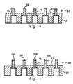
- the substrate 88 is then etched to remove a portion of either the top surface 90 or the bottom surface 92 of the substrate 88 , as illustrated in FIG. 10 .
- the substrate 88 is etched to a depth D 4 , as illustrated in FIG. 10 , of between 50 and 500 microns, and more preferably, a depth of at most 150 microns.
- Various types of etching may be used to remove a portion of the substrate 88 , such as wet etching with ethylene diamine pyrocatechol or potassium hydroxide, or dry etching.
- the top surface 90 is etched to remove a portion of the substrate 88 and create an etched surface 91 which is closer to the bottom surface 92 than the original top surface 90 .
Abstract
Description
Claims (17)
Priority Applications (3)
Application Number | Priority Date | Filing Date | Title |
---|---|---|---|
US10/429,333 US7217396B2 (en) | 2003-05-05 | 2003-05-05 | Microfabricated micro fluid channels |
PCT/US2004/013974 WO2004103886A2 (en) | 2003-05-05 | 2004-05-05 | Microfabricated micro fluid channels |
US11/682,687 US7737045B2 (en) | 2003-05-05 | 2007-03-06 | Microfabricated micro fluid channels |
Applications Claiming Priority (1)
Application Number | Priority Date | Filing Date | Title |
---|---|---|---|
US10/429,333 US7217396B2 (en) | 2003-05-05 | 2003-05-05 | Microfabricated micro fluid channels |
Related Child Applications (1)
Application Number | Title | Priority Date | Filing Date |
---|---|---|---|
US11/682,687 Division US7737045B2 (en) | 2003-05-05 | 2007-03-06 | Microfabricated micro fluid channels |
Publications (2)
Publication Number | Publication Date |
---|---|
US20040223886A1 US20040223886A1 (en) | 2004-11-11 |
US7217396B2 true US7217396B2 (en) | 2007-05-15 |
Family
ID=33416019
Family Applications (2)
Application Number | Title | Priority Date | Filing Date |
---|---|---|---|
US10/429,333 Expired - Lifetime US7217396B2 (en) | 2003-05-05 | 2003-05-05 | Microfabricated micro fluid channels |
US11/682,687 Expired - Fee Related US7737045B2 (en) | 2003-05-05 | 2007-03-06 | Microfabricated micro fluid channels |
Family Applications After (1)
Application Number | Title | Priority Date | Filing Date |
---|---|---|---|
US11/682,687 Expired - Fee Related US7737045B2 (en) | 2003-05-05 | 2007-03-06 | Microfabricated micro fluid channels |
Country Status (2)
Country | Link |
---|---|
US (2) | US7217396B2 (en) |
WO (1) | WO2004103886A2 (en) |
Cited By (8)
Publication number | Priority date | Publication date | Assignee | Title |
---|---|---|---|---|
US20040228962A1 (en) * | 2003-05-16 | 2004-11-18 | Chang Liu | Scanning probe microscopy probe and method for scanning probe contact printing |
US20070062264A1 (en) * | 2005-09-21 | 2007-03-22 | Xuefeng Wang | Multifunctional probe array system |
US20070163647A1 (en) * | 2003-05-05 | 2007-07-19 | Chang Liu | Microfabricated micro fluid channels |
WO2011130446A1 (en) | 2010-04-14 | 2011-10-20 | Nanoink, Inc. | Improved cantilevers for deposition |
WO2011133663A1 (en) | 2010-04-20 | 2011-10-27 | Nanoink, Inc. | Functionalizing biosensors using a multiplexed dip pen array |
US20120052240A1 (en) * | 2009-05-15 | 2012-03-01 | Takashi Washizu | Microchip |
WO2013061199A1 (en) * | 2011-10-25 | 2013-05-02 | International Business Machines Corporation | Microfluidic device with interconnects |
WO2013067395A2 (en) | 2011-11-04 | 2013-05-10 | Nanoink, Inc. | Method and apparatus for improving ink deposition |
Families Citing this family (8)
Publication number | Priority date | Publication date | Assignee | Title |
---|---|---|---|---|
WO2004044552A2 (en) * | 2002-11-12 | 2004-05-27 | Nanoink, Inc. | Methods and apparatus for ink delivery to nanolithographic probe systems |
CN1883234A (en) * | 2003-11-21 | 2006-12-20 | 皇家飞利浦电子股份有限公司 | Display panel |
EP1748846B1 (en) * | 2004-04-30 | 2015-04-01 | Bioforce Nanosciences, Inc. | Method and apparatus for depositing material onto a surface |
US20100261286A1 (en) * | 2005-07-14 | 2010-10-14 | Young Hoon Kim | Microfluidic devices and methods of preparing and using the same |
US8124030B2 (en) * | 2007-05-08 | 2012-02-28 | The Regents Of The University Of California | Microfluidic device having regulated fluid transfer between elements located therein |
US8740209B2 (en) * | 2012-02-22 | 2014-06-03 | Expresslo Llc | Method and apparatus for ex-situ lift-out specimen preparation |
CN108878690B (en) * | 2018-07-02 | 2020-04-28 | 京东方科技集团股份有限公司 | Manufacturing method of display substrate and display device |
JP7246041B2 (en) * | 2018-11-07 | 2023-03-27 | ウシオ電機株式会社 | CELL CULTURE CHIP AND MANUFACTURING METHOD THEREOF |
Citations (12)
Publication number | Priority date | Publication date | Assignee | Title |
---|---|---|---|---|
US6284113B1 (en) | 1997-09-19 | 2001-09-04 | Aclara Biosciences, Inc. | Apparatus and method for transferring liquids |
US20010020588A1 (en) * | 1997-09-15 | 2001-09-13 | Whitehead Institute For Biomedical Research | Methods and apparatus for processing a sample of biomolecular analyte using a microfabricated device |
US20010036674A1 (en) | 2000-02-23 | 2001-11-01 | Indermuhle Pierre F. | Chips having elevated sample surfaces |
US20020025279A1 (en) * | 2000-05-24 | 2002-02-28 | Weigl Bernhard H. | Capillaries for fluid movement within microfluidic channels |
US6409900B1 (en) | 1996-04-16 | 2002-06-25 | Caliper Technologies Corp. | Controlled fluid transport in microfabricated polymeric substrates |
US6429025B1 (en) | 1996-06-28 | 2002-08-06 | Caliper Technologies Corp. | High-throughput screening assay systems in microscale fluidic devices |
US20020123153A1 (en) | 1998-09-17 | 2002-09-05 | Moon James E. | Integrated monolithic microfabricated electrospray and liquid chromatography system and method |
US20030017077A1 (en) * | 2001-07-18 | 2003-01-23 | Pohang University Of Science And Technology Foundation | Sample clean-up apparatus for mass spectrometry |
US20030026740A1 (en) * | 2001-08-06 | 2003-02-06 | Staats Sau Lan Tang | Microfluidic devices |
US6555389B1 (en) * | 1999-05-11 | 2003-04-29 | Aclara Biosciences, Inc. | Sample evaporative control |
US20030082080A1 (en) * | 1999-10-01 | 2003-05-01 | Agilent Technologies, Inc. | Coupling to microstructures for a laboratory microchip |
US20040018116A1 (en) * | 2002-07-26 | 2004-01-29 | Desmond Sean M. | Microfluidic size-exclusion devices, systems, and methods |
Family Cites Families (26)
Publication number | Priority date | Publication date | Assignee | Title |
---|---|---|---|---|
US5221415A (en) * | 1989-01-17 | 1993-06-22 | Board Of Trustees Of The Leland Stanford Junior University | Method of forming microfabricated cantilever stylus with integrated pyramidal tip |
US5053100A (en) * | 1989-09-01 | 1991-10-01 | Microfab Technologies, Inc. | Method of making apparatus for dispensing small amounts of fluids |
ATE186151T1 (en) * | 1991-07-17 | 1999-11-15 | Canon Kk | INFORMATION RECORDING/REPRODUCING DEVICE FOR RECORDING AND/OR REPRODUCING INFORMATION TO/FROM AN INFORMATION RECORDING MEDIUM BY USING A PROBE. |
US5514501A (en) * | 1994-06-07 | 1996-05-07 | The United States Of America As Represented By The Secretary Of Commerce | Process for UV-photopatterning of thiolate monolayers self-assembled on gold, silver and other substrates |
US5751683A (en) * | 1995-07-24 | 1998-05-12 | General Nanotechnology, L.L.C. | Nanometer scale data storage device and associated positioning system |
US6353219B1 (en) * | 1994-07-28 | 2002-03-05 | Victor B. Kley | Object inspection and/or modification system and method |
US5883387A (en) * | 1994-11-15 | 1999-03-16 | Olympus Optical Co., Ltd. | SPM cantilever and a method for manufacturing the same |
JP3679519B2 (en) | 1995-09-14 | 2005-08-03 | キヤノン株式会社 | Manufacturing method of micro tip for detecting tunnel current or micro force or magnetic force, manufacturing method of probe having the micro tip, probe thereof, probe unit having the probe, scanning probe microscope, and information recording / reproducing apparatus |
ZA975891B (en) * | 1996-07-05 | 1998-07-23 | Combimatrix Corp | Electrochemical solid phase synthesis of polymers |
US5922214A (en) * | 1997-01-17 | 1999-07-13 | Wayne State University | Nanometer scale fabrication method to produce thin film nanostructures |
JP3697034B2 (en) * | 1997-08-26 | 2005-09-21 | キヤノン株式会社 | Method of manufacturing protrusions having minute openings, and probes or multiprobes using them |
DE69900384T2 (en) * | 1998-04-28 | 2003-02-27 | Nano World Ag Neuchatel | COST-EFFECTIVE MICROBIAL BEAM OF PHOTOPLASTIC MATERIAL |
US6635311B1 (en) | 1999-01-07 | 2003-10-21 | Northwestern University | Methods utilizing scanning probe microscope tips and products therefor or products thereby |
US6827979B2 (en) * | 1999-01-07 | 2004-12-07 | Northwestern University | Methods utilizing scanning probe microscope tips and products therefor or produced thereby |
US6642129B2 (en) * | 2001-07-26 | 2003-11-04 | The Board Of Trustees Of The University Of Illinois | Parallel, individually addressable probes for nanolithography |
EP1359388B1 (en) | 2002-05-03 | 2004-12-08 | Nanoworld AG | SPM sensor and method for producing the same |
US7241420B2 (en) | 2002-08-05 | 2007-07-10 | Palo Alto Research Center Incorporated | Capillary-channel probes for liquid pickup, transportation and dispense using stressy metal |
JP2006504136A (en) * | 2002-10-21 | 2006-02-02 | ナノインク インコーポレーティッド | Nanometer scale design structure, manufacturing method and apparatus thereof, mask repair, reinforcement, and application to manufacturing |
WO2004044552A2 (en) * | 2002-11-12 | 2004-05-27 | Nanoink, Inc. | Methods and apparatus for ink delivery to nanolithographic probe systems |
KR20040105278A (en) * | 2003-06-04 | 2004-12-16 | 현대자동차주식회사 | Composition of cast iron for engine exhaust system in automobile |
US6943417B2 (en) * | 2003-05-01 | 2005-09-13 | Clemson University | DNA-based memory device and method of reading and writing same |
US7217396B2 (en) | 2003-05-05 | 2007-05-15 | The Board Of Trustees Of The University Of Illinois | Microfabricated micro fluid channels |
US20040228962A1 (en) * | 2003-05-16 | 2004-11-18 | Chang Liu | Scanning probe microscopy probe and method for scanning probe contact printing |
US7167435B2 (en) * | 2004-03-09 | 2007-01-23 | Hewlett-Packard Development Company, L.P. | Storage device having a probe with plural tips |
US20050236566A1 (en) | 2004-04-26 | 2005-10-27 | Chang Liu | Scanning probe microscope probe with integrated capillary channel |
US7281419B2 (en) | 2005-09-21 | 2007-10-16 | The Board Of Trustees Of The University Of Illinois | Multifunctional probe array system |
-
2003
- 2003-05-05 US US10/429,333 patent/US7217396B2/en not_active Expired - Lifetime
-
2004
- 2004-05-05 WO PCT/US2004/013974 patent/WO2004103886A2/en active Application Filing
-
2007
- 2007-03-06 US US11/682,687 patent/US7737045B2/en not_active Expired - Fee Related
Patent Citations (12)
Publication number | Priority date | Publication date | Assignee | Title |
---|---|---|---|---|
US6409900B1 (en) | 1996-04-16 | 2002-06-25 | Caliper Technologies Corp. | Controlled fluid transport in microfabricated polymeric substrates |
US6429025B1 (en) | 1996-06-28 | 2002-08-06 | Caliper Technologies Corp. | High-throughput screening assay systems in microscale fluidic devices |
US20010020588A1 (en) * | 1997-09-15 | 2001-09-13 | Whitehead Institute For Biomedical Research | Methods and apparatus for processing a sample of biomolecular analyte using a microfabricated device |
US6284113B1 (en) | 1997-09-19 | 2001-09-04 | Aclara Biosciences, Inc. | Apparatus and method for transferring liquids |
US20020123153A1 (en) | 1998-09-17 | 2002-09-05 | Moon James E. | Integrated monolithic microfabricated electrospray and liquid chromatography system and method |
US6555389B1 (en) * | 1999-05-11 | 2003-04-29 | Aclara Biosciences, Inc. | Sample evaporative control |
US20030082080A1 (en) * | 1999-10-01 | 2003-05-01 | Agilent Technologies, Inc. | Coupling to microstructures for a laboratory microchip |
US20010036674A1 (en) | 2000-02-23 | 2001-11-01 | Indermuhle Pierre F. | Chips having elevated sample surfaces |
US20020025279A1 (en) * | 2000-05-24 | 2002-02-28 | Weigl Bernhard H. | Capillaries for fluid movement within microfluidic channels |
US20030017077A1 (en) * | 2001-07-18 | 2003-01-23 | Pohang University Of Science And Technology Foundation | Sample clean-up apparatus for mass spectrometry |
US20030026740A1 (en) * | 2001-08-06 | 2003-02-06 | Staats Sau Lan Tang | Microfluidic devices |
US20040018116A1 (en) * | 2002-07-26 | 2004-01-29 | Desmond Sean M. | Microfluidic size-exclusion devices, systems, and methods |
Non-Patent Citations (8)
Title |
---|
Baldock et al., "Microfabricated Devices for Chemical and Biochemical Analysis Systems," Department of Instrumentation and Analytical Science, Manchester, United Kingdom, 1 page. |
International Search Report dated Nov. 30, 2005 for corresponding PCT application No. PCT/US04/13974. |
Kirk-Othmer, "Integrated Circuits," Encyclopedia of Chemical Technology, 1995, pp. 677-709, vol. 14. |
Niklaus et al., "Void-Free Full Wafer Adhesive Bonding," Department of Signals, Sensors and Systems, Royal Institute of Technology, Stockholm, Sweden, 6 pages. |
Piner, et al., "'Dip-Pen" Nanolithography,' Jan. 29, 1999, Science, 283, 661-663. * |
Van Zant, "Semiconductor Devices and Integrated Circuit Formation," Microchip Fabrication: A Practical Guide to Semiconductor Processing, 2000, pp. 491-527, Chapter 16. |
Zou, et al., "A mould-and-transfer technology for fabricating scanning probe microscopy probes," Oct. 15, 2003, Institute of Physics Publishing, Journal of Micromechanics and Microenginneering, 14, 204-211. * |
Cited By (16)
Publication number | Priority date | Publication date | Assignee | Title |
---|---|---|---|---|
US20070163647A1 (en) * | 2003-05-05 | 2007-07-19 | Chang Liu | Microfabricated micro fluid channels |
US7737045B2 (en) | 2003-05-05 | 2010-06-15 | The Board Of Trustees Of The University Of Illinois | Microfabricated micro fluid channels |
US20040228962A1 (en) * | 2003-05-16 | 2004-11-18 | Chang Liu | Scanning probe microscopy probe and method for scanning probe contact printing |
US20070062264A1 (en) * | 2005-09-21 | 2007-03-22 | Xuefeng Wang | Multifunctional probe array system |
US7281419B2 (en) | 2005-09-21 | 2007-10-16 | The Board Of Trustees Of The University Of Illinois | Multifunctional probe array system |
US20070289369A1 (en) * | 2005-09-21 | 2007-12-20 | Xuefeng Wang | Multifunctional probe array system |
US7523650B2 (en) | 2005-09-21 | 2009-04-28 | The Board Of Trustees Of The University Of Illinois | Multifunctional probe array system |
US9238224B2 (en) * | 2009-05-15 | 2016-01-19 | Konica Minolta, Inc. | Microchip |
US20120052240A1 (en) * | 2009-05-15 | 2012-03-01 | Takashi Washizu | Microchip |
WO2011130446A1 (en) | 2010-04-14 | 2011-10-20 | Nanoink, Inc. | Improved cantilevers for deposition |
WO2011133663A1 (en) | 2010-04-20 | 2011-10-27 | Nanoink, Inc. | Functionalizing biosensors using a multiplexed dip pen array |
GB2509440A (en) * | 2011-10-25 | 2014-07-02 | Ibm | Microfluidic device with interconnects |
GB2509440B (en) * | 2011-10-25 | 2015-06-03 | Ibm | Microfluidic device with interconnects |
US9205397B2 (en) | 2011-10-25 | 2015-12-08 | International Business Machines Corporation | Microfluidic device with interconnects |
WO2013061199A1 (en) * | 2011-10-25 | 2013-05-02 | International Business Machines Corporation | Microfluidic device with interconnects |
WO2013067395A2 (en) | 2011-11-04 | 2013-05-10 | Nanoink, Inc. | Method and apparatus for improving ink deposition |
Also Published As
Publication number | Publication date |
---|---|
WO2004103886A2 (en) | 2004-12-02 |
US20040223886A1 (en) | 2004-11-11 |
WO2004103886A3 (en) | 2006-04-06 |
US20070163647A1 (en) | 2007-07-19 |
US7737045B2 (en) | 2010-06-15 |
Similar Documents
Publication | Publication Date | Title |
---|---|---|
US7737045B2 (en) | Microfabricated micro fluid channels | |
US6851846B2 (en) | Mixing method, mixing structure, micromixer and microchip having the mixing structure | |
US7458661B2 (en) | Method and apparatus for promoting the complete transfer of liquid drops from a nozzle | |
EP2429697B1 (en) | Multilayer microfluidic probe head | |
JP4672142B2 (en) | Silicon microfabricated protrusions with ducts | |
WO2001033614A1 (en) | Method for fabricating arrays of micro-needles | |
EP1114314B1 (en) | Device comprising a plurality of analysis sites on a support and method of manufacturing the device | |
US20050282221A1 (en) | Process for manufacturing a microfluidic device with buried channels | |
US9745949B2 (en) | Multilayer microfluidic probe head with immersion channels and fabrication thereof | |
US20030213918A1 (en) | Electrospray emitter for microfluidic channel | |
US8728988B2 (en) | Probe array base, method for manufacturing probe array base, method for manufacturing probe array | |
JP2003039396A (en) | Method of manufacturing for microstructure for microfluidic application and method of manufacturing for fluidic device | |
CN104043490A (en) | Method and system for manufacturing integrated fluidic chips | |
US7824630B2 (en) | DNA probe synthesis on chip on demand by mems ejector array | |
US9917148B2 (en) | Self-limited, anisotropic wet etching of transverse vias in microfluidic chips | |
US9564386B2 (en) | Semiconductor package with structures for cooling fluid retention | |
US20220347681A1 (en) | Microfluidic chips with one or more vias filled with sacrificial plugs | |
US11458474B2 (en) | Microfluidic chips with one or more vias | |
JP2003024753A (en) | Microextractor | |
WO2007087449A2 (en) | Fluid transfer and printing devices | |
WO2002041996A1 (en) | Inlet for microfluidic devices | |
US11351539B2 (en) | Multilevel microfluidic device | |
NL2026627B1 (en) | A MEMS device for transmission microscopy, and a method | |
CN112169851B (en) | Micro-channel inlet cover plate and preparation and use methods thereof | |
CN1920560A (en) | Chips for biological or chemical analysis, apparatus and method for processing fluid |
Legal Events
Date | Code | Title | Description |
---|---|---|---|
AS | Assignment |
Owner name: ILLINOIS, UNIVERSITY OF, ILLINOIS Free format text: ASSIGNMENT OF ASSIGNORS INTEREST;ASSIGNORS:LIU, CHANG;RYU, KEE;BULLEN, DAVID;REEL/FRAME:014040/0090;SIGNING DATES FROM 20030409 TO 20030410 |
|
AS | Assignment |
Owner name: AIR FORCE, UNITED STATES, VIRGINIA Free format text: CONFIRMATORY LICENSE;ASSIGNOR:UNIVERSITY OF ILLINOIS AT URBANA-CHAMPAIGN;REEL/FRAME:016220/0216 Effective date: 20030904 |
|
STCF | Information on status: patent grant |
Free format text: PATENTED CASE |
|
FPAY | Fee payment |
Year of fee payment: 4 |
|
FPAY | Fee payment |
Year of fee payment: 8 |
|
MAFP | Maintenance fee payment |
Free format text: PAYMENT OF MAINTENANCE FEE, 12TH YR, SMALL ENTITY (ORIGINAL EVENT CODE: M2553); ENTITY STATUS OF PATENT OWNER: SMALL ENTITY Year of fee payment: 12 |