US7221089B2 - Organic light emitting diode display device and method of manufacturing the same - Google Patents
Organic light emitting diode display device and method of manufacturing the same Download PDFInfo
- Publication number
- US7221089B2 US7221089B2 US10/652,549 US65254903A US7221089B2 US 7221089 B2 US7221089 B2 US 7221089B2 US 65254903 A US65254903 A US 65254903A US 7221089 B2 US7221089 B2 US 7221089B2
- Authority
- US
- United States
- Prior art keywords
- light emitting
- emitting diode
- organic light
- layer
- protective layer
- Prior art date
- Legal status (The legal status is an assumption and is not a legal conclusion. Google has not performed a legal analysis and makes no representation as to the accuracy of the status listed.)
- Expired - Fee Related, expires
Links
Images


Classifications
-
- H—ELECTRICITY
- H10—SEMICONDUCTOR DEVICES; ELECTRIC SOLID-STATE DEVICES NOT OTHERWISE PROVIDED FOR
- H10K—ORGANIC ELECTRIC SOLID-STATE DEVICES
- H10K50/00—Organic light-emitting devices
- H10K50/80—Constructional details
- H10K50/84—Passivation; Containers; Encapsulations
- H10K50/844—Encapsulations
-
- H—ELECTRICITY
- H10—SEMICONDUCTOR DEVICES; ELECTRIC SOLID-STATE DEVICES NOT OTHERWISE PROVIDED FOR
- H10K—ORGANIC ELECTRIC SOLID-STATE DEVICES
- H10K59/00—Integrated devices, or assemblies of multiple devices, comprising at least one organic light-emitting element covered by group H10K50/00
- H10K59/10—OLED displays
- H10K59/12—Active-matrix OLED [AMOLED] displays
- H10K59/122—Pixel-defining structures or layers, e.g. banks
-
- H—ELECTRICITY
- H10—SEMICONDUCTOR DEVICES; ELECTRIC SOLID-STATE DEVICES NOT OTHERWISE PROVIDED FOR
- H10K—ORGANIC ELECTRIC SOLID-STATE DEVICES
- H10K59/00—Integrated devices, or assemblies of multiple devices, comprising at least one organic light-emitting element covered by group H10K50/00
- H10K59/80—Constructional details
- H10K59/87—Passivation; Containers; Encapsulations
- H10K59/873—Encapsulations
-
- H—ELECTRICITY
- H10—SEMICONDUCTOR DEVICES; ELECTRIC SOLID-STATE DEVICES NOT OTHERWISE PROVIDED FOR
- H10K—ORGANIC ELECTRIC SOLID-STATE DEVICES
- H10K59/00—Integrated devices, or assemblies of multiple devices, comprising at least one organic light-emitting element covered by group H10K50/00
- H10K59/10—OLED displays
- H10K59/12—Active-matrix OLED [AMOLED] displays
- H10K59/123—Connection of the pixel electrodes to the thin film transistors [TFT]
Definitions
- the present invention relates to an organic light emitting diode display device including organic light emitting diode elements as light emission elements, and each of the organic light emitting diode elements is covered with a protective layer. More specifically, the present invention relates to the organic light emitting diode display device having a stress relaxation layer for relaxing a stress caused by the protective layer, and a method of manufacturing the organic light emitting diode display device.
- Organic light emitting diode displays are now attracting attention as candidates for flat display devices instead of liquid crystal displays.
- the organic light emitting diode displays differ from the liquid crystal displays in that organic light emitting diode elements generating light are employed. In other words, the organic light emitting diode displays do not require backlight which the liquid crystal displays need.
- An organic light emitting diode element has high speed response, high contrast, and high visibility. Further, an organic light emitting diode display using the organic light emitting diode element has a relatively simple structure, which is advantageous in view of manufacturing cost.
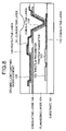
- FIG. 8 is a sectional view of a display cell of a conventional organic light emitting diode display.
- a thin film transistor 102 serving as a switching element, a thin film transistor 103 serving as a driver element, and a conductive layer 110 are formed on a substrate 101 .
- a planarizing layer 104 is formed to cover the substrate 101 , and the thin film transistors 102 and 103 .
- An organic light emitting diode element 105 , and conductive layers 106 and 107 are formed on the planarizing layer 104 so that the organic light emitting diode element 105 is located between the conductive layers 106 and 107 .
- the conductive layer 107 is electrically connected to the thin film transistor 103 via conductive layers 108 and 110 .
- the organic light emitting diode element 105 is electrically connected to and controlled by the thin film transistors 102 and 103 .
- a protective layer 109 is deposited on the uppermost layer as shown FIG. 8 .
- Such a protective layer is disclosed in, for example, “A 13.0-inch AM-OLED display with top emitting structure and adaptive current mode programmed pixel circuit”, T. Sasaoka et al, SID Tech. Dig., 2001, pp. 384 to 387.
- the organic light emitting diode element 105 has a structure similar to that of a light emitting diode, including at least one of a hole transport layer and an electron transport layer, and an emitting layer.
- These hole transport layer, the electron transport layer, and the emitting layer are made of organic materials such as diamine compounds, quinolinol aluminum complex, and phthalocyanine. Some carbon-carbon conjugated bonds of these materials are easily separated by moisture or oxygen. Separating of the carbon-carbon conjugated bonds causes electrical conductivity to decrease. Therefore, the organic light emitting diode display has a sealing structure for protecting the surface of the organic light emitting diode elements from air.
- the organic light emitting diode display is protected from air with a glass substrate separated from the surface of the organic light emitting diode elements by spacers.
- the glass substrate causes various problems such as occurrence of optical loss.
- light emitted from the organic light emitting diode element is reflected by the glass surface, and weight and thickness of the organic light emitting diode display increases in addition to an increase in the cost of the glass substrate. Therefore, using the protective layer 109 made of silicon nitride (hereinafter, “SiN x ”) having excellent light transmission characteristics, instead of the glass substrate, is desired.
- the protective layer has a problem in which the protective layer located on the surface of the organic light emitting diode display causes a tensile stress.
- the tensile stress causes separation of the protective layer or substrate crack.
- the material of the organic light emitting diode element is weak against a high temperature, and the glass transition occurs at a temperature as low as about 120 degrees centigrade. Therefore, depositing the protective layer requires the temperature condition not higher than the glass-transition temperature, more specifically, from about 80 to about 120 degrees centigrade.
- SiN x it is common to deposit SiN x at a temperature of from 250 to 300 degrees centigrade, and preferably about 280 degrees centigrade.
- the SiN x layer deposited under a temperature of from about 80 to about 120 degrees centigrade has a lower density.
- the lower density leads to strong interatomic force.
- an influence of stress to the organic light emitting diode elements increases as compared with the normal layer structure.
- the protective layer needs to have a certain thickness, specifically, a thickness of from 1 to 3 micrometers.
- a thickness of from 1 to 3 micrometers the tensile stress on the surface of the organic light emitting diode elements becomes a serious problem.
- the protective layer not limited to the SiN x layer, potentially has the problem of the stress. Therefore, in the general organic light emitting diode display which has the sealing structure with the protective layer, it is desired to decrease the stress caused by the protective layer.
- the organic light emitting diode display device includes an organic light emitting diode element; a protective layer covering the organic light emitting diode element; and a stress relaxation layer adjacent to sides of the protective layer, for relaxing a stress caused by the protective layer.
- the organic light emitting diode display device includes a plurality of organic light emitting diode elements that are arranged in a matrix; a plurality of protective layers, each of the protective layers covering at least one of the organic light emitting diode elements; and a stress relaxation layer that is formed between the protective layers, for relaxing a stress caused by the protective layers.
- the method of manufacturing an organic light emitting diode display device includes forming on a substrate thin film transistors for driving an organic light emitting diode element; forming an insulating layer to cover the thin film transistors; forming a stress relaxation layer to surround area where a protective layer is formed, for relaxing a stress caused by the protective layer; forming an organic light emitting diode element on a part of the area; and forming the protective layer on the area to cover the organic light emitting diode element.
- FIG. 1 is a top view of an organic light emitting diode display device according to one embodiment
- FIG. 2 is a sectional view of a display cell of the organic light emitting diode display device
- FIG. 3 is a schematic perspective view illustrating arrangement of a protective layer and a stress relaxation layer in the organic light emitting diode display device
- FIG. 4 is an equivalent circuit diagram of the display cell of the organic light emitting diode display device
- FIGS. 5A and 5B are diagrams for explaining a stress caused by the protective layer to the array substrate
- FIGS. 6A to 6C are sectional views indicating a manufacturing process of the organic light emitting diode display device
- FIGS. 7A to 7C are sectional views indicating a manufacturing process of the organic light emitting diode display device.
- FIG. 8 is a sectional view of a display cell of a conventional organic light emitting diode display.
- the organic light emitting diode display device uses an organic light emitting diode element as a light emission element, and has a structure in which the protective layer for protecting the organic light emitting diode element from air is divided by a layer structure made of a material different from that of the protective layer and serving as a stress relaxation layer.
- FIG. 1 is a top view of the structure of an organic light emitting diode display device according to one embodiment.
- the organic light emitting diode display device includes a data line driving circuit 1 arranged on an array substrate or within the array substrate, a plurality of data lines 2 extended from the data line driving circuit 1 , a scan line driving circuit 3 , a plurality of scan lines 4 extended from the scan line driving circuit 3 , and a display area 5 in which the organic light emitting diode elements are arranged in a matrix on the array substrate corresponding to pixels.
- a protective layer 6 for protecting the organic light emitting diode element from air, and a stress relaxation layer 7 arranged to divide the protective layer 6 into a plurality of areas are provided on the array substrate.
- the data line driving circuit 1 is for supplying a display signal to the display area 5 via the data line 2 .
- the scan line driving circuit 3 is for supplying a scan signal to the display area 5 via the scan line 4 .
- the display area 5 is for displaying images based on the supplied display signal and scan signal.
- the display area 5 has the organic light emitting diode elements arranged corresponding to pixels and predetermined circuit elements arranged corresponding to the organic light emitting diode elements, and the circuit elements control predetermined electric current based on the display signal and the scan signal to control the emitting state of the organic light emitting diode elements, thereby displaying an image as a whole.
- FIG. 2 is a sectional view of the structure in the display area 5 of the organic light emitting diode display.
- thin film transistors 9 and 10 are arranged on a substrate 8 , and a conductive layer 11 for contacting the thin film transistors 9 and 10 , and a conductive layer 12 for contacting the thin film transistors 9 and 10 with the organic light emitting diode element 16 are arranged thereon.
- a planarizing layer 13 made of a polymer or the like is laminated on the surface of the substrate 8 , and on the thin film transistors 9 and 10 , and the conductive layers 11 and 12 , excluding a part of the area on the conductive layer 12 . Further, a conductive layer 14 extended from a power line is arranged on the planarizing layer 13 , and the organic light emitting diode element 16 is arranged on a part of the area of the conductive layer 14 .
- a conductive layer 17 is arranged on the organic light emitting diode element 16 , and the conductive layer 17 has a structure of extending horizontally from the organic light emitting diode element 16 , and being contacted to the conductive layer 12 via the conductive layer 15 .
- the thin film transistors 9 and 10 function as a switching element and a driver element, respectively, with respect to the organic light emitting diode element 16 .
- the thin film transistor 9 is connected to predetermined data line and scan line, to control the emitting state of the organic light emitting diode element 16 based on the display signal and the scan signal supplied via the data line and the scan line.
- the specific connection mode of the thin film transistors 9 and 10 , the data line, the scan line, and the organic light emitting diode element 16 will be explained later.
- the organic light emitting diode element 16 functions as a light emission element.
- the organic light emitting diode element 16 has a structure having at least one of a hole transport layer and an electron transport layer, and an emitting layer, so as to emit light by radiative recombination of a hole and an electron injected into the emitting layer.
- the hole transport layer, the electron transport layer, and the emitting layer are made of organic materials such as diamine compounds, quinolinol aluminum complex, and phthalocyanine, and have a structure in which predetermined impurities are added according to need.
- the protective layer 6 is for covering the organic light emitting diode element 16 from the outside air.
- moisture, oxygen, and the like contained in air adhere to the organic light emitting diode element 16 , carbon-carbon conjugated bond of the organic light emitting diode element 16 is separated, and therefore electrical conductivity of the organic light emitting diode element 16 is decreased.
- the protective layer 6 is formed to cover the whole organic light emitting diode element 16 .
- the protective layer 6 is made of a material having excellent light transmission characteristics, in order to output light emitted from the organic light emitting diode element 16 to the outside.
- the organic light emitting diode display according to the embodiment has a structure such that the organic light emitting diode element 16 functions as a light emission element, and emits light vertically upwards with respect to the array substrate 18 . Therefore, the protective layer 6 located vertically upwards with respect to the organic light emitting diode element 16 needs to have excellent light transmission characteristics, in order to prevent the transmission of light emitted from the organic light emitting diode element 16 from being hindered.
- a material having such characteristics for example, SiN x is used. SiN x herein is not constituted only of Si atoms and N atoms, but may contain predetermined impurities, for example, impurities such as hydrogen, oxygen, and the like are mixed at a certain ratio.
- the stress relaxation layer 7 is for relaxing the intensity of stress applied to the array substrate 18 by the protective layer 6 .
- the stress relaxation layer 7 is arranged to divide the area where the protective layer 6 is arranged into a plurality of areas.
- a photoresist is used in the embodiment. This is because the stress relaxation layer 7 having a desired pattern can be easily formed by using a photolithographic technique or the like.
- the photoresist is used from a standpoint that it also serves as a mask.
- the photoresist since the photoresist has poor light transmission characteristics, it is desired to arrange the photoresist at a position where the light emitted from the organic light emitting diode element 16 is not hindered. Further, a dielectric layer 24 formed at the time of forming the protective layer 6 exists on the stress relaxation layer 7 .
- the stress relaxation layer 7 separates the dielectric layer 24 from the protective layer 6 , so that adjacent protective layers 6 are not contacted to each other via the dielectric layer 24 . Since the dielectric layer 24 does not have an important function in the embodiment, it is omitted in FIG. 1 , and will be omitted in other figures appropriately for convenience sake of explanation. Since the dielectric layer 24 does not have a characteristic function in the organic light emitting diode display according to the embodiment, the dielectric layer 24 may be removed at the time of manufacturing.
- FIG. 3 is a schematic perspective view of the specific structure of the protective layer 6 and the stress relaxation layer 7 deposited on the surface of the array substrate.
- the sectional structure of the stress relaxation layer 7 has a trapezoidal shape, with the top width of the trapezoid larger than the base width.
- Such a structure can be realized, for example, by using a predetermined photoresist for a material forming the stress relaxation layer 7 , and optimizing the heating temperature.
- FIG. 4 is a diagram indicating an equivalent circuit in a part of a display cell of the organic light emitting diode display device.
- the organic light emitting diode element 16 and the thin film transistor 9 are connected to each other via one of the source and drain electrodes, and functions as a driver element, which controls the emitting state of the organic light emitting diode element 16 .
- the thin film transistor 10 is connected to the gate electrode of the thin film transistor 9 via the other of the source and drain electrodes, and functions as a switching element.
- the gate electrode of the thin film transistor 9 is connected to the scan line 4 , and the other of the source and drain electrodes is connected to the data line 2 .
- the organic light emitting diode element 16 is connected to the power line 20 , and a capacitor 19 is arranged between the other of the source and drain electrodes of the thin film transistor 9 and the power line 20 .
- the protective layer 6 is arranged in a physically separated state on the area separated by the stress relaxation layer 7 , not in an integrally deposited state on the surface of the array substrate. Therefore, the area in which the respective protective layers 6 separated by the stress relaxation layer 7 come in contact with the array substrate is smaller than the area when the stress relaxation layer 7 is not provided.
- FIG. 5A is a diagram for explaining a stress generated in a structure in which the stress relaxation layer 7 is not provided, for a comparison
- FIG. 5B is a diagram for explaining changes in the stress by providing the stress relaxation layer 7 .
- the protective layer 6 ′ is integrally arranged on the array substrate 18 ′, and hence the stress applied by the protective layer 6 ′ is large as shown by the arrows in FIG. 5A .
- the protective layer 6 is arranged on the array substrate 18 , with the protective layer 6 separated into a plurality of areas by the stress relaxation layer 7 . Therefore, the area in which the individual protective layer 6 comes in contact with the array substrate 18 is small as compared with FIG. 5A , and it is obvious that the length of the stress in the application direction becomes short.
- the stress changes according to the contact area and the length of stress in the application direction. Therefore, in the organic light emitting diode display according to the embodiment, the stress applied to the array substrate 18 becomes smaller than the case of FIG. 5A , and hence the influence of the stress with respect to the array substrate 18 is relaxed. As a result, there is an advantage in that even when the protective layer 6 is made of, for example, SiN x film-formed at a low temperature, peeling of the protective layer 6 and cracks in the array substrate 18 , which occur in the conventional structure, can be suppressed. Further, by relaxing the stress due to the protective layer 6 by the stress relaxation layer 7 , the protective layer 6 itself can be prevented from being damaged in the crystalline structure by the stress, to decrease the covering property against the outside air.
- the contact area with the array substrate 18 and the horizontal sectional shape of the individual protective layer 6 separated by the stress relaxation layer 7 are the same. Therefore, the stress applied by the individual protective layer 6 with respect to the array substrate 18 becomes equal, thereby having an advantage in that the stress does not concentrate in a specific area of the array substrate 18 .
- FIGS. 6A to 6C and FIGS. 7A to 7C indicate the manufacturing method of the organic light emitting diode display according to the embodiment. The manufacturing method will be explained below with reference to these figures.
- the thin film transistors 9 and 10 form the thin film transistors 9 and 10 , the conductive layer 11 for connecting the thin film transistors 9 and 10 , and the conductive layer 12 for connecting the thin film transistor 10 and the organic light emitting diode element 16 on the nonconductive substrate 8 according to a predetermined process.
- an insulating material such as polymers, SiN x , or the like, form a contact hole on a part of the area on the conductive layer 12 .
- the organic light emitting diode element has not yet been formed.
- the planarizing layer 13 can be formed at a high temperature, and the formed planarizing layer 13 does not cause a stress problem. Then deposit conductive layers 14 and 15 having a predetermined pattern on the planarizing layer 13 , and deposit thereon an insulating layer 23 that electrically separates the conductive layer 17 formed later from the conductive layer 14 and prevents the organic light emitting diode element 16 from being cut. As a result, the structure shown in FIG. 6A is formed.
- the stress relaxation layer 7 Thereafter, form the stress relaxation layer 7 .
- the stress relaxation layer 7 having a structure in which the cross section is trapezoidal, and the top width of the trapezoid is longer than the base width can be obtained. Even at this time, since the organic light emitting diode element 16 has not yet been formed, the temperature at the time of forming the stress relaxation layer 7 is not particularly limited, and can be optionally optimized.
- vapor-deposit the organic light emitting diode element 16 As shown in FIG. 7A , vapor-deposit the organic light emitting diode element 16 .
- this process in order to prevent transition of the material constituting the organic light emitting diode element 16 to the glass state, use a vapor deposition method capable of a low-temperature process to form the organic light emitting diode element 16 having an amorphous structure.
- the stress relaxation layer 7 can be used as a deposition mask. Specifically, since the stress relaxation layer 7 has a so-called overhanging structure, when a film-forming technique such as vapor deposition is used, by which a material is deposited rectilinearly, a predetermined shadow mask can be used together, to form the organic light emitting diode element 16 in a self-aligned manner.
- the shadow mask is for forming the organic light emitting diode element 16 in a self-aligned manner, while preventing the material from being formed in an area other than the area to form the organic light emitting diode element 16 .
- a conductive layer 17 for picking up a cathode electrode from the organic light emitting diode element 16 is formed. Since the portion of the conductive layer 17 to be arranged on the organic light emitting diode element 16 needs to have light transmission characteristics, this portion is made of very thin MgAg, AlLi, or the like. From a standpoint of ensuring excellent electrical conductivity, a transparent conductive film such as Indium Tin Oxide (ITO) may be formed on the conductive layer 17 . In this process, the stress relaxation layer 7 can be used as a mask, in the same manner when the organic light emitting diode element 16 is formed.
- ITO Indium Tin Oxide
- the protective layer 6 is formed by depositing SiN x or the like by using the chemical vapor deposition method (hereinafter, “CVD method”) or the like, under a low temperature film-forming condition.
- CVD method chemical vapor deposition method
- the protective layer 6 is thicker than the stress relaxation layer 7 , there is the possibility that the adjacent protective layers are contacted to each other via a dielectric layer 24 deposited on the stress relaxation layer 7 .
- the organic light emitting diode element 16 can be formed in a self-aligned manner.
- the stress relaxation layer 7 has a so-called overhanging structure, the organic light emitting diode elements 16 provided in a plurality of numbers on the display area can be separated completely from each other.
- the stress relaxation layer 7 can be used as a mask pattern when the organic light emitting diode element 16 is vapor-deposited. Therefore, it is not necessary to form a mask pattern separately for the vapor deposition of the organic light emitting diode element 16 , thereby simplifying the manufacturing process.
- the temperature at the time of forming the stress relaxation layer 7 is not limited, and hence the stress relaxation layer 7 can be formed under the conditions similar to those of the conventional method. As a result, the stress relaxation layer 7 can be easily formed by using the conventional technique.
- the protective layer 6 is deposited by the CVD method or the like using a gas source. Therefore, the protective layer 6 is deposited so as to go around the stress relaxation layer 7 , and hence the protective layer 6 can be arranged to cover the organic light emitting diode elements 16 , thereby preventing the organic light emitting diode elements 16 from being affected by the outside air.
- the arrangement of the stress relaxation layer 7 is not necessarily be in a lattice form as shown in FIG. 1 , and for example, the stress relaxation layer 7 may be formed such that the horizontal cross section of the individual protective layer 6 becomes triangle.
- the arrangement of the stress relaxation layer 7 on the display area is limited to some extent by the arrangement of the organic light emitting diode element, but since there is no factor restricting the arrangement in the area other than the display area, the arrangement of the stress relaxation layer 7 may be different on the display area from the arrangement on the other areas. Even when such a structure is used, the stress relaxation layer 7 can be formed by using a mask pattern corresponding to the decided arrangement, and hence the load on the manufacturing process does not increase.
- the material for forming the protective layer 6 and the stress relaxation layer 7 may be other than SiN x and the photoresist described above, respectively.
- a material obtained by mixing hydrogen or the like in SiN x in an amount of not larger than 35% by weight may be used for the protective layer 6 . It is preferable to use such a material, since a function of blocking the outside air can be improved.
- the vertical cross section of the stress relaxation layer 7 is trapezoid.
- the stress due to the protective layer 6 can be relaxed even when the stress relaxation layer 7 has a cross section other than the trapezoid.
- the function as the stress relaxation layer is exerted by dividing the area where the protective layer 6 is arranged into a plurality of areas. Therefore, regardless of the vertical cross section thereof, the stress relaxation layer 7 can alleviate the influence of the stress due to the protective layer 6 .
- the adjacent protective layers 6 are contacted to each other through the surface of the stress relaxation layer 7 , depending on the film thickness of the protective layer 6 and the film thickness of the stress relaxation layer 7 .
- the overhanging structure by increasing the top width of the stress relaxation layer 7 , it can be suppressed that SiN x adheres on the sides of the stress relaxation layer 7 , thereby suppressing the contact between the protective layers 6 . Further, since the organic light emitting diode element 16 can be formed in a self-aligned manner, it is desired to employ the overhanging structure.
- the stress relaxation layer 7 may have a function as a shading unit.
- a part of light emitted from the organic light emitting diode element 16 may be reflected by the conductive layers 14 , 17 , and the like, and such reflected light may cause cross-talk. Therefore, it is necessary to have a shading unit.
- the stress relaxation layer 7 by forming the stress relaxation layer 7 of a material having a shading property, the stress relaxation layer 7 can not only relax the stress due to the protective layer 6 , but also serve as a shading unit. Since the stress relaxation layer 7 serves as the shading unit, a 1 ⁇ 4 Lambda wave plate, which has been heretofore provided in order to suppress the reflected light, can be omitted.
- the organic light emitting diode display device has a three-dimensional structure in which a circuit elements such as thin film transistors 9 and 10 are arranged on the lower layer, and the organic light emitting diode element 16 , being the light emission element, is arranged on the upper layer, but the circuit elements and the organic light emitting diode element may be arranged on the same layer. Even in such a structure, it is necessary to form a layer structure for sealing the organic light emitting diode element from the outside air, after vapor deposition of the organic light emitting diode element.
- organic light emitting diode display device having a data line, a scan line, and a switching element, a so-called active matrix structure, has been explained as the organic light emitting diode display device according to the embodiment.
- the scope of the present invention is not limited thereto, and the present invention is also applicable to organic light emitting diode displays having other structures.
- the present invention is applicable to an organic light emitting diode display device using a passive matrix structure, so long as it has a structure in which the organic light emitting diode element is provided as the light emission element, and the organic light emitting diode element is sealed from the outside air by a protective layer.
- the stress relaxation layer is provided to divide the area where the protective layer is provided into a plurality of areas, a stress caused by the protective layer can be relaxed or suppressed. As a result, an organic light emitting diode display device that can prevent a damage of the substrate, and peeling and damage of the protective layer can be realized.
- the stress relaxation layer can be easily formed by using a conventional method, and the stress can be relaxed or suppressed without increasing a load on the manufacturing process.
- the vertical cross section of the stress relaxation layer is trapezoid, with the top width larger than the base width, even when the protective layer is deposited on the stress relaxation layer, it can be suppressed that the adjacent protective layers, with the stress relaxation layer put therebetween, are contacted via the surface of the stress relaxation layer, thereby suppressing an increase in the stress caused by the protective layer.
- the stress relaxation layer since the upper face of the stress relaxation layer has a lattice structure, and the organic light emitting diode elements are located between the lattice, the stress relaxation layer is not arranged on the organic light emitting diode elements, and the protective layer covers the organic light emitting diode elements from the outside air, and suppresses a deterioration in the characteristics of the organic light emitting diode elements.
- the stress relaxation layer is used as a deposition mask at the time of vapor deposition of the organic light emitting diode element, a deposition mask is not required separately, thereby realizing an organic light emitting diode display device that can be manufactured easily without complicating the manufacturing process.
Abstract
Description
Claims (18)
Applications Claiming Priority (2)
| Application Number | Priority Date | Filing Date | Title |
|---|---|---|---|
| JP2002258138A JP2004095482A (en) | 2002-09-03 | 2002-09-03 | Image display device |
| JP2002-258138 | 2002-09-03 |
Publications (2)
| Publication Number | Publication Date |
|---|---|
| US20050258745A1 US20050258745A1 (en) | 2005-11-24 |
| US7221089B2 true US7221089B2 (en) | 2007-05-22 |
Family
ID=32062880
Family Applications (1)
| Application Number | Title | Priority Date | Filing Date |
|---|---|---|---|
| US10/652,549 Expired - Fee Related US7221089B2 (en) | 2002-09-03 | 2003-09-02 | Organic light emitting diode display device and method of manufacturing the same |
Country Status (4)
| Country | Link |
|---|---|
| US (1) | US7221089B2 (en) |
| JP (1) | JP2004095482A (en) |
| CN (1) | CN100385675C (en) |
| TW (1) | TWI241863B (en) |
Cited By (2)
| Publication number | Priority date | Publication date | Assignee | Title |
|---|---|---|---|---|
| US20060001055A1 (en) * | 2004-02-23 | 2006-01-05 | Kazuhiko Ueno | Led and fabrication method of same |
| US20100244005A1 (en) * | 2009-03-26 | 2010-09-30 | Seiko Epson Corporation | Organic el apparatus, method of manufacturing organic el apparatus, electronic apparatus |
Families Citing this family (21)
| Publication number | Priority date | Publication date | Assignee | Title |
|---|---|---|---|---|
| JP5358867B2 (en) * | 2005-08-02 | 2013-12-04 | カシオ計算機株式会社 | Display panel |
| KR100647340B1 (en) | 2006-01-11 | 2006-11-23 | 삼성전자주식회사 | Flat panel display device |
| KR100695169B1 (en) | 2006-01-11 | 2007-03-14 | 삼성전자주식회사 | Flat panel display device |
| CN102881713B (en) * | 2006-06-19 | 2016-05-25 | 株式会社日本有机雷特显示器 | Luminous display unit and manufacture method thereof |
| KR101338748B1 (en) | 2006-06-30 | 2013-12-06 | 엘지디스플레이 주식회사 | Organic light emitting device and method of manufacturing thereof |
| KR101293566B1 (en) * | 2007-01-11 | 2013-08-06 | 삼성디스플레이 주식회사 | Organic light emitting diode display and method for manufacturing the same |
| TWI345836B (en) | 2007-06-12 | 2011-07-21 | Au Optronics Corp | Dielectric layer and thin film transistor,display planel,and electro-optical apparatus |
| JP5111967B2 (en) * | 2007-07-27 | 2013-01-09 | エルジー ディスプレイ カンパニー リミテッド | Organic EL display and manufacturing method thereof |
| KR100833775B1 (en) * | 2007-08-03 | 2008-05-29 | 삼성에스디아이 주식회사 | Organic light emitting display |
| US9071809B2 (en) * | 2008-01-04 | 2015-06-30 | Nanolumens Acquisition, Inc. | Mobile, personsize display system and method of use |
| JP4937935B2 (en) * | 2008-01-30 | 2012-05-23 | エルジー ディスプレイ カンパニー リミテッド | Organic EL display and method for manufacturing organic EL display |
| TWI386886B (en) * | 2008-02-20 | 2013-02-21 | Tpo Displays Corp | Systems for displaying images |
| KR101499233B1 (en) * | 2008-09-03 | 2015-03-06 | 삼성디스플레이 주식회사 | Organic light emitting device |
| KR101570471B1 (en) * | 2008-09-18 | 2015-11-23 | 삼성디스플레이 주식회사 | Organic light emitting display and method of manufacuring the same |
| JP2014089825A (en) * | 2012-10-29 | 2014-05-15 | Nitto Denko Corp | Organic electroluminescent light-emitting device and method of manufacturing the same |
| TWI492374B (en) * | 2012-12-03 | 2015-07-11 | Au Optronics Corp | Electroluminescent display panel |
| KR102365778B1 (en) * | 2015-02-24 | 2022-02-21 | 삼성디스플레이 주식회사 | Organic light emitting display device and method for manufacturing the same |
| CN107871757B (en) | 2016-09-23 | 2020-04-14 | 京东方科技集团股份有限公司 | Organic light emitting diode array substrate, preparation method thereof and display device |
| KR102625413B1 (en) * | 2018-10-29 | 2024-01-17 | 삼성디스플레이 주식회사 | Organic light emitting display device and method of manufacturing the same |
| CN109950296B (en) * | 2019-04-10 | 2021-12-28 | 京东方科技集团股份有限公司 | Flexible display panel and manufacturing method thereof |
| CN113078179A (en) * | 2020-01-06 | 2021-07-06 | 群创光电股份有限公司 | Electronic device |
Citations (8)
| Publication number | Priority date | Publication date | Assignee | Title |
|---|---|---|---|---|
| US6246179B1 (en) * | 1998-12-01 | 2001-06-12 | Sanyo Electric Co., Ltd. | Emissive element and display device using such element |
| US20010031379A1 (en) * | 2000-03-31 | 2001-10-18 | Ryonosuke Tera | Organic EL device with protective layer |
| US6359606B1 (en) * | 1997-08-29 | 2002-03-19 | Seiko Epson Corporation | Active matrix display |
| US6369495B2 (en) * | 1996-06-10 | 2002-04-09 | Tdk Corporation | Organic electroluminescence display device and producing method thereof |
| US6388377B1 (en) * | 1997-09-01 | 2002-05-14 | Seiko Epson Corporation | Electroluminescent element with banks intersecting anode group |
| US6429584B2 (en) * | 2000-03-30 | 2002-08-06 | Pioneer Corporation | Organic electroluminescence display panel and method of manufacturing the same |
| US6798132B2 (en) * | 2001-04-23 | 2004-09-28 | Semiconductor Energy Laboratory Co., Ltd. | Display device and method of manufacturing the same |
| US6872473B2 (en) * | 2001-07-20 | 2005-03-29 | Lg Electronics Inc. | Panel display device and method for forming protective layer within the same |
Family Cites Families (2)
| Publication number | Priority date | Publication date | Assignee | Title |
|---|---|---|---|---|
| TW495854B (en) * | 2000-03-06 | 2002-07-21 | Semiconductor Energy Lab | Semiconductor device and manufacturing method thereof |
| TW522577B (en) * | 2000-11-10 | 2003-03-01 | Semiconductor Energy Lab | Light emitting device |
-
2002
- 2002-09-03 JP JP2002258138A patent/JP2004095482A/en active Pending
-
2003
- 2003-08-26 CN CNB031579043A patent/CN100385675C/en not_active Expired - Fee Related
- 2003-09-02 US US10/652,549 patent/US7221089B2/en not_active Expired - Fee Related
- 2003-09-02 TW TW092124223A patent/TWI241863B/en not_active IP Right Cessation
Patent Citations (8)
| Publication number | Priority date | Publication date | Assignee | Title |
|---|---|---|---|---|
| US6369495B2 (en) * | 1996-06-10 | 2002-04-09 | Tdk Corporation | Organic electroluminescence display device and producing method thereof |
| US6359606B1 (en) * | 1997-08-29 | 2002-03-19 | Seiko Epson Corporation | Active matrix display |
| US6388377B1 (en) * | 1997-09-01 | 2002-05-14 | Seiko Epson Corporation | Electroluminescent element with banks intersecting anode group |
| US6246179B1 (en) * | 1998-12-01 | 2001-06-12 | Sanyo Electric Co., Ltd. | Emissive element and display device using such element |
| US6429584B2 (en) * | 2000-03-30 | 2002-08-06 | Pioneer Corporation | Organic electroluminescence display panel and method of manufacturing the same |
| US20010031379A1 (en) * | 2000-03-31 | 2001-10-18 | Ryonosuke Tera | Organic EL device with protective layer |
| US6798132B2 (en) * | 2001-04-23 | 2004-09-28 | Semiconductor Energy Laboratory Co., Ltd. | Display device and method of manufacturing the same |
| US6872473B2 (en) * | 2001-07-20 | 2005-03-29 | Lg Electronics Inc. | Panel display device and method for forming protective layer within the same |
Non-Patent Citations (1)
| Title |
|---|
| T. Sasaoka, et al., "Late-News Paper: A 13.0-inch AM-OLED Display with Top Emitting Structure and Adaptive Current Mode Programmed Pixel Circuit (TAC)", SID Tech. Digest, 2001, pp. 384-387. |
Cited By (3)
| Publication number | Priority date | Publication date | Assignee | Title |
|---|---|---|---|---|
| US20060001055A1 (en) * | 2004-02-23 | 2006-01-05 | Kazuhiko Ueno | Led and fabrication method of same |
| US20100244005A1 (en) * | 2009-03-26 | 2010-09-30 | Seiko Epson Corporation | Organic el apparatus, method of manufacturing organic el apparatus, electronic apparatus |
| US8698131B2 (en) * | 2009-03-26 | 2014-04-15 | Seiko Epson Corporation | Organic EL apparatus, method of manufacturing organic EL apparatus, electronic apparatus |
Also Published As
| Publication number | Publication date |
|---|---|
| CN1496196A (en) | 2004-05-12 |
| TWI241863B (en) | 2005-10-11 |
| TW200415542A (en) | 2004-08-16 |
| CN100385675C (en) | 2008-04-30 |
| US20050258745A1 (en) | 2005-11-24 |
| JP2004095482A (en) | 2004-03-25 |
Similar Documents
| Publication | Publication Date | Title |
|---|---|---|
| US7221089B2 (en) | Organic light emitting diode display device and method of manufacturing the same | |
| US7510891B2 (en) | Organic light emitting display device and method of manufacturing the same | |
| US7456811B2 (en) | Organic electro-luminescent display device and method of manufacturing the same | |
| US7335923B2 (en) | Electroluminescence display device | |
| US7456431B2 (en) | Organic light emitting display | |
| JP4832781B2 (en) | Organic electroluminescence display device | |
| US6794675B1 (en) | Organic electroluminescence display with improved contact characteristics | |
| US6930331B2 (en) | Thin film transistor for use in active matrix type organic light emitting diode device | |
| US7964872B2 (en) | Organic light emitting device | |
| KR101100885B1 (en) | Thin film transistor array panel for organic electro-luminescence | |
| US7982386B2 (en) | Organic light emitting display device with opaque electrodes | |
| US8008857B2 (en) | Organic light emitting display with reflective electrode | |
| KR100647599B1 (en) | Organic electro-luminescent display device and fabricating the same | |
| KR101506671B1 (en) | Organic light emitting display and manufacturing method thereof | |
| US8766530B2 (en) | Organic light emitting diode display and manufacturing method thereof | |
| US8378569B2 (en) | Organic light emitting diode display having improved strength by preventing the exfoliation of a sealant | |
| US7592635B2 (en) | Organic electroluminescent device | |
| CN111244111A (en) | Array substrate and display device | |
| US11296297B2 (en) | Display device having an inorganic layer covering an end of a first electrode | |
| KR101480005B1 (en) | Organic light emitting device and manufacturing method thereof | |
| US20230006178A1 (en) | Display panel, display apparatus, and method for manufacturing display panel | |
| US20190245014A1 (en) | Light emitting diode display | |
| US20080197354A1 (en) | Thin film transistor, an organic light emitting device including the same, and a manufacturing method thereof | |
| KR20080059804A (en) | Thin film transistor substrate and manufacturing method thereof | |
| US11963403B2 (en) | Display device having a light-blocking material in an insulating layer between a transistor and a light-emitting element and manufacturing method thereof |
Legal Events
| Date | Code | Title | Description |
|---|---|---|---|
| AS | Assignment |
Owner name: CHI MEI OPTOELECTRONICS CORP., CHINA Free format text: ASSIGNMENT OF ASSIGNORS INTEREST;ASSIGNORS:TSUJIMURA, TAKATOSHI;MOROOKA, MITSUO;SUEOKA, KUNIAKI;AND OTHERS;REEL/FRAME:014878/0071 Effective date: 20031007 |
|
| AS | Assignment |
Owner name: KYOCERA CORPORATION, JAPAN Free format text: ASSIGNMENT (ONE-HALF INTEREST);ASSIGNOR:CHI MEI OPTOELECTRONICS CORP.;REEL/FRAME:014906/0506 Effective date: 20031226 |
|
| STCF | Information on status: patent grant |
Free format text: PATENTED CASE |
|
| AS | Assignment |
Owner name: CHIMEI INNOLUX CORPORATION,TAIWAN Free format text: MERGER;ASSIGNOR:CHI MEI OPTOELECTRONICS CORP.;REEL/FRAME:024358/0221 Effective date: 20100318 Owner name: CHIMEI INNOLUX CORPORATION, TAIWAN Free format text: MERGER;ASSIGNOR:CHI MEI OPTOELECTRONICS CORP.;REEL/FRAME:024358/0221 Effective date: 20100318 |
|
| FPAY | Fee payment |
Year of fee payment: 4 |
|
| AS | Assignment |
Owner name: INNOLUX CORPORATION, TAIWAN Free format text: CHANGE OF NAME;ASSIGNOR:CHIMEI INNOLUX CORPORATION;REEL/FRAME:032604/0487 Effective date: 20121219 |
|
| FPAY | Fee payment |
Year of fee payment: 8 |
|
| AS | Assignment |
Owner name: INNOLUX CORPORATION, TAIWAN Free format text: ASSIGNMENT OF ASSIGNORS INTEREST;ASSIGNOR:KYOCERA CORPORATION;REEL/FRAME:035934/0794 Effective date: 20150605 |
|
| FEPP | Fee payment procedure |
Free format text: MAINTENANCE FEE REMINDER MAILED (ORIGINAL EVENT CODE: REM.); ENTITY STATUS OF PATENT OWNER: LARGE ENTITY |
|
| LAPS | Lapse for failure to pay maintenance fees |
Free format text: PATENT EXPIRED FOR FAILURE TO PAY MAINTENANCE FEES (ORIGINAL EVENT CODE: EXP.); ENTITY STATUS OF PATENT OWNER: LARGE ENTITY |
|
| STCH | Information on status: patent discontinuation |
Free format text: PATENT EXPIRED DUE TO NONPAYMENT OF MAINTENANCE FEES UNDER 37 CFR 1.362 |
|
| FP | Lapsed due to failure to pay maintenance fee |
Effective date: 20190522 |