US7242091B2 - Stacked semiconductor packages and method therefor - Google Patents
Stacked semiconductor packages and method therefor Download PDFInfo
- Publication number
- US7242091B2 US7242091B2 US10/906,697 US90669705A US7242091B2 US 7242091 B2 US7242091 B2 US 7242091B2 US 90669705 A US90669705 A US 90669705A US 7242091 B2 US7242091 B2 US 7242091B2
- Authority
- US
- United States
- Prior art keywords
- leads
- semiconductor package
- die pad
- gull
- die
- Prior art date
- Legal status (The legal status is an assumption and is not a legal conclusion. Google has not performed a legal analysis and makes no representation as to the accuracy of the status listed.)
- Active, expires
Links
Images


Classifications
-
- H—ELECTRICITY
- H01—ELECTRIC ELEMENTS
- H01L—SEMICONDUCTOR DEVICES NOT COVERED BY CLASS H10
- H01L25/00—Assemblies consisting of a plurality of individual semiconductor or other solid state devices ; Multistep manufacturing processes thereof
- H01L25/03—Assemblies consisting of a plurality of individual semiconductor or other solid state devices ; Multistep manufacturing processes thereof all the devices being of a type provided for in the same subgroup of groups H01L27/00 - H01L33/00, or in a single subclass of H10K, H10N, e.g. assemblies of rectifier diodes
- H01L25/10—Assemblies consisting of a plurality of individual semiconductor or other solid state devices ; Multistep manufacturing processes thereof all the devices being of a type provided for in the same subgroup of groups H01L27/00 - H01L33/00, or in a single subclass of H10K, H10N, e.g. assemblies of rectifier diodes the devices having separate containers
- H01L25/105—Assemblies consisting of a plurality of individual semiconductor or other solid state devices ; Multistep manufacturing processes thereof all the devices being of a type provided for in the same subgroup of groups H01L27/00 - H01L33/00, or in a single subclass of H10K, H10N, e.g. assemblies of rectifier diodes the devices having separate containers the devices being of a type provided for in group H01L27/00
-
- H—ELECTRICITY
- H01—ELECTRIC ELEMENTS
- H01L—SEMICONDUCTOR DEVICES NOT COVERED BY CLASS H10
- H01L2224/00—Indexing scheme for arrangements for connecting or disconnecting semiconductor or solid-state bodies and methods related thereto as covered by H01L24/00
- H01L2224/01—Means for bonding being attached to, or being formed on, the surface to be connected, e.g. chip-to-package, die-attach, "first-level" interconnects; Manufacturing methods related thereto
- H01L2224/42—Wire connectors; Manufacturing methods related thereto
- H01L2224/47—Structure, shape, material or disposition of the wire connectors after the connecting process
- H01L2224/48—Structure, shape, material or disposition of the wire connectors after the connecting process of an individual wire connector
- H01L2224/481—Disposition
- H01L2224/48151—Connecting between a semiconductor or solid-state body and an item not being a semiconductor or solid-state body, e.g. chip-to-substrate, chip-to-passive
- H01L2224/48221—Connecting between a semiconductor or solid-state body and an item not being a semiconductor or solid-state body, e.g. chip-to-substrate, chip-to-passive the body and the item being stacked
- H01L2224/48225—Connecting between a semiconductor or solid-state body and an item not being a semiconductor or solid-state body, e.g. chip-to-substrate, chip-to-passive the body and the item being stacked the item being non-metallic, e.g. insulating substrate with or without metallisation
- H01L2224/48237—Connecting between a semiconductor or solid-state body and an item not being a semiconductor or solid-state body, e.g. chip-to-substrate, chip-to-passive the body and the item being stacked the item being non-metallic, e.g. insulating substrate with or without metallisation connecting the wire to a die pad of the item
-
- H—ELECTRICITY
- H01—ELECTRIC ELEMENTS
- H01L—SEMICONDUCTOR DEVICES NOT COVERED BY CLASS H10
- H01L2224/00—Indexing scheme for arrangements for connecting or disconnecting semiconductor or solid-state bodies and methods related thereto as covered by H01L24/00
- H01L2224/01—Means for bonding being attached to, or being formed on, the surface to be connected, e.g. chip-to-package, die-attach, "first-level" interconnects; Manufacturing methods related thereto
- H01L2224/42—Wire connectors; Manufacturing methods related thereto
- H01L2224/47—Structure, shape, material or disposition of the wire connectors after the connecting process
- H01L2224/49—Structure, shape, material or disposition of the wire connectors after the connecting process of a plurality of wire connectors
- H01L2224/491—Disposition
- H01L2224/49105—Connecting at different heights
- H01L2224/49109—Connecting at different heights outside the semiconductor or solid-state body
-
- H—ELECTRICITY
- H01—ELECTRIC ELEMENTS
- H01L—SEMICONDUCTOR DEVICES NOT COVERED BY CLASS H10
- H01L2224/00—Indexing scheme for arrangements for connecting or disconnecting semiconductor or solid-state bodies and methods related thereto as covered by H01L24/00
- H01L2224/73—Means for bonding being of different types provided for in two or more of groups H01L2224/10, H01L2224/18, H01L2224/26, H01L2224/34, H01L2224/42, H01L2224/50, H01L2224/63, H01L2224/71
- H01L2224/732—Location after the connecting process
- H01L2224/73251—Location after the connecting process on different surfaces
- H01L2224/73265—Layer and wire connectors
-
- H—ELECTRICITY
- H01—ELECTRIC ELEMENTS
- H01L—SEMICONDUCTOR DEVICES NOT COVERED BY CLASS H10
- H01L2225/00—Details relating to assemblies covered by the group H01L25/00 but not provided for in its subgroups
- H01L2225/03—All the devices being of a type provided for in the same subgroup of groups H01L27/00 - H01L33/648 and H10K99/00
- H01L2225/10—All the devices being of a type provided for in the same subgroup of groups H01L27/00 - H01L33/648 and H10K99/00 the devices having separate containers
- H01L2225/1005—All the devices being of a type provided for in the same subgroup of groups H01L27/00 - H01L33/648 and H10K99/00 the devices having separate containers the devices being of a type provided for in group H01L27/00
- H01L2225/1011—All the devices being of a type provided for in the same subgroup of groups H01L27/00 - H01L33/648 and H10K99/00 the devices having separate containers the devices being of a type provided for in group H01L27/00 the containers being in a stacked arrangement
- H01L2225/1017—All the devices being of a type provided for in the same subgroup of groups H01L27/00 - H01L33/648 and H10K99/00 the devices having separate containers the devices being of a type provided for in group H01L27/00 the containers being in a stacked arrangement the lowermost container comprising a device support
- H01L2225/1029—All the devices being of a type provided for in the same subgroup of groups H01L27/00 - H01L33/648 and H10K99/00 the devices having separate containers the devices being of a type provided for in group H01L27/00 the containers being in a stacked arrangement the lowermost container comprising a device support the support being a lead frame
-
- H—ELECTRICITY
- H01—ELECTRIC ELEMENTS
- H01L—SEMICONDUCTOR DEVICES NOT COVERED BY CLASS H10
- H01L2225/00—Details relating to assemblies covered by the group H01L25/00 but not provided for in its subgroups
- H01L2225/03—All the devices being of a type provided for in the same subgroup of groups H01L27/00 - H01L33/648 and H10K99/00
- H01L2225/10—All the devices being of a type provided for in the same subgroup of groups H01L27/00 - H01L33/648 and H10K99/00 the devices having separate containers
- H01L2225/1005—All the devices being of a type provided for in the same subgroup of groups H01L27/00 - H01L33/648 and H10K99/00 the devices having separate containers the devices being of a type provided for in group H01L27/00
- H01L2225/1011—All the devices being of a type provided for in the same subgroup of groups H01L27/00 - H01L33/648 and H10K99/00 the devices having separate containers the devices being of a type provided for in group H01L27/00 the containers being in a stacked arrangement
- H01L2225/1047—Details of electrical connections between containers
- H01L2225/1058—Bump or bump-like electrical connections, e.g. balls, pillars, posts
-
- H—ELECTRICITY
- H01—ELECTRIC ELEMENTS
- H01L—SEMICONDUCTOR DEVICES NOT COVERED BY CLASS H10
- H01L2924/00—Indexing scheme for arrangements or methods for connecting or disconnecting semiconductor or solid-state bodies as covered by H01L24/00
- H01L2924/01—Chemical elements
- H01L2924/01046—Palladium [Pd]
-
- H—ELECTRICITY
- H01—ELECTRIC ELEMENTS
- H01L—SEMICONDUCTOR DEVICES NOT COVERED BY CLASS H10
- H01L2924/00—Indexing scheme for arrangements or methods for connecting or disconnecting semiconductor or solid-state bodies as covered by H01L24/00
- H01L2924/01—Chemical elements
- H01L2924/01079—Gold [Au]
-
- H—ELECTRICITY
- H01—ELECTRIC ELEMENTS
- H01L—SEMICONDUCTOR DEVICES NOT COVERED BY CLASS H10
- H01L2924/00—Indexing scheme for arrangements or methods for connecting or disconnecting semiconductor or solid-state bodies as covered by H01L24/00
- H01L2924/013—Alloys
- H01L2924/0132—Binary Alloys
- H01L2924/01322—Eutectic Alloys, i.e. obtained by a liquid transforming into two solid phases
-
- H—ELECTRICITY
- H01—ELECTRIC ELEMENTS
- H01L—SEMICONDUCTOR DEVICES NOT COVERED BY CLASS H10
- H01L2924/00—Indexing scheme for arrangements or methods for connecting or disconnecting semiconductor or solid-state bodies as covered by H01L24/00
- H01L2924/10—Details of semiconductor or other solid state devices to be connected
- H01L2924/102—Material of the semiconductor or solid state bodies
- H01L2924/1025—Semiconducting materials
- H01L2924/10251—Elemental semiconductors, i.e. Group IV
- H01L2924/10253—Silicon [Si]
Definitions
- the present invention relates generally to semiconductors, and more particularly to stacked semiconductor packages and methods for stacking semiconductor packages.
- Wafer manufacturing involves simultaneously fabricating numerous semiconductor chips as a batch on a silicon wafer using various etching, doping and depositing steps. After the wafer is complete, the chips are separated from one another and packaged.
- Semiconductor chips have input/output leads that are connected to external circuitry in order to function as part of an electronic system.
- a single chip is individually housed in a single-chip package that is connected to other single-chip packages through a printed circuit board, which supplies power to the chips and provides signal routing among the chips.
- the single-chip package has connection media that is typically an array of metallic leads.
- Multi-chip modules or hybrid modules that package multiple chips on a common platform are an alternative to single-chip packages. These modules aim to achieve higher packaging density.
- Conventional multi-chip modules are essentially two-dimensional structures with multiple chips connected to a planar interconnection substrate, which contains traces to supply power and signal transmission.
- multi-chip modules utilize a planar interconnection substrate as the base, their effectiveness in packaging density is limited. Therefore, in order to create higher density packages, reduce area requirements and shorten signal transmission distances, three-dimensional packages with two, three or more vertically stacked chips are an emerging trend. Three-dimensional packages are particularly suitable for the electronic systems such as supercomputers and other complex systems that require high operating speed and high capacity in very limited space.
- Three-dimensional packages generally follow two approaches. In one approach, individual chips are packaged in conventional single-chip packages and then the single-chip packages are vertically stacked and interconnected to one another. In another approach, leads are connected to the chips, and then the exposed leaded chips are vertically stacked and interconnected to one another using peripheral interconnections.
- conventional three-dimensional packages suffer from numerous deficiencies including large area requirements, inflexible vertical interconnections, limited electrical performance, poor strength, and low reliability. Moreover, conventional three-dimensional packages are often unsuitable for test and repair, manufactured by complicated processes that are impractical for volume production, and too difficult and costly to develop.
- the present invention provides a stackable semiconductor package and method including a first semiconductor package having a first plurality of lower leads and a first plurality of upper leads.
- a second semiconductor package having a second plurality of lower leads is provided.
- the second plurality of lower leads is attached to the first plurality of upper leads to form a stack of semiconductor packages.
- the present invention provides a semiconductor package that can be stacked using convention manufacturing equipment and processes.
- FIG. 1 is a top view of a semiconductor package with upper and lower gull-wing leads on opposing sides of the semiconductor package;
- FIG. 2 is a cross-sectional view of the structure of FIG. 1 taken along line 2 - 2 ;
- FIG. 3 is a cross-sectional view of the structure of FIG. 1 taken along line 3 - 3 ;
- FIG. 4 is a top view of stacked semiconductor packages with upper and lower gull-wing leads on one of the semiconductor packages;
- FIG. 5 is a cross-sectional view of the structure of FIG. 4 taken along line 5 - 5 ;
- FIG. 6 is a top view of a semiconductor package having gull-wing leads and J-bent leads on opposing sides of the semiconductor package;
- FIG. 7 is a cross-sectional view of the structure of FIG. 6 taken along line 7 - 7 ;
- FIG. 8 is a cross-sectional view of the structure of FIG. 6 taken along line 8 - 8 ;
- FIG. 9 is a top view of stacked semiconductor packages with J-bent leads
- FIG. 10 is a cross-sectional view of the structure of FIG. 9 taken along line 10 - 10 ;
- FIG. 11 is a cross-sectional view of the structure of FIG. 9 taken along line 11 - 11 ;
- FIG. 12 is a top view of a semiconductor package with upper and lower J-bent leads on opposing sides of the semiconductor package;
- FIG. 13 is a cross-sectional view of the structure of FIG. 12 taken along line 13 - 13 ;
- FIG. 14 is a cross-sectional view of the structure of FIG. 12 taken along line 14 - 14 ;
- FIG. 15 is a top view of stacked semiconductor packages with upper and lower J-bent leads on opposing sides of one of the semiconductor packages;
- FIG. 16 is a cross-sectional view of the structure of FIG. 15 taken along line 16 - 16 ;
- FIG. 17 is a cross-sectional view of the structure of FIG. 15 taken along line 17 - 17 ;
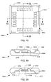
- FIG. 18 is a top view of a semiconductor package with upper and lower terminal pads on opposing sides of one of the semiconductor packages;
- FIG. 19 is a cross-sectional view of the structure of FIG. 18 taken along line 19 - 19 ;
- FIG. 20 is a cross-sectional view of the structure of FIG. 18 taken along line 20 - 20 ;
- FIG. 21 is a top view of stacked semiconductor packages with upper and lower terminal leads on opposing sides of the lower semiconductor package
- FIG. 22 is a cross-sectional view of the structure of FIG. 21 taken along line 22 - 22 ;
- FIG. 23 is a cross-sectional view of the structure of FIG. 21 taken along line 23 - 23 ;
- FIG. 24 is a top view of a semiconductor package with lower J-bent leads on opposing sides of the semiconductor package and a wrap around die pad;
- FIG. 25 is a cross-sectional view of the structure of FIG. 24 taken along line 25 - 25 ;
- FIG. 26 is a cross-sectional view of the structure of FIG. 24 taken along line 26 - 26 ;
- FIG. 27 is a side view of stacked semiconductor packages with lower gull-wing leads, lower J-bent leads, and a wrap around die pad;
- FIG. 28 is a cross-sectional view of the structure of FIG. 27 taken along line 28 - 28 ;
- FIG. 29 is a flow chart of a method for stacking semiconductor packages in accordance with the present invention.
- horizontal as used herein is defined as a plane parallel to the conventional plane or surface of the semiconductor package, regardless of its orientation.
- vertical refers to a direction perpendicular to the horizontal as just defined. Terms, such as “on”, “above”, “below”, “bottom”, “top”, “upper”, “side” (as in “sidewall”), “higher”, “lower”, “over”, and “under”, are defined with respect to the horizontal plane.
- FIG. 1 therein is shown a top view of a semiconductor package 110 with a number of upper gull wing leads 112 and a number of lower gull-wing leads 114 on opposing sides of the semiconductor package 110 .
- the number of upper gull-wing leads 112 has a number of widened lead tips 116 .
- the number of widened lead tips 116 is pre-plated to facilitate connection of the number of upper gull-wing leads 112 as described below.
- the semiconductor package 110 includes an encapsulant 118 from which the upper gull-wing leads 112 and the number of lower gull-wing leads 114 extend.
- the encapsulant 118 typically is a plastic, epoxy resin, or other suitable molding compound.
- the encapsulant typically has a sloped perimeter 111 to facilitate removal of the semiconductor package 110 from a mold.
- the semiconductor package 110 includes a die pad 200 .
- An integrated circuit chip, or a die 202 is attached to the die pad 200 using a suitable adhesive layer 204 , such as a conductive adhesive paste or tape.
- the die 202 is wire bonded to the die pad 200 using a first number of bonding wires 206 , such as a plurality of fine, conductive wires, typically gold (Au) or aluminum (Al).
- the die 202 also is wire bonded to the upper gull-wing leads 112 using a second number of bonding wires 208 .
- the encapsulant 118 encloses the die 202 and the bonding wires 206 and 208 .
- the upper gull-wing leads 112 extend outwardly from the encapsulant 118 to allow electrical connection of the die 202 to a second semiconductor package as explained below.
- FIG. 3 therein is shown a cross-sectional view of the structure of FIG. 1 taken along line 3 - 3 .
- the die 202 is wire bonded to the lower gull-wing leads 114 using a third number of bonding wires 300 .
- the third number of bonding wires 300 is connected using any suitable wire bonding process.
- the lower gull-wing leads 114 are used for attachment to another semiconductor package or printed circuit board (PCB).
- PCB printed circuit board
- FIG. 4 therein is shown a top view of a stack of semiconductor packages 400 with a number of upper gull-wing leads 112 and a number of lower gull-wing leads 114 on the semiconductor package 110 .
- the semiconductor package 110 shown in FIGS. 1-3 is referred to as the bottom semiconductor package 110 shown in FIG. 4 .
- a second semiconductor package 402 is attached to the bottom semiconductor package 110 .
- the second semiconductor package 402 includes a third number of lower gull-wing leads 404 extending outwardly from a second encapsulant 406 .
- the third number of lower gull-wing leads 404 is connected to the number of upper gull-wing leads 112 at the number of widened terminal pads 116 using conventional bonding techniques known in the semiconductor industry.
- FIG. 5 therein is shown a cross-sectional view of the structure of FIG. 4 taken along line 5 - 5 .
- the second semiconductor package 402 is connected to the bottom semiconductor package 110 .
- the third number of upper gull-wing leads 404 is soldered to the number of upper gull-wing leads 112 at the widened lead tip 116 using a solder 500 , such as a eutectic solder, a high lead solder, a lead-free solder, a pre-form solder, an electrically and thermally conductive paste adhesive, an electrically and thermally conductive film adhesive, and combinations thereof.
- a solder 500 such as a eutectic solder, a high lead solder, a lead-free solder, a pre-form solder, an electrically and thermally conductive paste adhesive, an electrically and thermally conductive film adhesive, and combinations thereof.
- suitable bonding techniques such as compression bonding or ultrasonic bonding, for example, also may be used to connect the third number of upper gull-wing leads 404 to the number of upper gull-wing leads 112 to form the stack of semiconductor packages 400 .
- the second semiconductor package 402 is attached to the bottom semiconductor package 110 at board assembly to avoid possible damage to the numbers of leads that may occur while picking and placing the stack of semiconductor packages 400 as a unit.
- the second semiconductor package 402 may also include a number of upper gull-wing leads for stacking another semiconductor package onto the second semiconductor package 402 .
- FIG. 6 therein is shown a top view of a semiconductor package 600 having a number of lower gull-wing leads 602 and a number of upper J-bent leads 604 on opposing sides of the semiconductor package 600 .
- the number of upper J-bent leads 604 have a widened lead tip 606 .
- the widened lead tip 606 is pre-plated, for example with tin-lead solder, lead-free solder, nickel-palladium-gold alloy, or a combination thereof, to facilitate connection of the number of upper J-bent leads 604 as described below.
- the semiconductor package 600 includes an encapsulant 608 from which the number of upper J-bent leads 604 and the number of lower gull-wing leads 602 extends.
- the encapsulant 608 typically is a plastic, epoxy resin, or other suitable molding compound.
- the encapsulant typically has a sloped perimeter 610 to facilitate removal of the semiconductor package 600 from a mold.
- the semiconductor package 600 includes a die pad 700 .
- An integrated circuit chip, or a die 702 is attached to the die pad 700 using a suitable adhesive layer 704 , such as a conductive adhesive paste or tape.
- the die 702 is wire bonded to the die pad 700 using a first number of bonding wires 706 , such as a plurality of fine, conductive wires, typically gold (Au) or aluminum (Al).
- the die 702 also is wire bonded to the number of upper J-bent leads 604 using a second number of bonding wires 708 .
- the encapsulant 608 encloses the die 702 and the bonding wires 706 and 708 .
- the upper J-bent leads 604 extend outwardly from the encapsulant 608 to allow electrical connection of the die 702 to a second semiconductor package as explained below.
- FIG. 8 therein is shown a cross-sectional view of the structure of FIG. 6 taken along line 8 - 8 .
- the die 702 is wire bonded to the number of lower gull-wing leads 602 using a third number of bonding wires 800 .
- the third number of bonding wires 800 is connected using any suitable wire bonding process.
- the number of lower gull-wing leads 602 is used for attachment to another semiconductor package or printed circuit board (PCB).
- PCB printed circuit board
- FIG. 9 therein is shown a top view of a stack of semiconductor packages 900 with the number of J-bent leads 604 on the bottom semiconductor package 600 .
- the semiconductor package 600 shown in FIGS. 6-8 is the bottom semiconductor package 600 shown in FIG. 9 .
- a second semiconductor package 902 is attached to the number of upper J-bent leads 604 of the bottom semiconductor package 600 at the widened lead tips 606 .
- the second semiconductor package 902 is connected to the bottom semiconductor package 600 .
- the second semiconductor package is a bottom leaded semiconductor package having a number of bottom leads 1100 .
- the number of bottom leads 1000 is soldered to the number of upper J-bent leads 604 at the widened lead tip 606 using a solder, such as a eutectic solder, a high lead solder, a lead-free solder, a pre-form solder, an electrically and thermally conductive paste adhesive, an electrically and thermally conductive film adhesive, and combinations thereof.
- suitable bonding techniques such as compression bonding or ultrasonic bonding, for example, also may be used to connect the number of bottom leads 1100 to the number of upper J-bent leads 604 to form the stack of semiconductor packages 900 .
- the second semiconductor package 902 is attached to the bottom semiconductor package 600 at board assembly to avoid possible damage to the numbers of leads that may occur while picking and placing the stacked semiconductor packages 900 as a unit.
- the second semiconductor package 902 may also include a number of upper gull-wing leads for stacking another semiconductor package onto the second semiconductor package 902 .
- FIG. 11 therein is shown a cross-sectional view of the structure of FIG. 9 taken along line 11 - 11 .
- the number of bottom leads 1100 is connected to the number of upper J-bent leads 604 to connect the second semiconductor package 902 to the bottom semiconductor package 600 .
- FIG. 12 therein is shown a top view of a semiconductor package 1200 with a number of lower J-bent leads 1202 and a number of upper J-bent leads 1204 on opposing sides of the semiconductor package 1200 .
- the number of upper J-bent leads 1204 has a number of widened lead tips 1206 .
- the number of widened lead tips 1206 is pre-plated to facilitate connection of the number of upper J-bent leads 1204 as described below.
- the semiconductor package 1200 includes an encapsulant 1208 from which the number of lower J-bent leads 1202 and the number of upper J-bent leads 1204 extend.
- the encapsulant 1208 typically is a plastic, epoxy resin, or other suitable molding compound.
- the encapsulant typically has a sloped perimeter 1210 to facilitate removal of the semiconductor package 1200 from a mold.
- the semiconductor package 1200 includes a die pad 1100 .
- An integrated circuit chip, or a die 1102 is attached to the die pad 1100 using a suitable adhesive layer 1104 , such as a conductive adhesive paste or tape.
- the die 1102 is wire bonded to the die pad 1100 using a first number of bonding wires 1106 , such as a plurality of fine, conductive wires, typically gold (Au) or aluminum (Al).
- the die 1302 also is wire bonded to the number of upper J-bent leads 1304 using a second number of bonding wires 1308 .
- the encapsulant 1208 encloses the die 1302 and the bonding wires 1306 and 1308 .
- the upper J-bent leads 1204 extend outwardly from the encapsulant 1208 to allow electrical connection of the die 1102 to a second semiconductor package as explained below.
- FIG. 11 therein is shown a cross-sectional view of the structure of FIG. 12 taken along line 14 - 14 .
- the die 1302 is wire bonded to the number of lower J-bent leads 1302 using a third number of bonding wires 1400 .
- the third number of bonding wires 1400 is connected using any suitable wire bonding process.
- the lower J-bent leads 1102 are used for attachment to another semiconductor package or printed circuit board (PCB).
- FIG. 11 therein is shown a top view of a stack of semiconductor packages 1500 with the number of lower J-bent leads 1202 and the number of upper J-bent leads 1204 on opposing sides of one of the bottom semiconductor package 1200 .
- the semiconductor package 1200 shown in FIGS. 12-14 is the bottom semiconductor package 1200 shown in FIG. 15 .
- a second semiconductor package 1502 is attached to the number of upper J-bent leads 1204 of the bottom semiconductor package 1200 at the number of widened lead tips 1206 .
- the second semiconductor package 1102 is connected to the bottom semiconductor package 1200 .
- the second semiconductor package 1502 is a bottom leaded semiconductor package having a number of bottom leads 1100 .
- the number of bottom leads 1600 is soldered to the number of upper J-bent leads 1204 at the widened lead tip 1106 using a solder, such as a eutectic solder, a high lead solder, a lead-free solder, a pre-form solder, an electrically and thermally conductive paste adhesive, an electrically and thermally conductive film adhesive, and combinations thereof.
- suitable bonding techniques such as compression bonding or ultrasonic bonding, for example, also may be used to connect the number of bottom leads 1100 to the number of upper J-bent leads 1204 to form the stack of semiconductor packages 1500 .
- the second semiconductor package 1502 is attached to the bottom semiconductor package 1200 at board assembly to avoid possible damage to the numbers of leads that may occur while picking and placing the stacked semiconductor packages 1500 as a unit.
- the second semiconductor package 1102 may also include a number of upper leads for stacking another semiconductor package onto the second semiconductor package 1502 .
- FIG. 11 therein is shown a cross-sectional view of the structure of FIG. 11 taken along line 11 - 11 .
- the number of bottom leads 1100 is connected to the number of upper J-bent leads 1104 to connect the second semiconductor package 1102 to the bottom semiconductor package 1200 .
- FIG. 11 therein is shown a top view of a semiconductor package 1100 with a number of lower terminal pads 1102 and a number of upper terminal pads 1104 on opposing sides of the semiconductor package 1100 .
- the semiconductor package 1100 includes an encapsulant 1108 from which the number of lower terminal pads 1102 and the number of upper terminal pads 1104 are exposed.
- the encapsulant 1208 typically is a plastic, epoxy resin, or other suitable molding compound.
- the encapsulant typically has a sloped perimeter 1111 to facilitate removal of the semiconductor package 1100 from a mold.
- the semiconductor package 1100 includes a die pad 1100 .
- An integrated circuit chip, or a die 1102 is attached to the die pad 1100 using a suitable adhesive layer 1104 , such as a conductive adhesive paste or tape.
- the die 1102 is wire bonded to a number of upper gull-wing leads 1105 that terminate in the upper terminal pads 1104 using a number of bonding wires 1108 , such as a plurality of fine, conductive wires, typically gold (Au) or aluminum (Al).
- the encapsulant 1108 encloses the die 1102 and the number of bonding wires 1108 .
- the number of upper gull-wing leads 1105 is embedded in the encapsulant 1108 to expose a surface of the upper terminal pads 1104 to allow electrical connection of the die 1102 to a second semiconductor package as explained below.
- FIG. 20 therein is shown a cross-sectional view of the structure of FIG. 11 taken along line 20 - 20 .
- the die 1102 is wire bonded to a number of lower gull-wing leads 2000 that terminate in the number of lower terminal pads 1102 using a third number of bonding wires 2002 .
- the third number of bonding wires 2002 is connected using any suitable wire bonding process.
- the number of lower gull-wing leads 2000 is embedded in the encapsulant 1108 to expose a surface of the lower terminal pads 1102 to allow electrical connection of the die 1102 to another semiconductor package or printed circuit board (PCB).
- PCB printed circuit board
- FIG. 21 therein is shown a top view of a stack of semiconductor packages 2110 with the number of lower terminal pads 1102 and the number of upper terminal pads 1104 on opposing sides of the bottom semiconductor package 1100 .
- the semiconductor package 1100 shown in FIGS. 11-20 is the bottom semiconductor package 1100 shown in FIG. 20 .
- a second semiconductor package 2112 is attached to the upper terminal pads 1104 of the bottom semiconductor package 1100 .
- the second semiconductor package 2102 is connected to the bottom semiconductor package 1800 .
- the second semiconductor package 2102 is a bottom leaded semiconductor package having a number of bottom leads 2200 .
- the number of bottom leads 2200 is soldered to the number of upper terminal pads 1104 using a solder, such as a eutectic solder, a high lead solder, a lead-free solder, a pre-form solder, an electrically and thermally conductive paste adhesive, an electrically and thermally conductive film adhesive, and combinations thereof.
- suitable bonding techniques such as compression bonding or ultrasonic bonding, for example, also may be used to connect the number of bottom leads 2200 to the number of upper terminal pads 1804 to form the stack of semiconductor packages 2100 .
- the second semiconductor package 2102 is attached to the bottom semiconductor package 1100 at board assembly to avoid possible damage to the numbers of leads that may occur while picking and placing the stacked semiconductor packages 2100 as a unit.
- the second semiconductor package 2112 may also include a number of upper leads or terminal pads for stacking another semiconductor package onto the second semiconductor package 2102 .
- FIG. 23 therein is shown a cross-sectional view of the structure of FIG. 21 taken along line 23 - 23 .
- the number of bottom leads 2200 is connected to the number of upper terminal pads 1104 shown in FIG. 22 to connect the second semiconductor package 2102 to the bottom semiconductor package 1800 .
- the number of lower terminal pads 1102 is exposed through the encapsulant for connection of the bottom semiconductor package 1100 to another semiconductor package or a PCB.
- FIG. 24 therein is shown a top view of a semiconductor package 2400 with a number of lower J-bent leads 2402 on opposing sides of the semiconductor package 2400 and a wrap around die pad 2404 having an upper surface 2406 .
- the wrap around die pad 2404 extends outwardly from opposing sides of an encapsulant 2408 and is positioned over the encapsulant 2408 .
- the encapsulant 2408 typically is a plastic, epoxy resin, or other suitable molding compound.
- the encapsulant 2408 typically has a sloped perimeter 2411 to facilitate removal of the semiconductor package 2400 from a mold.
- the semiconductor package 2400 includes a wrap around die pad 2500 .
- An integrated circuit chip, or a die 2502 is attached to the wrap around die pad 2500 using a suitable adhesive layer 2504 , such as a conductive adhesive paste or tape.
- the die 2502 is wire bonded to the wrap around die pad 2500 using a number of bonding wires 2508 , such as a plurality of fine, conductive wires, typically gold (Au) or aluminum (Al).
- the encapsulant 2408 encloses the die 2502 and the number of bonding wires 2508 and exposes a lower surface of the wrap around die pad 2500 .
- the wrap around die pad 2500 extends outwardly through the encapsulant 2408 and wraps around the top of the encapsulant 2408 to form the upper surface 2406 of the wrap around die pad 2500 to allow electrical connection of the die 2502 to a second semiconductor package as explained below.
- FIG. 26 therein is shown a cross-sectional view of the structure of FIG. 24 taken along line 26 - 26 .
- the die 2502 is wire bonded to a number of lower J-bent leads 2600 using a third number of bonding wires 2602 .
- the third number of bonding wires 2602 is connected using any suitable wire bonding process.
- the number of lower J-bent leads 2600 extends through the encapsulant 2408 to allow electrical connection of the die 2502 to another semiconductor package or printed circuit board (PCB). It will be apparent to those skilled in the art upon a reading of this description that the number of lower J-bent leads 2600 may be gull-wing leads as described above.
- FIG. 27 is a cross-sectional view of a stack of semiconductor packages 2700 with a bottom semiconductor package 2702 having a number of lower gull-wing leads 2704 and a first wrap around die pad 2706 and a second semiconductor package 2708 having a number of lower J-bent leads 2710 and a second wrap around die pad 2712 .
- the second semiconductor package 2708 is connected to the bottom semiconductor package 2702 .
- the number of lower J-bent leads 2710 is soldered to the number of lower gull-wing leads 2704 using a solder 2714 , such as a eutectic solder, a high lead solder, a lead-free solder, a pre-form solder, an electrically and thermally conductive paste adhesive, an electrically and thermally conductive film adhesive, and combinations thereof.
- suitable bonding techniques such as compression bonding or ultrasonic bonding, for example, also may be used to connect the number of lower J-bent leads 2710 to the number of lower gull-wing leads 2704 to form the stack of semiconductor packages 2700 .
- the second semiconductor package 2708 is attached to the bottom semiconductor package 2702 at board assembly to avoid possible damage to the numbers of leads that may occur while picking and placing the stack of semiconductor packages 2700 as a unit.
- the second wrap around die pad 2712 is attached to the first wrap around die pad 2706 using an adhesive layer 2711 , such as a conductive adhesive paste or adhesive tape.
- the second semiconductor package 2708 may also have another semiconductor package stacked on top of the second semiconductor package 2708 to form a stack of more than two semiconductor packages.
- FIG. 28 therein is shown a side view of the structure of FIG. 27 taken along line 28 - 28 .
- the first wrap around die pad 2706 is connected to the second wrap around die pad 2712 to connect the second semiconductor package 2708 to the bottom semiconductor package 2702 using the adhesive layer 2711 .
- the method 2900 includes providing a first semiconductor package having a first plurality of lower leads and a first plurality of upper leads in a block 2902 ; providing a second semiconductor package having a second plurality of lower leads in a block 2904 ; and attaching the second plurality of lower leads to the first plurality of upper leads in a block 2906 .
Abstract
Description
Claims (20)
Priority Applications (2)
| Application Number | Priority Date | Filing Date | Title |
|---|---|---|---|
| US10/906,697 US7242091B2 (en) | 2005-03-02 | 2005-03-02 | Stacked semiconductor packages and method therefor |
| US11/760,712 US7622800B2 (en) | 2005-03-02 | 2007-06-08 | Stacked semiconductor packages and method therefor |
Applications Claiming Priority (1)
| Application Number | Priority Date | Filing Date | Title |
|---|---|---|---|
| US10/906,697 US7242091B2 (en) | 2005-03-02 | 2005-03-02 | Stacked semiconductor packages and method therefor |
Related Child Applications (1)
| Application Number | Title | Priority Date | Filing Date |
|---|---|---|---|
| US11/760,712 Continuation US7622800B2 (en) | 2005-03-02 | 2007-06-08 | Stacked semiconductor packages and method therefor |
Publications (2)
| Publication Number | Publication Date |
|---|---|
| US20060197205A1 US20060197205A1 (en) | 2006-09-07 |
| US7242091B2 true US7242091B2 (en) | 2007-07-10 |
Family
ID=36943352
Family Applications (2)
| Application Number | Title | Priority Date | Filing Date |
|---|---|---|---|
| US10/906,697 Active 2025-08-05 US7242091B2 (en) | 2005-03-02 | 2005-03-02 | Stacked semiconductor packages and method therefor |
| US11/760,712 Active 2025-10-10 US7622800B2 (en) | 2005-03-02 | 2007-06-08 | Stacked semiconductor packages and method therefor |
Family Applications After (1)
| Application Number | Title | Priority Date | Filing Date |
|---|---|---|---|
| US11/760,712 Active 2025-10-10 US7622800B2 (en) | 2005-03-02 | 2007-06-08 | Stacked semiconductor packages and method therefor |
Country Status (1)
| Country | Link |
|---|---|
| US (2) | US7242091B2 (en) |
Cited By (2)
| Publication number | Priority date | Publication date | Assignee | Title |
|---|---|---|---|---|
| US20070290335A1 (en) * | 2006-04-28 | 2007-12-20 | Kabushiki Kaisha Toshiba | High-frequency semiconductor device |
| US20090069073A1 (en) * | 2007-09-12 | 2009-03-12 | Igt | Gaming device and method providing a plurality of plays of a background game resulting in a single award for the player |
Families Citing this family (10)
| Publication number | Priority date | Publication date | Assignee | Title |
|---|---|---|---|---|
| DE102005046134B4 (en) * | 2005-09-27 | 2014-05-15 | Qimonda Ag | Method for information forwarding with electronic components and correspondingly designed module |
| US7868471B2 (en) * | 2007-09-13 | 2011-01-11 | Stats Chippac Ltd. | Integrated circuit package-in-package system with leads |
| US20090091009A1 (en) * | 2007-10-03 | 2009-04-09 | Corisis David J | Stackable integrated circuit package |
| US8310098B2 (en) | 2011-05-16 | 2012-11-13 | Unigen Corporation | Switchable capacitor arrays for preventing power interruptions and extending backup power life |
| US9601417B2 (en) * | 2011-07-20 | 2017-03-21 | Unigen Corporation | “L” shaped lead integrated circuit package |
| KR20130046487A (en) * | 2011-10-28 | 2013-05-08 | 삼성전기주식회사 | Semiconductor package |
| DE102012204296B4 (en) * | 2012-03-19 | 2023-02-09 | Robert Bosch Gmbh | electronic assembly |
| DE102014107729B4 (en) * | 2014-06-02 | 2022-05-12 | Infineon Technologies Ag | Three-dimensional stack of a leaded package and an electronic element and method of making such a stack |
| CN106601694B (en) * | 2015-10-16 | 2020-09-15 | 台达电子工业股份有限公司 | Stack structure and manufacturing method thereof |
| JP7215344B2 (en) * | 2019-06-11 | 2023-01-31 | 株式会社デンソー | semiconductor equipment |
Citations (11)
| Publication number | Priority date | Publication date | Assignee | Title |
|---|---|---|---|---|
| US5978227A (en) * | 1993-03-29 | 1999-11-02 | Staktek Corporation | Integrated circuit packages having an externally mounted lead frame having bifurcated distal lead ends |
| US6459148B1 (en) * | 2000-11-13 | 2002-10-01 | Walsin Advanced Electronics Ltd | QFN semiconductor package |
| US6509639B1 (en) | 2001-07-27 | 2003-01-21 | Charles W. C. Lin | Three-dimensional stacked semiconductor package |
| US6512290B2 (en) | 1997-12-31 | 2003-01-28 | Micron Technology, Inc. | Vertically mountable and alignable semiconductor device, assembly, and methods |
| US6656767B1 (en) | 1998-03-09 | 2003-12-02 | Micron Technology, Inc. | Method of forming a stack of packaged memory dice |
| US6753207B2 (en) | 2000-01-04 | 2004-06-22 | Hyundai Electronics Industries Co., Ltd. | Stacked semiconductor package and fabricating method thereof |
| US6765287B1 (en) | 2001-07-27 | 2004-07-20 | Charles W. C. Lin | Three-dimensional stacked semiconductor package |
| US6773959B2 (en) | 2002-03-01 | 2004-08-10 | Sampson Taiwan Ltd. | Method for stacking semiconductor package units and stacked package |
| US6773955B2 (en) | 1998-08-21 | 2004-08-10 | Micron Technology, Inc. | Low profile multi-IC chip package connector |
| US6806120B2 (en) | 2001-03-27 | 2004-10-19 | Staktek Group, L.P. | Contact member stacking system and method |
| US6828665B2 (en) | 2002-10-18 | 2004-12-07 | Siliconware Precision Industries Co., Ltd. | Module device of stacked semiconductor packages and method for fabricating the same |
Family Cites Families (2)
| Publication number | Priority date | Publication date | Assignee | Title |
|---|---|---|---|---|
| KR970010678B1 (en) * | 1994-03-30 | 1997-06-30 | 엘지반도체 주식회사 | Lead frame and the package thereof |
| KR100421774B1 (en) * | 1999-12-16 | 2004-03-10 | 앰코 테크놀로지 코리아 주식회사 | semiconductor package and its manufacturing method |
-
2005
- 2005-03-02 US US10/906,697 patent/US7242091B2/en active Active
-
2007
- 2007-06-08 US US11/760,712 patent/US7622800B2/en active Active
Patent Citations (13)
| Publication number | Priority date | Publication date | Assignee | Title |
|---|---|---|---|---|
| US5978227A (en) * | 1993-03-29 | 1999-11-02 | Staktek Corporation | Integrated circuit packages having an externally mounted lead frame having bifurcated distal lead ends |
| US6531764B2 (en) | 1997-12-31 | 2003-03-11 | Micron Technology, Inc. | Vertically mountable semiconductor device, assembly, and methods |
| US6512290B2 (en) | 1997-12-31 | 2003-01-28 | Micron Technology, Inc. | Vertically mountable and alignable semiconductor device, assembly, and methods |
| US6656767B1 (en) | 1998-03-09 | 2003-12-02 | Micron Technology, Inc. | Method of forming a stack of packaged memory dice |
| US6773955B2 (en) | 1998-08-21 | 2004-08-10 | Micron Technology, Inc. | Low profile multi-IC chip package connector |
| US6753207B2 (en) | 2000-01-04 | 2004-06-22 | Hyundai Electronics Industries Co., Ltd. | Stacked semiconductor package and fabricating method thereof |
| US6459148B1 (en) * | 2000-11-13 | 2002-10-01 | Walsin Advanced Electronics Ltd | QFN semiconductor package |
| US6806120B2 (en) | 2001-03-27 | 2004-10-19 | Staktek Group, L.P. | Contact member stacking system and method |
| US6509639B1 (en) | 2001-07-27 | 2003-01-21 | Charles W. C. Lin | Three-dimensional stacked semiconductor package |
| US6765287B1 (en) | 2001-07-27 | 2004-07-20 | Charles W. C. Lin | Three-dimensional stacked semiconductor package |
| US6794741B1 (en) | 2001-07-27 | 2004-09-21 | Bridge Semiconductor Corporation | Three-dimensional stacked semiconductor package with pillars in pillar cavities |
| US6773959B2 (en) | 2002-03-01 | 2004-08-10 | Sampson Taiwan Ltd. | Method for stacking semiconductor package units and stacked package |
| US6828665B2 (en) | 2002-10-18 | 2004-12-07 | Siliconware Precision Industries Co., Ltd. | Module device of stacked semiconductor packages and method for fabricating the same |
Cited By (5)
| Publication number | Priority date | Publication date | Assignee | Title |
|---|---|---|---|---|
| US20070290335A1 (en) * | 2006-04-28 | 2007-12-20 | Kabushiki Kaisha Toshiba | High-frequency semiconductor device |
| US7667322B2 (en) * | 2006-04-28 | 2010-02-23 | Kabushiki Kaisha Toshiba | High-frequency semiconductor device |
| US20100102443A1 (en) * | 2006-04-28 | 2010-04-29 | Kabushiki Kaisha Toshiba | High-frequency semiconductor device |
| US7994637B2 (en) | 2006-04-28 | 2011-08-09 | Kabushiki Kaisha Toshiba | High-frequency semiconductor device |
| US20090069073A1 (en) * | 2007-09-12 | 2009-03-12 | Igt | Gaming device and method providing a plurality of plays of a background game resulting in a single award for the player |
Also Published As
| Publication number | Publication date |
|---|---|
| US7622800B2 (en) | 2009-11-24 |
| US20060197205A1 (en) | 2006-09-07 |
| US20070228545A1 (en) | 2007-10-04 |
Similar Documents
| Publication | Publication Date | Title |
|---|---|---|
| US7622800B2 (en) | Stacked semiconductor packages and method therefor | |
| US7619314B2 (en) | Integrated circuit package system including die stacking | |
| US7309913B2 (en) | Stacked semiconductor packages | |
| US8710675B2 (en) | Integrated circuit package system with bonding lands | |
| US7915716B2 (en) | Integrated circuit package system with leadframe array | |
| US6080264A (en) | Combination of semiconductor interconnect | |
| US7719094B2 (en) | Semiconductor package and manufacturing method thereof | |
| US8183089B2 (en) | Method for manufacturing package system incorporating flip-chip assembly | |
| US20020158318A1 (en) | Multi-chip module | |
| US8786063B2 (en) | Integrated circuit packaging system with leads and transposer and method of manufacture thereof | |
| US8395251B2 (en) | Integrated circuit package to package stacking system | |
| US7977780B2 (en) | Multi-layer package-on-package system | |
| US9093391B2 (en) | Integrated circuit packaging system with fan-in package and method of manufacture thereof | |
| KR101590540B1 (en) | Integrated circuit packaging system with base structure device | |
| US20040241908A1 (en) | Semiconductor package with semiconductor chips stacked therein and method of making the package | |
| US8203214B2 (en) | Integrated circuit package in package system with adhesiveless package attach | |
| SG173394A1 (en) | Integrated circuit leadframe and fabrication method therefor | |
| KR20040075245A (en) | Stacked semiconductor package and fabricating method the same | |
| US20060284298A1 (en) | Chip stack package having same length bonding leads | |
| US6791166B1 (en) | Stackable lead frame package using exposed internal lead traces | |
| US6849952B2 (en) | Semiconductor device and its manufacturing method | |
| US20080308933A1 (en) | Integrated circuit package system with different connection structures | |
| US7804166B2 (en) | Integrated circuit package system with stacking module | |
| KR100708050B1 (en) | semiconductor package | |
| KR20080058013A (en) | Multi-chip package and method of manufacturing the same |
Legal Events
| Date | Code | Title | Description |
|---|---|---|---|
| AS | Assignment |
Owner name: STATS CHIPPAC LTD., SINGAPORE Free format text: ASSIGNMENT OF ASSIGNORS INTEREST;ASSIGNORS:RAMAKRISHNA, KAMBHAMPATI;SHIM, IL KWON;CHOW, SENG GUAN;REEL/FRAME:015721/0070 Effective date: 20050217 |
|
| AS | Assignment |
Owner name: STATS CHIPPAC LTD., SINGAPORE Free format text: ASSIGNMENT OF ASSIGNORS INTEREST;ASSIGNORS:RAMAKRISHNA, KAMBHAMPATI;SHIM, IL KWON;CHOW, SENG GUAN;REEL/FRAME:015804/0794 Effective date: 20050217 |
|
| STCF | Information on status: patent grant |
Free format text: PATENTED CASE |
|
| CC | Certificate of correction | ||
| FPAY | Fee payment |
Year of fee payment: 4 |
|
| FPAY | Fee payment |
Year of fee payment: 8 |
|
| AS | Assignment |
Owner name: CITICORP INTERNATIONAL LIMITED, AS COMMON SECURITY AGENT, HONG KONG Free format text: SECURITY INTEREST;ASSIGNORS:STATS CHIPPAC, INC.;STATS CHIPPAC LTD.;REEL/FRAME:036288/0748 Effective date: 20150806 Owner name: CITICORP INTERNATIONAL LIMITED, AS COMMON SECURITY Free format text: SECURITY INTEREST;ASSIGNORS:STATS CHIPPAC, INC.;STATS CHIPPAC LTD.;REEL/FRAME:036288/0748 Effective date: 20150806 |
|
| AS | Assignment |
Owner name: STATS CHIPPAC PTE. LTE., SINGAPORE Free format text: CHANGE OF NAME;ASSIGNOR:STATS CHIPPAC LTD.;REEL/FRAME:038378/0343 Effective date: 20160329 |
|
| MAFP | Maintenance fee payment |
Free format text: PAYMENT OF MAINTENANCE FEE, 12TH YEAR, LARGE ENTITY (ORIGINAL EVENT CODE: M1553); ENTITY STATUS OF PATENT OWNER: LARGE ENTITY Year of fee payment: 12 |
|
| AS | Assignment |
Owner name: STATS CHIPPAC PTE. LTD. FORMERLY KNOWN AS STATS CHIPPAC LTD., SINGAPORE Free format text: RELEASE BY SECURED PARTY;ASSIGNOR:CITICORP INTERNATIONAL LIMITED, AS COMMON SECURITY AGENT;REEL/FRAME:052938/0305 Effective date: 20190503 Owner name: STATS CHIPPAC, INC., CALIFORNIA Free format text: RELEASE BY SECURED PARTY;ASSIGNOR:CITICORP INTERNATIONAL LIMITED, AS COMMON SECURITY AGENT;REEL/FRAME:052938/0305 Effective date: 20190503 |