US7319829B2 - Transfer bias adjustment based on component life - Google Patents
Transfer bias adjustment based on component life Download PDFInfo
- Publication number
- US7319829B2 US7319829B2 US11/212,218 US21221805A US7319829B2 US 7319829 B2 US7319829 B2 US 7319829B2 US 21221805 A US21221805 A US 21221805A US 7319829 B2 US7319829 B2 US 7319829B2
- Authority
- US
- United States
- Prior art keywords
- component
- transfer
- age
- image forming
- resistance
- Prior art date
- Legal status (The legal status is an assumption and is not a legal conclusion. Google has not performed a legal analysis and makes no representation as to the accuracy of the status listed.)
- Active - Reinstated, expires
Links
- 238000012546 transfer Methods 0.000 title claims description 98
- 230000004044 response Effects 0.000 claims abstract description 11
- 238000000034 method Methods 0.000 claims description 29
- 239000011248 coating agent Substances 0.000 claims description 23
- 238000000576 coating method Methods 0.000 claims description 23
- 230000003247 decreasing effect Effects 0.000 claims 1
- 230000007613 environmental effect Effects 0.000 abstract description 7
- 230000008569 process Effects 0.000 description 13
- 230000008859 change Effects 0.000 description 10
- 238000012360 testing method Methods 0.000 description 5
- 238000013459 approach Methods 0.000 description 4
- 230000001419 dependent effect Effects 0.000 description 4
- 230000003287 optical effect Effects 0.000 description 4
- 239000002699 waste material Substances 0.000 description 4
- 238000004140 cleaning Methods 0.000 description 3
- 238000011161 development Methods 0.000 description 3
- 239000000463 material Substances 0.000 description 3
- 238000012545 processing Methods 0.000 description 3
- 238000004364 calculation method Methods 0.000 description 2
- 230000007423 decrease Effects 0.000 description 2
- 238000010586 diagram Methods 0.000 description 2
- 238000003384 imaging method Methods 0.000 description 2
- 239000002245 particle Substances 0.000 description 2
- 230000000737 periodic effect Effects 0.000 description 2
- XAGFODPZIPBFFR-UHFFFAOYSA-N aluminium Chemical compound [Al] XAGFODPZIPBFFR-UHFFFAOYSA-N 0.000 description 1
- 229910052782 aluminium Inorganic materials 0.000 description 1
- 230000015572 biosynthetic process Effects 0.000 description 1
- 238000006243 chemical reaction Methods 0.000 description 1
- 238000004590 computer program Methods 0.000 description 1
- 238000013461 design Methods 0.000 description 1
- 230000006866 deterioration Effects 0.000 description 1
- 239000006260 foam Substances 0.000 description 1
- 230000006870 function Effects 0.000 description 1
- 230000000977 initiatory effect Effects 0.000 description 1
- 238000009434 installation Methods 0.000 description 1
- 238000004519 manufacturing process Methods 0.000 description 1
- 230000007246 mechanism Effects 0.000 description 1
- 238000012986 modification Methods 0.000 description 1
- 230000004048 modification Effects 0.000 description 1
- 230000000644 propagated effect Effects 0.000 description 1
- 238000003860 storage Methods 0.000 description 1
- 239000000758 substrate Substances 0.000 description 1
- 230000007704 transition Effects 0.000 description 1
Images


Classifications
-
- G—PHYSICS
- G03—PHOTOGRAPHY; CINEMATOGRAPHY; ANALOGOUS TECHNIQUES USING WAVES OTHER THAN OPTICAL WAVES; ELECTROGRAPHY; HOLOGRAPHY
- G03G—ELECTROGRAPHY; ELECTROPHOTOGRAPHY; MAGNETOGRAPHY
- G03G15/00—Apparatus for electrographic processes using a charge pattern
- G03G15/14—Apparatus for electrographic processes using a charge pattern for transferring a pattern to a second base
- G03G15/16—Apparatus for electrographic processes using a charge pattern for transferring a pattern to a second base of a toner pattern, e.g. a powder pattern, e.g. magnetic transfer
- G03G15/1665—Apparatus for electrographic processes using a charge pattern for transferring a pattern to a second base of a toner pattern, e.g. a powder pattern, e.g. magnetic transfer by introducing the second base in the nip formed by the recording member and at least one transfer member, e.g. in combination with bias or heat
- G03G15/167—Apparatus for electrographic processes using a charge pattern for transferring a pattern to a second base of a toner pattern, e.g. a powder pattern, e.g. magnetic transfer by introducing the second base in the nip formed by the recording member and at least one transfer member, e.g. in combination with bias or heat at least one of the recording member or the transfer member being rotatable during the transfer
- G03G15/1675—Apparatus for electrographic processes using a charge pattern for transferring a pattern to a second base of a toner pattern, e.g. a powder pattern, e.g. magnetic transfer by introducing the second base in the nip formed by the recording member and at least one transfer member, e.g. in combination with bias or heat at least one of the recording member or the transfer member being rotatable during the transfer with means for controlling the bias applied in the transfer nip
-
- G—PHYSICS
- G03—PHOTOGRAPHY; CINEMATOGRAPHY; ANALOGOUS TECHNIQUES USING WAVES OTHER THAN OPTICAL WAVES; ELECTROGRAPHY; HOLOGRAPHY
- G03G—ELECTROGRAPHY; ELECTROPHOTOGRAPHY; MAGNETOGRAPHY
- G03G15/00—Apparatus for electrographic processes using a charge pattern
- G03G15/55—Self-diagnostics; Malfunction or lifetime display
- G03G15/553—Monitoring or warning means for exhaustion or lifetime end of consumables, e.g. indication of insufficient copy sheet quantity for a job
- G03G15/556—Monitoring or warning means for exhaustion or lifetime end of consumables, e.g. indication of insufficient copy sheet quantity for a job for toner consumption, e.g. pixel counting, toner coverage detection or toner density measurement
-
- G—PHYSICS
- G03—PHOTOGRAPHY; CINEMATOGRAPHY; ANALOGOUS TECHNIQUES USING WAVES OTHER THAN OPTICAL WAVES; ELECTROGRAPHY; HOLOGRAPHY
- G03G—ELECTROGRAPHY; ELECTROPHOTOGRAPHY; MAGNETOGRAPHY
- G03G2215/00—Apparatus for electrophotographic processes
- G03G2215/16—Transferring device, details
- G03G2215/1604—Main transfer electrode
- G03G2215/1614—Transfer roll
Definitions
- Certain image forming devices use an electrophotographic imaging process to develop toner images on a media sheet.
- the electrophotographic process uses electrostatic voltage differentials to promote the transfer of toner from component to component.
- a voltage vector may exist between a developer roll and a latent image on a photoconductive element. This voltage vector helps promote the transfer of toner from the developer roll to the latent image in a process that is sometimes called “developing the image.”
- a separate voltage vector may exist between the photoconductive element and a transfer member to promote the transfer of a developed image onto a substrate. In each instance, the toner transfer occurs in part because the toner itself is charged and is attracted to surfaces having an opposite charge or a lower potential.
- the effective transfer of toner within an image forming device is usually dependent on many variables, including environmental conditions such as temperature and humidity. For example, in some systems there is an inverse relationship between humidity and transfer member resistance. Some image forming devices use dedicated temperature and humidity sensors to detect environmental conditions. These devices may alter operating parameters, such as the transfer bias applied to a transfer member, in response to the detected environmental conditions.
- image forming devices measure the voltage-current characteristics of a test signal propagated through components within the device. For example, some image forming devices transmit a signal through the interface between a transfer member and a photoconductive member. The resistance and capacitance characteristics over this interface change in relation to environmental conditions. Thus, the measured resistance/capacitance characteristics may be mapped in memory to environmental values or to actual operating parameters. Accordingly, device operating parameters may be set in response to the detected resistance/capacitance values.
- the mapped resistance/capacitance values may not account for component deterioration that occurs with wear and use. Over time, the correlation between the mapped resistance/capacitance values and suitable operating parameters may change. For example, the photoconductive layer capacitance increases with wear, thereby reducing the effective resistance. Thus, unless age and wear are accounted for, the device operating parameters that are set in response to detected resistance/capacitance values may produce degraded images.
- Embodiments of the present invention are directed to devices and methods to account for device age while setting operating parameters in an image forming device in response to periodic feedback loop checks.
- an image forming unit may comprise two or more components adapted to transfer a toner image therebetween.
- a sensing unit may detect a resistance/capacitance characteristic of a feedback loop comprising an interface between the components.
- the detected resistance/capacitance characteristic of the feedback loop may represent a detected voltage produced by passing a known current through the interface between the components.
- the detected resistance/capacitance characteristic of the feedback loop may represent a detected current produced by passing a known voltage through the interface between the components.
- a controller may adjust the detected resistance/capacitance characteristic in response to the age of one or more of the image forming unit components. The controller may also adjust the detected resistance/capacitance characteristic in response to a device throughput.
- the magnitude of the adjustment may be stored in memory as a lookup table comprising adjustment values corresponding to the age of one of the components.
- the magnitude of the adjustment also may be determined through linear or higher order equation calculations, with component age being an input variable.
- the age of a component may represent a number of revolutions experienced by a rotating member such as a photoconductive member.
- the age of a component may represent a number of pages printed by the image forming device.
- the age of a component may represent an elapsed time.
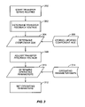
- FIG. 1 is a schematic view of an image forming device according to one embodiment of the present invention.
- FIG. 2 is a cross-sectional view of an image forming unit and associated power supply and transfer feedback circuit according to one embodiment of the present invention
- FIG. 3 is a flow diagram illustrating a process by which operating parameters may be adjusted in response to a detected device age according to one embodiment of the present invention.
- FIG. 4 is a representative lookup table showing transfer feedback adjustment values for various component ages and for various device throughputs according to one embodiment of the present invention.
- Embodiments disclosed herein are directed to devices and related methods to adjust component bias levels in an image forming device to compensate for component age and wear. These embodiments may be applicable in a device that uses an electrophotographic imaging process such as the representative image forming device 10 shown in FIG. 1 .
- the exemplary image forming device 10 comprises a main body 12 and a door assembly 13 .
- a media tray 98 with a pick mechanism 16 , and a multi-purpose feeder 32 are conduits for introducing media sheets into the device 10 .
- the media tray 98 is preferably removable for refilling, and located on a lower section of the device 10 .
- Media sheets are moved from the input and fed into a primary media path.
- One or more registration rollers 99 disposed along the media path aligns the print media and precisely controls its further movement along the media path.
- a media transport belt 20 forms a section of the media path for moving the media sheets past a plurality of image forming units 100 .
- Color printers typically include four image forming units 100 for printing with cyan, magenta, yellow, and black toner to produce a four-color image on the media sheet.
- An optical scanning device 22 forms a latent image on a photoconductive member 51 (not explicitly referenced in FIG. 1 , but see FIG. 2 ) within the image forming units 100 .
- the media sheet with loose toner is then moved through a fuser 24 to fix the toner to the media sheet.
- Exit rollers 26 rotate in a forward direction to move the media sheet to an output tray 28 , or rollers 26 rotate in a reverse direction to move the media sheet to a duplex path 30 .
- the duplex path 30 directs the inverted media sheet back through the image formation process for forming an image on a second side of the media sheet.
- the image forming units 100 are comprised of a developer unit 40 and a photoconductor (PC) unit 50 .
- the developer unit 40 comprises an exterior housing 43 that forms a reservoir 41 for holding a supply of toner 70 .
- One or more agitating members 42 are positioned within the reservoir 41 for agitating and moving the toner 70 towards a toner adding roll 44 and the developer member 45 .
- the developer unit 40 further comprises a doctor element 38 that controls the toner 70 layer formed on the developer member 45 .
- a cantilevered, flexible doctor blade as shown in FIG. 2 may be used.
- Other types of doctor elements 38 such as spring-loaded, ingot style doctor elements may be used.
- the developer unit 40 and PC unit 50 are structured so the developer member 45 is accessible for contact with the photoconductive member 51 at a nip 46 . Consequently, the developer member 45 is positioned to develop latent images formed on the photoconductive member 51 .
- the exemplary PC unit 50 comprises the photoconductive member 51 , a charge roller 52 , a cleaner blade 53 , and a waste toner auger 54 all disposed within a housing 62 that is separate from the developer unit housing 43 .
- the photoconductive member 51 is an aluminum hollow-core drum with a photoconductive coating 68 comprising one or more layers of light-sensitive organic photoconductive materials.
- the photoconductive member 51 is mounted protruding from the PC unit 50 to contact the developer member 45 at nip 46 .
- Charge roller 52 is electrified to a predetermined bias by a high voltage power supply (HVPS) 60 that is adjusted or turned on and off by a controller 64 .
- the charge roller 52 applies an electrical charge to the photoconductive coating 68 .
- HVPS high voltage power supply
- photoconductive coating 68 During image creation, selected portions of the photoconductive coating 68 are exposed to optical energy, such as laser light, through aperture 48 . Exposing areas of the photoconductive coating 68 in this manner creates a discharged latent image on the photoconductive member 51 . That is, the latent image is discharged to a lower charge level than areas of the photoconductive coating 68 that are not illuminated.
- optical energy such as laser light
- the developer member 45 (and hence, the toner 70 thereon) is charged to a bias level by the HVPS 60 that is advantageously set between the bias level of charge roller 52 and the discharged latent image.
- the developer member 45 is comprised of a resilient (e.g., foam or rubber) roller disposed around a conductive axial shaft.
- a resilient roller-type developer members 45 as are known in the art may be used.
- Charged toner 70 is carried by the developer member 45 to the latent image formed on the photoconductive coating 68 .
- the toner 70 is attracted to the latent image and repelled from the remaining, higher charged portions of the photoconductive coating 68 .
- the latent image is said to be developed.
- the developed image is subsequently transferred to a media sheet being carried past the photoconductive member 51 by media transport belt 20 .
- a transfer roller 34 is disposed behind the transport belt 20 in a position to impart a contact pressure at the transfer nip.
- the transfer roller 34 is advantageously charged, typically to a polarity that is opposite the charged toner 70 and charged photoconductive member 51 to promote the transfer of the developed image to the media sheet.
- the cleaner blade 53 contacts the outer surface of the photoconductive coating 68 to remove toner 70 that remains on the photoconductive member 51 following transfer of the developed image to a media sheet.
- the residual toner 70 is moved to a waste toner auger 54 .
- the auger 54 moves the waste toner 70 out of the photoconductor unit 50 and towards a waste toner container (not shown), which may be disposed of once full.
- the charge roller 52 , the photoconductive member 51 , the developer member 45 , the doctor element 38 and the toner adding roll 44 are all negatively biased.
- the transfer roller 34 may be positively biased to promote transfer of negatively charged toner 70 particles to a media sheet.
- an image forming unit 100 may implement polarities opposite from these.
- the HVPS 60 Periodically, such as between print jobs or at the start of a print job, the HVPS 60 , under the control of controller 64 , implements a transfer servo routine to determine a transfer feedback voltage that varies in relation to changing operating conditions.
- the printer controller 64 may adjust operating parameters (e.g., bias voltage applied to the transfer roller 34 or the fuser 24 shown in FIG. 1 ) based on the determined transfer feedback voltage to compensate for changes in operating conditions, including temperature and humidity.
- the transfer feedback voltage that produces a predetermined current through the transfer roller 34 is determined. More specifically, the HVPS 60 includes a sensing circuit 56 adapted to sense the voltage transmitted to the transfer roller 34 that produces a target current of 8 ⁇ A. This threshold circuit 56 produces a state change (i.e., low to high transition, otherwise referred to as a positive feedback) in a binary output signal that is sensed by the controller 64 when the transfer current equals or exceeds the target current of 8 ⁇ A. If the transfer current remains below the target current, the output of the sensing circuit 56 remains low.
- a state change i.e., low to high transition, otherwise referred to as a positive feedback
- the applied current travels through various components, including the transfer roller 34 , the media transport belt 20 , the photoconductive member 51 and ultimately to ground. Some of the applied current may also travel to ground via the cleaner blade 53 , charge roller 52 , and/or developer member 45 .
- the voltage that produces the target current is referred to as the “transfer feedback voltage.”
- the value of the transfer feedback voltage is transmitted to or otherwise determined by the controller 64 .
- operating parameters are mapped in memory 66 to different values of the transfer feedback voltage.
- the controller 64 reads the operating parameter for a measured transfer feedback voltage and, in turn, sets appropriate operating parameters for subsequent printing.
- FIG. 1 shows that there are four image forming units 100 in the representative image forming device.
- the process of determining the transfer feedback voltage may be performed for each transfer location in the image forming device 10 .
- the process is performed simultaneously at each image forming unit 100 .
- the process may be performed sequentially at each image forming unit 100 .
- the capacitance of the photoconductive coating 68 on the photoconductive member 51 is related to its thickness. A new photoconductive member 51 is coated to a specified thickness. However, during printing, the photoconductive coating 68 is worn by contact with other components, such as a cleaner blade 53 . As the photoconductive coating 68 thins due to wear, the capacitance of the junction between the photoconductive member 51 and other components in contact with the photoconductive coating 68 increases. For instance, the capacitance of the junction between the transfer roller 34 and the photoconductive member 51 increases as the photoconductive coating 68 thins. This increased capacitance causes the transfer feedback voltage to drop as the effective resistance of the feedback loop is reduced.
- This drop in resistance and transfer feedback voltage may be interpreted incorrectly by controller 64 as an increase in humidity.
- the printer controller 64 may tend to overcompensate for the erroneously low transfer feedback voltage.
- the change in capacitance of the photoconductive coating 68 on the photoconductive member 51 may become so great that the selected operating parameter falls outside a desired operating window. As a result, print quality likely degrades.
- an adjustment may be implemented based on knowledge that the rate of wear of the photoconductive coating 68 on the photoconductive member 51 is consistent and repeatable. Different approaches may be used to compensate for the changed capacitance of the photoconductive coating 68 .
- the capacitance of photoconductive coating 68 may correlate with a number of photoconductive member 51 revolutions. This age-dependent deviation may be represented by a function (linear or higher order) or a look up table. Then, during the transfer feedback process, the measured voltage may be adjusted based on the age of the photoconductive member 51 .
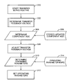
- the flow diagram illustrated in FIG. 3 shows one embodiment of a process by which this transfer feedback voltage adjustment may be implemented.
- the transfer servo routine begins.
- the process by which the transfer feedback voltage is determined as described above is executed.
- a sensing circuit 56 (see FIG. 2 ) is adapted to sense the voltage transmitted to the transfer roller 34 that produces a predetermined current.
- This transfer feedback voltage is determined in step 302 .
- the relevant component age is determined in step 304 .
- the age of a photoconductive member 51 is determined as an indication of the change in the photoconductive coating 68 on the photoconductive member 51 .
- the age of the photoconductive member 51 is maintained as a running, updated count representing the number of revolutions encountered by photoconductive member 51 since a new photoconductive member 51 was installed. Other age indicators may be used.
- the age of the photoconductive member 51 may be represented as a running clock measuring run time since a new photoconductor member 51 was installed.
- the age of the photoconductive member 51 is maintained as a running count representing the number of pages produced since a new photoconductor member 51 was installed.
- the controller 64 shown in FIG. 2
- the relevant component age may be used in step 308 to adjust the measured transfer feedback voltage.
- Different approaches may be used to adjust the measured transfer feedback voltage.
- a suitable adjustment may be executed as a mathematical calculation.
- V initial is the transfer feedback voltage measured in step 302
- V adjusted is the adjusted transfer feedback voltage determined in step 308
- the Age term is the component age read in step 304 and represents the age of the photoconductive member 51 in terms of the number of revolutions turned by the photoconductive member 51 since installation.
- the appropriate operating parameters for image forming device 10 may be determined (step 310 ) from stored data maps. These data maps may be predetermined and stored in memory 66 . For example, the operating parameter maps may be factory-set and stored during manufacturing. Alternatively, these operating parameter maps may be dependent upon periodic configuration routines that may include patch sensing or user-initiated print quality routines.
- the appropriate operating parameter maps are stored (step 314 ) for later access by controller 64 .
- the controller 64 may then set (step 312 ) these operating parameters accordingly.
- the controller may set the operating bias voltage for the transfer roller 34 .
- the controller 64 may set the operating bias voltage for the fuser 24 .
- the controller 64 may set the operating bias voltage for other image forming components shown in FIG. 2 , such as the charge roller 52 or developer member 45 .
- Equation (1) may be applicable for a certain print speed.
- the device throughput in pages per minute (PPM) may vary as well.
- Equation (1) may be applicable for a device throughput of about 20 PPM.
- a lower device throughput may correspond to a higher level of detail or a larger dots per inch (DPI) setting for the output images. Accordingly, a different transfer voltage adjustment may be necessary.
- Equation (2) below may be applicable with a device throughput of 10 PPM or 6 PPM.
- V adjusted V initial +K 2 ⁇ Age (2)
- the constant K2 associated with a lower device throughput may be larger than the constant K1.
- the value for the constant K1 associated with a device throughput of 20 PPM is between about 1.3-1.4 volts per 1000 revolutions.
- a corresponding value for the constant K2 associated with a device throughput of 10 PPM is between about 1.5-1.6 volts per 1000 revolutions.
- Different values for constants K1 and K2 may be appropriate depending on the component considered or other device applications.
- the wear rate may be dependent on the photoconductive material. It may also depend on the design and material used for the cleaning blade 53 . A stiffer cleaning blade 53 generally results in a faster wear rate.
- the amount of interference between the cleaning blade 53 and the photoconductive member 51 affects the wear rate—the greater the interference, the higher the wear rate.
- the wear rate may also be influenced by environment. These considerations may be relevant to the values used for constants K1 and K2.
- the amount by which the transfer feedback voltage is adjusted may be stored as a lookup table instead of equations, as presented above.
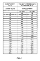
- An exemplary lookup table for the measured transfer feedback voltage is shown in FIG. 4 , which represents a table of adjustments that may be stored in memory 66 and accessed in step 308 to determine the relevant adjustment.
- the tabulated values shown in FIG. 4 may represent an adjustment to the transfer feedback voltage that is measured in step 302 of FIG. 3 .
- the values shown in FIG. 4 reflect a general increase in the amount of transfer feedback adjustment that is applied as component life increases. This increase may be applied to offset the expected change in capacitance of the photoconductive coating 68 on the photosensitive member 51 that comes with component age.
- different sets of adjustment values may be used for different device throughput speeds.
- the representative lookup table shown in FIG. 4 includes device age on one axis and device throughput speed on the other axis.
- the amount of transfer feedback voltage adjustment is determined by accessing the appropriate address for a given component age and throughput speed.
- test pulse may be carried out in other specific ways than those herein set forth without departing from the scope and essential characteristics of the invention.
- embodiments described above have contemplated transmitting a test pulse through a transfer roller 34 to determine the resistance/capacitance characteristics of image forming components that are involved in the transfer of toner.
- this type of test pulse may be transmitted through charge roller 52 or developer member 45 as shown in FIG. 2 .
- Different image forming devices 10 may also transmit a test pulse of a known voltage through the image forming units and determine the current produced by such a pulse.
- the resulting current may tend to increase with component wear.
- the capacitance increases and the effective resistance decreases, which results in larger current flow for a given voltage. Accordingly, the appropriate transfer bias adjustment may require a decrease in the measured current to account for age and wear.
- the representative image forming unit 100 shown in FIG. 2 includes a transport belt 20 that is disposed between a transfer roller 34 and a photoconductive member.
- the resistance/capacitance characteristics of this exemplary belt 20 may also change with age and wear.
- the resistance or capacitance of the belt 20 may increase with age.
- the measured transfer feedback voltage may require downward adjustment.
- the change in resistance or capacitance of the belt 20 with age and wear may require an increase in the measured current.
- the transfer feedback voltage routines described above have contemplated determining a voltage that results from transmitting a known current through the transfer roller 34 .
- similar results may be obtained by using a constant current power supply and using a voltmeter to measure the resulting voltage produced when a known current is passed through the image forming unit 100 .
- other systems may implement a constant voltage power supply and an ammeter to measure the resulting current produced when a known voltage is transmitted through the image forming unit 100 .
- the embodiments described above have contemplated an adjustment to the voltage or current that is measured in response to passing a known test signal through the image forming unit 100 .
- the operating parameter maps stored in memory 66 may include additional entries reflecting component age. Referring to FIG. 3 , one embodiment may eliminate step 308 in favor of storing additional maps in step 314 to account for component age and wear.
- control circuitry associated with controller 64 shown in FIG. 2 for implementing the present invention may comprise hardware, software, or any combination thereof.
- circuitry for initiating, performing, and adjusting the transfer feedback voltage may be a separate hardware circuit, or may be included as part of other processing hardware.
- the processing circuitry in these devices is at least partially implemented via stored computer program instructions for execution by one or more computer devices, such as microprocessors, Digital Signal Processors (DSPs), ASICs or other digital processing circuits included in the controller 64 .
- the stored program instructions may be stored in electrical, magnetic, or optical memory devices, such ROM and RAM modules, flash memory, hard disk drives, magnetic disc drives, optical disc drives and other storage media known in the art.
- the exemplary image forming device 10 described herein uses contact-development technology—a scheme that implements a physical contact between components to promote the transfer of toner.
- the transfer bias adjustment may also be incorporated in image forming devices that use a jump-gap-development technology—a scheme that implements a space between components that are involved in toner development of latent images on the photoconductor.
- the transfer bias adjustment may be incorporated in a variety of image forming devices including, for example, printers, fax machines, copiers, and multi-functional machines including vertical and horizontal architectures as are known in the art of electrophotographic reproduction.
- the present embodiments are, therefore, to be considered in all respects as illustrative and not restrictive, and all changes coming within the meaning and equivalency range of the appended claims are intended to be embraced therein.
Abstract
Description
V adjusted =V initial +K1×Age (1)
where Vinitial is an initial feedback voltage, Vadjusted is an updated feedback voltage, Age is the component age, and K1 represents a conversion term that relates component age to voltage shift. In the present embodiment, Vinitial is the transfer feedback voltage measured in
V adjusted =V initial +K2×Age (2)
In one embodiment, the constant K2 associated with a lower device throughput may be larger than the constant K1. In one embodiment, the value for the constant K1 associated with a device throughput of 20 PPM is between about 1.3-1.4 volts per 1000 revolutions. A corresponding value for the constant K2 associated with a device throughput of 10 PPM is between about 1.5-1.6 volts per 1000 revolutions. Different values for constants K1 and K2 may be appropriate depending on the component considered or other device applications. In embodiments where the adjustment compensates for the wear of a
Claims (19)
Priority Applications (1)
| Application Number | Priority Date | Filing Date | Title |
|---|---|---|---|
| US11/212,218 US7319829B2 (en) | 2005-08-26 | 2005-08-26 | Transfer bias adjustment based on component life |
Applications Claiming Priority (1)
| Application Number | Priority Date | Filing Date | Title |
|---|---|---|---|
| US11/212,218 US7319829B2 (en) | 2005-08-26 | 2005-08-26 | Transfer bias adjustment based on component life |
Publications (2)
| Publication Number | Publication Date |
|---|---|
| US20070047988A1 US20070047988A1 (en) | 2007-03-01 |
| US7319829B2 true US7319829B2 (en) | 2008-01-15 |
Family
ID=37804267
Family Applications (1)
| Application Number | Title | Priority Date | Filing Date |
|---|---|---|---|
| US11/212,218 Active - Reinstated 2026-03-03 US7319829B2 (en) | 2005-08-26 | 2005-08-26 | Transfer bias adjustment based on component life |
Country Status (1)
| Country | Link |
|---|---|
| US (1) | US7319829B2 (en) |
Cited By (2)
| Publication number | Priority date | Publication date | Assignee | Title |
|---|---|---|---|---|
| US20070003300A1 (en) * | 2005-06-30 | 2007-01-04 | Kabushiki Kaisha Toshiba | Image forming apparatus and image forming method |
| US20090180791A1 (en) * | 2008-01-11 | 2009-07-16 | Makoto Matsushita | Image forming apparatus and image forming method capable of effectively transferring toner images |
Families Citing this family (7)
| Publication number | Priority date | Publication date | Assignee | Title |
|---|---|---|---|---|
| US8483585B2 (en) * | 2008-09-29 | 2013-07-09 | Lexmark International, Inc. | System and method for adjusting voltage bias of a charge roller of an image forming device based on environmental conditions to control white vector |
| US8213817B2 (en) * | 2008-09-29 | 2012-07-03 | Lexmark International, Inc. | Transfer print voltage adjustment based on temperature, humidity, and transfer feedback voltage |
| JP2010141995A (en) * | 2008-12-10 | 2010-06-24 | Canon Inc | Motor control apparatus and image forming apparatus |
| JP6428366B2 (en) * | 2015-02-24 | 2018-11-28 | 富士ゼロックス株式会社 | Image forming apparatus |
| JP6604005B2 (en) * | 2015-02-26 | 2019-11-13 | コニカミノルタ株式会社 | Image forming apparatus |
| JP2017146566A (en) * | 2016-02-19 | 2017-08-24 | 富士ゼロックス株式会社 | Image forming apparatus, program, and removable body |
| JP2019034562A (en) * | 2018-11-12 | 2019-03-07 | キヤノン株式会社 | Image processing system, image forming device, control method thereof, and program |
Citations (21)
| Publication number | Priority date | Publication date | Assignee | Title |
|---|---|---|---|---|
| US4474455A (en) | 1981-07-08 | 1984-10-02 | Ricoh Company, Ltd. | Electrophotographic copying process and apparatus having means for monitoring a fatigue recovery time |
| US4857959A (en) | 1986-02-28 | 1989-08-15 | Asahi Kogaku Kogyo K.K. | Method and apparatus of charging for transfer in electrophotograph device |
| US4970557A (en) | 1987-09-02 | 1990-11-13 | Sharp Kabushiki Kaisha | Electrophotographic apparatus controlling image quality according to condition of deterioration |
| US5160967A (en) | 1990-06-14 | 1992-11-03 | Sharp Kabushiki Kaisha | Image forming apparatus with layer thinning detection |
| US5394221A (en) | 1992-06-16 | 1995-02-28 | Sanyo Electric Co., Ltd. | Image forming apparatus |
| US5697015A (en) | 1996-05-29 | 1997-12-09 | Lexmark International, Inc. | Electrophotographic apparatus and method for inhibiting charge over-transfer |
| US5737663A (en) * | 1995-06-30 | 1998-04-07 | Canon Kabushiki Kaisha | System for altering a charge applied to a photosensitive drum by a contact charger |
| US5887220A (en) | 1997-04-23 | 1999-03-23 | Oki Data Corporation | Electrophotographic printer sensing ambient conditions without sensors |
| US6122460A (en) | 1999-12-02 | 2000-09-19 | Lexmark International, Inc. | Method and apparatus for automatically compensating a degradation of the charge roller voltage in a laser printer |
| US6175375B1 (en) | 2000-01-25 | 2001-01-16 | Lexmark International, Inc. | Method and apparatus for compensating for a darkness shift during the life of an electrophotographic printer cartridge |
| US6337968B1 (en) | 2000-05-18 | 2002-01-08 | Toshiba Tec Kabushiki Kaisha | Charge apply control in an image forming apparatus |
| US6363228B1 (en) | 1999-09-17 | 2002-03-26 | Lexmark International, Inc. | Transfer belt image registration correction, operating parameters and life via stored parameters |
| US6381425B2 (en) | 2000-01-26 | 2002-04-30 | Murata Kikai Kabushiki Kaisha | Image forming apparatus and image forming method employing the same |
| US6404999B1 (en) | 1999-10-15 | 2002-06-11 | Hitachi, Ltd. | Image formation apparatus with determination of state of transfer device |
| US6434356B1 (en) | 1999-10-27 | 2002-08-13 | Fujitsu Limited | Recording apparatus responsive to changing electrical resistance of transfer media |
| US20020122675A1 (en) * | 2000-05-02 | 2002-09-05 | Ricoh Company, Ltd. | Image forming apparatus |
| US6584292B2 (en) | 2001-03-06 | 2003-06-24 | Murata Kikai Kabushiki Kaisha | Image forming apparatus and image forming method |
| US20040071475A1 (en) * | 1998-02-02 | 2004-04-15 | Mayumi Ohori | Image forming apparatus |
| US20040141763A1 (en) * | 2002-05-17 | 2004-07-22 | Xerox Corporation | Post-launch process optimization through customer replaceable unit memory look-up table |
| US6782215B2 (en) | 2001-10-10 | 2004-08-24 | Samsung Electronics Co., Ltd. | Electrophotographic printer |
| US20060153578A1 (en) * | 2005-01-13 | 2006-07-13 | Xerox Corporation | Systems and methods for monitoring replaceable units |
-
2005
- 2005-08-26 US US11/212,218 patent/US7319829B2/en active Active - Reinstated
Patent Citations (21)
| Publication number | Priority date | Publication date | Assignee | Title |
|---|---|---|---|---|
| US4474455A (en) | 1981-07-08 | 1984-10-02 | Ricoh Company, Ltd. | Electrophotographic copying process and apparatus having means for monitoring a fatigue recovery time |
| US4857959A (en) | 1986-02-28 | 1989-08-15 | Asahi Kogaku Kogyo K.K. | Method and apparatus of charging for transfer in electrophotograph device |
| US4970557A (en) | 1987-09-02 | 1990-11-13 | Sharp Kabushiki Kaisha | Electrophotographic apparatus controlling image quality according to condition of deterioration |
| US5160967A (en) | 1990-06-14 | 1992-11-03 | Sharp Kabushiki Kaisha | Image forming apparatus with layer thinning detection |
| US5394221A (en) | 1992-06-16 | 1995-02-28 | Sanyo Electric Co., Ltd. | Image forming apparatus |
| US5737663A (en) * | 1995-06-30 | 1998-04-07 | Canon Kabushiki Kaisha | System for altering a charge applied to a photosensitive drum by a contact charger |
| US5697015A (en) | 1996-05-29 | 1997-12-09 | Lexmark International, Inc. | Electrophotographic apparatus and method for inhibiting charge over-transfer |
| US5887220A (en) | 1997-04-23 | 1999-03-23 | Oki Data Corporation | Electrophotographic printer sensing ambient conditions without sensors |
| US20040071475A1 (en) * | 1998-02-02 | 2004-04-15 | Mayumi Ohori | Image forming apparatus |
| US6363228B1 (en) | 1999-09-17 | 2002-03-26 | Lexmark International, Inc. | Transfer belt image registration correction, operating parameters and life via stored parameters |
| US6404999B1 (en) | 1999-10-15 | 2002-06-11 | Hitachi, Ltd. | Image formation apparatus with determination of state of transfer device |
| US6434356B1 (en) | 1999-10-27 | 2002-08-13 | Fujitsu Limited | Recording apparatus responsive to changing electrical resistance of transfer media |
| US6122460A (en) | 1999-12-02 | 2000-09-19 | Lexmark International, Inc. | Method and apparatus for automatically compensating a degradation of the charge roller voltage in a laser printer |
| US6175375B1 (en) | 2000-01-25 | 2001-01-16 | Lexmark International, Inc. | Method and apparatus for compensating for a darkness shift during the life of an electrophotographic printer cartridge |
| US6381425B2 (en) | 2000-01-26 | 2002-04-30 | Murata Kikai Kabushiki Kaisha | Image forming apparatus and image forming method employing the same |
| US20020122675A1 (en) * | 2000-05-02 | 2002-09-05 | Ricoh Company, Ltd. | Image forming apparatus |
| US6337968B1 (en) | 2000-05-18 | 2002-01-08 | Toshiba Tec Kabushiki Kaisha | Charge apply control in an image forming apparatus |
| US6584292B2 (en) | 2001-03-06 | 2003-06-24 | Murata Kikai Kabushiki Kaisha | Image forming apparatus and image forming method |
| US6782215B2 (en) | 2001-10-10 | 2004-08-24 | Samsung Electronics Co., Ltd. | Electrophotographic printer |
| US20040141763A1 (en) * | 2002-05-17 | 2004-07-22 | Xerox Corporation | Post-launch process optimization through customer replaceable unit memory look-up table |
| US20060153578A1 (en) * | 2005-01-13 | 2006-07-13 | Xerox Corporation | Systems and methods for monitoring replaceable units |
Cited By (4)
| Publication number | Priority date | Publication date | Assignee | Title |
|---|---|---|---|---|
| US20070003300A1 (en) * | 2005-06-30 | 2007-01-04 | Kabushiki Kaisha Toshiba | Image forming apparatus and image forming method |
| US7567763B2 (en) * | 2005-06-30 | 2009-07-28 | Kabushiki Kaisha Toshiba | Image forming apparatus and image forming method capable of detecting a resistance value of an intermediate transferring member |
| US20090180791A1 (en) * | 2008-01-11 | 2009-07-16 | Makoto Matsushita | Image forming apparatus and image forming method capable of effectively transferring toner images |
| US8041243B2 (en) * | 2008-01-11 | 2011-10-18 | Ricoh Company, Limited | Image forming apparatus and image forming method capable of effectively transferring toner images |
Also Published As
| Publication number | Publication date |
|---|---|
| US20070047988A1 (en) | 2007-03-01 |
Similar Documents
| Publication | Publication Date | Title |
|---|---|---|
| US7319829B2 (en) | Transfer bias adjustment based on component life | |
| JP4953588B2 (en) | Image forming apparatus | |
| US6714746B2 (en) | Image forming apparatus rotationally driving image bearing member and contact electrifying member of process cartridge and process cartridge comprising image bearing member and contact electrifying member | |
| US7149439B2 (en) | Method and device for estimating toner concentration and image forming apparatus equipped with such device | |
| JP4708252B2 (en) | Image forming apparatus | |
| JP4801413B2 (en) | Toner density sensor output correction method and image forming apparatus | |
| US7532828B2 (en) | Image forming apparatus and developer remaining amount detecting method | |
| US7917046B2 (en) | Development device and image forming apparatus provided therewith | |
| US10788771B2 (en) | Image forming apparatus with charging amount acquisition unit | |
| US20070206965A1 (en) | Image forming apparatus and developer remaining amount detecting method | |
| JP5366477B2 (en) | Image forming apparatus | |
| US10775727B2 (en) | Image forming apparatus with a charging amount acquisition unit that performs a charging amount acquisition operation for forming a measurement toner image on an image carrier | |
| US10197939B2 (en) | Image forming apparatus with a control that compensates for changing humidity | |
| US20130141511A1 (en) | Image forming apparatus | |
| US9104130B2 (en) | Image forming apparatus with control of charging voltage of photosensitive member | |
| JP5180270B2 (en) | Developing device and image forming apparatus | |
| US6785482B2 (en) | Image forming apparatus having a transfer current detection device and control for developing bias in non-image area | |
| US8213817B2 (en) | Transfer print voltage adjustment based on temperature, humidity, and transfer feedback voltage | |
| JP2007086660A (en) | Image forming apparatus | |
| US7398025B2 (en) | White vector feedback adjustment | |
| KR100636155B1 (en) | Method of optimizing amount of the toner of electrophotogrphic printer | |
| JP2004240369A (en) | Image forming apparatus | |
| JP6040624B2 (en) | Image forming apparatus | |
| JPH10161487A (en) | Image forming device | |
| JP2014149487A (en) | Image forming apparatus |
Legal Events
| Date | Code | Title | Description |
|---|---|---|---|
| AS | Assignment |
Owner name: LEXMARK INTERNATIONAL, INC., KENTUCKY Free format text: ASSIGNMENT OF ASSIGNORS INTEREST;ASSIGNOR:COMSTOCK, MATTHEW C.;REEL/FRAME:016918/0962 Effective date: 20050826 |
|
| REMI | Maintenance fee reminder mailed | ||
| FEPP | Fee payment procedure |
Free format text: PETITION RELATED TO MAINTENANCE FEES GRANTED (ORIGINAL EVENT CODE: PMFG); ENTITY STATUS OF PATENT OWNER: LARGE ENTITY Free format text: PETITION RELATED TO MAINTENANCE FEES FILED (ORIGINAL EVENT CODE: PMFP); ENTITY STATUS OF PATENT OWNER: LARGE ENTITY |
|
| REIN | Reinstatement after maintenance fee payment confirmed | ||
| FPAY | Fee payment |
Year of fee payment: 4 |
|
| PRDP | Patent reinstated due to the acceptance of a late maintenance fee |
Effective date: 20120213 |
|
| STCF | Information on status: patent grant |
Free format text: PATENTED CASE |
|
| SULP | Surcharge for late payment | ||
| FP | Lapsed due to failure to pay maintenance fee |
Effective date: 20120115 |
|
| FPAY | Fee payment |
Year of fee payment: 8 |
|
| AS | Assignment |
Owner name: CHINA CITIC BANK CORPORATION LIMITED, GUANGZHOU BR Free format text: PATENT SECURITY AGREEMENT;ASSIGNOR:LEXMARK INTERNATIONAL, INC.;REEL/FRAME:046989/0396 Effective date: 20180402 |
|
| AS | Assignment |
Owner name: CHINA CITIC BANK CORPORATION LIMITED, GUANGZHOU BR Free format text: CORRECTIVE ASSIGNMENT TO CORRECT THE INCORRECT U.S. PATENT NUMBER PREVIOUSLY RECORDED AT REEL: 046989 FRAME: 0396. ASSIGNOR(S) HEREBY CONFIRMS THE PATENT SECURITY AGREEMENT;ASSIGNOR:LEXMARK INTERNATIONAL, INC.;REEL/FRAME:047760/0795 Effective date: 20180402 |
|
| MAFP | Maintenance fee payment |
Free format text: PAYMENT OF MAINTENANCE FEE, 12TH YEAR, LARGE ENTITY (ORIGINAL EVENT CODE: M1553); ENTITY STATUS OF PATENT OWNER: LARGE ENTITY Year of fee payment: 12 |
|
| AS | Assignment |
Owner name: LEXMARK INTERNATIONAL, INC., KENTUCKY Free format text: RELEASE BY SECURED PARTY;ASSIGNOR:CHINA CITIC BANK CORPORATION LIMITED, GUANGZHOU BRANCH, AS COLLATERAL AGENT;REEL/FRAME:066345/0026 Effective date: 20220713 |