US7330522B2 - Complementary code keying (CCK) sequentially decoding apparatus and process thereof - Google Patents
Complementary code keying (CCK) sequentially decoding apparatus and process thereof Download PDFInfo
- Publication number
- US7330522B2 US7330522B2 US10/819,319 US81931904A US7330522B2 US 7330522 B2 US7330522 B2 US 7330522B2 US 81931904 A US81931904 A US 81931904A US 7330522 B2 US7330522 B2 US 7330522B2
- Authority
- US
- United States
- Prior art keywords
- register
- signal
- product
- chip
- operation register
- Prior art date
- Legal status (The legal status is an assumption and is not a legal conclusion. Google has not performed a legal analysis and makes no representation as to the accuracy of the status listed.)
- Active, expires
Links
Images


Classifications
-
- H—ELECTRICITY
- H04—ELECTRIC COMMUNICATION TECHNIQUE
- H04L—TRANSMISSION OF DIGITAL INFORMATION, e.g. TELEGRAPHIC COMMUNICATION
- H04L27/00—Modulated-carrier systems
- H04L27/32—Carrier systems characterised by combinations of two or more of the types covered by groups H04L27/02, H04L27/10, H04L27/18 or H04L27/26
- H04L27/34—Amplitude- and phase-modulated carrier systems, e.g. quadrature-amplitude modulated carrier systems
Definitions
- the present invention relates to a complementary code keying (CCK) sequentially decoding apparatus and a process of sequentially decoding CCK codes.
- CCK complementary code keying
- 802.11b greatly contributes to increase in two speeds of 5.5 Mbps and 11 Mbps in PHY of 802.11 protocol.
- a direct sequence spread spectrum (DSSS) is used as the only PHY transmission standard through which the 802.11b system can be compatible with the 802.11bps DSSS system of 1 Mbps and 2M.
- the DSSS system of 802.11b uses a 11-digit chipping-barker sequence for data encoding and transmitting.
- Each 11-digital chipping represents a 1-bit digit signal: 1 or 0.
- This sequence is transformed into a symbol and then transmitted in the air at 1 Mbps (1M symbols per second) by a binary phase shifting keying (BPSK) mechanism.
- BPSK binary phase shifting keying
- the mechanism of 2 Mbps transmission is more complex than the above and is called a ‘quadrature phase shifting keying (QPSK)’.
- QPSK quadrature phase shifting keying
- the data transmission rate of the QPSK is twice that of a BPSK and thus the bandwidth for the wireless transmission is increased.
- an advanced encoding technology is based on the complementary code keying instead of the 11-digit Baker sequence. Its core encoding includes 64 8-digit codes that can be correctly discriminated due to its special characteristics, even after interference or suffering multi-acceptation problems caused by reflection. 5.5 Mbps uses CCK series to transport the 4-bit digital data, and 11 Mbps uses CCK series to load 8-bit digital data.
- FIG. 1 is a block diagram of the operation of a CCK tuner.
- An 8-bit series data is input and then divided into 8 groups by a series/parallel transformer 10 .
- D 0 ⁇ D 5 are used to select CCK codes by a CCK code selector 20 . That is, one orthogonal complement is selected from 64 ones according a certain rule, to obtain an 8-chip CCK code. Therefore, 6-bit data is tuned on the 8-chip CCK code.
- the CCK code includes a real part and an abstract part, that respectively correspond to I and Q paths to input to a differential circuit 30 .
- D 6 ⁇ D 7 rotate the CCK codes with one phase selected from 0°, 90°, 180°, 270°. Since the signals of I and Q paths rotate together, those signals still are orthogonal, reducing the influence of channel distortion.
- One of the CCK characteristics is the sum of vectors except where the sum of shift index is zero. This characteristic highly increases the channel discrimination under the interference of multiple paths.
- the CCK code sequence consists of 8 digits on a complex plane. This combination of CCK and QPSK is capable of encoding the 8 bits of each symbol so that 802.11b standard can transmit a signal with a data rate of 11 Mbps. A symbol rate increases from 1 Msym/sec to 1.375 Msym/sec. Encoding 4 bits of each symbol by an 802.11b system reduces the data rate to 5.5 Mbps, if the RF condition is not good as the best one.
- the implement of the 802.11b standard further includes keeping the basic 802.11 backward compatibility with 1 Mpbs and 2 Mbps.
- the data rate in this mechanism is 5.5 times DSSS, it is also important for companies to provide excellent discrimination in a multiplex environment.
- CCK can be transmitted at two packet rates, 5.5M and 11M.
- the initial data is transmitted with 4 bits as a unit by selecting one from 16 groups of CCK codes.
- the initial signal is transmitted with 8 bits as a unit by selecting one from 256 groups of CCK codes.
- Each group of CCK codes includes 8 chips.
- a receiver must judge what the received CCK is and then decode the initial information. Usually, a correlation between the received signals and each group of CCK codes is calculated.
- the decoded initial data bits are respectively bits corresponding to maximal CCK correlation values.
- FIG. 2 illustrates the operation of a CCK code decoder.
- Each correlation calculator is used to calculate the correlation between the received signals and the corresponding CCK codes.
- the No. 45 correlation calculator performs the following operation: r 0 *C* 0 — 45 +r 1 *C* 1 — 45 + . . . +r 7 *C* 7 — 45 wherein r 0 . . . r 7 is the received signals, C 0 — 45 . . . C 7 — 45 is No. 45 CCK code, * means conjugate.
- this operation is simple and direct, it needs an enormous amount of calculators and maximum search engines, which is very costly to implement in integrated circuits.
- the characteristic of CCK codes allows reducing the wiring complexity of CCK code correlation calculators via different mechanisms.
- FIG. 3 is a schematic view of a conventional Fast Walsh Transform (FWT) device.
- FIG. 4 is a schematic view of a FWT applied in a system of calculating the correlation between IEEE802.11b/g-standard 11M CCK codes.
- FWT Fast Walsh Transform
- FIG. 4 is a schematic view of a FWT applied in a system calculating the correlation between IEEE802.11b/g-standard 11M CCK codes.
- C ⁇ exp j ( ⁇ 1 + ⁇ 2 + ⁇ 3 + ⁇ 4 ), exp j ( ⁇ 1 + ⁇ 3 + ⁇ 4 ), exp j ( ⁇ 1 + ⁇ 2 + ⁇ 4 ), ⁇ exp j ( ⁇ 1 + ⁇ 4 ), exp j ( ⁇ 1 + ⁇ 2 + ⁇ 3 ), exp j ( ⁇ 1 + ⁇ 3 ), ⁇ exp j ( ⁇ 1 + ⁇ 2 ), exp j ( ⁇ 1 ) ⁇
- C is a code word
- exp j( ⁇ 1 + ⁇ 2 + ⁇ 3 + ⁇ 4 ), exp j( ⁇ 1 + ⁇ 3 + ⁇ 4 ), exp j( 1 + ⁇ 2 + ⁇ 4 ), ⁇ exp j( ⁇ 1 + ⁇ 4 ), exp j( ⁇ 1 + ⁇ 2 + ⁇ 3 ), exp j( ⁇ 1 + ⁇ 3 ), ⁇ exp j( ⁇ 1 + ⁇ 2 ), exp j( ⁇ 1 ) are respectively 8 chips.
- ⁇ 1 ⁇ 2 ⁇ 3 ⁇ 4 are decided according to the digits to be transmitted.
- signals X 0 X 1 X 2 X 3 X 4 X 5 X 6 X 7 are input and processed by a first layer (4 adders), a second layer (8 adders) and a third layer (16 adders) of FWT device to obtain 16 possible correlation results for X 0 X 1 X 2 X 3 X 4 X 5 X 6 X 7 .
- a plurality of comparators arranged in a triangular array (not shown) compares the results to find the maximal one.
- CCK sequential complementary code keying
- the process of sequentially decoding CCK codes can be applied to a CCK code correlation calculation in a wireless network.
- the process receives a first received signal saved in a first signal register (X 0 ), multiplies the signal with 1, ⁇ 1, j or ⁇ j according to a first set of CCK codes of No. 0 chip (C 0 — 1 ), this product is saved in a first operation register (R 0 ).
- a second input signal is received and saved in a second signal register(X 1 ), and multiplies with 1, ⁇ 1, j or ⁇ j according to a first set of CCK codes of a No.
- a third input signal is received and saved in a third signal register (X 2 ), and multiplies with 1, ⁇ 1, j or ⁇ j according to a first set of CCK codes of a No. 2 chip (C 2 — 1 ), this product and the value of the second operation register (R 1 ) add up to be saved in a third operation register (R 2 ).
- a fourth input signal is received and saved in a fourth signal register (X 3 ), and multiplies with 1, ⁇ 1, j or ⁇ j according to a first set of CCK codes of a No.
- a fifth input signal is received and saved in a fifth signal register (X 4 ), and multiplies with 1, ⁇ 1, j or ⁇ j according to a first set of CCK codes of a No. 4 chip (C 4 — 1 ), this product and the value of the fourth operation register (R 3 ) add up to be saved in a fifth operation register (R 4 ).
- a sixth input signal is received and saved in a sixth signal register (X 5 ), and multiplies with 1, ⁇ 1, j or ⁇ j according to a first set of CCK codes of a No.
- a seventh input signal is received and saved in a seventh signal register (X 6 ), and multiplies with 1, ⁇ 1, j or ⁇ j according to a first set of CCK codes of a No. 6 chip (C 6 — 1 ), this product and the value of the sixth operation register (R 5 ), and then is saved in a seventh operation register (R 6 ).
- An eighth input signal is received and saved in an eighth signal register (X 7 ), and multiples with 1, ⁇ 1, j or ⁇ j according to a first set of CCK codes of a No. 7 chip (C 7 — 1 ), this product and the value of the seventh operation register (R 6 ) add up to be saved in an eighth operation register (R 7 ).
- the invention further provides an apparatus of sequentially decoding CCK codes that is applied to calculate CCK correlation in wireless network.
- the apparatus includes a series of received signal registers(X 0 X 1 X 2 X 3 X 4 X 5 X 6 X 7 ) used to respectively temporarily save the received signals.
- a phase selector is used to select one numeral from 1 ⁇ 1,j or ⁇ j respectively for CCK code of each chip to multiply with the signal register.
- a series of adders (Adder 1 , Adder 2 , Adder 3 , Adder 4 , Adder 5 , Adder 6 and Adder 7 ) is used to sequentially complete adding operation.
- a series of sequential operation registers (R 0 R 1 R 2 R 3 R 4 R 5 R 6 R 7 ) is used to save values obtained from the sequential selecting operation of the phase selectors and the sequential adding operation of the adders, and a comparing device is used to select a maximal value from those saved in the operation registers.
- the comparing device includes a comparator and a maximum register (R 8 ).
- the invention further has a system of sequentially decoding CCK codes, which is applied to calculate a CCK code correlation in a wireless network.
- the system includes a series of received signal registers (X 0 , X 1 , X 2 , X 3 , X 4 , X 5 , X 6 , X 7 ) to temporarily save received signals, a first sequentially decoding module for sequentially decoding CCK codes according to the received signals, a second sequentially decoding module used to sequentially decode CCK codes according to the received signals, a third sequentially decoding module used to sequentially decode CCK codes according to the received signals, a fourth sequentially decoding module used to sequentially decode CCK codes according to the received signals, a fifth sequentially decoding module used to sequentially decode CCK codes according to the received signals, a sixth sequentially decoding module used to sequentially decode CCK codes according to the received signals, a seventh sequentially decoding module used to sequentially decode CCK codes according to the received signals; and
- Each sequentially decoding module includes a phase selector, a series of adders, a series of sequential operation registers, and a comparing device.
- the phase selector selects one of 1, ⁇ 1, j or ⁇ j according to the CCK code of each chip to multiply with the corresponding value of the register.
- the series of adders (Adder 1 Adder 2 Adder 3 Adder 4 Adder 5 Adder 6 and Adder 7 ) is used to complete the adding operation in sequence.
- the series of sequential operation registers (R 0 , R 1 , R 2 , R 3 , R 4 , R 5 , R 6 , and R 7 ) is used to save values obtained from the sequential selecting operation of the phase selectors and the sequential adding operation of the adders.
- the comparing device is used to select a maximal value among those saved in the operation registers.
- the comparing device includes a comparator and a maximum register (R 8 ).
- FIG. 1 is a block diagram of the operation of a CCK tuner.
- FIG. 2 is a schematic view of the operation of a CCK code decoder.
- FIG. 3 is a schematic view of a conventional fast Walsh transformer (FWT).
- FIG. 4 is a schematic view of a FWT applied in a system calculating the correlation between IEEE802.11b/g-standard 11M CCK codes.
- FIGS. 5-1 and 5 - 2 are a flowcharts of a method sequentially decoding CCK codes according one embodiment of the invention.
- FIG. 6 is a schematic view of an apparatus sequentially decoding CCK codes according one embodiment of the invention.
- FIG. 7 is a CCK decoding apparatus according to one embodiment of the invention.
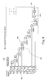
- FIG. 8 is a flowchart of value operation according to one embodiment of the invention.
- FIG. 9 is a schematic view of a 64-set basic sequential decoding system according to one embodiment of the invention.
- FIG. 6 is a schematic view of an apparatus of sequentially decoding CCK codes according one embodiment of the invention.
- the apparatus of the invention is applied to calculate the CCK code correlation in a wireless network.
- the apparatus includes a series of received signal registers 601 , a phase selector 602 , a series of adders 603 , a sequential operation register 604 and a comparing device 605 .
- the received signal registers 601 (X 0 , X 1 , X 2 , X 3 X 4 , X 5 , X 6 , X 7 ) are used to respectively temporarily save the received signals.
- the phase selector 602 is used to select one numeral from 1 ⁇ 1,j or ⁇ j respectively for CCK code of each chip to multiply with the signal register.
- the series of adders 603 (Adder 1 , Adder 2 , Adder 3 , Adder 4 , Adder 5 , Adder 6 and Adder 7 ) is used to sequentially complete the adding operation.
- the series of sequential operation registers 604 (R 0 , R 1 , R 2 , R 3 , R 4 , R 5 , R 6 , and R 7 ) is used to save values obtained from the sequential selecting operation of the phase selectors and the sequential adding operation of the adders, and a comparing device is used to select a maximal value from those saved in the operation registers.
- the comparing device 605 includes a comparator 6051 and a maximum register (R 8 ).
- the comparator 6051 can be a 2-to-1 comparator.
- the received signal registers 601 include a first signal register X 0 , a second signal register X 1 , a third signal register X 2 , a fourth signal register X 3 , a fifth signal register X 4 , a sixth signal register X 5 , a seventh signal register X 6 and an eighth signal register X 7 .
- the sequential operation registers 604 include a first operation register R 0 , a second operation register R 1 , a third operation register R 2 , a fourth operation register R 3 , a fifth operation register R 4 , a sixth operation register R 5 , a seventh operation register R 6 and an eighth operation register R 7 .
- the adders 603 include a first adder Adder 1 , a second Adder 2 , a third adder Adder 3 , a fourth Adder 4 , a fifth Adder 5 , a sixth Adder 6 and a seventh Adder 7 .
- X 0 is subjected to the phase selection and multiplication and then saved in R 0 .
- Adder 1 adds up R 0 and the product of X 1 multiplies with a selected phase (1, ⁇ 1, j, ⁇ j) and saves the obtained sum in R 1 .
- Adder 2 adds up R 1 and the product of X 2 multiplies with a selected phase (1, ⁇ 1, j, ⁇ j), and saves the obtained sum in R 2 .
- Adder 3 adds up R 2 and the product of X 3 multiplies with a selected phase (1, ⁇ 1, j, ⁇ j), and saves the obtained sum in R 3 .
- Adder 4 adds up R 3 and the product of X 4 multiplies with a selected phase (1, ⁇ 1, j, ⁇ j), and saves the obtained sum in R 4 .
- Adder 5 adds up R 4 and the product of X 5 multiplies with a selected phase (1, ⁇ 1, j, ⁇ j), and saves the obtained sum in R 5 .
- Adder 6 adds up R 5 and the product of X 6 multiplies with a selected phase (1, ⁇ 1, j, ⁇ j), and saves the obtained sum in R 6 .
- Adder 7 adds up R 6 and the product of X 7 multiplies with a selected phase (1, ⁇ 1, j, ⁇ j), and saves the obtained sum saved in R 7 .
- the phase selector selects one phase from 1, ⁇ 1, j or ⁇ j according to a first set of CCK codes of a No. 0 chip ( C 0 — 1 ). This product is saved in the first operation register (R 0 ).
- the phase selector selects one phase from 1, ⁇ 1, j or ⁇ j according to a first set of CCK codes of a No. 1 chip (C 1 — 1 ). This product and the value of the first operation register (R 0 ) add up to be saved in the second operation register (R 1 ).
- the phase selector selects a phase from 1, ⁇ 1, j, ⁇ j according to a second set of CCK codes of a No. 0 chip (C 0 — 2 ) to multiply with X 0 .
- the value generated by Adder7 and saved in R7 indicates the correlation between the corresponding received signal and the first CCK codes.
- the corresponding register stops inputting signals and starts repeating the above operations.
- the obtained values generated by Adder 7 and saved in R7 respectively indicate the correlation between the corresponding received signals and the second, third, fourth etc sets of CCK codes. Those obtained values are respectively compared with the currently saved maximal value in the maximum register (R 8 ) and replace the currently saved maximal value if the obtained value is bigger than the currently saved maximal value.
- FIG. 7 illustrates a CCK decoding apparatus according to one embodiment of the invention.
- FIG. 8 is a flowchart of a value operation according to one embodiment of the invention.
- the mean value of R 0 is X 0 C* 0 — 1 .
- the mean value of R 1 is R 0 +X 1 C* 1 — 1 , i.e., X 0 C* 0 — 1 +X 1 C* 1 — 1 and R 0 changes into X 0 C* 0 — 2 .
- the mean value of R 2 is R 1 +X 2 C* 2 — 1 , i.e., X 0 C* 0 — 1 +X 1 C* 1 — 1 +X 2 C* 2 — 1 .
- R 1 changes into R 0 +X 1 C* 1 — 2 , i.e., X 0 C* 0 — 2 +X 1 C* 1 — 2
- R 0 changes into X 0 C* 0 — 3 .
- R 3 is X 0 C* 0 — 1 +X 1 C* 1 — 1 +X 2 C* 2 — 1 +X 3 C* 3 — 1 and R 2 is X 0 C* 0 — 2 +X 1 C* 1 — 2 +X 2 C* 2 — 2, R 1 is X 0 C* 0 — 3 +X 1 C* 1 — 3 and R 0 is into X 0 C* 0 — 4 .
- R 7 indicates the correlation of the first set of CCK codes.
- R 7 indicates the correlation of the second set of CCK codes.
- R 7 indicates the correlation of the eighth set of CCK codes.
- FIG. 5 illustrates a process of sequentially decoding CCK codes according to one embodiment of the invention.
- a first input signal is received and saved in the first signal register (X 0 ) and the phase selector selects one phase from 1, ⁇ 1, j or ⁇ j according to the first set of CCK codes of a No. 0 chip (C 0 — 1 ), this product is saved in the first operation register (R 0 ) (step 501 ).
- a second input signal is received and saved in the second signal register (X 1 ), and multiplies with 1, ⁇ 1,j or ⁇ j according to a first set of CCK codes of a No. 1 chip (C 1 — 1 ).
- a third input signal is received and saved in the third signal register (X 2 ), and multiplies with 1, ⁇ 1, j or ⁇ j according to a first set of CCK codes of a No. 2 chip(C 2 — 1 ).
- a fourth input signal is received and saved in the fourth signal register (X 3 ), and multiplies with 1, ⁇ 1, j or ⁇ j according to a first set of CCK codes of a No. 3 chip (C 3 — 1 ).
- This product and the value of the third operation register (R 2 ) add up to be saved in the fourth operation register (R 3 ) (step 504 ).
- a fifth input signal is received and saved in the fifth signal register(X 4 ), and multiplies with 1, ⁇ 1, j or ⁇ j according to a first set of CCK codes of a No. 4 chip (C 4 — 1 ).
- This product and the value of the fourth operation register (R 3 ) add up to be saved in the fifth operation register (R 4 ) (step 505 ).
- a sixth input signal is received and saved in the sixth signal register (X 5 ), and multiplies with 1, ⁇ 1, j or ⁇ j according to a first set of CCK codes of a No. 5 chip (C 5 — 1 ).
- This product and the value of the fifth operation register (R 4 ) add up to be saved in the sixth operation register (R 5 ) (step 506 ).
- a seventh input signal is received and saved in the seventh signal register (X 6 ), and multiplies with 1, ⁇ 1,j or ⁇ j according to a first set of CCK codes of a No. 6 chip (C 6 — 1 ).
- This product and the value of the sixth operation register (R 5 ) add up to be saved in the seventh operation register (R 6 ) (step 507 ).
- An eighth input signal is received and saved in the eighth signal register(X 7 ), and multiplies with 1, ⁇ 1,j or ⁇ j according to a first set of CCK codes of a No.
- R 7 indicates the correlation between the corresponding values and the first sets of CCK codes.
- one of 1, ⁇ 1, j, or ⁇ j is selected according to a second set of CCK codes of a No. 0 chip(C 0 — 2 ) to multiply with the first signal register (X 0 ), the product is saved in the first operation register (R 0 ).
- one of 1, ⁇ 1, j, or ⁇ j is selected according to a second set of CCK codes of a No. 1 chip (C 1 — 2 ) to multiply with the value of the second signal register (X 1 ).
- the product and the first operation register (R 0 ) add up to be saved in the second operation register (R 1 ).
- one of 1, ⁇ 1,j, or ⁇ j is selected according to a second set of CCK codes of a No. 2 chip (C 2 — 2 ) to multiple with the value of the third signal register (X 2 ).
- the product and the second operation register (R 1 ) add up to save in the third operation register (R 2 ).
- one of 1, ⁇ 1, j, or ⁇ j is selected according to a second set of CCK codes of No. 3 chip (C 3 — 2 ) to multiply with the value of the fourth signal register (X 3 ).
- the product and the third operation register (R 2 ) add up to be saved in the fourth operation register (R 3 ).
- one of 1, ⁇ 1, j, or ⁇ j is selected according to a second set of CCK codes of a No. 4 chip (C 4 — 2 ) to multiply with the value of the fifth signal register (X 4 ).
- the product and the fourth operation register (R 3 ) add up to be saved in the fifth operation register (R 4 ).
- one of 1, ⁇ 1, j, or ⁇ j is selected according to a second set of CCK codes of No. 5 chip (C 5 — 2 ) to multiply with the value of the sixth signal register (X 5 ).
- the product and the fifth operation register (R 4 ) add up to be saved in the sixth operation register (R 5 ).
- one of 1, ⁇ 1, j, or ⁇ j is selected according to a second set of CCK codes of No. 6 chip (C 6 — 2 ) to multiply with the value of the seventh signal register (X 6 ).
- the product and the sixth operation register (R 5 ) add up to be saved in the seventh operation register (R 6 ).
- One of 1, ⁇ 1, j, or ⁇ j is selected according to a second set of CCK codes of a No. 7 chip (C 7 — 2 ) to multiply with the value of the eighth signal register (X 7 ).
- the product and the sixth operation register (R 6 ) add up to be saved in the eighth operation register (R 7 ).
- the value saved in R 7 indicates the correlation between the received signals and the second sets of CCK codes.
- one of 1, ⁇ 1, j, or ⁇ j is selected according to a third set of CCK codes of a No. 0 chip (C 0 — 3 ) to multiply with the value of the first signal register (X 0 ).
- the product is saved in the first operation register (R 0 ).
- one of 1, ⁇ 1,j, or ⁇ j is selected according to a third set of CCK codes of a No. 1 chip(C 1 — 3 ) to multiply with the value of the second signal register (X 1 ).
- the product and the first operation register (R 0 ) add up to be saved in the second operation register (R 1 ).
- one of 1, ⁇ 1,j, or ⁇ j is selected according to a third set of CCK codes of a No. 2 chip (C 2 — 3 ) to multiply with the value of the third signal register (X 2 ).
- the product and the second operation register (R 1 ) add up to be saved in the third operation register (R 2 ).
- one of 1, ⁇ 1, j, or ⁇ j is selected according to a third set of CCK codes of a No. 3 chip (C 3 — 3 ) to multiply with the value of the fourth signal register (X 3 ).
- the product and the value of the third operation register (R 2 ) add up to be saved in the fourth operation register (R 3 ).
- one of 1, ⁇ 1, j, or ⁇ j is selected according to a third set of CCK codes of a No. 4 chip (C 4 — 3 ) to multiply with the value of the fifth signal register (X 4 ).
- the product and the value of the fourth operation register (R 3 ) add up to be saved in the fifth operation register (R 4 ).
- one of 1, ⁇ 1, j, or ⁇ j is selected according to a third set of CCK codes of a No. 5 chip (C 5 — 3 ) to multiply with the value of the sixth signal register (X 5 ).
- the product and the value of the fifth operation register (R 4 ) add up to be saved in the sixth operation register (R 5 ).
- One of 1, ⁇ 1, j, or ⁇ j is selected according to a third set of CCK codes of a No. 6 chip (C 6 — 3 ) to multiply with the value of the seventh signal register (X 6 ).
- the product and the value of the sixth operation register (R 5 ) add up to be saved in the seventh operation register (R 6 ).
- One of 1, ⁇ 1, j, or ⁇ j is selected according to a third set of CCK codes of a No. 7 chip (C 7 — 3 ) to multiply with the eighth signal register (X 7 ).
- the product and the value of the seventh operation register (R 6 ) add up to be saved in the eighth operation register (R 7 ).
- the value saved in R 7 indicates the correlation between the received signals and the third sets of CCK codes.
- one of 1, ⁇ 1,j, or ⁇ j is selected according to a fourth set of CCK codes of a No. 0 chip (C 0 — 4 ) to multiply with the value of a first signal register (X 0 ).
- the product is saved in the first operation register (R 0 ).
- one of 1, ⁇ 1, j, or ⁇ j is selected according to a fourth set of CCK codes of a No. 1 chip (C 1 — 4 ) to multiply with the second signal register (X 1 ).
- the product and the value of the first operation register (R 0 ) add up to be saved in the second operation register (R 1 ).
- one of 1, ⁇ 1, j, or ⁇ j is selected according to a fourth set of CCK codes of a No. 2 chip (C 2 — 4 ) to multiply with the third signal register (X 2 ).
- the product and the second operation register (R 1 ) add up to be saved in the third operation register (R 2 ).
- one of 1, ⁇ 1, j, or ⁇ j is selected according to a fourth set of CCK codes of a No. 3 chip (C 3 — 4 ) to multiply with the fourth signal register (X 3 ).
- the product and the third operation register (R 2 ) add up to be saved in the fourth operation register (R 3 ).
- one of 1, ⁇ 1, j, or ⁇ j is selected according to a fourth set of CCK codes of a No. 4 chip (C 4 — 4 ) to multiply with the fifth signal register (X 4 ).
- the product and the fourth operation register (R 3 ) add up to be saved in the fifth operation register (R 4 ).
- One of 1, ⁇ 1, j, or ⁇ j is selected according to a fourth set of CCK codes of a No. 5 chip (C 5 — 4 ) to multiply with the sixth signal register (X 5 ).
- the product and the fifth operation register (R 4 ) add up to be saved in the sixth operation register (R 5 ).
- One of 1, ⁇ 1, j, or ⁇ j is selected according to a fourth set of CCK codes of a No. 6 chip (C 6 — 4 )to multiply with the seventh signal register(X 6 ).
- the product and the sixth operation register (R 5 ) add up to be saved in the seventh operation register (R 6 ).
- One of 1, ⁇ 1, j, or ⁇ j is selected according to a fourth set of CCK codes of a No. 7 chip (C 7 — 4 ) to multiply with the eighth signal register (X 7 ).
- the product and the seventh operation register (R 6 ) add up to be saved in the eighth operation register (R 7 ).
- the value saved in R 7 indicates the correlation between the received signals and the fourth sets of CCK codes.
- one of 1, ⁇ 1, j, or ⁇ j is selected according to a fifth set of CCK codes of a No. 0 chip (C 0 — 5 ) to multiply with the first signal register (X 0 ).
- the product is saved in the first operation register (R 0 ).
- one of 1, ⁇ 1, j, or ⁇ j is selected according to a fifth set of CCK codes of a No. 1 chip (C 1 — 5 ) to multiply with the second signal register (X 1 ).
- the product and the first operation register (R 0 ) add up to be saved in the second operation register (R 1 ).
- one of 1, ⁇ 1, j, or ⁇ j is selected according to a fifth set of CCK codes of a No. 2 chip (C 2 — 5 ) to multiply with the third signal register (X 2 ).
- the product and the second operation register (R 1 ) add up to be saved in the third operation register (R 2 ).
- one of 1, ⁇ 1, j, or ⁇ j is selected according to a fifth set of CCK codes of a No. 3 chip (C 3 — 5 ) to multiply with the fourth signal register (X 3 ).
- the product and the third operation register (R 2 ) add up to be saved in the fourth operation register (R 3 ).
- One of 1, ⁇ 1, j, or ⁇ j is selected according to a fifth set of CCK codes of a No. 4 chip (C 4 — 5 ) to multiply with the fifth signal register (X 4 ).
- the product and the fourth operation register (R 3 ) add up to be saved in the fifth operation register (R 4 ).
- One of 1, ⁇ 1, j, or ⁇ j is selected according to a fifth set of CCK codes of a No. 5 chip (C 5 — 5 ) to multiply with the sixth signal register (X 5 ).
- the product and the fifth operation register (R 4 ) add up to be saved in the sixth operation register (R 5 ).
- One of 1, ⁇ 1, j, or ⁇ j is selected according to a fifth set of CCK codes of a No. 6 chip (C 6 — 5 )to multiply with the seventh signal register(X 6 ).
- the product and the sixth operation register (R 5 ) add up to be saved in the seventh operation register (R 6 ).
- One of 1, ⁇ 1, j, or ⁇ j is selected according to a fifth set of CCK codes of a No. 7 chip (C 7 — 5 ) to multiply with the eighth signal register (X 7 ).
- the product and the seventh operation register (R 6 ) add up to be saved in the eighth operation register (R 7 ).
- the value saved in R 7 indicates the correlation between the received signals and the fifth sets of CCK codes.
- one of 1, ⁇ 1, j, or ⁇ j is selected according to a sixth set of CCK codes of a No. 0 chip (C 0 — 6 ) to multiply with the first signal register (X 0 ).
- the product is saved in the first operation register (R 0 ).
- one of 1, ⁇ 1, j, or ⁇ j is selected according to a sixth set of CCK codes of a No. 1 chip (C 1 — 6 ) to multiply with the second signal register (X 1 ).
- the product and the first operation register (R 0 ) add up to be saved in the second operation register (R 1 ).
- one of 1, ⁇ 1,j, or ⁇ j is selected according to a sixth set of CCK codes of a No. 2 chip(C 2 — 6 )to multiply with the third signal register(X 2 ).
- the product and the second operation register (R 1 ) add up to be saved in the third operation register (R 2 ).
- One of 1, ⁇ 1, j, or ⁇ j is selected according to a sixth set of CCK codes of a No. 3 chip (C 3 — 6 ) to multiply with the fourth signal register (X 3 ).
- the product and the third operation register (R 2 ) add up to be saved in the fourth operation register (R 3 ).
- One of 1, ⁇ 1, j, or ⁇ j is selected according to a sixth set of CCK codes of a No. 4 chip (C 4 — 6 ) to multiply with the fifth signal register (X 4 ).
- the product and the fourth operation register (R 3 ) add up to be saved in the fifth operation register (R 4 ).
- One of 1, ⁇ 1, j, or ⁇ j is selected according to a sixth set of CCK codes of a No. 5 chip (C 5 — 6 ) to multiply with the sixth signal register (X 5 ).
- the product and the fifth operation register (R 4 ) add up to be saved in the sixth operation register (R 5 ).
- One of 1, ⁇ 1, j, or ⁇ j is selected according to a sixth set of CCK codes of a No. 6 chip (C 6 — 6 )to multiply with the seventh signal register(X 6 ).
- the product and the sixth operation register (R 5 ) add up to be saved in the seventh operation register (R 6 ).
- One of 1, ⁇ 1, j, or ⁇ j is selected according to a sixth set of CCK codes of a No. 7 chip (C 7 — 6 ) to multiply with the eighth signal register (X 7 ).
- the product and the seventh operation register (R 6 ) add up to be saved in the eighth operation register (R 7 ).
- the value saved in R 7 indicates the correlation between the received signals and the sixth sets of CCK codes.
- one of 1, ⁇ 1, j, or ⁇ j is selected according to a seventh set of CCK codes of a No. 0 chip (C 0 — 7 ) to multiply with the first signal register (X 0 ).
- the product is saved in the first operation register (R 0 ).
- one of 1, ⁇ 1, j, or ⁇ j is selected according to a seventh set of CCK codes of a No. 1 chip (C 1 — 7 ) to multiply with the second signal register (X 1 ).
- the product and the first operation register (R 0 ) add up to be saved in the second operation register (R 1 ).
- One of 1, ⁇ 1, j, or ⁇ j is selected according to a seventh set of CCK codes of a No. 2 chip (C 2 — 7 ) to multiply with the third signal register (X 2 ).
- the product and the second operation register (R 1 ) add up to be saved in the third operation register (R 2 ).
- One of 1, ⁇ 1, j, or ⁇ j is selected according to a seventh set of CCK codes of a No. 3 chip (C 3 — 7 ) to multiply with the fourth signal register (X 3 ).
- the product and the third operation register (R 2 ) add up to be saved in the fourth operation register (R 3 ).
- One of 1, ⁇ 1, j, or ⁇ j is selected according to a seventh set of CCK codes of a No. 4 chip (C 4 — 7 ) to multiply with the fifth signal register (X 4 ).
- the product and the fourth operation register (R 3 ) add up to be saved in the fifth operation register (R 4 ).
- One of 1, ⁇ 1, j, or ⁇ j is selected according to a seventh set of CCK codes of a No. 5 chip (C 5 — 7 ) to multiply with the sixth signal register (X 5 ).
- the product and the fifth operation register (R 4 ) add up to be saved in the sixth operation register (R 5 ).
- One of 1, ⁇ 1, j, or ⁇ j is selected according to a seventh set of CCK codes of a No. 6 chip (C 6 — 7 )to multiply with the seventh signal register(X 6 ).
- the product and the sixth operation register (R 5 ) add up to be saved in the seventh operation register (R 6 ).
- One of 1, ⁇ 1, j, or ⁇ j is selected according to a seventh set of CCK codes of a No. 7 chip (C 7 — 7 ) to multiply with the eighth signal register (X 7 ).
- the product and the seventh operation register (R 6 ) add up to be saved in the eighth operation register (R 7 ).
- the value saved in R 7 indicates the correlation between the received signals and the seventh sets of CCK codes.
- one of 1, ⁇ 1, j, or ⁇ j is selected according to an eighth seventh set of CCK codes of a No. 0 chip (C 0 — 8 ) to multiply with the first signal register (X 0 ).
- the product is saved in the first operation register (R 0 ).
- One of 1, ⁇ 1, j, or ⁇ j is selected according to an eighth set of CCK codes of a No. 1 chip (C 1 — 8 ) to multiply with the second signal register (X 1 ).
- the product and the first operation register (R 0 ) add up to be saved in the second operation register (R 1 ).
- One of 1, ⁇ 1, j, or ⁇ j is selected according to an eighth set of CCK codes of a No. 2 chip (C 2 — 8 ) to multiply with the third signal register (X 2 ).
- the product and the second operation register (R 1 ) add up to be saved in the third operation register (R 2 ).
- One of 1, ⁇ 1, j, or ⁇ j is selected according to an eighth set of CCK codes of a No. 3 chip (C 3 — 8 ) to multiply with the fourth signal register (X 3 ).
- the product and the third operation register (R 2 ) add up to be saved in the fourth operation register (R 3 ).
- One of 1, ⁇ 1, j, or ⁇ j is selected according to an eighth set of CCK codes of a No. 4 chip (C 4 — 8 ) to multiply with the fifth signal register (X 4 ).
- the product and the fourth operation register (R 3 ) add up to be saved in the fifth operation register (R 4 ).
- One of 1, ⁇ 1, j, or ⁇ j is selected according to an eighth set of CCK codes of a No. 5 chip (C 5 — 8 ) to multiply with the sixth signal register (X 5 ).
- the product and the fifth operation register (R 4 ) add up to be saved in the sixth operation register (R 5 ).
- One of 1, ⁇ 1, j, or ⁇ j is selected according to an eighth set of CCK codes of a No. 6 chip (C 6 — 8 )to multiply with the seventh signal register(X 6 ).
- the product and the sixth operation register (R 5 ) add up to be saved in the seventh operation register (R 6 ).
- One of 1, ⁇ 1, j, or ⁇ j is selected according to an eighth set of CCK codes of a No. 7 chip (C 7 — 8 ) to multiply with the eighth signal register (X 7 ).
- the product and the seventh operation register (R 6 ) add up to be saved in the eighth operation register (R 7 ).
- the value saved in R 7 indicates the correlation between the received signals and the eighth sets of CCK codes.
- the maximal one is chosen among the values respectively indicating the received signals and the corresponding sets of CCK codes and then saved in the maximum register (R 8 ).
- a first correlation value is obtained at step 508 . Therefore, the first correlation value is the maximal one and should be saved in the maximum register R 8 .
- a second correlation value is obtained at the next clock R 7 . Then the second correlation value is compared with the currently maximal value saved in R 8 , and the bigger one is saved in R 8 . Repeat this operation until the comparison for all the correlation values have done.
- FIG. 9 is a schematic view of a 64-set basic sequential decoding system applied in the correlation calculation of CCK codes in wireless network to decode IEEE802.11b/g-standard 11M CCK codes according to one embodiment of the invention. It is noted that the system of the invention can be also applied in decoding IEEE802.11b/g-standard 5.5M CCK codes to reduce the hardware complexity.
- the system includes a series of received signal registers 901 , and a first to eighth basic sequential decoding modules 902 , 903 , 904 . . . 909 .
- the series of received signal registers 901 (X 0 , X 1 , X 2 , X 3 , X 4 , X 5 , X 6 , X 7 ) are used to respectively temporarily save the received signals.
- the first to eighth basic sequentially decoding modules 902 , 903 . . . 909 are used to sequentially decode CCK codes according to the received signals.
- Each basic sequentially decoding module includes:
- the received signal registers include a first signal register X 0 , a second signal register X 1 , a third signal register X 2 , a fourth signal register X 3 , a fifth signal register X 4 , a sixth signal register X 5 , a seventh signal register X 6 and a eighth signal register X 7 .
- the sequential operation registers include a first operation register R 0 , a second operation register R 1 , a third operation register R 2 , a fourth operation register R 3 , a fifth operation register R 4 , a sixth operation register R 5 , a seventh operation register R 6 and a eighth operation register R 7 .
- the adders include a first adder Adder 1 , a second Adder 2 , a third adder Adder 3 , a fourth Adder 4 , a fifth Adder 5 , a sixth Adder 6 and a seventh Adder 7 .
- Adder 1 adds up R 0 and the product of X 1 multiplies with a selected phase (1, ⁇ 1, j, ⁇ j) and saves the obtained sum in R 1 .
- Adder 2 adds up R 1 and the product of X 2 multiplies with a selected phase (1, ⁇ 1, j, ⁇ j), and saves the obtained sum in R 2 .
- Adder 3 adds up R 2 and the product of X 3 multiplies with a selected phase (1, ⁇ 1, j, ⁇ j), and saves the obtained sum in R 3 .
- Adder 4 adds up R 3 and the product of X 4 multiplies with a selected phase (1, ⁇ 1, j, ⁇ j), and saves the obtained sum in R 4 .
- Adder 5 adds up R 4 and the product of X 5 multiplies with a selected phase (1, ⁇ 1, j, ⁇ j), and saves the obtained sum in R 5 .
- Adder 6 adds up R 5 and the product of X 6 multiplies with a selected phase (1, ⁇ 1, j, ⁇ j), and saves the obtained sum in R 6 .
- Adder 7 adds up R 6 and the product of X 7 multiplies with a selected phase (1, ⁇ 1, j, ⁇ j), and saves the obtained sum saved in R 7 .
Abstract
Description
r0*C*0
wherein r0 . . . r7 is the received signals, C0
C={exp j(Φ1+Φ2+Φ3+Φ4), exp j(Φ1+Φ3+Φ4), exp j(Φ1+Φ2+Φ4), −exp j(Φ1+Φ4), exp j(Φ1+Φ2+Φ3), exp j(Φ1+Φ3), −exp j(Φ1+Φ2), exp j(Φ1)}
-
- a phase selector, used to select one phase from 1, −1, j, −j for each chip to sequentially multiply with the series of registers;
- a series of adders (Adder1, Adder2, Adder3, Adder4, Adder5, Adder6 and Adder7) used to sequentially complete the addition operation;
- a series of sequential operation registers (R0, R1, R2, R3, R4, R5, R6, R7) used to save values obtained from the sequential selecting operation of the phase selectors and the sequential adding operation of the adders; and
- a comparing device used to select a maximal value from those saved in the operation registers. The comparing device includes a comparator and a maximum register (R8). The comparator can be a 2-to-1 comparator.
Claims (13)
Priority Applications (1)
| Application Number | Priority Date | Filing Date | Title |
|---|---|---|---|
| US10/819,319 US7330522B2 (en) | 2004-04-07 | 2004-04-07 | Complementary code keying (CCK) sequentially decoding apparatus and process thereof |
Applications Claiming Priority (1)
| Application Number | Priority Date | Filing Date | Title |
|---|---|---|---|
| US10/819,319 US7330522B2 (en) | 2004-04-07 | 2004-04-07 | Complementary code keying (CCK) sequentially decoding apparatus and process thereof |
Publications (2)
| Publication Number | Publication Date |
|---|---|
| US20050226351A1 US20050226351A1 (en) | 2005-10-13 |
| US7330522B2 true US7330522B2 (en) | 2008-02-12 |
Family
ID=35060523
Family Applications (1)
| Application Number | Title | Priority Date | Filing Date |
|---|---|---|---|
| US10/819,319 Active 2026-03-16 US7330522B2 (en) | 2004-04-07 | 2004-04-07 | Complementary code keying (CCK) sequentially decoding apparatus and process thereof |
Country Status (1)
| Country | Link |
|---|---|
| US (1) | US7330522B2 (en) |
Families Citing this family (1)
| Publication number | Priority date | Publication date | Assignee | Title |
|---|---|---|---|---|
| WO2006004550A2 (en) * | 2004-07-06 | 2006-01-12 | Telefonaktiebolaget Lm Ericsson (Publ) | Non-contiguous variable length orthogonal codes |
Citations (7)
| Publication number | Priority date | Publication date | Assignee | Title |
|---|---|---|---|---|
| US20020122466A1 (en) | 2000-12-29 | 2002-09-05 | Somayazulu V. S. | Fast transform system for an extended data rate WLAN system |
| US6674818B1 (en) * | 2000-04-17 | 2004-01-06 | Rf Micro Devices, Inc. | Reduced complexity decision circuitry |
| US20040071104A1 (en) * | 2002-07-03 | 2004-04-15 | Commasic, Inc. | Multi-mode method and apparatus for performing digital modulation and demodulation |
| US20040086062A1 (en) * | 2002-10-31 | 2004-05-06 | Advanced Micro Devices, Inc. | Complementary code decoding by reduced sized circuits |
| US20040230628A1 (en) * | 2000-11-14 | 2004-11-18 | Rawlins Gregory S. | Methods, systems, and computer program products for parallel correlation and applications thereof |
| US20050185741A1 (en) * | 2000-11-14 | 2005-08-25 | Parkervision, Inc. | Method and apparatus for a parallel correlator and applications thereof |
| US20060115024A1 (en) * | 2004-11-29 | 2006-06-01 | Mau-Lin Wu | Fast Walsh transform (FWT) demodulator and method thereof |
-
2004
- 2004-04-07 US US10/819,319 patent/US7330522B2/en active Active
Patent Citations (9)
| Publication number | Priority date | Publication date | Assignee | Title |
|---|---|---|---|---|
| US6674818B1 (en) * | 2000-04-17 | 2004-01-06 | Rf Micro Devices, Inc. | Reduced complexity decision circuitry |
| US20040230628A1 (en) * | 2000-11-14 | 2004-11-18 | Rawlins Gregory S. | Methods, systems, and computer program products for parallel correlation and applications thereof |
| US20050185741A1 (en) * | 2000-11-14 | 2005-08-25 | Parkervision, Inc. | Method and apparatus for a parallel correlator and applications thereof |
| US7010559B2 (en) * | 2000-11-14 | 2006-03-07 | Parkervision, Inc. | Method and apparatus for a parallel correlator and applications thereof |
| US7233969B2 (en) * | 2000-11-14 | 2007-06-19 | Parkervision, Inc. | Method and apparatus for a parallel correlator and applications thereof |
| US20020122466A1 (en) | 2000-12-29 | 2002-09-05 | Somayazulu V. S. | Fast transform system for an extended data rate WLAN system |
| US20040071104A1 (en) * | 2002-07-03 | 2004-04-15 | Commasic, Inc. | Multi-mode method and apparatus for performing digital modulation and demodulation |
| US20040086062A1 (en) * | 2002-10-31 | 2004-05-06 | Advanced Micro Devices, Inc. | Complementary code decoding by reduced sized circuits |
| US20060115024A1 (en) * | 2004-11-29 | 2006-06-01 | Mau-Lin Wu | Fast Walsh transform (FWT) demodulator and method thereof |
Also Published As
| Publication number | Publication date |
|---|---|
| US20050226351A1 (en) | 2005-10-13 |
Similar Documents
| Publication | Publication Date | Title |
|---|---|---|
| US7010559B2 (en) | Method and apparatus for a parallel correlator and applications thereof | |
| US7391632B2 (en) | Apparatus of selectively performing fast hadamard transform and fast fourier transform, and CCK modulation and demodulation apparatus using the same | |
| JP2526510B2 (en) | Wireless data communication device | |
| US20060067413A1 (en) | Multicode transmission using Walsh Hadamard transform | |
| US7454453B2 (en) | Methods, systems, and computer program products for parallel correlation and applications thereof | |
| EP0782288A2 (en) | Spread spectrum communication system | |
| US20070014271A1 (en) | Packet Detection Device | |
| US20100272157A1 (en) | Spread spectrum encoding and decoding | |
| US8537878B2 (en) | Spread-spectrum codes generation | |
| US20030161278A1 (en) | Symbol data converting circuit | |
| US7532691B2 (en) | Parallel architecture digital filter and spread spectrum signal receiver using such a filter | |
| US7330522B2 (en) | Complementary code keying (CCK) sequentially decoding apparatus and process thereof | |
| US7457357B2 (en) | Decision feedback equalizer design with interference removal and reduced error propagation | |
| US8958459B2 (en) | Method and apparatus for despread data in wireless communication system | |
| US6529546B2 (en) | Acquisition of a spread-spectrum signal using counters | |
| US7263131B2 (en) | OFDM-based timing synchronization detection apparatus and method | |
| US6993541B2 (en) | Fast hadamard peak detector | |
| JP3156783B2 (en) | Synchronization acquisition device and synchronization acquisition method in spread spectrum communication system | |
| EP1324505A1 (en) | Spreading code assigning method and base transceiver station | |
| US8077756B2 (en) | Signal transmitting method, transmitting apparatus, and receiving apparatus used for the signal transmitting method | |
| US6928105B2 (en) | Vector tree correlator for variable spreading rates | |
| Rajagopal et al. | On-line arithmetic for detection in digital communication receivers | |
| KR100577005B1 (en) | Apparatus and method of selectively performing fast hadamard transform and fast fourier transform | |
| US7184496B2 (en) | Complementary code decoding by reduced sized circuits | |
| JP6522248B1 (en) | Receiving device, communication system, and method of calculating likelihood of modulated signal |
Legal Events
| Date | Code | Title | Description |
|---|---|---|---|
| AS | Assignment |
Owner name: INTERGRATED SYSTEM SOLUTION CORP., TAIWAN Free format text: ASSIGNMENT OF ASSIGNORS INTEREST;ASSIGNORS:HUANG, CHEN-YEN;MA, KUANG-PING;LIN, CHUN-CHANG;AND OTHERS;REEL/FRAME:015184/0661 Effective date: 20040318 |
|
| STCF | Information on status: patent grant |
Free format text: PATENTED CASE |
|
| FPAY | Fee payment |
Year of fee payment: 4 |
|
| AS | Assignment |
Owner name: ISSC TECHNOLOGIES CORP., TAIWAN Free format text: CHANGE OF NAME;ASSIGNOR:INTEGRATED SYSTEM SOLUTION CORP.;REEL/FRAME:027082/0905 Effective date: 20100610 |
|
| FPAY | Fee payment |
Year of fee payment: 8 |
|
| AS | Assignment |
Owner name: MICROCHIP TECHNOLOGY (BARBADOS) II INCORPORATED, C Free format text: MERGER;ASSIGNOR:ISSC TECHNOLOGIES CORP.;REEL/FRAME:036561/0892 Effective date: 20150530 |
|
| AS | Assignment |
Owner name: MICROCHIP TECHNOLOGY INCORPORATED, ARIZONA Free format text: ASSIGNMENT OF ASSIGNORS INTEREST;ASSIGNOR:MICROCHIP TECHNOLOGY (BARBADOS) II INCORPORATED;REEL/FRAME:036631/0442 Effective date: 20150601 |
|
| FEPP | Fee payment procedure |
Free format text: PAT HOLDER NO LONGER CLAIMS SMALL ENTITY STATUS, ENTITY STATUS SET TO UNDISCOUNTED (ORIGINAL EVENT CODE: STOL); ENTITY STATUS OF PATENT OWNER: LARGE ENTITY |
|
| AS | Assignment |
Owner name: JPMORGAN CHASE BANK, N.A., AS ADMINISTRATIVE AGENT, ILLINOIS Free format text: SECURITY INTEREST;ASSIGNOR:MICROCHIP TECHNOLOGY INCORPORATED;REEL/FRAME:041675/0617 Effective date: 20170208 Owner name: JPMORGAN CHASE BANK, N.A., AS ADMINISTRATIVE AGENT Free format text: SECURITY INTEREST;ASSIGNOR:MICROCHIP TECHNOLOGY INCORPORATED;REEL/FRAME:041675/0617 Effective date: 20170208 |
|
| AS | Assignment |
Owner name: JPMORGAN CHASE BANK, N.A., AS ADMINISTRATIVE AGENT, ILLINOIS Free format text: SECURITY INTEREST;ASSIGNORS:MICROCHIP TECHNOLOGY INCORPORATED;SILICON STORAGE TECHNOLOGY, INC.;ATMEL CORPORATION;AND OTHERS;REEL/FRAME:046426/0001 Effective date: 20180529 Owner name: JPMORGAN CHASE BANK, N.A., AS ADMINISTRATIVE AGENT Free format text: SECURITY INTEREST;ASSIGNORS:MICROCHIP TECHNOLOGY INCORPORATED;SILICON STORAGE TECHNOLOGY, INC.;ATMEL CORPORATION;AND OTHERS;REEL/FRAME:046426/0001 Effective date: 20180529 |
|
| AS | Assignment |
Owner name: WELLS FARGO BANK, NATIONAL ASSOCIATION, AS NOTES COLLATERAL AGENT, CALIFORNIA Free format text: SECURITY INTEREST;ASSIGNORS:MICROCHIP TECHNOLOGY INCORPORATED;SILICON STORAGE TECHNOLOGY, INC.;ATMEL CORPORATION;AND OTHERS;REEL/FRAME:047103/0206 Effective date: 20180914 Owner name: WELLS FARGO BANK, NATIONAL ASSOCIATION, AS NOTES C Free format text: SECURITY INTEREST;ASSIGNORS:MICROCHIP TECHNOLOGY INCORPORATED;SILICON STORAGE TECHNOLOGY, INC.;ATMEL CORPORATION;AND OTHERS;REEL/FRAME:047103/0206 Effective date: 20180914 |
|
| MAFP | Maintenance fee payment |
Free format text: PAYMENT OF MAINTENANCE FEE, 12TH YEAR, LARGE ENTITY (ORIGINAL EVENT CODE: M1553); ENTITY STATUS OF PATENT OWNER: LARGE ENTITY Year of fee payment: 12 |
|
| AS | Assignment |
Owner name: JPMORGAN CHASE BANK, N.A., AS ADMINISTRATIVE AGENT, DELAWARE Free format text: SECURITY INTEREST;ASSIGNORS:MICROCHIP TECHNOLOGY INC.;SILICON STORAGE TECHNOLOGY, INC.;ATMEL CORPORATION;AND OTHERS;REEL/FRAME:053311/0305 Effective date: 20200327 |
|
| AS | Assignment |
Owner name: ATMEL CORPORATION, ARIZONA Free format text: RELEASE BY SECURED PARTY;ASSIGNOR:JPMORGAN CHASE BANK, N.A, AS ADMINISTRATIVE AGENT;REEL/FRAME:053466/0011 Effective date: 20200529 Owner name: MICROCHIP TECHNOLOGY INC., ARIZONA Free format text: RELEASE BY SECURED PARTY;ASSIGNOR:JPMORGAN CHASE BANK, N.A, AS ADMINISTRATIVE AGENT;REEL/FRAME:053466/0011 Effective date: 20200529 Owner name: SILICON STORAGE TECHNOLOGY, INC., ARIZONA Free format text: RELEASE BY SECURED PARTY;ASSIGNOR:JPMORGAN CHASE BANK, N.A, AS ADMINISTRATIVE AGENT;REEL/FRAME:053466/0011 Effective date: 20200529 Owner name: MICROSEMI STORAGE SOLUTIONS, INC., ARIZONA Free format text: RELEASE BY SECURED PARTY;ASSIGNOR:JPMORGAN CHASE BANK, N.A, AS ADMINISTRATIVE AGENT;REEL/FRAME:053466/0011 Effective date: 20200529 Owner name: MICROSEMI CORPORATION, CALIFORNIA Free format text: RELEASE BY SECURED PARTY;ASSIGNOR:JPMORGAN CHASE BANK, N.A, AS ADMINISTRATIVE AGENT;REEL/FRAME:053466/0011 Effective date: 20200529 |
|
| AS | Assignment |
Owner name: WELLS FARGO BANK, NATIONAL ASSOCIATION, MINNESOTA Free format text: SECURITY INTEREST;ASSIGNORS:MICROCHIP TECHNOLOGY INC.;SILICON STORAGE TECHNOLOGY, INC.;ATMEL CORPORATION;AND OTHERS;REEL/FRAME:053468/0705 Effective date: 20200529 |
|
| AS | Assignment |
Owner name: WELLS FARGO BANK, NATIONAL ASSOCIATION, AS COLLATERAL AGENT, MINNESOTA Free format text: SECURITY INTEREST;ASSIGNORS:MICROCHIP TECHNOLOGY INCORPORATED;SILICON STORAGE TECHNOLOGY, INC.;ATMEL CORPORATION;AND OTHERS;REEL/FRAME:055671/0612 Effective date: 20201217 |
|
| AS | Assignment |
Owner name: WELLS FARGO BANK, NATIONAL ASSOCIATION, AS NOTES COLLATERAL AGENT, MINNESOTA Free format text: SECURITY INTEREST;ASSIGNORS:MICROCHIP TECHNOLOGY INCORPORATED;SILICON STORAGE TECHNOLOGY, INC.;ATMEL CORPORATION;AND OTHERS;REEL/FRAME:057935/0474 Effective date: 20210528 |
|
| AS | Assignment |
Owner name: MICROSEMI STORAGE SOLUTIONS, INC., ARIZONA Free format text: RELEASE BY SECURED PARTY;ASSIGNOR:JPMORGAN CHASE BANK, N.A., AS ADMINISTRATIVE AGENT;REEL/FRAME:059333/0222 Effective date: 20220218 Owner name: MICROSEMI CORPORATION, ARIZONA Free format text: RELEASE BY SECURED PARTY;ASSIGNOR:JPMORGAN CHASE BANK, N.A., AS ADMINISTRATIVE AGENT;REEL/FRAME:059333/0222 Effective date: 20220218 Owner name: ATMEL CORPORATION, ARIZONA Free format text: RELEASE BY SECURED PARTY;ASSIGNOR:JPMORGAN CHASE BANK, N.A., AS ADMINISTRATIVE AGENT;REEL/FRAME:059333/0222 Effective date: 20220218 Owner name: SILICON STORAGE TECHNOLOGY, INC., ARIZONA Free format text: RELEASE BY SECURED PARTY;ASSIGNOR:JPMORGAN CHASE BANK, N.A., AS ADMINISTRATIVE AGENT;REEL/FRAME:059333/0222 Effective date: 20220218 Owner name: MICROCHIP TECHNOLOGY INCORPORATED, ARIZONA Free format text: RELEASE BY SECURED PARTY;ASSIGNOR:JPMORGAN CHASE BANK, N.A., AS ADMINISTRATIVE AGENT;REEL/FRAME:059333/0222 Effective date: 20220218 |
|
| AS | Assignment |
Owner name: MICROCHIP TECHNOLOGY INCORPORATED, ARIZONA Free format text: RELEASE BY SECURED PARTY;ASSIGNOR:JPMORGAN CHASE BANK, N.A., AS ADMINISTRATIVE AGENT;REEL/FRAME:059666/0545 Effective date: 20220218 |
|
| AS | Assignment |
Owner name: MICROSEMI STORAGE SOLUTIONS, INC., ARIZONA Free format text: RELEASE BY SECURED PARTY;ASSIGNOR:WELLS FARGO BANK, NATIONAL ASSOCIATION, AS NOTES COLLATERAL AGENT;REEL/FRAME:059358/0001 Effective date: 20220228 Owner name: MICROSEMI CORPORATION, ARIZONA Free format text: RELEASE BY SECURED PARTY;ASSIGNOR:WELLS FARGO BANK, NATIONAL ASSOCIATION, AS NOTES COLLATERAL AGENT;REEL/FRAME:059358/0001 Effective date: 20220228 Owner name: ATMEL CORPORATION, ARIZONA Free format text: RELEASE BY SECURED PARTY;ASSIGNOR:WELLS FARGO BANK, NATIONAL ASSOCIATION, AS NOTES COLLATERAL AGENT;REEL/FRAME:059358/0001 Effective date: 20220228 Owner name: SILICON STORAGE TECHNOLOGY, INC., ARIZONA Free format text: RELEASE BY SECURED PARTY;ASSIGNOR:WELLS FARGO BANK, NATIONAL ASSOCIATION, AS NOTES COLLATERAL AGENT;REEL/FRAME:059358/0001 Effective date: 20220228 Owner name: MICROCHIP TECHNOLOGY INCORPORATED, ARIZONA Free format text: RELEASE BY SECURED PARTY;ASSIGNOR:WELLS FARGO BANK, NATIONAL ASSOCIATION, AS NOTES COLLATERAL AGENT;REEL/FRAME:059358/0001 Effective date: 20220228 |
|
| AS | Assignment |
Owner name: MICROSEMI STORAGE SOLUTIONS, INC., ARIZONA Free format text: RELEASE BY SECURED PARTY;ASSIGNOR:WELLS FARGO BANK, NATIONAL ASSOCIATION, AS NOTES COLLATERAL AGENT;REEL/FRAME:059863/0400 Effective date: 20220228 Owner name: MICROSEMI CORPORATION, ARIZONA Free format text: RELEASE BY SECURED PARTY;ASSIGNOR:WELLS FARGO BANK, NATIONAL ASSOCIATION, AS NOTES COLLATERAL AGENT;REEL/FRAME:059863/0400 Effective date: 20220228 Owner name: ATMEL CORPORATION, ARIZONA Free format text: RELEASE BY SECURED PARTY;ASSIGNOR:WELLS FARGO BANK, NATIONAL ASSOCIATION, AS NOTES COLLATERAL AGENT;REEL/FRAME:059863/0400 Effective date: 20220228 Owner name: SILICON STORAGE TECHNOLOGY, INC., ARIZONA Free format text: RELEASE BY SECURED PARTY;ASSIGNOR:WELLS FARGO BANK, NATIONAL ASSOCIATION, AS NOTES COLLATERAL AGENT;REEL/FRAME:059863/0400 Effective date: 20220228 Owner name: MICROCHIP TECHNOLOGY INCORPORATED, ARIZONA Free format text: RELEASE BY SECURED PARTY;ASSIGNOR:WELLS FARGO BANK, NATIONAL ASSOCIATION, AS NOTES COLLATERAL AGENT;REEL/FRAME:059863/0400 Effective date: 20220228 |
|
| AS | Assignment |
Owner name: MICROSEMI STORAGE SOLUTIONS, INC., ARIZONA Free format text: RELEASE BY SECURED PARTY;ASSIGNOR:WELLS FARGO BANK, NATIONAL ASSOCIATION, AS NOTES COLLATERAL AGENT;REEL/FRAME:059363/0001 Effective date: 20220228 Owner name: MICROSEMI CORPORATION, ARIZONA Free format text: RELEASE BY SECURED PARTY;ASSIGNOR:WELLS FARGO BANK, NATIONAL ASSOCIATION, AS NOTES COLLATERAL AGENT;REEL/FRAME:059363/0001 Effective date: 20220228 Owner name: ATMEL CORPORATION, ARIZONA Free format text: RELEASE BY SECURED PARTY;ASSIGNOR:WELLS FARGO BANK, NATIONAL ASSOCIATION, AS NOTES COLLATERAL AGENT;REEL/FRAME:059363/0001 Effective date: 20220228 Owner name: SILICON STORAGE TECHNOLOGY, INC., ARIZONA Free format text: RELEASE BY SECURED PARTY;ASSIGNOR:WELLS FARGO BANK, NATIONAL ASSOCIATION, AS NOTES COLLATERAL AGENT;REEL/FRAME:059363/0001 Effective date: 20220228 Owner name: MICROCHIP TECHNOLOGY INCORPORATED, ARIZONA Free format text: RELEASE BY SECURED PARTY;ASSIGNOR:WELLS FARGO BANK, NATIONAL ASSOCIATION, AS NOTES COLLATERAL AGENT;REEL/FRAME:059363/0001 Effective date: 20220228 |
|
| AS | Assignment |
Owner name: MICROSEMI STORAGE SOLUTIONS, INC., ARIZONA Free format text: RELEASE BY SECURED PARTY;ASSIGNOR:WELLS FARGO BANK, NATIONAL ASSOCIATION, AS NOTES COLLATERAL AGENT;REEL/FRAME:060894/0437 Effective date: 20220228 Owner name: MICROSEMI CORPORATION, ARIZONA Free format text: RELEASE BY SECURED PARTY;ASSIGNOR:WELLS FARGO BANK, NATIONAL ASSOCIATION, AS NOTES COLLATERAL AGENT;REEL/FRAME:060894/0437 Effective date: 20220228 Owner name: ATMEL CORPORATION, ARIZONA Free format text: RELEASE BY SECURED PARTY;ASSIGNOR:WELLS FARGO BANK, NATIONAL ASSOCIATION, AS NOTES COLLATERAL AGENT;REEL/FRAME:060894/0437 Effective date: 20220228 Owner name: SILICON STORAGE TECHNOLOGY, INC., ARIZONA Free format text: RELEASE BY SECURED PARTY;ASSIGNOR:WELLS FARGO BANK, NATIONAL ASSOCIATION, AS NOTES COLLATERAL AGENT;REEL/FRAME:060894/0437 Effective date: 20220228 Owner name: MICROCHIP TECHNOLOGY INCORPORATED, ARIZONA Free format text: RELEASE BY SECURED PARTY;ASSIGNOR:WELLS FARGO BANK, NATIONAL ASSOCIATION, AS NOTES COLLATERAL AGENT;REEL/FRAME:060894/0437 Effective date: 20220228 |