US7401312B2 - Automatic method for routing and designing an LSI - Google Patents
Automatic method for routing and designing an LSI Download PDFInfo
- Publication number
- US7401312B2 US7401312B2 US10/983,819 US98381904A US7401312B2 US 7401312 B2 US7401312 B2 US 7401312B2 US 98381904 A US98381904 A US 98381904A US 7401312 B2 US7401312 B2 US 7401312B2
- Authority
- US
- United States
- Prior art keywords
- instance
- instances
- layout
- initial route
- route
- Prior art date
- Legal status (The legal status is an assumption and is not a legal conclusion. Google has not performed a legal analysis and makes no representation as to the accuracy of the status listed.)
- Expired - Fee Related
Links
Images


Classifications
-
- G—PHYSICS
- G06—COMPUTING; CALCULATING OR COUNTING
- G06F—ELECTRIC DIGITAL DATA PROCESSING
- G06F30/00—Computer-aided design [CAD]
- G06F30/30—Circuit design
- G06F30/39—Circuit design at the physical level
- G06F30/394—Routing
Definitions
- the present invention relates in general to an automated method utilized for routing and designing an LSI. More particularly, the present invention relates to a method which considers and uses interdependencies between routing and designing of the instances of books to be routed. Specifically, the present invention relates to a routing method which provides design parameters for the layout of the instances to optimize the density of the circuits and wiring on the chip overall.
- U.S. Pat. No. 6,440,707 describes an automated method for routing and designing an LSI in which, first, an initial routing is performed on a net. If a design rule error exists in a wire already routed as a result of initial routing, said wire is removed. Next, the terminals of the removed wire are examined whether they are movable, which means freely placeable within a predetermined region of the design of the instances to be connected. If at least one of said terminals is movable, it is displaced within the predetermined region and the removed wire is re-routed such that the displaced movable terminal is interconnected to the other terminal. Thus, the movable terminal can be located at an appropriate position within the predetermined region in accordance with the situation of surrounding wires.
- a “book” is herein defined as a switching element (transistor etc) or a logical unit (gate, latch like XOR or NAND gates) based on which a circuit design can be generated.
- a designed circuit insofar represents a library consisting of a multitude of books.
- the pin locations are either static, which means fixed, or movable which means the pin location can vary as long as it is placed within a defined region of the fully designed instance. For initial routing the movable pin locations are set according to design rules which have to consider the given layout of the instances. Only if a design rule error occurs after initial routing the possibility of displacing the already existing pins will be considered.
- the object of the present invention is to provide an automated method for routing and designing an LSI which allows a further increase of the wiring density and thus a further increase of the density of the circuits on the chip overall.
- the present invention provides a wiring tool and a layout generator which are especially designed to carry out the method according to the present invention.
- a method for routing and designing an LSI (Large Scale Integrated Circuit), which uses so called generics of the instances of books to be located and connected on the chip.
- a generic of an instance represents an area defined according to the measurements of said instance.
- generics of the instances to be connected are located on the chip.
- an initial route between said instances is generated by optimizing the route between the corresponding generics according to given design rules.
- a layout for each of said instances is generated in place of the corresponding generics.
- the actually generated pins are connected with the corresponding ends of the initial route.
- This approach of routing and designing an LSI is based on the idea of an automatic interaction between the wiring tool and a generator.
- the layout generator creates a layout for an instance based on parameters obtained by the wiring tool especially for the individual wiring situation of said instance.
- multiple instances of the same book can have different parameter settings, especially different pin locations, and different layout appearances.
- the method proposed by the invention simplifies the wiring situation and therefore reduces the complexity of the wiring needed in several different aspects.
- One aspect is that the method according to the present invention uses less wiring tracks to make all necessary connections. Besides, if pins can be switched per instance, potentially more wires can be routed straight to their pins.
- Another aspect is that the number of required wiring layers is reduced and therefore the number of vias, which imply via spacing design rules. Each of these aspects contributes to an increase of wiring density and thus of the density of the circuits on the chip overall.
- a mixed design environment with custom and ASIC elements combines the advantages mentioned above.
- design rules are considered:
- a wiring tool generates the initial route, determines the optimized pin location of an instance and passes the coordinates of said optimized pin location to a layout generator. Then this layout generator can create the layout of said instance by considering the optimized pin location determined by the wiring tool.
- the connection between the actually generated pins of the instances and the corresponding ends of the initial route can be generated by the layout generator.
- the layout generator has to create a layout for the area of the instances and besides a layout for a frame area surrounding the area of the instances and touching or including the corresponding ends of the initial route.
- the layout generator uses the information about the optimized pin locations received from the wiring tool once for creating a layout of the instances and again for the final routing of the actually generated pins.
- FIG. 1 a shows a flow chart illustrating the particular steps of an automated method for routing and designing an LSI according to the present invention
- an LSI starts with the location of the instances of books to be connected.
- these instances are not yet fully designed they are called generics in terms of the present invention.
- a generic of an instance represents an area on the chip where this instance shall be created during processing. Therefore, the area of a generic is defined according to the measurements of the corresponding instance.
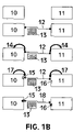
- step 1 of the flow chart of FIG. 1 a the generics of two instances 10 and 11 are located on the chip. The connection between these instances 10 and 11 is not yet routed.
- an initial route 12 is generated between said instances 10 and 11 by a wiring tool. Therefore, the route between the corresponding generics is optimized according to the following design rules.
- the minimum/maximum width and spacing of wires has to be considered.
- the length of the initial route should be as short as possible.
- the position of the initial route should be available in one, here predetermined layer.
- the layer for wiring can be determined e.g. to optimize the performance of the net generated. As in this layer a blockage 13 is located between the instances 10 and 11 , a straight connection between the instances 10 and 11 is not possible.
- the initial route 12 detours the blockade 13 .
- the layout generator creates the layout for each of the instances 10 and 11 in place of the corresponding generics by considering the corresponding optimized pin location.
- the pin 15 could be created at the desired location.
- the desired pin location was not available. Pin 16 had to be created a little bit displaced to this desired location. The rest of the layout of the instances 10 and 11 is created and aligned as is state of the art.
- step 4 the layout generator returns the actual pin locations that were available to the wiring tool, what is indicated by the arrows 17 .
- step 5 the wiring tool does the final route 18 to the actual pin locations which means connecting the actually generated pins 15 and 16 with the corresponding ends of the initial route 12 .
- the driver of the so generated net can automatically be adapted to the chosen wiring solution.
Landscapes
- Engineering & Computer Science (AREA)
- Computer Hardware Design (AREA)
- Physics & Mathematics (AREA)
- Theoretical Computer Science (AREA)
- Computer Networks & Wireless Communication (AREA)
- Evolutionary Computation (AREA)
- Geometry (AREA)
- General Engineering & Computer Science (AREA)
- General Physics & Mathematics (AREA)
- Design And Manufacture Of Integrated Circuits (AREA)
- Semiconductor Integrated Circuits (AREA)
Abstract
Description
-
- minimum/maximum width and spacing of wires;
- the length of the initial route should be as short as possible,
- the position of the initial route should be available in one layer,
- the initial route is positioned in a predetermined layer. In this context it should be mentioned that it is also possible to consider less, more or different design rules by generating an initial route without leaving the scope of protection of the claimed invention.
Claims (7)
Priority Applications (1)
| Application Number | Priority Date | Filing Date | Title |
|---|---|---|---|
| US12/099,998 US20080301616A1 (en) | 2003-12-11 | 2008-04-09 | Layout Generator for Routing and Designing an LSI |
Applications Claiming Priority (3)
| Application Number | Priority Date | Filing Date | Title |
|---|---|---|---|
| EP03104166 | 2003-12-11 | ||
| EP03104166.8 | 2003-12-11 | ||
| EP03104166 | 2003-12-11 |
Related Child Applications (1)
| Application Number | Title | Priority Date | Filing Date |
|---|---|---|---|
| US12/099,998 Division US20080301616A1 (en) | 2003-12-11 | 2008-04-09 | Layout Generator for Routing and Designing an LSI |
Publications (2)
| Publication Number | Publication Date |
|---|---|
| US20050132319A1 US20050132319A1 (en) | 2005-06-16 |
| US7401312B2 true US7401312B2 (en) | 2008-07-15 |
Family
ID=34639305
Family Applications (2)
| Application Number | Title | Priority Date | Filing Date |
|---|---|---|---|
| US10/983,819 Expired - Fee Related US7401312B2 (en) | 2003-12-11 | 2004-11-08 | Automatic method for routing and designing an LSI |
| US12/099,998 Abandoned US20080301616A1 (en) | 2003-12-11 | 2008-04-09 | Layout Generator for Routing and Designing an LSI |
Family Applications After (1)
| Application Number | Title | Priority Date | Filing Date |
|---|---|---|---|
| US12/099,998 Abandoned US20080301616A1 (en) | 2003-12-11 | 2008-04-09 | Layout Generator for Routing and Designing an LSI |
Country Status (1)
| Country | Link |
|---|---|
| US (2) | US7401312B2 (en) |
Cited By (2)
| Publication number | Priority date | Publication date | Assignee | Title |
|---|---|---|---|---|
| US10216890B2 (en) | 2004-04-21 | 2019-02-26 | Iym Technologies Llc | Integrated circuits having in-situ constraints |
| US10248752B2 (en) | 2016-01-11 | 2019-04-02 | Samsung Electronics Co., Ltd. | Method for routing between pins of semiconductor device and design system therewith |
Families Citing this family (4)
| Publication number | Priority date | Publication date | Assignee | Title |
|---|---|---|---|---|
| CA2688716A1 (en) * | 2007-05-16 | 2008-11-27 | Plant Equipment, Inc. | Systems and methods for validating power integrity of integrated circuits |
| JP5309835B2 (en) * | 2008-09-24 | 2013-10-09 | 富士通株式会社 | Wiring information generation apparatus, method, and program |
| US8555232B2 (en) * | 2011-02-28 | 2013-10-08 | Apple Inc. | Wire routing using virtual landing pads |
| CN111199133B (en) * | 2019-12-27 | 2023-09-15 | 成都锐成芯微科技股份有限公司 | Automatic wiring and winding method |
Citations (8)
| Publication number | Priority date | Publication date | Assignee | Title |
|---|---|---|---|---|
| US4831543A (en) * | 1986-02-21 | 1989-05-16 | Harris Semiconductor (Patents) Inc. | Hierarchical net list derivation system |
| US6324675B1 (en) * | 1998-12-18 | 2001-11-27 | Synopsys, Inc. | Efficient iterative, gridless, cost-based fine router for computer controlled integrated circuit design |
| US6330707B1 (en) | 1997-09-29 | 2001-12-11 | Matsushita Electric Industrial Co., Ltd. | Automatic routing method |
| US6349403B1 (en) * | 1998-12-18 | 2002-02-19 | Synopsys, Inc. | Interative, gridless, cost-based layer assignment coarse router for computer controlled IC design |
| US6415426B1 (en) * | 2000-06-02 | 2002-07-02 | Incentia Design Systems, Inc. | Dynamic weighting and/or target zone analysis in timing driven placement of cells of an integrated circuit design |
| US20030088843A1 (en) * | 2001-11-02 | 2003-05-08 | Sun Microsystems, Inc. | Data structure for fine-grid multi-level vlsi routing and method for storing the data structure in a computer readable medium |
| US20030188268A1 (en) * | 2002-03-15 | 2003-10-02 | Sun Microsystems, Inc. | Low Vt transistor substitution in a semiconductor device |
| US6668360B1 (en) * | 2001-01-08 | 2003-12-23 | Taiwan Semiconductor Manufacturing Company | Automatic integrated circuit design kit qualification service provided through the internet |
Family Cites Families (14)
| Publication number | Priority date | Publication date | Assignee | Title |
|---|---|---|---|---|
| US5638293A (en) * | 1994-09-13 | 1997-06-10 | Lsi Logic Corporation | Optimal pad location method for microelectronic circuit cell placement |
| US5757658A (en) * | 1996-03-06 | 1998-05-26 | Silicon Graphics, Inc. | Procedure and system for placement optimization of cells within circuit blocks by optimizing placement of input/output ports within an integrated circuit design |
| US6336207B2 (en) * | 1997-05-27 | 2002-01-01 | Matsushita Electric Industrial Co., Ltd. | Method and apparatus for designing LSI layout, cell library for designing LSI layout and semiconductor integrated circuit |
| JP4090118B2 (en) * | 1998-06-19 | 2008-05-28 | 富士通株式会社 | LSI manufacturing method and recording medium recording layout program |
| US6330708B1 (en) * | 1998-09-17 | 2001-12-11 | International Business Machines Corporation | Method for preparing command files for photomask production |
| US6298468B1 (en) * | 1999-05-04 | 2001-10-02 | Prosper Design Systems Pte. Ltd. | Placement-based pin optimization method and apparatus for computer-aided circuit design |
| JP3988330B2 (en) * | 1999-08-04 | 2007-10-10 | 富士通株式会社 | Semiconductor design system and recording medium recording semiconductor design program |
| US6460169B1 (en) * | 1999-10-21 | 2002-10-01 | International Business Machines Corporation | Routing program method for positioning unit pins in a hierarchically designed VLSI chip |
| US6966045B2 (en) * | 1999-12-27 | 2005-11-15 | Kabushiki Kaisha Toshiba | Method and computer program product for estimating wire loads |
| JP2001298091A (en) * | 2000-04-17 | 2001-10-26 | Mitsubishi Electric Corp | Technique of automatically arranged wiring and semiconductor integrated circuit |
| US6567967B2 (en) * | 2000-09-06 | 2003-05-20 | Monterey Design Systems, Inc. | Method for designing large standard-cell base integrated circuits |
| JP2003085222A (en) * | 2001-09-06 | 2003-03-20 | Mitsubishi Electric Corp | Automatic arranging/wiring device and method and its program |
| US6701505B1 (en) * | 2001-11-30 | 2004-03-02 | Sequence Design, Inc. | Circuit optimization for minimum path timing violations |
| US20050076319A1 (en) * | 2003-10-03 | 2005-04-07 | Chow Shau-Lim Stan | Pin assignment in block-based integrated circuit design methodologies |
-
2004
- 2004-11-08 US US10/983,819 patent/US7401312B2/en not_active Expired - Fee Related
-
2008
- 2008-04-09 US US12/099,998 patent/US20080301616A1/en not_active Abandoned
Patent Citations (8)
| Publication number | Priority date | Publication date | Assignee | Title |
|---|---|---|---|---|
| US4831543A (en) * | 1986-02-21 | 1989-05-16 | Harris Semiconductor (Patents) Inc. | Hierarchical net list derivation system |
| US6330707B1 (en) | 1997-09-29 | 2001-12-11 | Matsushita Electric Industrial Co., Ltd. | Automatic routing method |
| US6324675B1 (en) * | 1998-12-18 | 2001-11-27 | Synopsys, Inc. | Efficient iterative, gridless, cost-based fine router for computer controlled integrated circuit design |
| US6349403B1 (en) * | 1998-12-18 | 2002-02-19 | Synopsys, Inc. | Interative, gridless, cost-based layer assignment coarse router for computer controlled IC design |
| US6415426B1 (en) * | 2000-06-02 | 2002-07-02 | Incentia Design Systems, Inc. | Dynamic weighting and/or target zone analysis in timing driven placement of cells of an integrated circuit design |
| US6668360B1 (en) * | 2001-01-08 | 2003-12-23 | Taiwan Semiconductor Manufacturing Company | Automatic integrated circuit design kit qualification service provided through the internet |
| US20030088843A1 (en) * | 2001-11-02 | 2003-05-08 | Sun Microsystems, Inc. | Data structure for fine-grid multi-level vlsi routing and method for storing the data structure in a computer readable medium |
| US20030188268A1 (en) * | 2002-03-15 | 2003-10-02 | Sun Microsystems, Inc. | Low Vt transistor substitution in a semiconductor device |
Cited By (5)
| Publication number | Priority date | Publication date | Assignee | Title |
|---|---|---|---|---|
| US10216890B2 (en) | 2004-04-21 | 2019-02-26 | Iym Technologies Llc | Integrated circuits having in-situ constraints |
| US10846454B2 (en) | 2004-04-21 | 2020-11-24 | Iym Technologies Llc | Integrated circuits having in-situ constraints |
| US10860773B2 (en) | 2004-04-21 | 2020-12-08 | Iym Technologies Llc | Integrated circuits having in-situ constraints |
| US10248752B2 (en) | 2016-01-11 | 2019-04-02 | Samsung Electronics Co., Ltd. | Method for routing between pins of semiconductor device and design system therewith |
| US10509884B2 (en) | 2016-01-11 | 2019-12-17 | Samsung Electronics Co., Ltd. | Method for routing between pins of semiconductor device and design system therewith |
Also Published As
| Publication number | Publication date |
|---|---|
| US20050132319A1 (en) | 2005-06-16 |
| US20080301616A1 (en) | 2008-12-04 |
Similar Documents
| Publication | Publication Date | Title |
|---|---|---|
| US6415422B1 (en) | Method and system for performing capacitance estimations on an integrated circuit design routed by a global routing tool | |
| US6539529B2 (en) | Method and apparatus for designing integrated circuits and storage medium for storing the method | |
| JP3891599B2 (en) | Device for automatic insertion of standard cells into an integrated circuit layout. | |
| US8788999B1 (en) | Automatic routing system with variable width interconnect | |
| US8479141B1 (en) | Automation using spine routing | |
| US5461576A (en) | Electronic design automation tool for the design of a semiconductor integrated circuit chip | |
| US20080301616A1 (en) | Layout Generator for Routing and Designing an LSI | |
| US20050114821A1 (en) | Distributed autorouting of conductive paths | |
| US6360350B1 (en) | Method and system for performing circuit analysis on an integrated-circuit design having design data available in different forms | |
| US6502229B2 (en) | Method for inserting antenna diodes into an integrated circuit design | |
| Chang et al. | Postlayout logic restructuring using alternative wires | |
| US7069532B2 (en) | Access cell design and a method for enabling automatic insertion of access cells into an integrated circuit design | |
| US6075934A (en) | Method for optimizing contact pin placement in an integrated circuit | |
| CN100382087C (en) | Semiconductor device, semiconductor device wiring method and manufacturing method thereof | |
| US7373628B1 (en) | Method of automatically routing nets using a Steiner tree | |
| US6820048B1 (en) | 4 point derating scheme for propagation delay and setup/hold time computation | |
| US6260184B1 (en) | Design of an integrated circuit by selectively reducing or maintaining power lines of the device | |
| Kheterpal et al. | Routing architecture exploration for regular fabrics | |
| US6654943B2 (en) | Method, system, and computer program product for correcting anticipated problems related to global routing | |
| US6615401B1 (en) | Blocked net buffer insertion | |
| JP2005235804A (en) | Design method and program of semiconductor device | |
| US6477690B1 (en) | In-place repeater insertion methodology for over-the-block routed integrated circuits | |
| JP2008227035A (en) | Cell data for spare cell, design method of semiconductor integrated circuit, and semiconductor integrated circuit | |
| JP4987787B2 (en) | Placement verification device | |
| JP2003281210A (en) | Layout design method and data library providing method |
Legal Events
| Date | Code | Title | Description |
|---|---|---|---|
| AS | Assignment |
Owner name: INTERNATIONAL BUSINESS MACHINES CORPORATION, NEW Y Free format text: ASSIGNMENT OF ASSIGNORS INTEREST;ASSIGNORS:KRAUCH, ULRICH;PILLE, JUERGEN;WERNER, TOBIAS;AND OTHERS;REEL/FRAME:017184/0607;SIGNING DATES FROM 20041025 TO 20051025 |
|
| FEPP | Fee payment procedure |
Free format text: PAYOR NUMBER ASSIGNED (ORIGINAL EVENT CODE: ASPN); ENTITY STATUS OF PATENT OWNER: LARGE ENTITY |
|
| STCF | Information on status: patent grant |
Free format text: PATENTED CASE |
|
| FPAY | Fee payment |
Year of fee payment: 4 |
|
| AS | Assignment |
Owner name: GLOBALFOUNDRIES U.S. 2 LLC, NEW YORK Free format text: ASSIGNMENT OF ASSIGNORS INTEREST;ASSIGNOR:INTERNATIONAL BUSINESS MACHINES CORPORATION;REEL/FRAME:036550/0001 Effective date: 20150629 |
|
| AS | Assignment |
Owner name: GLOBALFOUNDRIES INC., CAYMAN ISLANDS Free format text: ASSIGNMENT OF ASSIGNORS INTEREST;ASSIGNORS:GLOBALFOUNDRIES U.S. 2 LLC;GLOBALFOUNDRIES U.S. INC.;REEL/FRAME:036779/0001 Effective date: 20150910 |
|
| FPAY | Fee payment |
Year of fee payment: 8 |
|
| AS | Assignment |
Owner name: WILMINGTON TRUST, NATIONAL ASSOCIATION, DELAWARE Free format text: SECURITY AGREEMENT;ASSIGNOR:GLOBALFOUNDRIES INC.;REEL/FRAME:049490/0001 Effective date: 20181127 |
|
| FEPP | Fee payment procedure |
Free format text: MAINTENANCE FEE REMINDER MAILED (ORIGINAL EVENT CODE: REM.); ENTITY STATUS OF PATENT OWNER: LARGE ENTITY |
|
| LAPS | Lapse for failure to pay maintenance fees |
Free format text: PATENT EXPIRED FOR FAILURE TO PAY MAINTENANCE FEES (ORIGINAL EVENT CODE: EXP.); ENTITY STATUS OF PATENT OWNER: LARGE ENTITY |
|
| STCH | Information on status: patent discontinuation |
Free format text: PATENT EXPIRED DUE TO NONPAYMENT OF MAINTENANCE FEES UNDER 37 CFR 1.362 |
|
| FP | Lapsed due to failure to pay maintenance fee |
Effective date: 20200715 |
|
| AS | Assignment |
Owner name: GLOBALFOUNDRIES INC., CAYMAN ISLANDS Free format text: RELEASE BY SECURED PARTY;ASSIGNOR:WILMINGTON TRUST, NATIONAL ASSOCIATION;REEL/FRAME:054636/0001 Effective date: 20201117 |
|
| AS | Assignment |
Owner name: GLOBALFOUNDRIES U.S. INC., NEW YORK Free format text: RELEASE BY SECURED PARTY;ASSIGNOR:WILMINGTON TRUST, NATIONAL ASSOCIATION;REEL/FRAME:056987/0001 Effective date: 20201117 |