US7405782B2 - Liquid crystal display device and method fabricating the same - Google Patents
Liquid crystal display device and method fabricating the same Download PDFInfo
- Publication number
- US7405782B2 US7405782B2 US11/439,130 US43913006A US7405782B2 US 7405782 B2 US7405782 B2 US 7405782B2 US 43913006 A US43913006 A US 43913006A US 7405782 B2 US7405782 B2 US 7405782B2
- Authority
- US
- United States
- Prior art keywords
- pixel
- electrode
- liquid crystal
- crystal display
- display device
- Prior art date
- Legal status (The legal status is an assumption and is not a legal conclusion. Google has not performed a legal analysis and makes no representation as to the accuracy of the status listed.)
- Expired - Lifetime, expires
Links
- 239000004973 liquid crystal related substance Substances 0.000 title claims abstract description 33
- 238000000034 method Methods 0.000 title claims description 16
- 238000004519 manufacturing process Methods 0.000 claims description 21
- 239000000758 substrate Substances 0.000 description 63
- 239000010408 film Substances 0.000 description 40
- 229910021417 amorphous silicon Inorganic materials 0.000 description 17
- 238000002161 passivation Methods 0.000 description 10
- 239000011651 chromium Substances 0.000 description 4
- 238000005229 chemical vapour deposition Methods 0.000 description 3
- 238000007796 conventional method Methods 0.000 description 3
- 229910052751 metal Inorganic materials 0.000 description 3
- 239000002184 metal Substances 0.000 description 3
- 238000004544 sputter deposition Methods 0.000 description 3
- 239000010409 thin film Substances 0.000 description 3
- VYZAMTAEIAYCRO-UHFFFAOYSA-N Chromium Chemical compound [Cr] VYZAMTAEIAYCRO-UHFFFAOYSA-N 0.000 description 2
- 229910052782 aluminium Inorganic materials 0.000 description 2
- XAGFODPZIPBFFR-UHFFFAOYSA-N aluminium Chemical compound [Al] XAGFODPZIPBFFR-UHFFFAOYSA-N 0.000 description 2
- 229910052804 chromium Inorganic materials 0.000 description 2
- 239000011521 glass Substances 0.000 description 2
- 238000000206 photolithography Methods 0.000 description 2
- VYPSYNLAJGMNEJ-UHFFFAOYSA-N silicon dioxide Inorganic materials O=[Si]=O VYPSYNLAJGMNEJ-UHFFFAOYSA-N 0.000 description 2
- 229910052581 Si3N4 Inorganic materials 0.000 description 1
- 238000000137 annealing Methods 0.000 description 1
- 230000015572 biosynthetic process Effects 0.000 description 1
- 239000006185 dispersion Substances 0.000 description 1
- 238000005530 etching Methods 0.000 description 1
- 239000011159 matrix material Substances 0.000 description 1
- 238000012986 modification Methods 0.000 description 1
- 230000004048 modification Effects 0.000 description 1
- 238000000059 patterning Methods 0.000 description 1
- 239000004033 plastic Substances 0.000 description 1
- 239000010453 quartz Substances 0.000 description 1
- HQVNEWCFYHHQES-UHFFFAOYSA-N silicon nitride Chemical compound N12[Si]34N5[Si]62N3[Si]51N64 HQVNEWCFYHHQES-UHFFFAOYSA-N 0.000 description 1
- 229910052814 silicon oxide Inorganic materials 0.000 description 1
- 238000002834 transmittance Methods 0.000 description 1
- 239000012780 transparent material Substances 0.000 description 1
Images


Classifications
-
- G—PHYSICS
- G02—OPTICS
- G02F—OPTICAL DEVICES OR ARRANGEMENTS FOR THE CONTROL OF LIGHT BY MODIFICATION OF THE OPTICAL PROPERTIES OF THE MEDIA OF THE ELEMENTS INVOLVED THEREIN; NON-LINEAR OPTICS; FREQUENCY-CHANGING OF LIGHT; OPTICAL LOGIC ELEMENTS; OPTICAL ANALOGUE/DIGITAL CONVERTERS
- G02F1/00—Devices or arrangements for the control of the intensity, colour, phase, polarisation or direction of light arriving from an independent light source, e.g. switching, gating or modulating; Non-linear optics
- G02F1/01—Devices or arrangements for the control of the intensity, colour, phase, polarisation or direction of light arriving from an independent light source, e.g. switching, gating or modulating; Non-linear optics for the control of the intensity, phase, polarisation or colour
- G02F1/13—Devices or arrangements for the control of the intensity, colour, phase, polarisation or direction of light arriving from an independent light source, e.g. switching, gating or modulating; Non-linear optics for the control of the intensity, phase, polarisation or colour based on liquid crystals, e.g. single liquid crystal display cells
- G02F1/133—Constructional arrangements; Operation of liquid crystal cells; Circuit arrangements
- G02F1/136—Liquid crystal cells structurally associated with a semi-conducting layer or substrate, e.g. cells forming part of an integrated circuit
- G02F1/1362—Active matrix addressed cells
-
- G—PHYSICS
- G02—OPTICS
- G02F—OPTICAL DEVICES OR ARRANGEMENTS FOR THE CONTROL OF LIGHT BY MODIFICATION OF THE OPTICAL PROPERTIES OF THE MEDIA OF THE ELEMENTS INVOLVED THEREIN; NON-LINEAR OPTICS; FREQUENCY-CHANGING OF LIGHT; OPTICAL LOGIC ELEMENTS; OPTICAL ANALOGUE/DIGITAL CONVERTERS
- G02F1/00—Devices or arrangements for the control of the intensity, colour, phase, polarisation or direction of light arriving from an independent light source, e.g. switching, gating or modulating; Non-linear optics
- G02F1/01—Devices or arrangements for the control of the intensity, colour, phase, polarisation or direction of light arriving from an independent light source, e.g. switching, gating or modulating; Non-linear optics for the control of the intensity, phase, polarisation or colour
- G02F1/13—Devices or arrangements for the control of the intensity, colour, phase, polarisation or direction of light arriving from an independent light source, e.g. switching, gating or modulating; Non-linear optics for the control of the intensity, phase, polarisation or colour based on liquid crystals, e.g. single liquid crystal display cells
- G02F1/133—Constructional arrangements; Operation of liquid crystal cells; Circuit arrangements
- G02F1/1333—Constructional arrangements; Manufacturing methods
- G02F1/1335—Structural association of cells with optical devices, e.g. polarisers or reflectors
- G02F1/133509—Filters, e.g. light shielding masks
- G02F1/133514—Colour filters
-
- G—PHYSICS
- G02—OPTICS
- G02F—OPTICAL DEVICES OR ARRANGEMENTS FOR THE CONTROL OF LIGHT BY MODIFICATION OF THE OPTICAL PROPERTIES OF THE MEDIA OF THE ELEMENTS INVOLVED THEREIN; NON-LINEAR OPTICS; FREQUENCY-CHANGING OF LIGHT; OPTICAL LOGIC ELEMENTS; OPTICAL ANALOGUE/DIGITAL CONVERTERS
- G02F1/00—Devices or arrangements for the control of the intensity, colour, phase, polarisation or direction of light arriving from an independent light source, e.g. switching, gating or modulating; Non-linear optics
- G02F1/01—Devices or arrangements for the control of the intensity, colour, phase, polarisation or direction of light arriving from an independent light source, e.g. switching, gating or modulating; Non-linear optics for the control of the intensity, phase, polarisation or colour
- G02F1/13—Devices or arrangements for the control of the intensity, colour, phase, polarisation or direction of light arriving from an independent light source, e.g. switching, gating or modulating; Non-linear optics for the control of the intensity, phase, polarisation or colour based on liquid crystals, e.g. single liquid crystal display cells
- G02F1/133—Constructional arrangements; Operation of liquid crystal cells; Circuit arrangements
- G02F1/136—Liquid crystal cells structurally associated with a semi-conducting layer or substrate, e.g. cells forming part of an integrated circuit
- G02F1/1362—Active matrix addressed cells
- G02F1/13625—Patterning using multi-mask exposure
Definitions
- the invention relates to a liquid crystal display device and a method of fabricating the same, and more particularly to an active matrix type liquid crystal display device and a method of fabricating the same.
- step of forming a pixel electrode and an electrode located in facing relation to the pixel electrode in a process of fabricating a liquid crystal display device in particular, an in plane switching type liquid crystal display device
- stepper projection alignment in which a substrate on which a thin film transistor (TFT) is to be fabricated is divided into a plurality of areas, and each of areas is exposed to light in turn by means of a stepper.
- TFT thin film transistor
- stepper projection alignment a difference is made in a line width and registration among layers because of dispersion in a luminance of light to which divided areas of a substrate is exposed, and/or a difference in light-exposure in areas between which a stitch is located. As a result, differences in capacitance are made among electrodes formed on the TFT substrate.
- stepper projection alignment it is important in stepper projection alignment to reduce non-uniformity in a luminance, caused by the differences in capacitance among electrodes formed on the TFT substrate.
- Japanese Patent Application Publication No. 2000-162639 has suggested a method of fabricating a liquid crystal display device, including a step of forming a pixel electrode and an electrode located in facing relation to the pixel electrode by stepper projection alignment, in which step, the divided areas located adjacent to each other are designed to have an area overlapping each other, and patterns in the divided areas are arranged in random number sequence in the overlapping area.
- an average capacitance of a pixel electrode and an opposing electrode in the overlapping area is just a half of capacitances of the electrodes in the adjacent divided areas. This ensures that a luminance smoothly changes over the adjacent divided areas between which the overlapping area exists, and hence, image-display quality is enhanced.
- Japanese Patent Application Publication No. 11-249169 has suggested a liquid crystal display device including a substrate and at least two pixels arranged on the substrate and allowing a light to pass therethrough at different transmittance.
- Japanese Patent Application Publication No. 2002-182242 has suggested a method of fabricating a liquid crystal display device, including the steps of dividing at least one of an electrically conductive layer and a dielectric layer to a plurality of areas, and exposing each of the divided areas to light to pattern each of the divided areas such that adjacent divided areas have a zigzag stitch therebetween.
- Japanese Patent Application Publication No. 2002-107758 has suggested a method of fabricating a liquid crystal display device, including the steps of dividing a substrate into a plurality of areas, and exposing each of the areas to light by means of a stepper such that two areas located adjacent to each other have an overlapping area which is exposed to light twice. Such an overlapping area is non-linearly formed in a sub-pixel area.
- Japanese Patent Application Publication No. 2000-29053 has suggested a method of fabricating a liquid crystal display device, including the step of repeatedly using a mask for exposing each of pixel areas to light.
- a liquid crystal display device including a display screen comprised of a plurality of areas in each of which a pixel pattern is formed, wherein any two areas located adjacent to each other, among the areas, have at least two stitches therebetween.
- the stitches are located differently from one another for each of pixel rows constituting the display screen.
- the stitches are located differently from one another for each of pixel rows of color pixels constituting a unit pixel.
- a method of fabricating a liquid crystal display device including a step of forming a pixel pattern in each of areas constituting a display screen, by stepping projection alignment, the pixel pattern being formed in each of the areas for each of pixel rows by at least twice carrying out exposure of each of the areas to light such that stitches formed in the exposure between the areas are located differently from one another for the each of pixel rows.
- the pixel rows are comprised of a pixel row of first color pixels, a pixel row of second color pixels, and a pixel row of third color pixels, the first, second and third color pixels defining a unit pixel.
- a reticle having a certain pixel pattern is commonly used for carrying out exposure of each of the areas to light for each of the pixel rows, and a relative position between the reticle and a substrate is made different in exposure of the each of the areas to light for each of the pixel rows.
- a liquid crystal display fabricated in accordance with the present invention would have enhanced quality in displaying images.
- FIG. 1 is a perspective view of a liquid crystal display device in accordance with a first embodiment of the present invention.
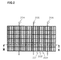
- FIG. 2 is a plan view of a TFT array substrate in the liquid crystal display device in accordance with the first embodiment.
- FIG. 3A is a cross-sectional view taken along the line III-III in FIG. 2 , showing one of steps of a process of fabrication of the TFT array substrate in the liquid crystal display device in accordance with the first embodiment.
- FIG. 3B is a cross-sectional view taken along the line III-III in FIG. 2 , showing one of steps of a process of fabrication of the TFT array substrate in the liquid crystal display device in accordance with the first embodiment.
- FIG. 3C is a cross-sectional view taken along the line III-III in FIG. 2 , showing one of steps of a process of fabrication of the TFT array substrate in the liquid crystal display device in accordance with the first embodiment.
- FIGS. 4A , 4 B and 4 C are plan views of pixel rows to explain stepper projection alignment in the first embodiment.
- FIG. 5 is a plan view of a reticle used in stepper projection alignment in the first embodiment.
- FIG. 6 is a graph showing exposure of a substrate to light in the conventional stepper projection alignment.
- FIG. 7 is a graph showing exposure of a substrate to light in the stepper projection alignment in the first embodiment.
- FIG. 8 is a graph showing a luminance in a unit pixel in the liquid crystal display device in accordance with the first embodiment.
- FIG. 9A is a cross-sectional view of a liquid crystal display device in accordance with the second embodiment, showing one of steps of a process of fabrication of the TFT array substrate in the second embodiment.
- FIG. 9B is a cross-sectional view of a liquid crystal display device in accordance with the second embodiment, showing one of steps of a process of fabrication of the TFT array substrate in the second embodiment.
- FIG. 9C is a cross-sectional view of a liquid crystal display device in accordance with the second embodiment, showing one of steps of a process of fabrication of the TFT array substrate in the second embodiment.
- FIG. 9D is a cross-sectional view of a liquid crystal display device in accordance with the second embodiment, showing one of steps of a process of fabrication of the TFT array substrate in the second embodiment.
- FIGS. 10A , 10 B, 10 C and 10 D are plan views of pixel rows to explain stepper projection alignment in the second embodiment.
- FIG. 1 is a perspective view of a liquid crystal display device in accordance with the first embodiment of the present invention.
- the liquid crystal display device in accordance with the first embodiment is of an in-plane switching (IPS) type.
- IPS in-plane switching
- the liquid crystal display device is comprised of a TFT array substrate 101 on which thin film transistors (TFTs) are fabricated in array, and a color filter substrate 102 located in facing relation to the TFT array substrate 101 with a predetermined gap therebetween.
- TFTs thin film transistors
- FIG. 2 is a plan view of the TFT array substrate 101 in the first embodiment.
- red (R) pixel rows 201 On the TFT array substrate 101 are arranged lines of red (R) pixel rows 201 , lines of green (G) pixel rows 202 , and lines of blue (B) pixel rows 203 .
- R red
- G green
- B blue
- a red pixel, a green pixel and a blue pixel located adjacent to one another cooperate to one another to define a unit pixel.
- FIG. 3C is a cross-sectional view of the TFT array substrate 101 , taken along the line III-III in FIG. 2 .
- the TFT array substrate 101 is comprised of an electrically insulating transparent substrate 301 , a gate electrode 302 formed on the substrate 301 , an electrode 307 facing a pixel (hereinbelow, referred to as “pixel-facing electrode”) and formed on the substrate 301 , an electrically insulating inorganic film 308 formed on the substrate 301 , covering the gate electrode 302 and the pixel-facing electrode 307 therewith, an amorphous silicon layer 303 formed on the electrically insulating inorganic film 308 above the gate electrode 302 , a drain electrode 304 formed on the electrically insulating inorganic film 308 and partially covering the amorphous silicon layer 303 therewith, a source electrode 305 formed on the electrically insulating inorganic film 308 and partially covering the amorphous silicon layer 303 therewith, a pixel electrode 306 formed on the electrically insulating inorganic film 308 , and a passivation film 309 covering the amorph
- the gate electrode 302 , the amorphous silicon layer 303 , the drain electrode 304 and the source electrode 305 constitute a thin film transistor (TFT).
- TFT thin film transistor
- the drain electrode 304 and the pixel electrode 306 are formed in a common layer
- the gate electrode 302 and the pixel-facing electrode 307 are formed in a common layer
- the pixel electrode 306 and the pixel-facing electrode 307 are formed in different layers.
- FIGS. 3A to 3C are cross-sectional views taken along the line III-III in FIG. 2 , each showing one of steps of a process of fabrication of the TFT array substrate 101 .
- a process of fabricating the TFT array substrate 101 is explained with reference to FIGS. 3A to 3C .
- the gate electrode 302 and the pixel-facing electrode 307 are formed on the substrate 301 .
- the substrate 301 is composed of transparent material which is not deformed and denaturalized in annealing.
- the substrate 301 is composed of glass, quartz or plastic.
- the substrate 301 is composed of glass.
- the gate electrode 302 and the pixel-facing electrode 307 are comprised of a metal film such as a chromium (Cr) or aluminum (Al) film, and formed by sputtering, for instance.
- a metal film such as a chromium (Cr) or aluminum (Al) film, and formed by sputtering, for instance.
- the electrically insulating inorganic film 308 is formed on the substrate 301 such that the gate electrode 302 and the pixel-facing electrode 307 are entirely covered with the electrically insulating inorganic film 308 .
- an amorphous silicon film is formed on the electrically insulating inorganic film 308 by chemical vapor deposition (CVD), for instance. Then, the amorphous silicon film is patterned by photolithography and etching into the amorphous silicon layer 303 , as illustrated in FIG. 3B .
- CVD chemical vapor deposition
- the drain electrode 304 and the source electrode 305 are formed on the electrically insulating inorganic film 308 such that they partially cover the amorphous silicon layer 303 .
- the pixel electrode 306 is formed on the electrically insulating inorganic film 308 . That is, are formed in a common layer.
- the drain electrode 304 , the source electrode 305 and the pixel electrode 306 are comprised of a metal film such as a chromium (Cr) or aluminum (Al) film, and formed by sputtering, for instance.
- a metal film such as a chromium (Cr) or aluminum (Al) film, and formed by sputtering, for instance.
- the passivation film 309 comprised of a silicon oxide film or a silicon nitride film is formed entirely over the electrically insulating inorganic film 308 , the drain electrode 304 , the amorphous silicon layer 303 , the source electrode 305 and the pixel electrode 306 by sputtering or CVD.
- the TFT array substrate 101 is completed.
- the gate electrode 302 , the pixel-facing electrode 307 , the amorphous silicon film 303 , the drain electrode 304 , the source electrode 305 and the pixel electrode 306 are all patterned by photolithography.
- the step of exposing them to light, which is a most important step in patterning them, is carried out as stepper projection alignment which is usually used in fabrication of middle and large-sized panels of five-inches or more size.
- stepper projection alignment is carried out for each of color pixels by shifting a stitch.
- stepper projection alignment is carried out at a first stitch position 204 for the red pixel rows 201 , at a second stitch position 205 for the green pixel rows 202 , and at a third stitch position 206 for the blue pixel rows 203 .
- an upper half indicates a location of a reticle
- a lower half indicates a pixel pattern of the TFT array substrate 101 in association with each of patterns of the reticle.
- the TFT array substrate 101 is exposed to light with one stitch 151 , as illustrated in FIG. 4A .
- stepper projection alignment is carried out three times in an area. Specifically, stepper projection alignment is carried out at the stitch 151 for exposure of red pixels, then, at two stitches 152 a and 152 b (see FIG. 4B ) for exposure of green pixels, and finally, at two stitches 153 a and 153 b (see FIG. 4C ) for exposure of blue pixels.
- the stitches are located different from one another for each of red, green and blue color pixels, as illustrated in FIGS. 4A , 4 B and 4 C.
- FIG. 5 is a plan view illustrating an example of the reticle.
- the reticle is designed to have a common pattern 501 for each of red, green and blue color pixels.
- the stitches are located different from one another for each of red, green and blue color pixels by shifting an exposure area in the first embodiment, unlike the conventional stepper projection alignment in which the TFT array substrate is divided into unit pixel areas.
- the first embodiment provides an advantage that a difference in a capacitance and an aperture ratio can be reduced which difference is caused by a difference in a line width and/or registration of a layer between adjacent areas between which a stitch exists.
- FIG. 6 shows a relation between exposure and a location of a TFT array substrate in the conventional stepper projection alignment.
- a stitch remains in the same position for each of red, green and blue pixels when a substrate is exposed to light, and resultingly, exposure remarkably increases at the stitch 601 .
- FIG. 7 shows a relation between exposure and a location of the TFT array substrate 101 in the first embodiment.
- a first stitch 701 for exposure of the TFT array substrate 101 to light for red pixels, a second stitch 702 for exposure of the TFT array substrate 101 to light for green pixels, and a third stitch 703 for exposure of the TFT array substrate 101 to light for blue pixels are located differently from one another, as illustrated in FIG. 7 .
- a luminance in a panel would have a profile in accordance with the exposure profile.
- a luminance profile in a panel in a unit pixel is such a profile as illustrated in FIG. 8 .
- a luminance varies at a stitch only in any one of red, green and blue pixels with respect to a unit pixel comprised of red, green and blue pixels.
- a luminance difference across a stitch is about one-third (1 ⁇ 3). That is, the first embodiment can reduce a luminance difference between adjacent divided areas to a greater degree than the conventional method.
- FIG. 9D is a cross-sectional view of a TFT array substrate in a liquid crystal display device in accordance with the second embodiment.
- the TFT array substrate 101 A is comprised of an electrically insulating transparent substrate 901 , a gate electrode 902 formed on the substrate 901 , an electrically insulating inorganic film 903 formed on the substrate 301 , covering the gate electrode 902 therewith, an amorphous silicon layer 904 formed on the electrically insulating inorganic film 903 above the gate electrode 902 , a drain electrode 905 formed on the electrically insulating inorganic film 903 and partially covering the amorphous silicon layer 904 therewith, a source electrode 906 formed on the electrically insulating inorganic film 903 and partially covering the amorphous silicon layer 904 therewith, a passivation film 907 covering the amorphous silicon layer 904 , the drain electrode 905 , the source electrode 906 and the electrically insulating inorganic film 903 therewith, a pixel electrode 910 formed on the passivation film 907 and making electrical contact with the source electrode 906 through a contact hole
- the pixel electrode 910 and the pixel-facing electrode 911 are concurrently formed on the passivation film 907 .
- the present invention may be applied to the step of concurrently forming the pixel electrode 910 and the pixel-facing electrode 911 .
- FIGS. 9A to 9D are cross-sectional of the TFT array substrate 101 A, each showing one of steps of a process of fabrication of the TFT array substrate 101 A.
- a process of fabricating the TFT array substrate 101 A is explained with reference to FIGS. 9A to 9D .
- the gate electrode 902 is formed on the substrate 901 .
- the electrically insulating inorganic film 903 is formed on the substrate 901 such that the gate electrode 902 is entirely covered with the electrically insulating inorganic film 903 .
- the amorphous silicon layer 904 is formed on the electrically insulating inorganic film 903 above the gate electrode 902 , as illustrated in FIG. 9B .
- the drain electrode 905 and the source electrode 906 are formed on the electrically insulating inorganic film 903 such that they partially cover the amorphous silicon film 904 therewith.
- the passivation film 907 is formed entirely over the substrate 901 , as illustrated in FIG. 9C .
- contact holes 908 A and 908 B are formed throughout the passivation film 907 in alignment with the source electrode 906 and the gate electrode 902 , as illustrated in FIG. 9C .
- the pixel electrode 910 is formed on the passivation film 907 and making electrical contact with the source electrode 906 through the contact hole 908 A, and concurrently, the pixel-facing electrode 911 is formed on the passivation film 907 and making electrical contact with the gate electrode 902 through the contact hole 908 B, as illustrated in FIG. 9D .
- the TFT array substrate 101 A in the second embodiment is completed.
- a step of exposing the substrate to light is carried out three times for each of red, green and blue pixels in a divided area.
- a step of exposing the substrate to light may be carried out four or more times.
- an upper half indicates a location of a reticle
- a lower half indicates a pixel pattern of the TFT array substrate 101 A in association with each of patterns of the reticle.
- stepper projection alignment is carried out at a stitch 161 for exposure of the pixel rows A, as illustrated in FIG. 10A .
- stepper projection alignment is carried out at a stitch 162 for exposure of the pixel rows B, as illustrated in FIG. 10B .
- stepper projection alignment is carried out at a stitch 163 for exposure of the pixel rows C, as illustrated in FIG. 10C .
- stepper projection alignment is carried out at a stitch 164 for exposure of the pixel rows D, as illustrated in FIG. 10D .
- the four stitches 161 to 164 are located different from one another for each of the pixel rows A to D, as illustrated in FIGS. 10A to 10D .
- FIG. 5 is a plan view illustrating an example of the reticle.
Abstract
Description
Claims (3)
Priority Applications (1)
| Application Number | Priority Date | Filing Date | Title |
|---|---|---|---|
| US11/439,130 US7405782B2 (en) | 2002-11-19 | 2006-05-24 | Liquid crystal display device and method fabricating the same |
Applications Claiming Priority (5)
| Application Number | Priority Date | Filing Date | Title |
|---|---|---|---|
| JP2002335264A JP4328515B2 (en) | 2002-11-19 | 2002-11-19 | Liquid crystal display device and manufacturing method thereof |
| JP2002-335264 | 2002-11-19 | ||
| US10/715,529 US7136120B2 (en) | 2002-11-19 | 2003-11-19 | Liquid crystal display device and method of fabricating the same |
| US11/192,122 US7151587B2 (en) | 2002-11-19 | 2005-07-29 | Liquid crystal display device and method of fabricating the same |
| US11/439,130 US7405782B2 (en) | 2002-11-19 | 2006-05-24 | Liquid crystal display device and method fabricating the same |
Related Parent Applications (1)
| Application Number | Title | Priority Date | Filing Date |
|---|---|---|---|
| US11/192,122 Division US7151587B2 (en) | 2002-11-19 | 2005-07-29 | Liquid crystal display device and method of fabricating the same |
Publications (2)
| Publication Number | Publication Date |
|---|---|
| US20060209249A1 US20060209249A1 (en) | 2006-09-21 |
| US7405782B2 true US7405782B2 (en) | 2008-07-29 |
Family
ID=32321759
Family Applications (4)
| Application Number | Title | Priority Date | Filing Date |
|---|---|---|---|
| US10/715,529 Active 2024-04-28 US7136120B2 (en) | 2002-11-19 | 2003-11-19 | Liquid crystal display device and method of fabricating the same |
| US11/192,122 Expired - Lifetime US7151587B2 (en) | 2002-11-19 | 2005-07-29 | Liquid crystal display device and method of fabricating the same |
| US11/439,130 Expired - Lifetime US7405782B2 (en) | 2002-11-19 | 2006-05-24 | Liquid crystal display device and method fabricating the same |
| US11/439,131 Expired - Lifetime US7388644B2 (en) | 2002-11-19 | 2006-05-24 | Liquid crystal display device and method of fabricating the same |
Family Applications Before (2)
| Application Number | Title | Priority Date | Filing Date |
|---|---|---|---|
| US10/715,529 Active 2024-04-28 US7136120B2 (en) | 2002-11-19 | 2003-11-19 | Liquid crystal display device and method of fabricating the same |
| US11/192,122 Expired - Lifetime US7151587B2 (en) | 2002-11-19 | 2005-07-29 | Liquid crystal display device and method of fabricating the same |
Family Applications After (1)
| Application Number | Title | Priority Date | Filing Date |
|---|---|---|---|
| US11/439,131 Expired - Lifetime US7388644B2 (en) | 2002-11-19 | 2006-05-24 | Liquid crystal display device and method of fabricating the same |
Country Status (2)
| Country | Link |
|---|---|
| US (4) | US7136120B2 (en) |
| JP (1) | JP4328515B2 (en) |
Cited By (1)
| Publication number | Priority date | Publication date | Assignee | Title |
|---|---|---|---|---|
| US8669550B2 (en) | 2005-09-29 | 2014-03-11 | Semiconductor Energy Laboratory Co., Ltd. | Semiconductor device and manufacturing method thereof |
Families Citing this family (1)
| Publication number | Priority date | Publication date | Assignee | Title |
|---|---|---|---|---|
| KR102544324B1 (en) * | 2018-01-16 | 2023-06-19 | 삼성디스플레이 주식회사 | Mask, and exposure method of display using therof |
Citations (10)
| Publication number | Priority date | Publication date | Assignee | Title |
|---|---|---|---|---|
| US5945256A (en) | 1997-12-06 | 1999-08-31 | Samsung Electronics Co., Ltd. | Exposing methods in photolithography used for manufacturing a liquid crystal display |
| JPH11249169A (en) | 1998-03-04 | 1999-09-17 | Mitsubishi Electric Corp | Liquid crystal display device and manufacture thereof |
| JP2000029053A (en) | 1998-07-14 | 2000-01-28 | Mitsubishi Electric Corp | Liquid crystal display device and is manufacture |
| JP2000162639A (en) | 1998-11-26 | 2000-06-16 | Advanced Display Inc | Liquid crystal display device and its production |
| US6146796A (en) | 1997-12-01 | 2000-11-14 | Samsung Electronics Co., Ltd. | Liquid crystal display and a manufacturing method thereof |
| US6356320B1 (en) | 1999-11-03 | 2002-03-12 | Lg. Philips Lcd Co., Ltd. | LCD with TFT array having wave-shaped resistance pattern to correct stitching defect |
| JP2002107758A (en) | 2000-09-21 | 2002-04-10 | Internatl Business Mach Corp <Ibm> | Method for manufacturing liquid crystal display device, method for manufacturing display device and liquid crystal display device |
| JP2002182242A (en) | 2000-12-14 | 2002-06-26 | Toshiba Corp | Method for producing liquid crystal display |
| US20040119927A1 (en) * | 2002-12-18 | 2004-06-24 | Kang Dong Ho | In-plane switching mode liquid crystal display device |
| US20040207798A1 (en) | 2001-12-14 | 2004-10-21 | Young-Mi Tak | Manufacturing method of a panel for liquid crystal |
-
2002
- 2002-11-19 JP JP2002335264A patent/JP4328515B2/en not_active Expired - Lifetime
-
2003
- 2003-11-19 US US10/715,529 patent/US7136120B2/en active Active
-
2005
- 2005-07-29 US US11/192,122 patent/US7151587B2/en not_active Expired - Lifetime
-
2006
- 2006-05-24 US US11/439,130 patent/US7405782B2/en not_active Expired - Lifetime
- 2006-05-24 US US11/439,131 patent/US7388644B2/en not_active Expired - Lifetime
Patent Citations (10)
| Publication number | Priority date | Publication date | Assignee | Title |
|---|---|---|---|---|
| US6146796A (en) | 1997-12-01 | 2000-11-14 | Samsung Electronics Co., Ltd. | Liquid crystal display and a manufacturing method thereof |
| US5945256A (en) | 1997-12-06 | 1999-08-31 | Samsung Electronics Co., Ltd. | Exposing methods in photolithography used for manufacturing a liquid crystal display |
| JPH11249169A (en) | 1998-03-04 | 1999-09-17 | Mitsubishi Electric Corp | Liquid crystal display device and manufacture thereof |
| JP2000029053A (en) | 1998-07-14 | 2000-01-28 | Mitsubishi Electric Corp | Liquid crystal display device and is manufacture |
| JP2000162639A (en) | 1998-11-26 | 2000-06-16 | Advanced Display Inc | Liquid crystal display device and its production |
| US6356320B1 (en) | 1999-11-03 | 2002-03-12 | Lg. Philips Lcd Co., Ltd. | LCD with TFT array having wave-shaped resistance pattern to correct stitching defect |
| JP2002107758A (en) | 2000-09-21 | 2002-04-10 | Internatl Business Mach Corp <Ibm> | Method for manufacturing liquid crystal display device, method for manufacturing display device and liquid crystal display device |
| JP2002182242A (en) | 2000-12-14 | 2002-06-26 | Toshiba Corp | Method for producing liquid crystal display |
| US20040207798A1 (en) | 2001-12-14 | 2004-10-21 | Young-Mi Tak | Manufacturing method of a panel for liquid crystal |
| US20040119927A1 (en) * | 2002-12-18 | 2004-06-24 | Kang Dong Ho | In-plane switching mode liquid crystal display device |
Cited By (5)
| Publication number | Priority date | Publication date | Assignee | Title |
|---|---|---|---|---|
| US8669550B2 (en) | 2005-09-29 | 2014-03-11 | Semiconductor Energy Laboratory Co., Ltd. | Semiconductor device and manufacturing method thereof |
| US8790959B2 (en) | 2005-09-29 | 2014-07-29 | Semiconductor Energy Laboratory Co., Ltd. | Semiconductor device and manufacturing method thereof |
| US8796069B2 (en) | 2005-09-29 | 2014-08-05 | Semiconductor Energy Laboratory Co., Ltd. | Semiconductor device and manufacturing method thereof |
| US9099562B2 (en) | 2005-09-29 | 2015-08-04 | Semiconductor Energy Laboratory Co., Ltd. | Semiconductor device and manufacturing method thereof |
| US10304962B2 (en) | 2005-09-29 | 2019-05-28 | Semiconductor Energy Laboratory Co., Ltd. | Semiconductor device and manufacturing method thereof |
Also Published As
| Publication number | Publication date |
|---|---|
| US20050264745A1 (en) | 2005-12-01 |
| US20040100605A1 (en) | 2004-05-27 |
| US7136120B2 (en) | 2006-11-14 |
| JP2004170620A (en) | 2004-06-17 |
| US20060209234A1 (en) | 2006-09-21 |
| US7151587B2 (en) | 2006-12-19 |
| JP4328515B2 (en) | 2009-09-09 |
| US7388644B2 (en) | 2008-06-17 |
| US20060209249A1 (en) | 2006-09-21 |
Similar Documents
| Publication | Publication Date | Title |
|---|---|---|
| US7742130B2 (en) | Color filter plate and thin film transistor plate for liquid crystal display, and methods for fabricating the plates | |
| USRE43574E1 (en) | Four color liquid crystal display and panel therefor | |
| US7859629B2 (en) | In-plane switching mode liquid crystal display wherein the upper and lower pixel electrodes are arranged on opposite sides of the respective upper and lower pixel regions | |
| US7196761B2 (en) | LCD array substrate and fabrication method thereof | |
| JP4401551B2 (en) | Method for manufacturing liquid crystal display device, method for manufacturing display device, and liquid crystal display device | |
| JP2005258408A (en) | In-plane switching mode liquid crystal display and its manufacturing method | |
| US20070052888A1 (en) | Liquid crystal display and manufacturing method thereof | |
| US8466863B2 (en) | Liquid crystal display and method for manufacturing the same | |
| JP4728507B2 (en) | Active matrix liquid crystal display device and manufacturing method thereof | |
| CN1949041B (en) | Method of fabricating liquid crystal display device | |
| KR101483024B1 (en) | Liquid crystal display device and method of fabricating the same | |
| US11073734B2 (en) | Array substrate and method of manufacturing the same, display panel and display device | |
| US20070001961A1 (en) | Method of forming fine pattern, liquid crystal display device having a fine pattern and fabricating method thereof | |
| US7405782B2 (en) | Liquid crystal display device and method fabricating the same | |
| KR101201707B1 (en) | Liquid crystal display device and method of fabricating the same | |
| WO1996038755A1 (en) | Liquid crystal display and production method therefor | |
| US7696027B2 (en) | Method of fabricating display substrate and method of fabricating display panel using the same | |
| KR20170080215A (en) | Liquid crystal image display device | |
| US9910313B2 (en) | Liquid crystal display device and manufacturing method thereof | |
| KR101206286B1 (en) | Method of fabricating liquid crystal display device | |
| KR100992121B1 (en) | Thin film transistor array panel and liquid crystal display including the panel | |
| WO2021128518A1 (en) | Method for manufacturing pattern of thin film transistor, thin film transistor and photomask | |
| US20030123020A1 (en) | Method of dividing an exposing region | |
| KR101266274B1 (en) | Liquid crystal display device and method of fabricating the same | |
| KR20070079217A (en) | Liquid crystal display device and method of fabricating the same |
Legal Events
| Date | Code | Title | Description |
|---|---|---|---|
| AS | Assignment |
Owner name: NEC LCD TECHNOLOGIES, LTD., JAPAN Free format text: ASSIGNMENT OF ASSIGNORS INTEREST;ASSIGNORS:ISHINO, TAKAYUKI;YAMAMOTO, YUJI;NAKATA, SHINICHI;AND OTHERS;REEL/FRAME:017925/0627 Effective date: 20031110 |
|
| STCF | Information on status: patent grant |
Free format text: PATENTED CASE |
|
| AS | Assignment |
Owner name: NEC CORPORATION,JAPAN Free format text: ASSIGNMENT OF ASSIGNORS INTEREST;ASSIGNOR:NEC LCD TECHNOLOGIES, LTD.;REEL/FRAME:024492/0176 Effective date: 20100301 Owner name: NEC CORPORATION, JAPAN Free format text: ASSIGNMENT OF ASSIGNORS INTEREST;ASSIGNOR:NEC LCD TECHNOLOGIES, LTD.;REEL/FRAME:024492/0176 Effective date: 20100301 |
|
| FPAY | Fee payment |
Year of fee payment: 4 |
|
| AS | Assignment |
Owner name: GOLD CHARM LIMITED, SAMOA Free format text: ASSIGNMENT OF ASSIGNORS INTEREST;ASSIGNOR:NEC CORPORATION;REEL/FRAME:029977/0847 Effective date: 20121130 |
|
| FPAY | Fee payment |
Year of fee payment: 8 |
|
| MAFP | Maintenance fee payment |
Free format text: PAYMENT OF MAINTENANCE FEE, 12TH YEAR, LARGE ENTITY (ORIGINAL EVENT CODE: M1553); ENTITY STATUS OF PATENT OWNER: LARGE ENTITY Year of fee payment: 12 |
|
| AS | Assignment |
Owner name: HANNSTAR DISPLAY CORPORATION, TAIWAN Free format text: ASSIGNMENT OF ASSIGNORS INTEREST;ASSIGNOR:GOLD CHARM LIMITED;REEL/FRAME:063351/0517 Effective date: 20230320 |