US7407859B2 - Compound semiconductor device and its manufacture - Google Patents
Compound semiconductor device and its manufacture Download PDFInfo
- Publication number
- US7407859B2 US7407859B2 US11/541,571 US54157106A US7407859B2 US 7407859 B2 US7407859 B2 US 7407859B2 US 54157106 A US54157106 A US 54157106A US 7407859 B2 US7407859 B2 US 7407859B2
- Authority
- US
- United States
- Prior art keywords
- cap layer
- layer
- source
- drain
- gate electrode
- Prior art date
- Legal status (The legal status is an assumption and is not a legal conclusion. Google has not performed a legal analysis and makes no representation as to the accuracy of the status listed.)
- Active, expires
Links
- 239000004065 semiconductor Substances 0.000 title claims abstract description 33
- 150000001875 compounds Chemical class 0.000 title claims abstract description 14
- 238000004519 manufacturing process Methods 0.000 title claims description 14
- 239000000758 substrate Substances 0.000 claims abstract description 15
- 238000005530 etching Methods 0.000 claims description 13
- 238000010030 laminating Methods 0.000 claims description 2
- 239000010410 layer Substances 0.000 description 128
- 229910002704 AlGaN Inorganic materials 0.000 description 25
- 230000015556 catabolic process Effects 0.000 description 13
- 238000000034 method Methods 0.000 description 11
- 230000001965 increasing effect Effects 0.000 description 10
- 230000000694 effects Effects 0.000 description 9
- 230000004048 modification Effects 0.000 description 8
- 238000012986 modification Methods 0.000 description 8
- 238000002161 passivation Methods 0.000 description 8
- 229920002120 photoresistant polymer Polymers 0.000 description 8
- 238000003475 lamination Methods 0.000 description 7
- 230000010287 polarization Effects 0.000 description 7
- 238000005381 potential energy Methods 0.000 description 7
- 230000005669 field effect Effects 0.000 description 6
- 239000002184 metal Substances 0.000 description 6
- 238000005036 potential barrier Methods 0.000 description 6
- 230000005641 tunneling Effects 0.000 description 6
- 230000008569 process Effects 0.000 description 4
- 230000003746 surface roughness Effects 0.000 description 4
- 238000000137 annealing Methods 0.000 description 3
- 230000004888 barrier function Effects 0.000 description 3
- 230000027756 respiratory electron transport chain Effects 0.000 description 3
- 230000002269 spontaneous effect Effects 0.000 description 3
- IJGRMHOSHXDMSA-UHFFFAOYSA-N Atomic nitrogen Chemical compound N#N IJGRMHOSHXDMSA-UHFFFAOYSA-N 0.000 description 2
- 238000006243 chemical reaction Methods 0.000 description 2
- 238000001312 dry etching Methods 0.000 description 2
- 230000005684 electric field Effects 0.000 description 2
- 239000007789 gas Substances 0.000 description 2
- 229910052594 sapphire Inorganic materials 0.000 description 2
- 239000010980 sapphire Substances 0.000 description 2
- KZBUYRJDOAKODT-UHFFFAOYSA-N Chlorine Chemical compound ClCl KZBUYRJDOAKODT-UHFFFAOYSA-N 0.000 description 1
- ZAMOUSCENKQFHK-UHFFFAOYSA-N Chlorine atom Chemical compound [Cl] ZAMOUSCENKQFHK-UHFFFAOYSA-N 0.000 description 1
- 125000004429 atom Chemical group 0.000 description 1
- 230000001413 cellular effect Effects 0.000 description 1
- 239000000460 chlorine Substances 0.000 description 1
- 229910052801 chlorine Inorganic materials 0.000 description 1
- 238000009826 distribution Methods 0.000 description 1
- 230000002708 enhancing effect Effects 0.000 description 1
- 125000005842 heteroatom Chemical group 0.000 description 1
- 239000012535 impurity Substances 0.000 description 1
- 239000011261 inert gas Substances 0.000 description 1
- 239000000463 material Substances 0.000 description 1
- 239000000203 mixture Substances 0.000 description 1
- 229910052757 nitrogen Inorganic materials 0.000 description 1
- 230000009467 reduction Effects 0.000 description 1
- 229920006395 saturated elastomer Polymers 0.000 description 1
- 125000006850 spacer group Chemical group 0.000 description 1
- 239000000126 substance Substances 0.000 description 1
- 239000002344 surface layer Substances 0.000 description 1
- 238000010301 surface-oxidation reaction Methods 0.000 description 1
- 230000005533 two-dimensional electron gas Effects 0.000 description 1
- 238000001947 vapour-phase growth Methods 0.000 description 1
Images


Classifications
-
- H—ELECTRICITY
- H01—ELECTRIC ELEMENTS
- H01L—SEMICONDUCTOR DEVICES NOT COVERED BY CLASS H10
- H01L29/00—Semiconductor devices adapted for rectifying, amplifying, oscillating or switching, or capacitors or resistors with at least one potential-jump barrier or surface barrier, e.g. PN junction depletion layer or carrier concentration layer; Details of semiconductor bodies or of electrodes thereof ; Multistep manufacturing processes therefor
- H01L29/66—Types of semiconductor device ; Multistep manufacturing processes therefor
- H01L29/66007—Multistep manufacturing processes
- H01L29/66075—Multistep manufacturing processes of devices having semiconductor bodies comprising group 14 or group 13/15 materials
- H01L29/66227—Multistep manufacturing processes of devices having semiconductor bodies comprising group 14 or group 13/15 materials the devices being controllable only by the electric current supplied or the electric potential applied, to an electrode which does not carry the current to be rectified, amplified or switched, e.g. three-terminal devices
- H01L29/66409—Unipolar field-effect transistors
- H01L29/66446—Unipolar field-effect transistors with an active layer made of a group 13/15 material, e.g. group 13/15 velocity modulation transistor [VMT], group 13/15 negative resistance FET [NERFET]
- H01L29/66462—Unipolar field-effect transistors with an active layer made of a group 13/15 material, e.g. group 13/15 velocity modulation transistor [VMT], group 13/15 negative resistance FET [NERFET] with a heterojunction interface channel or gate, e.g. HFET, HIGFET, SISFET, HJFET, HEMT
-
- H—ELECTRICITY
- H01—ELECTRIC ELEMENTS
- H01L—SEMICONDUCTOR DEVICES NOT COVERED BY CLASS H10
- H01L29/00—Semiconductor devices adapted for rectifying, amplifying, oscillating or switching, or capacitors or resistors with at least one potential-jump barrier or surface barrier, e.g. PN junction depletion layer or carrier concentration layer; Details of semiconductor bodies or of electrodes thereof ; Multistep manufacturing processes therefor
- H01L29/02—Semiconductor bodies ; Multistep manufacturing processes therefor
- H01L29/06—Semiconductor bodies ; Multistep manufacturing processes therefor characterised by their shape; characterised by the shapes, relative sizes, or dispositions of the semiconductor regions ; characterised by the concentration or distribution of impurities within semiconductor regions
- H01L29/0603—Semiconductor bodies ; Multistep manufacturing processes therefor characterised by their shape; characterised by the shapes, relative sizes, or dispositions of the semiconductor regions ; characterised by the concentration or distribution of impurities within semiconductor regions characterised by particular constructional design considerations, e.g. for preventing surface leakage, for controlling electric field concentration or for internal isolations regions
- H01L29/0642—Isolation within the component, i.e. internal isolation
- H01L29/0649—Dielectric regions, e.g. SiO2 regions, air gaps
-
- H—ELECTRICITY
- H01—ELECTRIC ELEMENTS
- H01L—SEMICONDUCTOR DEVICES NOT COVERED BY CLASS H10
- H01L29/00—Semiconductor devices adapted for rectifying, amplifying, oscillating or switching, or capacitors or resistors with at least one potential-jump barrier or surface barrier, e.g. PN junction depletion layer or carrier concentration layer; Details of semiconductor bodies or of electrodes thereof ; Multistep manufacturing processes therefor
- H01L29/66—Types of semiconductor device ; Multistep manufacturing processes therefor
- H01L29/68—Types of semiconductor device ; Multistep manufacturing processes therefor controllable by only the electric current supplied, or only the electric potential applied, to an electrode which does not carry the current to be rectified, amplified or switched
- H01L29/76—Unipolar devices, e.g. field effect transistors
- H01L29/772—Field effect transistors
- H01L29/778—Field effect transistors with two-dimensional charge carrier gas channel, e.g. HEMT ; with two-dimensional charge-carrier layer formed at a heterojunction interface
- H01L29/7786—Field effect transistors with two-dimensional charge carrier gas channel, e.g. HEMT ; with two-dimensional charge-carrier layer formed at a heterojunction interface with direct single heterostructure, i.e. with wide bandgap layer formed on top of active layer, e.g. direct single heterostructure MIS-like HEMT
- H01L29/7787—Field effect transistors with two-dimensional charge carrier gas channel, e.g. HEMT ; with two-dimensional charge-carrier layer formed at a heterojunction interface with direct single heterostructure, i.e. with wide bandgap layer formed on top of active layer, e.g. direct single heterostructure MIS-like HEMT with wide bandgap charge-carrier supplying layer, e.g. direct single heterostructure MODFET
-
- H—ELECTRICITY
- H01—ELECTRIC ELEMENTS
- H01L—SEMICONDUCTOR DEVICES NOT COVERED BY CLASS H10
- H01L21/00—Processes or apparatus adapted for the manufacture or treatment of semiconductor or solid state devices or of parts thereof
- H01L21/02—Manufacture or treatment of semiconductor devices or of parts thereof
- H01L21/02104—Forming layers
- H01L21/02107—Forming insulating materials on a substrate
- H01L21/02296—Forming insulating materials on a substrate characterised by the treatment performed before or after the formation of the layer
- H01L21/02299—Forming insulating materials on a substrate characterised by the treatment performed before or after the formation of the layer pre-treatment
-
- H—ELECTRICITY
- H01—ELECTRIC ELEMENTS
- H01L—SEMICONDUCTOR DEVICES NOT COVERED BY CLASS H10
- H01L29/00—Semiconductor devices adapted for rectifying, amplifying, oscillating or switching, or capacitors or resistors with at least one potential-jump barrier or surface barrier, e.g. PN junction depletion layer or carrier concentration layer; Details of semiconductor bodies or of electrodes thereof ; Multistep manufacturing processes therefor
- H01L29/02—Semiconductor bodies ; Multistep manufacturing processes therefor
- H01L29/12—Semiconductor bodies ; Multistep manufacturing processes therefor characterised by the materials of which they are formed
- H01L29/20—Semiconductor bodies ; Multistep manufacturing processes therefor characterised by the materials of which they are formed including, apart from doping materials or other impurities, only AIIIBV compounds
- H01L29/2003—Nitride compounds
-
- H—ELECTRICITY
- H01—ELECTRIC ELEMENTS
- H01L—SEMICONDUCTOR DEVICES NOT COVERED BY CLASS H10
- H01L29/00—Semiconductor devices adapted for rectifying, amplifying, oscillating or switching, or capacitors or resistors with at least one potential-jump barrier or surface barrier, e.g. PN junction depletion layer or carrier concentration layer; Details of semiconductor bodies or of electrodes thereof ; Multistep manufacturing processes therefor
- H01L29/40—Electrodes ; Multistep manufacturing processes therefor
- H01L29/41—Electrodes ; Multistep manufacturing processes therefor characterised by their shape, relative sizes or dispositions
- H01L29/417—Electrodes ; Multistep manufacturing processes therefor characterised by their shape, relative sizes or dispositions carrying the current to be rectified, amplified or switched
- H01L29/41725—Source or drain electrodes for field effect devices
- H01L29/41766—Source or drain electrodes for field effect devices with at least part of the source or drain electrode having contact below the semiconductor surface, e.g. the source or drain electrode formed at least partially in a groove or with inclusions of conductor inside the semiconductor
Definitions
- the present invention relates to a semiconductor device and its manufacture method, and more particularly to a compound semiconductor device having a channel (electron transfer) layer made of GaN group compound semiconductor and its manufacture method.
- GaN field effect transistors have been developed which use as a channel layer a GaN layer in contact with an AlGaN/GaN hetero junction.
- GaN has a wide band gap, a high breakdown electric field strength (intensity) and a high saturated electron velocity and is quite promising as the material of devices of high voltage operation and high output power.
- a power device in a cellular phone base station is required to operate at a high voltage of 40 V or higher so that GaN field effect transistors present bright prospects.
- High voltage operation requires a high gate breakdown voltage (a high reverse gate voltage at a predetermined gate leak current, and a high gate-drain voltage at a predetermined gate-drain leak current).
- FIGS. 8A and 8B are a cross sectional view and a graph showing the structure and characteristics of a conventional GaN field effect transistor (FET).
- FET GaN field effect transistor
- a buffer layer of GaN or AlN is formed when necessary, to form a work substrate 1 .
- a GaN channel (electron transfer) layer 2 is formed on this work substrate 1 .
- An AlGaN electron supply layer 3 is formed on the GaN channel layer 2 .
- the electron supply layer 3 has an n-type conductivity doped with, for example, Si and can supply electrons to the channel layer 2 .
- a gate electrode 5 On the electron supply layer 3 , a gate electrode 5 , a source electrode 6 and a drain electrode 7 are formed, and the surface of the electron supply layer 3 is covered with a passivation film 4 .
- FIG. 8B shows the band structure of a semiconductor layer under the gate electrode of the semiconductor device shown in FIG. 8A .
- the abscissa represents a film thickness form the semiconductor surface in the unit of nm, and the ordinate represents the energy at the bottom of the conduction band in the unit of eV.
- GaN group semiconductor has large piezo polarization effects and large spontaneous polarization effects. These polarization effects raise the potential energy of the conduction band, from the interface between the GaN channel layer 2 and AlGaN electron supply layer 3 toward the surface of the AlGaN electron supply layer 3 .
- 2DEG two-dimensional electron gas
- a tunneling current I through a potential barrier of length L has the following relation.
- the tunneling current increases as the potential barrier length L becomes short.
- FIG. 8B there is a region where the potential energy of the conduction band in the AlGaN layer increases steeply and the potential barrier length becomes shorter. Through this region, electrons supplied from the surface (gate electrode) are likely to be tunneled.
- a two-terminal breakdown voltage is about several ten V which is insufficient for high voltage operation.
- FIGS. 8C and 8D are a cross sectional view and a graph showing the structure and characteristics of an improved GaN-FET device.
- an n-type GaN cap layer 8 is disposed between the electron supply layer 3 and gate electrode 5 .
- FIG. 8D shows the potential energy distribution of a conduction band bottom in the structure shown in FIG. 8C .
- the abscissa represents a film thickness from the substrate surface in the unit of nm and the ordinate represents the energy of the conduction band bottom in the unit of eV.
- Negative charges are accumulated at the interface between the n-type AlGaN electron supply layer 3 and n-type GaN cap layer 8 so that the potential energy increases from the surface of the n-type GaN cap layer 8 toward the AlGaN electron supply layer 3 . Therefore, the peak potential energy of the conduction band at the interface between the n-type AlGaN electron supply layer 3 and n-type GaN cap layer 8 becomes high and the peak position moves from the substrate surface to a deeper position.
- the band structure is changed in this manner so that a tunneling current from the substrate surface can be suppressed. It is possible to set a two-terminal gate breakdown voltage to 150 V or higher and a three-terminal gate breakdown voltage to 50 V or higher (for example, refer to Japanese Patent Laid-open Publication No. 2002-359256 which is incorporated herein by reference).
- Japanese Patent Laid-open Publication No. 2001-230407 proposes a field effect transistor whose GaN cap layer under the source and drain electrodes is removed.
- Japanese Patent Laid-open Publication No. 2002-16087 proposes a field effect transistor whose source and drain electrodes are formed on an AlGaN electron supply layer and a gate electrode is formed on an InGaN Schottky-contact-forming layer.
- a compound semiconductor device comprising: a substrate; a channel layer disposed above the substrate and consisting essentially of GaN; an electron supply layer disposed above the channel layer and consisting essentially of n-type Al q Ga 1-q N (0 ⁇ q ⁇ 1); a cap layer disposed above the electron supply layer and consisting essentially of n-type GaN; a gate electrode disposed on the cap layer and forming a Schottky contact; recesses formed on both sides of the gate electrode on source and drain sides by removing at least part of the cap layer, the recess having a bottom surface of a roughness larger than a roughness of a surface of the cap layer under the gate electrode; a source electrode disposed on the bottom surface of recess on the source side; and a drain electrode disposed on the bottom surface of the recess on the drain side.
- a method of manufacturing a compound semiconductor device comprising the steps of: (a) epitaxially laminating, above a substrate, a channel layer consisting essentially of GaN, an electron supply layer consisting essentially of n-type A q Ga 1-q N(0 ⁇ q ⁇ 1) and a cap layer consisting essentially of n-type GaN, in this order recited; (b) forming a gate electrode on the cap layer, the gate electrode having a Schottky contact; (c) etching at least part of the cap layer to form recesses on both sides of the gate electrode on source and drain sides, in such a manner that a bottom surfaces of the recesses have a roughness larger than a roughness of a surface of the cap layer under the gate electrode; and (d) forming a source electrode and a drain electrode on the bottom surfaces of the recesses on the source and drain sides.
- the source and drain resistances can be lowered by forming the recesses under the source and drain electrodes by removing at least part of the cap layer.
- the contact resistance can be lowered by providing the bottom surface of the recess with roughness.
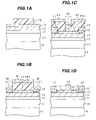
- FIGS. 1A to 1D are cross sectional views showing a semiconductor device and its manufacture method according to a first embodiment of the invention.
- FIGS. 2A , 2 B and 2 C are cross sectional views showing modifications of the embodiment shown in FIGS. 1A to 1D .
- FIG. 3 is a table showing the comparison of characteristics between samples according to the first embodiment and related art.
- FIGS. 4A and 4B are cross sectional views of a semiconductor device according to a second embodiment of the invention and a modification thereof.
- FIG. 5 is a table showing the comparison of characteristics between samples according to the second embodiment shown in FIGS. 4A and 4B and related art.
- FIGS. 6A and 6B are cross sectional views showing the structures of a semiconductor device according to a further embodiment of the invention and a modification thereof.
- FIGS. 7A and 7B are cross sectional views showing the structure of a semiconductor device according to a still further embodiment of the invention and a modification thereof.
- FIGS. 8A to 8D are cross sectional views and graphs showing the structures of prior art and related semiconductor devices and their band structures.
- the n-type cap layer 8 is deposited not only under the gate electrode but also under the source electrode 6 and drain electrode 7 . Since the electron tunneling effects are suppressed, the contact resistances of the source electrode 6 and drain electrode 7 are increased by about two digits, to 10 ⁇ 3 to 10 ⁇ 4 ⁇ cm 2 , as compared to a conventional device. The source series resistance is also increased so that the mutual conductance lowers.
- a two-terminal reverse leak current between the gate and drain measured was 100 ⁇ A/mm.
- An object of the embodiment of this invention is to provide a compound semiconductor device and its manufacture method, capable of improving a gate breakdown voltage and suppressing an increase in contact resistances of source and drain electrodes and an increase in reverse leak current between the gate and drain.
- Another object of the embodiment of this invention is to provide a compound semiconductor device and its manufacture method, capable of realizing a high breakdown voltage of a gate electrode and suppressing an increase in contact resistances of source and drain electrodes, an increase in source series resistance, an increase in leak current between the gate and drain and an increase in leak current between the gate and source.
- Still another object of the embodiment of the invention is to provide a GaN type field effect transistor having improved characteristics.
- FIGS. 1A to 1D are cross sectional views showing a semiconductor device and its manufacture method according to the first embodiment.
- an undoped GaN channel (electron transfer) layer 10 is deposited to a thickness of about 3 ?m by metal organic vapor phase deposition (MOVPE).
- MOVPE metal organic vapor phase deposition
- a sapphire substrate may be used.
- the channel layer may be grown after a buffer layer is formed on the substrate.
- an undoped Al0.25Ga0.75N spacer layer 11 is deposited to a thickness of about 3 nm by MOVPE, next an n-type Al 0.25 Ga 0.75 N electron supply layer 12 doped with Si at a concentration of 1 ⁇ 10 17 cm ⁇ 3 or more is grown to a thickness of about 20 nm, and then an n-type GaN cap layer 13 doped with Si at a concentration of 1 ⁇ 10 17 cm ⁇ 3 or more, e.g., at 2 ⁇ 10 18 cm ⁇ 3 is deposited to a thickness of 10 nm or thinner, e.g., 5 nm, respectively by MOVPE. In this manner, a semiconductor lamination structure is formed by MOVPE.
- the surface of the n-type GaN cap layer 13 has a roughness of about 0.3 nm.
- the n-type GaN cap layer 13 having large piezo polarization and spontaneous polarization effects is formed on the n-type Al 0.25 Ga 0.75 N electron supply layer 12 , it is possible to raise the potential barrier of the semiconductor lamination structure and enlarge the size thereof in the thickness direction.
- the breakdown voltage relative to the gate electrode can be increased.
- this high gate breakdown voltage is inevitably followed by high source and drain resistances, with source and drain electrodes being formed on the n-type GaN cap layer 13 .
- Electron affinity of GaN is larger than that of AIGaN.
- the compound semiconductor having a larger electron affinity has a smaller band gap.
- a resist layer is coated on the surface of the semiconductor lamination structure, exposed and developed to form a photoresist pattern PR 1 .
- the photoresist pattern PR 1 has openings in the regions corresponding to the regions where the source and drain electrodes are to be formed.
- the cap layer 13 exposed in the openings are partially removed by dry etching using mixture gas of chlorine containing gas such as Cl 2 and inert gas. It is preferable to set the thickness of the left GaN cap layer to 2 nm or thinner.
- the photoresist pattern PR 1 is thereafter removed.
- the piezo polarization and spontaneous polarization effects of GaN are mitigated to lower the potential barrier and shorten the barrier length. If source/drain electrodes are formed on the thinned GaN layer, tunneling current becomes easy to flow so that the source/drain resistances can be lowered effectively.
- the roughness of the GaN surface of the recess portion formed through dry etching is controlled to be larger than the roughness of the GaN surface in the gate electrode forming region covered with the photoresist pattern PR 1 .
- the etching conditions are set so that the roughness of the GaN surface in the source/drain forming regions becomes at least 1.5 times as large as that in the gate electrode forming region.
- the roughness can be increased by raising a bias voltage and a pressure (a bias voltage is raised to 100 V or higher although it is usually 50 V or lower, and a pressure is raised to about 4 Pa although it is usually about 2 Pa).
- a bias voltage is raised to 100 V or higher although it is usually 50 V or lower, and a pressure is raised to about 4 Pa although it is usually about 2 Pa.
- the roughness of the GaN surface in the source/drain electrode forming regions is set to a range of 1.5 times to 10 times as large as that of the GaN surface in the gate electrode forming region. With such a surface roughness, the contact area of an electrode formed on the rough surface is increased so that the contact resistance can be lowered.
- N atoms near in the surface layer are allowed to escape to the extension so that N vacancies are formed.
- These N vacancies function as an n-type donor so that a high concentration n-type layer is formed on the GaN surface.
- a new photoresist pattern PR 2 is formed covering the terrace (non-etched) portion of the GaN cap layer and the stepping-down edge portions extending to the adjacent recess (etched) portions.
- a metal layer M 1 is then deposited, the metal layer M 1 being a lamination of a Ti layer and an Al layer.
- the metal layer M 1 is deposited on the resist pattern PR 2 is lift off together with the resist pattern PR 2 .
- a source electrode 15 and a drain electrode 16 are left on the surfaces of the recess portions of the semiconductor lamination structure.
- the source electrode 15 and drain electrode 16 are formed spaced apart from the terrace portion of the dap layer 13 .
- the cap layer 13 on which a gate electrode is to be formed has steps in front of the source electrode 15 and drain electrode 16 .
- the source/drain electrodes are not in contact with the upper surface of the GaN layer. It is not necessary to dispose the source/drain electrodes too far away from the steps of the terrace portions. This layout is important in terms of leak current reduction to be later described.
- the source electrode 15 and drain electrode 16 are subjected to annealing at 450° C. to 900° C.
- Reaction allowed during annealing is likely to be enhanced because of the enlarged contact area between the cap layer 13 and electrodes 15 , 16 formed by the large roughness.
- a new photoresist pattern PR 3 is formed having a gate electrode opening within the gate electrode forming region.
- the gate electrode opening is formed narrower than the terrace width of the cap layer 13 .
- the gate length of the gate electrode is set to about 1 ⁇ m.
- a metal layer M 2 is deposited by stacking an Ni layer and an Au layer.
- the metal layer M 2 deposited on the photoresist pattern PR 3 is lifted off together with the photoresist pattern PR 3 .
- the gate electrode 14 is formed on the cap layer 13 .
- an SiN layer 17 is deposited by CVD to a thickness of, for example, 20 nm, and the unnecessary SiN layer on the surfaces of the electrodes is removed to expose the electrodes to thus complete a semiconductor device.
- the peak of the potential energy in the semiconductor lamination structure can be made high, the barrier can be broadened (the potential barrier peak is shifted away from the surface), the tunneling current can be reduced and the gate breakdown voltage can be raised.
- the n-type GaN cap layer 13 is thinned under the source electrode 15 and drain electrode 16 , the peak of the potential energy is lowered and the barrier length is shortened. The contact resistance of the source electrode 15 and drain electrode 16 can therefore be lowered. Since the source resistance associated with the source electrode 15 is lowered, the mutual conductance can be improved.
- the passivation film 17 formed on the surface of the n-type GaN cap layer 13 can expel holes induced near at the interface between the cap layer 13 and the passivation film 17 back into the inside. It is therefore possible to lower the potential peak energy of the conduction band at the interface between the n-type AlGaN electron supply layer and n-type GaN cap layer to be lower than that otherwise raised by a piezo electric field in the cap layer. An increase in leak current can be suppressed because there are gaps between the recessed bottom surfaces of the n-type GaN cap layer 13 with the source electrode 15 and drain electrode 16 formed thereon and the terrace portion surface of the n-type GaN cap layer 13 with the gate electrode 14 formed thereon.
- a sufficiently high gate breakdown voltage can be obtained by the structure shown in FIG. 1D .
- the leak current between the gate and drain cannot be said at a sufficiently low level.
- FIGS. 2A to 2C show a modification of the first embodiment shown in FIGS. 1A to 1D .
- a notch 18 was formed in a passivation layer 17 between the gate electrode 14 and drain electrode 16 to cut the passivation layer 17 at a position between the two electrodes.
- the involvement of the notch 18 reduced the leak current.
- This phenomenon may be ascribed to that leak current increases if the interface between the n-type GaN cap layer 13 and passivation layer 17 forms a continuous plane and the leak current reduces if the interface is cut at any position or is stepped down or above.
- FIG. 2B shows another structure for reducing the leak current.
- a notch 19 was formed at least in the cap layer 13 in the areas between the gate electrode 14 and the source electrode 15 and between the gate electrode and the drain electrode 16 , extending from the surface of the n-type GaN cap layer 13 , traversing the GaN cap layer in a depth direction and reaching the inside of the AlGaN electron supply layer 12 , and thereafter a passivation layer 17 was formed.
- Leak current can be expected to be reduced by the interface between the passivation layer 17 and n-type GaN cap layer 13 which interface has steps between the adjacent electrodes and changes its direction abruptly.
- the roughness of the surfaces of the GaN layer under the source and drain electrodes is not limited only to those being formed by etching.
- FIG. 2C illustrates a process of exposing the recessed surfaces of a GaN cap layer in the source/drain forming regions to plasma P, to make the surfaces rough and increase the roughness. Exposure to the plasma P increases the surface roughness R.
- FIG. 3 is a table showing the measured characteristics of samples having the structures shown in FIGS. 1D and 2B .
- the characteristics of samples having the related art structure shown in FIG. 8C were also measured for the purpose of comparison.
- a contact resistance was 1 ⁇ 10 ⁇ 3 to 1 ⁇ 10 ⁇ 4 ⁇ cm ⁇ 2 for the structure according to the related art.
- the contact resistances of the structures shown in FIGS. 1D and 2B were 7 ⁇ 10 ⁇ 6 to 3 ⁇ 10 ⁇ 5 ⁇ cm ⁇ 2 , improved by more than one digit, approximately by two digits.
- An on-resistance was about 12 ⁇ mm for the structure shown in FIG. 8C according to the related art. In contract, the on-resistance was approximately halved to 6 to 8 ⁇ mm for the structures shown in FIGS. 1D and 2B .
- a two-terminal reverse current between gate and drain was 100 ⁇ A/mm at 100 V for the structure shown in FIG. 8C according to related art.
- the two-terminal reverse current was halved to 50 ⁇ A/mm for the structure shown in FIG. 1D , and for the structure shown in FIG. 2B , reduced to 1 ⁇ A/mm, about 1/100 times as that of the related art structure.
- a mutual conductance gm was 140 mS/mm for the structure shown in FIG. 8C according to related art. In contrast, the mutual conductance was increased considerably to 220 mS/mm for the structures shown in FIGS. 1D and 2B .
- the characteristics can be improved greatly by the first embodiment and its modification, as compared to the related art characteristics.
- the n-type GaN cap layer under the source and drain electrodes is partially removed.
- the n-type GaN layer may be removed completely.
- FIGS. 4A and 4B are cross sectional views showing a semiconductor device and its manufacture method according to another embodiment of the invention and a modification thereof.
- the n-type GaN cap layer 13 is etched by almost the whole thickness thereof. In this case, roughness on the etched surface leaves a partial n-type GaN cap layer 13 in the less-etched area, and in the remaining surface area, partially etches the AlGaN electron supply layer 12 .
- a source electrode 15 and a drain electrode 16 are deposited, these electrodes contact the n-type GaN cap layer 13 in a partial area and the n-type AlGaN layer 12 in the other area.
- the resistance increasing effects of the n-type GaN layer 13 can be minimized and the exposed area of the AlGaN layer 12 containing Al can be made small so that the surface oxidation can be prevented effectively.
- the electrode contact area is increased by the surface roughness, the contact resistance can be lowered.
- the surface roughness provides the surface n-type impurity concentration increasing effects and the annealing reaction enhancing effects.
- FIG. 4B shows the structure shown in FIG. 4A modified in such a manner that notches 19 are formed extending from the surface of the n-type GaN cap layer 13 , traversing the cap layer 13 , to the inside of the AlGaN electron supply layer 12 .
- FIG. 5 is a table showing the measured characteristics of samples having the structures shown in FIGS. 4A and 4B .
- the characteristics of samples having the related art structure shown in FIG. 8C were also measured for the purpose of comparison.
- a contact resistance was 5 ⁇ 10 ⁇ 6 to 1 ⁇ 10 ⁇ 5 ⁇ cm ⁇ 2 for both the structures shown in FIGS. 4A and 4B , being improved considerably as compared to related art, being improved more than that of the structures shown in FIGS. 1D and 2B .
- An on-resistance was approximately halved to 6 to 7 ?mm as compared to the related art, being stabilized further than that of the structures shown in FIGS. 1D and 2B .
- a two-terminal reverse current between gate and drain was 50 ⁇ A/mm for the structure shown in FIG. 4A similar to that of the structure shown in FIG. 1D .
- the two-terminal reverse current was 1 ⁇ A/mm for the structure shown in FIG. 4B similar to that of the structure shown in FIG. 2B .
- a mutual conductance gm was 250 mS/mm for both the structures shown in FIGS. 4A and 4B , being considerably improved as compared to related art and also to the structures shown in FIGS. 1D and 2B .
- each recess portion under the source or drain electrode is not limited only to the intermediate position in the n-type GaN cap layer 13 or to the interface between the n-type GaN cap layer 13 and underlying n-type AlGaN layer 12 .
- FIG. 6A shows the structure that the recess portions partially enter the inside of the n-type AlGaN layer 12 .
- the etching continues until the n-type AlGaN layer 12 is partially etched. This etching amount is set to, for example, 10 nm or thinner in the depth direction.
- the other processes are similar to those described with reference to FIGS. 1A to 1D .
- FIG. 6B shows the structure shown in FIG. 6A modified in such a manner that notches 19 are formed extending from the surface of the n-type GaN cap layer 13 to the inside of the AlGaN electron supply layer 12 .
- leak current can be expected to be reduced more than that of the structure shown in FIG. 6A .
- FIG. 7A shows the structure that the depth of the recess portion under the source electrode is made different from that under the drain electrode.
- the recess portion under the drain electrode 16 reaches an intermediate depth of the n-type GaN cap layer 13
- the recess portion under the source electrode 15 reaches the interface between the n-type GaN cap layer 13 and n-type AlGaN electron supply layer 12 similar to the structure shown in FIG. 4A .
- the contact resistance of the source electrode 15 as well as the source resistance can be expected to be lowered more.
- FIG. 7B shows the structure that the recess portion under the source electrode 15 is made deeper.
- the recess portion under the source electrode 15 is made deeper by partially removing the n-type AlGaN electron supply layer 12 . It can be expected that both the source contact resistance and the source resistance can be lowered more.
- Etching using different resist masks can be performed to form recess portions under the source electrode 15 and drain electrode 16 having different depths as shown in FIGS. 7A and 7B .
- the present invention has been described in connection with the preferred embodiments.
- the invention is not limited only to the above embodiments.
- GaN and AlGaN are used in the embodiments, similar advantageous effects can be expected even by using InxGa 1-x N (0 ⁇ x ⁇ 1) and In p Al q Ga 1-p-q N(0 ⁇ p ⁇ 1), 0 ⁇ q ⁇ 1, 0 ⁇ p+q ⁇ 1) which contain In and having a critical film thickness or thinner. It will be apparent to those skilled in the art that other various modifications, improvements, combinations, and the like can be made.
Abstract
A compound semiconductor device has: a substrate; a GaN channel layer; an n-type AlqGal-qN (0<q (1) electron supply layer; an n-type GaN cap layer; a gate electrode disposed on the cap layer and forming a Schottky contact; recesses formed on both sides of the gate electrode on source and drain sides by at least partially removing the cap layer, the recesses having a bottom surface of a roughness larger than a roughness of a surface of the cap layer under the gate electrode; a source electrode disposed on the bottom surface of the recess on the source side; and a drain electrode disposed on the bottom surface of the recess on the drain side.
Description
This application is a divisional application of U.S. Ser. No. 10/764,486, filed Jan. 27, 2004 now U.S. Pat. No. 7,132,699, and is based on and claims priority of Japanese Patent Application No. 2003-17308 filed on Jan. 27, 2003, the entire contents of which are incorporated herein by reference.
A) Field of the Invention
The present invention relates to a semiconductor device and its manufacture method, and more particularly to a compound semiconductor device having a channel (electron transfer) layer made of GaN group compound semiconductor and its manufacture method.
B) Description of the Related Art
GaN field effect transistors have been developed which use as a channel layer a GaN layer in contact with an AlGaN/GaN hetero junction. GaN has a wide band gap, a high breakdown electric field strength (intensity) and a high saturated electron velocity and is quite promising as the material of devices of high voltage operation and high output power.
A power device in a cellular phone base station is required to operate at a high voltage of 40 V or higher so that GaN field effect transistors present bright prospects. High voltage operation requires a high gate breakdown voltage (a high reverse gate voltage at a predetermined gate leak current, and a high gate-drain voltage at a predetermined gate-drain leak current).
Referring to FIG. 8A , on a substrate made of sapphire or SiC, a buffer layer of GaN or AlN is formed when necessary, to form a work substrate 1. On this work substrate 1, a GaN channel (electron transfer) layer 2 is formed. An AlGaN electron supply layer 3 is formed on the GaN channel layer 2. The electron supply layer 3 has an n-type conductivity doped with, for example, Si and can supply electrons to the channel layer 2.
On the electron supply layer 3, a gate electrode 5, a source electrode 6 and a drain electrode 7 are formed, and the surface of the electron supply layer 3 is covered with a passivation film 4.
A tunneling current I through a potential barrier of length L has the following relation.
|∝exp(−C×L)
|∝exp(−C×L)
The tunneling current increases as the potential barrier length L becomes short. As shown in FIG. 8B , there is a region where the potential energy of the conduction band in the AlGaN layer increases steeply and the potential barrier length becomes shorter. Through this region, electrons supplied from the surface (gate electrode) are likely to be tunneled. A two-terminal breakdown voltage is about several ten V which is insufficient for high voltage operation.
As shown in FIG. 8C , as compared to the structure shown in FIG. 8A , an n-type GaN cap layer 8 is disposed between the electron supply layer 3 and gate electrode 5.
The band structure is changed in this manner so that a tunneling current from the substrate surface can be suppressed. It is possible to set a two-terminal gate breakdown voltage to 150 V or higher and a three-terminal gate breakdown voltage to 50 V or higher (for example, refer to Japanese Patent Laid-open Publication No. 2002-359256 which is incorporated herein by reference).
Japanese Patent Laid-open Publication No. 2001-230407 proposes a field effect transistor whose GaN cap layer under the source and drain electrodes is removed.
Japanese Patent Laid-open Publication No. 2002-16087 proposes a field effect transistor whose source and drain electrodes are formed on an AlGaN electron supply layer and a gate electrode is formed on an InGaN Schottky-contact-forming layer.
According to one aspect of the present invention, there is provided a compound semiconductor device comprising: a substrate; a channel layer disposed above the substrate and consisting essentially of GaN; an electron supply layer disposed above the channel layer and consisting essentially of n-type AlqGa1-qN (0<q≦1); a cap layer disposed above the electron supply layer and consisting essentially of n-type GaN; a gate electrode disposed on the cap layer and forming a Schottky contact; recesses formed on both sides of the gate electrode on source and drain sides by removing at least part of the cap layer, the recess having a bottom surface of a roughness larger than a roughness of a surface of the cap layer under the gate electrode; a source electrode disposed on the bottom surface of recess on the source side; and a drain electrode disposed on the bottom surface of the recess on the drain side.
According to another aspect of the present invention, there is provided a method of manufacturing a compound semiconductor device comprising the steps of: (a) epitaxially laminating, above a substrate, a channel layer consisting essentially of GaN, an electron supply layer consisting essentially of n-type AqGa1-qN(0<q≦1) and a cap layer consisting essentially of n-type GaN, in this order recited; (b) forming a gate electrode on the cap layer, the gate electrode having a Schottky contact; (c) etching at least part of the cap layer to form recesses on both sides of the gate electrode on source and drain sides, in such a manner that a bottom surfaces of the recesses have a roughness larger than a roughness of a surface of the cap layer under the gate electrode; and (d) forming a source electrode and a drain electrode on the bottom surfaces of the recesses on the source and drain sides.
The source and drain resistances can be lowered by forming the recesses under the source and drain electrodes by removing at least part of the cap layer. The contact resistance can be lowered by providing the bottom surface of the recess with roughness.
By forming a notch in the cap layer between the gate electrode and drain electrode, leak current between the gate and drain can be reduced.
As above, it is possible to improve the breakdown voltage relative to the gate electrode and suppress an increase in contact resistance of source and drain electrodes.
In the GaN-FET structure shown in FIG. 8C , the n-type cap layer 8 is deposited not only under the gate electrode but also under the source electrode 6 and drain electrode 7. Since the electron tunneling effects are suppressed, the contact resistances of the source electrode 6 and drain electrode 7 are increased by about two digits, to 10−3 to 10−4 Ωcm2, as compared to a conventional device. The source series resistance is also increased so that the mutual conductance lowers.
A two-terminal reverse leak current between the gate and drain measured was 100 μA/mm.
It is desired to have a high breakdown voltage relative to the gate electrode and lower the contact resistances of the source and drain electrodes. It is also desired to reduce a two-terminal reverse leak current between the gate and drain.
An object of the embodiment of this invention is to provide a compound semiconductor device and its manufacture method, capable of improving a gate breakdown voltage and suppressing an increase in contact resistances of source and drain electrodes and an increase in reverse leak current between the gate and drain.
Another object of the embodiment of this invention is to provide a compound semiconductor device and its manufacture method, capable of realizing a high breakdown voltage of a gate electrode and suppressing an increase in contact resistances of source and drain electrodes, an increase in source series resistance, an increase in leak current between the gate and drain and an increase in leak current between the gate and source.
Still another object of the embodiment of the invention is to provide a GaN type field effect transistor having improved characteristics.
Embodiments of the invention will be described with reference to the accompanying drawings.
On the channel layer 10, an undoped Al0.25Ga0.75N spacer layer 11 is deposited to a thickness of about 3 nm by MOVPE, next an n-type Al0.25Ga0.75N electron supply layer 12 doped with Si at a concentration of 1×1017 cm−3 or more is grown to a thickness of about 20 nm, and then an n-type GaN cap layer 13 doped with Si at a concentration of 1×1017cm−3 or more, e.g., at 2×1018 cm−3 is deposited to a thickness of 10 nm or thinner, e.g., 5 nm, respectively by MOVPE. In this manner, a semiconductor lamination structure is formed by MOVPE. The surface of the n-type GaN cap layer 13 has a roughness of about 0.3 nm.
Since the n-type GaN cap layer 13 having large piezo polarization and spontaneous polarization effects is formed on the n-type Al0.25Ga0.75N electron supply layer 12, it is possible to raise the potential barrier of the semiconductor lamination structure and enlarge the size thereof in the thickness direction. The breakdown voltage relative to the gate electrode can be increased. However, this high gate breakdown voltage is inevitably followed by high source and drain resistances, with source and drain electrodes being formed on the n-type GaN cap layer 13.
Electron affinity of GaN is larger than that of AIGaN. In the case of GaN and AlGaN, the compound semiconductor having a larger electron affinity has a smaller band gap. When surfaces having different electron affinities are made in contact, electrons are likely to be accumulated in the substance having a larger electron affinity.
A resist layer is coated on the surface of the semiconductor lamination structure, exposed and developed to form a photoresist pattern PR1. The photoresist pattern PR1 has openings in the regions corresponding to the regions where the source and drain electrodes are to be formed. The cap layer 13 exposed in the openings are partially removed by dry etching using mixture gas of chlorine containing gas such as Cl2 and inert gas. It is preferable to set the thickness of the left GaN cap layer to 2 nm or thinner. The photoresist pattern PR1 is thereafter removed.
As the GaN cap layer is thinned, the piezo polarization and spontaneous polarization effects of GaN are mitigated to lower the potential barrier and shorten the barrier length. If source/drain electrodes are formed on the thinned GaN layer, tunneling current becomes easy to flow so that the source/drain resistances can be lowered effectively.
If the interface between AlGaN/GaN is steep, the piezo effects and the like are likely to occur, whereas if the interface is gentle, the piezo effects are greatly suppressed. In the latter case, a rise in the band is eliminated and ohmic contact becomes easy to be established.
The roughness of the GaN surface of the recess portion formed through dry etching is controlled to be larger than the roughness of the GaN surface in the gate electrode forming region covered with the photoresist pattern PR1. The etching conditions are set so that the roughness of the GaN surface in the source/drain forming regions becomes at least 1.5 times as large as that in the gate electrode forming region.
More specifically, the roughness can be increased by raising a bias voltage and a pressure (a bias voltage is raised to 100 V or higher although it is usually 50 V or lower, and a pressure is raised to about 4 Pa although it is usually about 2 Pa). By adopting such etching conditions not used by general selective etching, the roughness can be increased.
For example, the roughness of the GaN surface in the source/drain electrode forming regions is set to a range of 1.5 times to 10 times as large as that of the GaN surface in the gate electrode forming region. With such a surface roughness, the contact area of an electrode formed on the rough surface is increased so that the contact resistance can be lowered.
If the roughness becomes large, nitrogen (N) atoms near in the surface layer are allowed to escape to the extension so that N vacancies are formed. These N vacancies function as an n-type donor so that a high concentration n-type layer is formed on the GaN surface.
As shown in FIG. 1B , a new photoresist pattern PR2 is formed covering the terrace (non-etched) portion of the GaN cap layer and the stepping-down edge portions extending to the adjacent recess (etched) portions. A metal layer M1 is then deposited, the metal layer M1 being a lamination of a Ti layer and an Al layer. The metal layer M1 is deposited on the resist pattern PR2 is lift off together with the resist pattern PR2. A source electrode 15 and a drain electrode 16 are left on the surfaces of the recess portions of the semiconductor lamination structure.
The source electrode 15 and drain electrode 16 are formed spaced apart from the terrace portion of the dap layer 13. In other words, the cap layer 13 on which a gate electrode is to be formed has steps in front of the source electrode 15 and drain electrode 16. The source/drain electrodes are not in contact with the upper surface of the GaN layer. It is not necessary to dispose the source/drain electrodes too far away from the steps of the terrace portions. This layout is important in terms of leak current reduction to be later described.
The source electrode 15 and drain electrode 16 are subjected to annealing at 450° C. to 900° C.
Reaction allowed during annealing is likely to be enhanced because of the enlarged contact area between the cap layer 13 and electrodes 15, 16 formed by the large roughness.
In the above manner, ohmic contact of the source/drain electrodes is formed on the semiconductor lamination structure.
As shown in FIG. 1C , a new photoresist pattern PR3 is formed having a gate electrode opening within the gate electrode forming region. The gate electrode opening is formed narrower than the terrace width of the cap layer 13. For example, the gate length of the gate electrode is set to about 1 μm.
A metal layer M2 is deposited by stacking an Ni layer and an Au layer. The metal layer M2 deposited on the photoresist pattern PR3 is lifted off together with the photoresist pattern PR3. In this manner, the gate electrode 14 is formed on the cap layer 13.
As shown in FIG. 1D , an SiN layer 17 is deposited by CVD to a thickness of, for example, 20 nm, and the unnecessary SiN layer on the surfaces of the electrodes is removed to expose the electrodes to thus complete a semiconductor device.
In the structure shown in FIG. 1D , since the n-type GaN cap layer 13 is disposed between the gate electrode 14 and electron supply layer 12, the peak of the potential energy in the semiconductor lamination structure can be made high, the barrier can be broadened (the potential barrier peak is shifted away from the surface), the tunneling current can be reduced and the gate breakdown voltage can be raised.
Since the n-type GaN cap layer 13 is thinned under the source electrode 15 and drain electrode 16, the peak of the potential energy is lowered and the barrier length is shortened. The contact resistance of the source electrode 15 and drain electrode 16 can therefore be lowered. Since the source resistance associated with the source electrode 15 is lowered, the mutual conductance can be improved.
The passivation film 17 formed on the surface of the n-type GaN cap layer 13 can expel holes induced near at the interface between the cap layer 13 and the passivation film 17 back into the inside. It is therefore possible to lower the potential peak energy of the conduction band at the interface between the n-type AlGaN electron supply layer and n-type GaN cap layer to be lower than that otherwise raised by a piezo electric field in the cap layer. An increase in leak current can be suppressed because there are gaps between the recessed bottom surfaces of the n-type GaN cap layer 13 with the source electrode 15 and drain electrode 16 formed thereon and the terrace portion surface of the n-type GaN cap layer 13 with the gate electrode 14 formed thereon.
A sufficiently high gate breakdown voltage can be obtained by the structure shown in FIG. 1D . However, the leak current between the gate and drain cannot be said at a sufficiently low level.
As shown in FIG. 2A , a notch 18 was formed in a passivation layer 17 between the gate electrode 14 and drain electrode 16 to cut the passivation layer 17 at a position between the two electrodes. The involvement of the notch 18 reduced the leak current.
This phenomenon may be ascribed to that leak current increases if the interface between the n-type GaN cap layer 13 and passivation layer 17 forms a continuous plane and the leak current reduces if the interface is cut at any position or is stepped down or above.
The roughness of the surfaces of the GaN layer under the source and drain electrodes is not limited only to those being formed by etching.
A contact resistance was 1×10⁻³ to 1×10⁻⁴ Ωcm−2 for the structure according to the related art. In contrast, the contact resistances of the structures shown in FIGS. 1D and 2B were 7×10⁻⁶ to 3×10⁻⁵ Ωcm−2, improved by more than one digit, approximately by two digits.
An on-resistance was about 12 Ωmm for the structure shown in FIG. 8C according to the related art. In contract, the on-resistance was approximately halved to 6 to 8 Ωmm for the structures shown in FIGS. 1D and 2B .
A two-terminal reverse current between gate and drain was 100 μA/mm at 100 V for the structure shown in FIG. 8C according to related art. In contrast, the two-terminal reverse current was halved to 50 μA/mm for the structure shown in FIG. 1D , and for the structure shown in FIG. 2B , reduced to 1 μA/mm, about 1/100 times as that of the related art structure.
A mutual conductance gm was 140 mS/mm for the structure shown in FIG. 8C according to related art. In contrast, the mutual conductance was increased considerably to 220 mS/mm for the structures shown in FIGS. 1D and 2B . The characteristics can be improved greatly by the first embodiment and its modification, as compared to the related art characteristics.
In the embodiment shown in FIGS. 1A to 1D , the n-type GaN cap layer under the source and drain electrodes is partially removed. The n-type GaN layer may be removed completely.
As shown in FIG. 4A , in the etching process shown in FIG. 1A , the n-type GaN cap layer 13 is etched by almost the whole thickness thereof. In this case, roughness on the etched surface leaves a partial n-type GaN cap layer 13 in the less-etched area, and in the remaining surface area, partially etches the AlGaN electron supply layer 12.
As a source electrode 15 and a drain electrode 16 are deposited, these electrodes contact the n-type GaN cap layer 13 in a partial area and the n-type AlGaN layer 12 in the other area. The resistance increasing effects of the n-type GaN layer 13 can be minimized and the exposed area of the AlGaN layer 12 containing Al can be made small so that the surface oxidation can be prevented effectively. In addition, since the electrode contact area is increased by the surface roughness, the contact resistance can be lowered. The surface roughness provides the surface n-type impurity concentration increasing effects and the annealing reaction enhancing effects.
A contact resistance was 5×10⁻⁶ to 1×10⁻⁵ Ωcm−2 for both the structures shown in FIGS. 4A and 4B , being improved considerably as compared to related art, being improved more than that of the structures shown in FIGS. 1D and 2B . An on-resistance was approximately halved to 6 to 7 ?mm as compared to the related art, being stabilized further than that of the structures shown in FIGS. 1D and 2B .
A two-terminal reverse current between gate and drain was 50 μA/mm for the structure shown in FIG. 4A similar to that of the structure shown in FIG. 1D . The two-terminal reverse current was 1 μA/mm for the structure shown in FIG. 4B similar to that of the structure shown in FIG. 2B .
A mutual conductance gm was 250 mS/mm for both the structures shown in FIGS. 4A and 4B , being considerably improved as compared to related art and also to the structures shown in FIGS. 1D and 2B .
The depth of each recess portion under the source or drain electrode is not limited only to the intermediate position in the n-type GaN cap layer 13 or to the interface between the n-type GaN cap layer 13 and underlying n-type AlGaN layer 12.
Etching using different resist masks can be performed to form recess portions under the source electrode 15 and drain electrode 16 having different depths as shown in FIGS. 7A and 7B .
The present invention has been described in connection with the preferred embodiments. The invention is not limited only to the above embodiments. For example, although GaN and AlGaN are used in the embodiments, similar advantageous effects can be expected even by using InxGa1-xN (0≦x<1) and InpAlqGa1-p-qN(0≦p<1), 0≦q<1, 0<p+q≦1) which contain In and having a critical film thickness or thinner. It will be apparent to those skilled in the art that other various modifications, improvements, combinations, and the like can be made.
Claims (5)
1. A method of manufacturing a compound semiconductor device comprising the steps of:
(a) epitaxially laminating above a substrate a channel layer consisting essentially of GaN, an electron supply layer consisting essentially of n-type AlqGal-qN (0<q (1) and a cap layer consisting essentially of n-type GaN, in this order recited;
(b) forming a gate electrode on said cap layer, said gate electrode having a Schottky contact;
(c) etching at least part of the cap layer to form recesses on both sides of said gate electrode on source and drain sides, in such a manner that a bottom surfaces of said recesses have a roughness larger than a roughness of a surface of said cap layer under said gate electrode; and
(d) forming a source electrode and a drain electrode on the bottom surfaces of said recesses on the source and drain sides.
2. The method of manufacturing a compound semiconductor device according to claim 1 , wherein said step (c) partially leaves said cap layer and partially exposes said electron supply layer by positively utilizing said roughness, and said step (d) forms one or both of said source and drain electrodes so as to make one or both contact both said cap layer and said electron supply layer.
3. The method of manufacturing a compound semiconductor device according to claim 1 , further comprising a step of exposing the surfaces of said recesses to plasma after said step (c).
4. The method of manufacturing a compound semiconductor device according to claim 1 , wherein said step (c) includes etching said recess on the source side by using a mask and etching said recess on the drain side by using another mask.
5. The method of manufacturing a compound semiconductor device according to claim 1 , further comprising a step of forming a notch through said cap layer, said notch traversing in a depth direction said cap layer at least between said gate electrode and said drain electrode or between said source electrode and said gate electrode.
Priority Applications (1)
| Application Number | Priority Date | Filing Date | Title |
|---|---|---|---|
| US11/541,571 US7407859B2 (en) | 2003-01-27 | 2006-10-03 | Compound semiconductor device and its manufacture |
Applications Claiming Priority (4)
| Application Number | Priority Date | Filing Date | Title |
|---|---|---|---|
| JP2003-017308 | 2003-01-27 | ||
| JP2003017308A JP4077731B2 (en) | 2003-01-27 | 2003-01-27 | Compound semiconductor device and manufacturing method thereof |
| US10/764,486 US7132699B2 (en) | 2003-01-27 | 2004-01-27 | Compound semiconductor device and its manufacture |
| US11/541,571 US7407859B2 (en) | 2003-01-27 | 2006-10-03 | Compound semiconductor device and its manufacture |
Related Parent Applications (1)
| Application Number | Title | Priority Date | Filing Date |
|---|---|---|---|
| US10/764,486 Division US7132699B2 (en) | 2003-01-27 | 2004-01-27 | Compound semiconductor device and its manufacture |
Publications (2)
| Publication Number | Publication Date |
|---|---|
| US20070026552A1 US20070026552A1 (en) | 2007-02-01 |
| US7407859B2 true US7407859B2 (en) | 2008-08-05 |
Family
ID=32904491
Family Applications (2)
| Application Number | Title | Priority Date | Filing Date |
|---|---|---|---|
| US10/764,486 Expired - Lifetime US7132699B2 (en) | 2003-01-27 | 2004-01-27 | Compound semiconductor device and its manufacture |
| US11/541,571 Active 2024-05-22 US7407859B2 (en) | 2003-01-27 | 2006-10-03 | Compound semiconductor device and its manufacture |
Family Applications Before (1)
| Application Number | Title | Priority Date | Filing Date |
|---|---|---|---|
| US10/764,486 Expired - Lifetime US7132699B2 (en) | 2003-01-27 | 2004-01-27 | Compound semiconductor device and its manufacture |
Country Status (2)
| Country | Link |
|---|---|
| US (2) | US7132699B2 (en) |
| JP (1) | JP4077731B2 (en) |
Cited By (3)
| Publication number | Priority date | Publication date | Assignee | Title |
|---|---|---|---|---|
| US20060197107A1 (en) * | 2005-03-03 | 2006-09-07 | Fujitsu Limited | Semiconductor device and production method thereof |
| US20070254419A1 (en) * | 2003-10-23 | 2007-11-01 | Matsushida Electric Industrial Co., Ltd. | Semiconductor device and method for fabricating the same |
| US8766276B2 (en) | 2011-11-22 | 2014-07-01 | Renesas Electronics Corporation | Semiconductor device and method of manufacturing semiconductor device |
Families Citing this family (49)
| Publication number | Priority date | Publication date | Assignee | Title |
|---|---|---|---|---|
| US7501669B2 (en) | 2003-09-09 | 2009-03-10 | Cree, Inc. | Wide bandgap transistor devices with field plates |
| US9773877B2 (en) | 2004-05-13 | 2017-09-26 | Cree, Inc. | Wide bandgap field effect transistors with source connected field plates |
| US7554123B2 (en) * | 2004-08-25 | 2009-06-30 | Sensor Electronic Technology, Inc. | Ohmic contact for nitride-based semiconductor device |
| US20100140627A1 (en) * | 2005-01-10 | 2010-06-10 | Shelton Bryan S | Package for Semiconductor Devices |
| JP4866007B2 (en) * | 2005-01-14 | 2012-02-01 | 富士通株式会社 | Compound semiconductor device |
| US11791385B2 (en) * | 2005-03-11 | 2023-10-17 | Wolfspeed, Inc. | Wide bandgap transistors with gate-source field plates |
| JP4912604B2 (en) * | 2005-03-30 | 2012-04-11 | 住友電工デバイス・イノベーション株式会社 | Nitride semiconductor HEMT and manufacturing method thereof. |
| JP4536568B2 (en) * | 2005-03-31 | 2010-09-01 | 住友電工デバイス・イノベーション株式会社 | Method for manufacturing FET |
| JP2007194588A (en) * | 2005-12-20 | 2007-08-02 | Sony Corp | Field-effect transistor, semiconductor device having the same, and semiconductor device manufacturing method |
| JP2007220895A (en) * | 2006-02-16 | 2007-08-30 | Matsushita Electric Ind Co Ltd | Nitride semiconductor device and its manufacturing method |
| JP5231719B2 (en) * | 2006-03-30 | 2013-07-10 | 富士通株式会社 | Method for manufacturing field effect transistor |
| JP5207598B2 (en) | 2006-05-24 | 2013-06-12 | パナソニック株式会社 | Nitride semiconductor material, semiconductor element and method of manufacturing the same |
| JP5105160B2 (en) | 2006-11-13 | 2012-12-19 | クリー インコーポレイテッド | Transistor |
| JP2008211172A (en) * | 2007-01-31 | 2008-09-11 | Matsushita Electric Ind Co Ltd | Semiconductor device and method for fabricating the same |
| US8035130B2 (en) * | 2007-03-26 | 2011-10-11 | Mitsubishi Electric Corporation | Nitride semiconductor heterojunction field effect transistor having wide band gap barrier layer that includes high concentration impurity region |
| JP2009004504A (en) * | 2007-06-20 | 2009-01-08 | Fujitsu Ltd | Compound semiconductor device and method of manufacturing the same |
| US20100072484A1 (en) * | 2008-09-23 | 2010-03-25 | Triquint Semiconductor, Inc. | Heteroepitaxial gallium nitride-based device formed on an off-cut substrate |
| JP5566670B2 (en) * | 2008-12-16 | 2014-08-06 | 古河電気工業株式会社 | GaN-based field effect transistor |
| JP5564791B2 (en) | 2008-12-26 | 2014-08-06 | 富士通株式会社 | Compound semiconductor device and manufacturing method thereof |
| JP5595685B2 (en) * | 2009-07-28 | 2014-09-24 | パナソニック株式会社 | Semiconductor device |
| JP5638225B2 (en) * | 2009-11-11 | 2014-12-10 | 三菱電機株式会社 | Heterojunction field effect transistor and manufacturing method thereof |
| JP5625336B2 (en) * | 2009-11-30 | 2014-11-19 | サンケン電気株式会社 | Semiconductor device |
| JP5577681B2 (en) * | 2009-11-30 | 2014-08-27 | 住友電気工業株式会社 | Semiconductor device |
| DE102010016993A1 (en) * | 2010-05-18 | 2011-11-24 | United Monolithic Semiconductors Gmbh | Semiconductor device |
| CN103109369B (en) | 2010-06-24 | 2016-04-06 | 富士通株式会社 | Semiconductor device |
| JP5707763B2 (en) * | 2010-07-26 | 2015-04-30 | 住友電気工業株式会社 | Manufacturing method of semiconductor device |
| JP5845568B2 (en) | 2010-11-02 | 2016-01-20 | 富士通株式会社 | Semiconductor device and manufacturing method thereof |
| CN102064108B (en) * | 2010-11-12 | 2014-11-26 | 中国电子科技集团公司第五十五研究所 | Method for manufacturing medium/nitride composite structure enhanced field effect transistor |
| JP2012109366A (en) * | 2010-11-17 | 2012-06-07 | Sharp Corp | Nitride semiconductor device |
| KR101214742B1 (en) | 2010-12-09 | 2012-12-21 | 삼성전기주식회사 | Nitride based semiconductor device and method for manufacturing the same |
| JP5620347B2 (en) * | 2011-07-19 | 2014-11-05 | 富士通株式会社 | Compound semiconductor device |
| JP6035721B2 (en) * | 2011-09-27 | 2016-11-30 | 住友電気工業株式会社 | Manufacturing method of semiconductor device |
| US8884308B2 (en) * | 2011-11-29 | 2014-11-11 | Taiwan Semiconductor Manufacturing Company, Ltd. | High electron mobility transistor structure with improved breakdown voltage performance |
| JP5464218B2 (en) * | 2012-02-01 | 2014-04-09 | 富士通株式会社 | Method for manufacturing gallium nitride-based HEMT and gallium nitride-based HEMT |
| JP2014072377A (en) * | 2012-09-28 | 2014-04-21 | Fujitsu Ltd | Compound semiconductor device and manufacturing method of the same |
| JP6161246B2 (en) | 2012-09-28 | 2017-07-12 | トランスフォーム・ジャパン株式会社 | Semiconductor device and manufacturing method of semiconductor device |
| US9679981B2 (en) | 2013-06-09 | 2017-06-13 | Cree, Inc. | Cascode structures for GaN HEMTs |
| US9847411B2 (en) | 2013-06-09 | 2017-12-19 | Cree, Inc. | Recessed field plate transistor structures |
| US9755059B2 (en) * | 2013-06-09 | 2017-09-05 | Cree, Inc. | Cascode structures with GaN cap layers |
| JP5742912B2 (en) * | 2013-10-25 | 2015-07-01 | 富士通株式会社 | Compound semiconductor device and manufacturing method thereof |
| CN106340536A (en) * | 2016-08-05 | 2017-01-18 | 苏州捷芯威半导体有限公司 | Power semiconductor device and manufacturing method thereof |
| US9935051B2 (en) * | 2016-08-18 | 2018-04-03 | International Business Machines Corporation | Multi-level metallization interconnect structure |
| JP2018182247A (en) * | 2017-04-21 | 2018-11-15 | ルネサスエレクトロニクス株式会社 | Semiconductor device and method of manufacturing the same |
| WO2018208285A1 (en) * | 2017-05-09 | 2018-11-15 | Intel Corporation | Transistor arrangements with uneven gate-drain surfaces |
| JP6888224B2 (en) * | 2017-10-16 | 2021-06-16 | 住友電工デバイス・イノベーション株式会社 | Manufacturing method of semiconductor devices |
| JP7100241B2 (en) | 2017-12-20 | 2022-07-13 | 富士通株式会社 | Compound semiconductor device and its manufacturing method |
| US20200083360A1 (en) * | 2018-09-10 | 2020-03-12 | Intel Corporation | Iii-n transistors with polarization modulation |
| CN109742141A (en) * | 2018-12-03 | 2019-05-10 | 北京大学深圳研究生院 | A kind of GaN base HEMT device and preparation method thereof |
| CN110071173B (en) * | 2019-04-30 | 2023-04-18 | 英诺赛科(珠海)科技有限公司 | Semiconductor device and method for manufacturing the same |
Citations (11)
| Publication number | Priority date | Publication date | Assignee | Title |
|---|---|---|---|---|
| JPH1116852A (en) | 1997-06-25 | 1999-01-22 | Sumitomo Chem Co Ltd | Production of electrode for 3-5 compound semiconductor and 3-5 compound semiconductor device |
| JP2001102565A (en) | 1999-09-28 | 2001-04-13 | Toshiba Corp | Method of manufacturing semiconductor device |
| JP2001230407A (en) | 1999-12-08 | 2001-08-24 | Matsushita Electric Ind Co Ltd | Semiconductor device |
| US6316793B1 (en) | 1998-06-12 | 2001-11-13 | Cree, Inc. | Nitride based transistors on semi-insulating silicon carbide substrates |
| JP2002016087A (en) | 2000-06-29 | 2002-01-18 | Nec Corp | Semiconductor device |
| JP2002016312A (en) | 2000-06-27 | 2002-01-18 | Sanyo Electric Co Ltd | Nitride semiconductor element and its manufacturing method |
| US6399493B1 (en) | 2001-05-17 | 2002-06-04 | Advanced Micro Devices, Inc. | Method of silicide formation by silicon pretreatment |
| JP2002359256A (en) | 2001-05-31 | 2002-12-13 | Fujitsu Ltd | Field effect compound semiconductor device |
| US6528405B1 (en) | 2000-02-18 | 2003-03-04 | Motorola, Inc. | Enhancement mode RF device and fabrication method |
| US6639255B2 (en) | 1999-12-08 | 2003-10-28 | Matsushita Electric Industrial Co., Ltd. | GaN-based HFET having a surface-leakage reducing cap layer |
| US20040144991A1 (en) * | 2003-01-15 | 2004-07-29 | Fujitsu Limited | Compound semiconductor device and method for fabricating the same |
-
2003
- 2003-01-27 JP JP2003017308A patent/JP4077731B2/en not_active Expired - Lifetime
-
2004
- 2004-01-27 US US10/764,486 patent/US7132699B2/en not_active Expired - Lifetime
-
2006
- 2006-10-03 US US11/541,571 patent/US7407859B2/en active Active
Patent Citations (14)
| Publication number | Priority date | Publication date | Assignee | Title |
|---|---|---|---|---|
| JPH1116852A (en) | 1997-06-25 | 1999-01-22 | Sumitomo Chem Co Ltd | Production of electrode for 3-5 compound semiconductor and 3-5 compound semiconductor device |
| US6316793B1 (en) | 1998-06-12 | 2001-11-13 | Cree, Inc. | Nitride based transistors on semi-insulating silicon carbide substrates |
| JP2001102565A (en) | 1999-09-28 | 2001-04-13 | Toshiba Corp | Method of manufacturing semiconductor device |
| JP2001230407A (en) | 1999-12-08 | 2001-08-24 | Matsushita Electric Ind Co Ltd | Semiconductor device |
| US6639255B2 (en) | 1999-12-08 | 2003-10-28 | Matsushita Electric Industrial Co., Ltd. | GaN-based HFET having a surface-leakage reducing cap layer |
| US6528405B1 (en) | 2000-02-18 | 2003-03-04 | Motorola, Inc. | Enhancement mode RF device and fabrication method |
| JP2002016312A (en) | 2000-06-27 | 2002-01-18 | Sanyo Electric Co Ltd | Nitride semiconductor element and its manufacturing method |
| US6492669B2 (en) | 2000-06-29 | 2002-12-10 | Nec Corporation | Semiconductor device with schottky electrode having high schottky barrier |
| JP2002016087A (en) | 2000-06-29 | 2002-01-18 | Nec Corp | Semiconductor device |
| US6399493B1 (en) | 2001-05-17 | 2002-06-04 | Advanced Micro Devices, Inc. | Method of silicide formation by silicon pretreatment |
| JP2002359256A (en) | 2001-05-31 | 2002-12-13 | Fujitsu Ltd | Field effect compound semiconductor device |
| US20040144991A1 (en) * | 2003-01-15 | 2004-07-29 | Fujitsu Limited | Compound semiconductor device and method for fabricating the same |
| US7002189B2 (en) * | 2003-01-15 | 2006-02-21 | Fujitsu Limited | Compound semiconductor device |
| US20060054925A1 (en) * | 2003-01-15 | 2006-03-16 | Fujitsu Limited | Compound semiconductor device and method for fabricating the same |
Non-Patent Citations (1)
| Title |
|---|
| Japanese Office Action dated Nov. 6, 2007 with English translation. |
Cited By (3)
| Publication number | Priority date | Publication date | Assignee | Title |
|---|---|---|---|---|
| US20070254419A1 (en) * | 2003-10-23 | 2007-11-01 | Matsushida Electric Industrial Co., Ltd. | Semiconductor device and method for fabricating the same |
| US20060197107A1 (en) * | 2005-03-03 | 2006-09-07 | Fujitsu Limited | Semiconductor device and production method thereof |
| US8766276B2 (en) | 2011-11-22 | 2014-07-01 | Renesas Electronics Corporation | Semiconductor device and method of manufacturing semiconductor device |
Also Published As
| Publication number | Publication date |
|---|---|
| US20040201038A1 (en) | 2004-10-14 |
| US20070026552A1 (en) | 2007-02-01 |
| JP4077731B2 (en) | 2008-04-23 |
| US7132699B2 (en) | 2006-11-07 |
| JP2004228481A (en) | 2004-08-12 |
Similar Documents
| Publication | Publication Date | Title |
|---|---|---|
| US7407859B2 (en) | Compound semiconductor device and its manufacture | |
| EP2657976B1 (en) | Compound Semiconductor Device and Manufacturing Method of the Same | |
| JP4755961B2 (en) | Nitride semiconductor device and manufacturing method thereof | |
| US9236464B2 (en) | Method of forming a high electron mobility transistor | |
| US8779438B2 (en) | Field-effect transistor with nitride semiconductor and method for fabricating the same | |
| US7244973B2 (en) | Field-effect semiconductor device and method for making the same | |
| US6908799B2 (en) | High electron mobility transistor and method of manufacturing the same | |
| JP4940557B2 (en) | Field effect transistor and manufacturing method thereof | |
| US7449399B2 (en) | Method for fabricating a semiconductor device for reducing a surface potential | |
| JP2007329350A (en) | Semiconductor device | |
| JP7175727B2 (en) | Nitride semiconductor device | |
| US7399692B2 (en) | III-nitride semiconductor fabrication | |
| JP2008118044A (en) | Field-effect transistor and method for manufacturing the same | |
| JP2746482B2 (en) | Field effect transistor and method for manufacturing the same | |
| US6762083B2 (en) | Method for manufacturing heterojunction field effect transistor device | |
| US5905277A (en) | Field-effect transistor and method of manufacturing the same | |
| CN109727918B (en) | Structure of integrated enhancement mode and depletion mode field effect transistor and manufacturing method thereof | |
| JP2006100455A (en) | Nitride semiconductor device and its manufacturing method | |
| JP4850410B2 (en) | Nitride semiconductor device and manufacturing method thereof | |
| JP2007200984A (en) | Field effect transistor, method for manufacturing the same, semiconductor device, and method for manufacturing the same device | |
| CN117438457B (en) | Groove gate type GaN-based HEMT device and preparation method thereof | |
| CN115440593A (en) | Manufacturing method of HEMT device | |
| JPH04103136A (en) | Field effect transistor |
Legal Events
| Date | Code | Title | Description |
|---|---|---|---|
| STCF | Information on status: patent grant |
Free format text: PATENTED CASE |
|
| FEPP | Fee payment procedure |
Free format text: PAYOR NUMBER ASSIGNED (ORIGINAL EVENT CODE: ASPN); ENTITY STATUS OF PATENT OWNER: LARGE ENTITY |
|
| FPAY | Fee payment |
Year of fee payment: 4 |
|
| FPAY | Fee payment |
Year of fee payment: 8 |
|
| MAFP | Maintenance fee payment |
Free format text: PAYMENT OF MAINTENANCE FEE, 12TH YEAR, LARGE ENTITY (ORIGINAL EVENT CODE: M1553); ENTITY STATUS OF PATENT OWNER: LARGE ENTITY Year of fee payment: 12 |