US7433012B2 - Active matrix type liquid crystal display apparatus - Google Patents
Active matrix type liquid crystal display apparatus Download PDFInfo
- Publication number
- US7433012B2 US7433012B2 US11/299,699 US29969905A US7433012B2 US 7433012 B2 US7433012 B2 US 7433012B2 US 29969905 A US29969905 A US 29969905A US 7433012 B2 US7433012 B2 US 7433012B2
- Authority
- US
- United States
- Prior art keywords
- liquid crystal
- crystal display
- crystal panel
- display apparatus
- transmittance
- Prior art date
- Legal status (The legal status is an assumption and is not a legal conclusion. Google has not performed a legal analysis and makes no representation as to the accuracy of the status listed.)
- Expired - Fee Related, expires
Links
Images


Classifications
-
- G—PHYSICS
- G02—OPTICS
- G02F—OPTICAL DEVICES OR ARRANGEMENTS FOR THE CONTROL OF LIGHT BY MODIFICATION OF THE OPTICAL PROPERTIES OF THE MEDIA OF THE ELEMENTS INVOLVED THEREIN; NON-LINEAR OPTICS; FREQUENCY-CHANGING OF LIGHT; OPTICAL LOGIC ELEMENTS; OPTICAL ANALOGUE/DIGITAL CONVERTERS
- G02F1/00—Devices or arrangements for the control of the intensity, colour, phase, polarisation or direction of light arriving from an independent light source, e.g. switching, gating or modulating; Non-linear optics
- G02F1/01—Devices or arrangements for the control of the intensity, colour, phase, polarisation or direction of light arriving from an independent light source, e.g. switching, gating or modulating; Non-linear optics for the control of the intensity, phase, polarisation or colour
- G02F1/13—Devices or arrangements for the control of the intensity, colour, phase, polarisation or direction of light arriving from an independent light source, e.g. switching, gating or modulating; Non-linear optics for the control of the intensity, phase, polarisation or colour based on liquid crystals, e.g. single liquid crystal display cells
- G02F1/133—Constructional arrangements; Operation of liquid crystal cells; Circuit arrangements
- G02F1/1333—Constructional arrangements; Manufacturing methods
- G02F1/1335—Structural association of cells with optical devices, e.g. polarisers or reflectors
- G02F1/1336—Illuminating devices
- G02F1/133602—Direct backlight
- G02F1/133604—Direct backlight with lamps
-
- G—PHYSICS
- G02—OPTICS
- G02F—OPTICAL DEVICES OR ARRANGEMENTS FOR THE CONTROL OF LIGHT BY MODIFICATION OF THE OPTICAL PROPERTIES OF THE MEDIA OF THE ELEMENTS INVOLVED THEREIN; NON-LINEAR OPTICS; FREQUENCY-CHANGING OF LIGHT; OPTICAL LOGIC ELEMENTS; OPTICAL ANALOGUE/DIGITAL CONVERTERS
- G02F1/00—Devices or arrangements for the control of the intensity, colour, phase, polarisation or direction of light arriving from an independent light source, e.g. switching, gating or modulating; Non-linear optics
- G02F1/01—Devices or arrangements for the control of the intensity, colour, phase, polarisation or direction of light arriving from an independent light source, e.g. switching, gating or modulating; Non-linear optics for the control of the intensity, phase, polarisation or colour
- G02F1/13—Devices or arrangements for the control of the intensity, colour, phase, polarisation or direction of light arriving from an independent light source, e.g. switching, gating or modulating; Non-linear optics for the control of the intensity, phase, polarisation or colour based on liquid crystals, e.g. single liquid crystal display cells
- G02F1/133—Constructional arrangements; Operation of liquid crystal cells; Circuit arrangements
- G02F1/1333—Constructional arrangements; Manufacturing methods
- G02F1/1343—Electrodes
-
- G—PHYSICS
- G02—OPTICS
- G02F—OPTICAL DEVICES OR ARRANGEMENTS FOR THE CONTROL OF LIGHT BY MODIFICATION OF THE OPTICAL PROPERTIES OF THE MEDIA OF THE ELEMENTS INVOLVED THEREIN; NON-LINEAR OPTICS; FREQUENCY-CHANGING OF LIGHT; OPTICAL LOGIC ELEMENTS; OPTICAL ANALOGUE/DIGITAL CONVERTERS
- G02F1/00—Devices or arrangements for the control of the intensity, colour, phase, polarisation or direction of light arriving from an independent light source, e.g. switching, gating or modulating; Non-linear optics
- G02F1/01—Devices or arrangements for the control of the intensity, colour, phase, polarisation or direction of light arriving from an independent light source, e.g. switching, gating or modulating; Non-linear optics for the control of the intensity, phase, polarisation or colour
- G02F1/13—Devices or arrangements for the control of the intensity, colour, phase, polarisation or direction of light arriving from an independent light source, e.g. switching, gating or modulating; Non-linear optics for the control of the intensity, phase, polarisation or colour based on liquid crystals, e.g. single liquid crystal display cells
- G02F1/133—Constructional arrangements; Operation of liquid crystal cells; Circuit arrangements
- G02F1/1333—Constructional arrangements; Manufacturing methods
- G02F1/1335—Structural association of cells with optical devices, e.g. polarisers or reflectors
- G02F1/133509—Filters, e.g. light shielding masks
- G02F1/133514—Colour filters
-
- G—PHYSICS
- G02—OPTICS
- G02F—OPTICAL DEVICES OR ARRANGEMENTS FOR THE CONTROL OF LIGHT BY MODIFICATION OF THE OPTICAL PROPERTIES OF THE MEDIA OF THE ELEMENTS INVOLVED THEREIN; NON-LINEAR OPTICS; FREQUENCY-CHANGING OF LIGHT; OPTICAL LOGIC ELEMENTS; OPTICAL ANALOGUE/DIGITAL CONVERTERS
- G02F1/00—Devices or arrangements for the control of the intensity, colour, phase, polarisation or direction of light arriving from an independent light source, e.g. switching, gating or modulating; Non-linear optics
- G02F1/01—Devices or arrangements for the control of the intensity, colour, phase, polarisation or direction of light arriving from an independent light source, e.g. switching, gating or modulating; Non-linear optics for the control of the intensity, phase, polarisation or colour
- G02F1/13—Devices or arrangements for the control of the intensity, colour, phase, polarisation or direction of light arriving from an independent light source, e.g. switching, gating or modulating; Non-linear optics for the control of the intensity, phase, polarisation or colour based on liquid crystals, e.g. single liquid crystal display cells
- G02F1/133—Constructional arrangements; Operation of liquid crystal cells; Circuit arrangements
- G02F1/1333—Constructional arrangements; Manufacturing methods
- G02F1/1335—Structural association of cells with optical devices, e.g. polarisers or reflectors
- G02F1/1336—Illuminating devices
- G02F1/133602—Direct backlight
- G02F1/133609—Direct backlight including means for improving the color mixing, e.g. white
-
- G—PHYSICS
- G02—OPTICS
- G02F—OPTICAL DEVICES OR ARRANGEMENTS FOR THE CONTROL OF LIGHT BY MODIFICATION OF THE OPTICAL PROPERTIES OF THE MEDIA OF THE ELEMENTS INVOLVED THEREIN; NON-LINEAR OPTICS; FREQUENCY-CHANGING OF LIGHT; OPTICAL LOGIC ELEMENTS; OPTICAL ANALOGUE/DIGITAL CONVERTERS
- G02F1/00—Devices or arrangements for the control of the intensity, colour, phase, polarisation or direction of light arriving from an independent light source, e.g. switching, gating or modulating; Non-linear optics
- G02F1/01—Devices or arrangements for the control of the intensity, colour, phase, polarisation or direction of light arriving from an independent light source, e.g. switching, gating or modulating; Non-linear optics for the control of the intensity, phase, polarisation or colour
- G02F1/13—Devices or arrangements for the control of the intensity, colour, phase, polarisation or direction of light arriving from an independent light source, e.g. switching, gating or modulating; Non-linear optics for the control of the intensity, phase, polarisation or colour based on liquid crystals, e.g. single liquid crystal display cells
- G02F1/133—Constructional arrangements; Operation of liquid crystal cells; Circuit arrangements
- G02F1/136—Liquid crystal cells structurally associated with a semi-conducting layer or substrate, e.g. cells forming part of an integrated circuit
-
- G—PHYSICS
- G02—OPTICS
- G02F—OPTICAL DEVICES OR ARRANGEMENTS FOR THE CONTROL OF LIGHT BY MODIFICATION OF THE OPTICAL PROPERTIES OF THE MEDIA OF THE ELEMENTS INVOLVED THEREIN; NON-LINEAR OPTICS; FREQUENCY-CHANGING OF LIGHT; OPTICAL LOGIC ELEMENTS; OPTICAL ANALOGUE/DIGITAL CONVERTERS
- G02F1/00—Devices or arrangements for the control of the intensity, colour, phase, polarisation or direction of light arriving from an independent light source, e.g. switching, gating or modulating; Non-linear optics
- G02F1/01—Devices or arrangements for the control of the intensity, colour, phase, polarisation or direction of light arriving from an independent light source, e.g. switching, gating or modulating; Non-linear optics for the control of the intensity, phase, polarisation or colour
- G02F1/13—Devices or arrangements for the control of the intensity, colour, phase, polarisation or direction of light arriving from an independent light source, e.g. switching, gating or modulating; Non-linear optics for the control of the intensity, phase, polarisation or colour based on liquid crystals, e.g. single liquid crystal display cells
- G02F1/133—Constructional arrangements; Operation of liquid crystal cells; Circuit arrangements
- G02F1/1333—Constructional arrangements; Manufacturing methods
- G02F1/133371—Cells with varying thickness of the liquid crystal layer
-
- G—PHYSICS
- G02—OPTICS
- G02F—OPTICAL DEVICES OR ARRANGEMENTS FOR THE CONTROL OF LIGHT BY MODIFICATION OF THE OPTICAL PROPERTIES OF THE MEDIA OF THE ELEMENTS INVOLVED THEREIN; NON-LINEAR OPTICS; FREQUENCY-CHANGING OF LIGHT; OPTICAL LOGIC ELEMENTS; OPTICAL ANALOGUE/DIGITAL CONVERTERS
- G02F1/00—Devices or arrangements for the control of the intensity, colour, phase, polarisation or direction of light arriving from an independent light source, e.g. switching, gating or modulating; Non-linear optics
- G02F1/01—Devices or arrangements for the control of the intensity, colour, phase, polarisation or direction of light arriving from an independent light source, e.g. switching, gating or modulating; Non-linear optics for the control of the intensity, phase, polarisation or colour
- G02F1/13—Devices or arrangements for the control of the intensity, colour, phase, polarisation or direction of light arriving from an independent light source, e.g. switching, gating or modulating; Non-linear optics for the control of the intensity, phase, polarisation or colour based on liquid crystals, e.g. single liquid crystal display cells
- G02F1/133—Constructional arrangements; Operation of liquid crystal cells; Circuit arrangements
- G02F1/1333—Constructional arrangements; Manufacturing methods
- G02F1/1335—Structural association of cells with optical devices, e.g. polarisers or reflectors
- G02F1/133509—Filters, e.g. light shielding masks
- G02F1/133512—Light shielding layers, e.g. black matrix
-
- G—PHYSICS
- G02—OPTICS
- G02F—OPTICAL DEVICES OR ARRANGEMENTS FOR THE CONTROL OF LIGHT BY MODIFICATION OF THE OPTICAL PROPERTIES OF THE MEDIA OF THE ELEMENTS INVOLVED THEREIN; NON-LINEAR OPTICS; FREQUENCY-CHANGING OF LIGHT; OPTICAL LOGIC ELEMENTS; OPTICAL ANALOGUE/DIGITAL CONVERTERS
- G02F1/00—Devices or arrangements for the control of the intensity, colour, phase, polarisation or direction of light arriving from an independent light source, e.g. switching, gating or modulating; Non-linear optics
- G02F1/01—Devices or arrangements for the control of the intensity, colour, phase, polarisation or direction of light arriving from an independent light source, e.g. switching, gating or modulating; Non-linear optics for the control of the intensity, phase, polarisation or colour
- G02F1/13—Devices or arrangements for the control of the intensity, colour, phase, polarisation or direction of light arriving from an independent light source, e.g. switching, gating or modulating; Non-linear optics for the control of the intensity, phase, polarisation or colour based on liquid crystals, e.g. single liquid crystal display cells
- G02F1/133—Constructional arrangements; Operation of liquid crystal cells; Circuit arrangements
- G02F1/1333—Constructional arrangements; Manufacturing methods
- G02F1/1343—Electrodes
- G02F1/134309—Electrodes characterised by their geometrical arrangement
- G02F1/134363—Electrodes characterised by their geometrical arrangement for applying an electric field parallel to the substrate, i.e. in-plane switching [IPS]
-
- G—PHYSICS
- G09—EDUCATION; CRYPTOGRAPHY; DISPLAY; ADVERTISING; SEALS
- G09G—ARRANGEMENTS OR CIRCUITS FOR CONTROL OF INDICATING DEVICES USING STATIC MEANS TO PRESENT VARIABLE INFORMATION
- G09G2300/00—Aspects of the constitution of display devices
- G09G2300/04—Structural and physical details of display devices
- G09G2300/0421—Structural details of the set of electrodes
- G09G2300/0434—Flat panel display in which a field is applied parallel to the display plane
-
- G—PHYSICS
- G09—EDUCATION; CRYPTOGRAPHY; DISPLAY; ADVERTISING; SEALS
- G09G—ARRANGEMENTS OR CIRCUITS FOR CONTROL OF INDICATING DEVICES USING STATIC MEANS TO PRESENT VARIABLE INFORMATION
- G09G2320/00—Control of display operating conditions
- G09G2320/02—Improving the quality of display appearance
- G09G2320/0242—Compensation of deficiencies in the appearance of colours
-
- G—PHYSICS
- G09—EDUCATION; CRYPTOGRAPHY; DISPLAY; ADVERTISING; SEALS
- G09G—ARRANGEMENTS OR CIRCUITS FOR CONTROL OF INDICATING DEVICES USING STATIC MEANS TO PRESENT VARIABLE INFORMATION
- G09G2330/00—Aspects of power supply; Aspects of display protection and defect management
- G09G2330/02—Details of power systems and of start or stop of display operation
- G09G2330/021—Power management, e.g. power saving
-
- G—PHYSICS
- G09—EDUCATION; CRYPTOGRAPHY; DISPLAY; ADVERTISING; SEALS
- G09G—ARRANGEMENTS OR CIRCUITS FOR CONTROL OF INDICATING DEVICES USING STATIC MEANS TO PRESENT VARIABLE INFORMATION
- G09G3/00—Control arrangements or circuits, of interest only in connection with visual indicators other than cathode-ray tubes
- G09G3/20—Control arrangements or circuits, of interest only in connection with visual indicators other than cathode-ray tubes for presentation of an assembly of a number of characters, e.g. a page, by composing the assembly by combination of individual elements arranged in a matrix no fixed position being assigned to or needed to be assigned to the individual characters or partial characters
- G09G3/34—Control arrangements or circuits, of interest only in connection with visual indicators other than cathode-ray tubes for presentation of an assembly of a number of characters, e.g. a page, by composing the assembly by combination of individual elements arranged in a matrix no fixed position being assigned to or needed to be assigned to the individual characters or partial characters by control of light from an independent source
- G09G3/3406—Control of illumination source
-
- G—PHYSICS
- G09—EDUCATION; CRYPTOGRAPHY; DISPLAY; ADVERTISING; SEALS
- G09G—ARRANGEMENTS OR CIRCUITS FOR CONTROL OF INDICATING DEVICES USING STATIC MEANS TO PRESENT VARIABLE INFORMATION
- G09G3/00—Control arrangements or circuits, of interest only in connection with visual indicators other than cathode-ray tubes
- G09G3/20—Control arrangements or circuits, of interest only in connection with visual indicators other than cathode-ray tubes for presentation of an assembly of a number of characters, e.g. a page, by composing the assembly by combination of individual elements arranged in a matrix no fixed position being assigned to or needed to be assigned to the individual characters or partial characters
- G09G3/34—Control arrangements or circuits, of interest only in connection with visual indicators other than cathode-ray tubes for presentation of an assembly of a number of characters, e.g. a page, by composing the assembly by combination of individual elements arranged in a matrix no fixed position being assigned to or needed to be assigned to the individual characters or partial characters by control of light from an independent source
- G09G3/36—Control arrangements or circuits, of interest only in connection with visual indicators other than cathode-ray tubes for presentation of an assembly of a number of characters, e.g. a page, by composing the assembly by combination of individual elements arranged in a matrix no fixed position being assigned to or needed to be assigned to the individual characters or partial characters by control of light from an independent source using liquid crystals
- G09G3/3611—Control of matrices with row and column drivers
- G09G3/3648—Control of matrices with row and column drivers using an active matrix
Abstract
Description
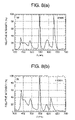
where, To designates a coefficient and is determined mainly by the transmittance of the polarizer used in the liquid crystal panel, θ designates the angle between an effective optical axis in the liquid crystal layer and a transmittance axis for polarized light, d designates the thickness of the liquid crystal layer, Δn designates the anisotropy of the refractive index of the liquid crystal layer, and λ denotes the wavelength of light. Because the transmittance of the liquid crystal display apparatus has essentially a maximum value at a certain wavelength, the liquid crystal display elements are colored. One solution to the above equation is a value which satisfies a condition wherein the peak wavelength becomes equal to the maximum wavelength 555 nm for luminous efficiency under a retardation of 0 order, that is, (πd·Δn/555)=π/2. In this case, the transmittance falls suddenly on the short wavelength side of the peak wavelength, and it decreases gradually on the long wavelength side. Therefore, the liquid crystal display elements are colored yellow. As a result, it is required to use a light source with the color of a cold color family which represents a complementary color to yellow. In other words, it is required to use a light source with a high color-temperature characteristic.
T=T 0·sin2 2θ·sin2 [(π·deff ·Δn)/λ] (2)
where, T0 designates a coefficient and is determined mainly by the transmittance of the polarizer used in the liquid crystal panel, θ designates the angle between an effective optical axis in the liquid crystal layer and a transmittance axis for polarized light, deff designates the thickness of the liquid crystal layer, Δ denotes the anisotropy of the refractive index of the liquid crystal layer, and λ designates the wavelength of light. Further, the product of deff and Δ is referred to as retardation. Here, the thickness deff of the liquid crystal layer is not the thickness of the whole liquid crystal layer, but the thickness of the liquid crystal layer in which the direction of alignment is changed when a voltage is applied.
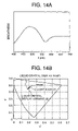
(2) The liquid crystal display panel may be provided with a birefringent film, which is set so as that the peak wavelength of the spectrum transmittance in the liquid crystal display panel can be within the short wavelength range of the visible light of 400 nm to 520 nm, preferably 440 nm to 490 nm.
(3) The liquid crystal display panel may be provided with a color filter. The thickness of the liquid crystal layer at a portion where red light can be transmitted is less than the thickness dLC of the liquid crystal layer at a portion where green light or blue light can be transmitted.
where, dLC designates the thickness of the liquid crystal layer, K2 represents an elastic constant, Δε designates the anisotropy of a dielectric constant of the liquid crystal, and ε denotes a dielectric constant for a vacuum. As dLC is reduced, the threshold voltage shifts to a higher voltage. By setting the thickness of the liquid crystal to be thin at a pixel portion where red is displayed, it becomes possible to shift red, that is, a voltage-transmittance characteristic in a long wavelength region to a higher voltage side. Thereby, the transmittance at the long wavelength region for each voltage is suppressed, and thus it becomes possible to make a liquid crystal display. apparatus in which the transmittance in the short wavelength region is larger. In order to suppress sufficiently the transmittance in the high wavelength region and hold a color balance, it is preferable that the change in thickness of the liquid crystal is suppressed within the range of 0.1 μm to 1 μm. For example, it is possible to reduce dLC by thickening the film at a portion of the color filter where red is displayed. It may be possible to thicken the film at a portion of the color filter where blue is displayed more than dLC at portions where red and green are displayed. Also, in this case, it is preferable that the change in the thickness of the liquid crystal layer is within the range of 0.1 μm to 15 μm.
Claims (10)
Priority Applications (2)
| Application Number | Priority Date | Filing Date | Title |
|---|---|---|---|
| US11/299,699 US7433012B2 (en) | 1995-10-23 | 2005-12-13 | Active matrix type liquid crystal display apparatus |
| US12/244,181 US7684005B2 (en) | 1995-10-23 | 2008-10-02 | Active matrix type liquid crystal display apparatus |
Applications Claiming Priority (8)
| Application Number | Priority Date | Filing Date | Title |
|---|---|---|---|
| JP7273921A JPH09113937A (en) | 1995-10-23 | 1995-10-23 | Liquid crystal display device |
| JP7-273921 | 1995-10-23 | ||
| JP11473996A JP3317846B2 (en) | 1996-05-09 | 1996-05-09 | Liquid crystal display |
| JP8-114739 | 1996-05-09 | ||
| US08/740,008 US6137560A (en) | 1995-10-23 | 1996-10-23 | Active matrix type liquid crystal display apparatus with light source color compensation |
| US09/572,375 US6621538B1 (en) | 1995-10-23 | 2000-05-18 | Active matrix type liquid crystal display apparatus including liquid crystal layer having different thicknesses at portions where different colors of light are transmitted |
| US10/629,711 US7209211B2 (en) | 1995-10-23 | 2003-07-30 | Active matrix type liquid crystal display apparatus |
| US11/299,699 US7433012B2 (en) | 1995-10-23 | 2005-12-13 | Active matrix type liquid crystal display apparatus |
Related Parent Applications (1)
| Application Number | Title | Priority Date | Filing Date |
|---|---|---|---|
| US10/629,711 Continuation US7209211B2 (en) | 1995-10-23 | 2003-07-30 | Active matrix type liquid crystal display apparatus |
Related Child Applications (1)
| Application Number | Title | Priority Date | Filing Date |
|---|---|---|---|
| US12/244,181 Continuation US7684005B2 (en) | 1995-10-23 | 2008-10-02 | Active matrix type liquid crystal display apparatus |
Publications (2)
| Publication Number | Publication Date |
|---|---|
| US20060087482A1 US20060087482A1 (en) | 2006-04-27 |
| US7433012B2 true US7433012B2 (en) | 2008-10-07 |
Family
ID=26453416
Family Applications (5)
| Application Number | Title | Priority Date | Filing Date |
|---|---|---|---|
| US08/740,008 Expired - Lifetime US6137560A (en) | 1995-10-23 | 1996-10-23 | Active matrix type liquid crystal display apparatus with light source color compensation |
| US09/572,375 Expired - Lifetime US6621538B1 (en) | 1995-10-23 | 2000-05-18 | Active matrix type liquid crystal display apparatus including liquid crystal layer having different thicknesses at portions where different colors of light are transmitted |
| US10/629,711 Expired - Fee Related US7209211B2 (en) | 1995-10-23 | 2003-07-30 | Active matrix type liquid crystal display apparatus |
| US11/299,699 Expired - Fee Related US7433012B2 (en) | 1995-10-23 | 2005-12-13 | Active matrix type liquid crystal display apparatus |
| US12/244,181 Expired - Fee Related US7684005B2 (en) | 1995-10-23 | 2008-10-02 | Active matrix type liquid crystal display apparatus |
Family Applications Before (3)
| Application Number | Title | Priority Date | Filing Date |
|---|---|---|---|
| US08/740,008 Expired - Lifetime US6137560A (en) | 1995-10-23 | 1996-10-23 | Active matrix type liquid crystal display apparatus with light source color compensation |
| US09/572,375 Expired - Lifetime US6621538B1 (en) | 1995-10-23 | 2000-05-18 | Active matrix type liquid crystal display apparatus including liquid crystal layer having different thicknesses at portions where different colors of light are transmitted |
| US10/629,711 Expired - Fee Related US7209211B2 (en) | 1995-10-23 | 2003-07-30 | Active matrix type liquid crystal display apparatus |
Family Applications After (1)
| Application Number | Title | Priority Date | Filing Date |
|---|---|---|---|
| US12/244,181 Expired - Fee Related US7684005B2 (en) | 1995-10-23 | 2008-10-02 | Active matrix type liquid crystal display apparatus |
Country Status (2)
| Country | Link |
|---|---|
| US (5) | US6137560A (en) |
| KR (1) | KR100405893B1 (en) |
Cited By (1)
| Publication number | Priority date | Publication date | Assignee | Title |
|---|---|---|---|---|
| US20060158573A1 (en) * | 2005-01-18 | 2006-07-20 | Samsung Electronics Co., Ltd. | Liquid crystal display |
Families Citing this family (37)
| Publication number | Priority date | Publication date | Assignee | Title |
|---|---|---|---|---|
| US6137560A (en) * | 1995-10-23 | 2000-10-24 | Hitachi, Ltd. | Active matrix type liquid crystal display apparatus with light source color compensation |
| US6014190A (en) * | 1995-11-30 | 2000-01-11 | Samsung Electronics Co., Ltd. | In-plane switching liquid crystal display and a manufacturing method thereof |
| EP0785457A3 (en) * | 1996-01-17 | 1998-10-14 | Nippon Telegraph And Telephone Corporation | Optical device and three-dimensional display device |
| CN1100279C (en) * | 1996-10-29 | 2003-01-29 | 日本电气株式会社 | Active matrix liquid crystal display panel |
| JP3788649B2 (en) | 1996-11-22 | 2006-06-21 | 株式会社半導体エネルギー研究所 | Liquid crystal display |
| TW515925B (en) * | 1996-12-25 | 2003-01-01 | Sharp Kk | Liquid crystal display device |
| US7663607B2 (en) | 2004-05-06 | 2010-02-16 | Apple Inc. | Multipoint touchscreen |
| TW569058B (en) * | 1998-02-24 | 2004-01-01 | Toshiba Corp | Array substrate for liquid crystal display element, array substrate for liquid crystal display element and method of manufacturing the same |
| KR100453177B1 (en) * | 1998-09-19 | 2005-04-08 | 엘지.필립스 엘시디 주식회사 | Liquid Crystal Display with Black Layer and Fabricating Method Thereof |
| US7123277B2 (en) * | 2001-05-09 | 2006-10-17 | Clairvoyante, Inc. | Conversion of a sub-pixel format data to another sub-pixel data format |
| KR100759978B1 (en) * | 2001-07-12 | 2007-09-18 | 삼성전자주식회사 | A vertically aligned mode liquid crystal display and a color filter substrate for the same |
| US7417648B2 (en) | 2002-01-07 | 2008-08-26 | Samsung Electronics Co. Ltd., | Color flat panel display sub-pixel arrangements and layouts for sub-pixel rendering with split blue sub-pixels |
| US7755652B2 (en) | 2002-01-07 | 2010-07-13 | Samsung Electronics Co., Ltd. | Color flat panel display sub-pixel rendering and driver configuration for sub-pixel arrangements with split sub-pixels |
| US20040051724A1 (en) | 2002-09-13 | 2004-03-18 | Elliott Candice Hellen Brown | Four color arrangements of emitters for subpixel rendering |
| US7492379B2 (en) | 2002-01-07 | 2009-02-17 | Samsung Electronics Co., Ltd. | Color flat panel display sub-pixel arrangements and layouts for sub-pixel rendering with increased modulation transfer function response |
| US7583279B2 (en) * | 2004-04-09 | 2009-09-01 | Samsung Electronics Co., Ltd. | Subpixel layouts and arrangements for high brightness displays |
| US7598961B2 (en) * | 2003-10-21 | 2009-10-06 | Samsung Electronics Co., Ltd. | method and apparatus for converting from a source color space to a target color space |
| JP2005156752A (en) * | 2003-11-21 | 2005-06-16 | Sony Corp | Liquid crystal display element and projection display device |
| US7248268B2 (en) | 2004-04-09 | 2007-07-24 | Clairvoyante, Inc | Subpixel rendering filters for high brightness subpixel layouts |
| US7301543B2 (en) * | 2004-04-09 | 2007-11-27 | Clairvoyante, Inc. | Systems and methods for selecting a white point for image displays |
| US7619637B2 (en) * | 2004-04-09 | 2009-11-17 | Samsung Electronics Co., Ltd. | Systems and methods for improved gamut mapping from one image data set to another |
| KR101094772B1 (en) * | 2004-06-30 | 2011-12-16 | 엘지디스플레이 주식회사 | Tiled display device |
| CN1882103B (en) * | 2005-04-04 | 2010-06-23 | 三星电子株式会社 | Systems and methods for implementing improved gamut mapping algorithms |
| US7956499B2 (en) * | 2005-06-02 | 2011-06-07 | Seagate Technology Llc | Motor magnetic force attenuator |
| TW200643534A (en) * | 2005-06-07 | 2006-12-16 | Chi Mei Optoelectronics Corp | Liquid crystal display module |
| US7705855B2 (en) * | 2005-06-15 | 2010-04-27 | Samsung Electronics Co., Ltd. | Bichromatic display |
| KR20070059293A (en) * | 2005-12-06 | 2007-06-12 | 삼성전자주식회사 | Liquid crystal display, panel therefor, and manufacturing method thereof |
| US7592996B2 (en) * | 2006-06-02 | 2009-09-22 | Samsung Electronics Co., Ltd. | Multiprimary color display with dynamic gamut mapping |
| EP3805907A1 (en) * | 2006-06-09 | 2021-04-14 | Apple Inc. | Touch screen liquid crystal display |
| US8018476B2 (en) | 2006-08-28 | 2011-09-13 | Samsung Electronics Co., Ltd. | Subpixel layouts for high brightness displays and systems |
| US7876341B2 (en) | 2006-08-28 | 2011-01-25 | Samsung Electronics Co., Ltd. | Subpixel layouts for high brightness displays and systems |
| WO2008039764A2 (en) * | 2006-09-30 | 2008-04-03 | Clairvoyante, Inc. | Systems and methods for reducing desaturation of images rendered on high brightness displays |
| US9710095B2 (en) | 2007-01-05 | 2017-07-18 | Apple Inc. | Touch screen stack-ups |
| JP2010161321A (en) * | 2009-01-09 | 2010-07-22 | Panasonic Corp | Optical device and method of manufacturing the same |
| JP2012078692A (en) * | 2010-10-05 | 2012-04-19 | Hitachi Displays Ltd | Display device |
| US8804056B2 (en) | 2010-12-22 | 2014-08-12 | Apple Inc. | Integrated touch screens |
| JP6459895B2 (en) * | 2015-10-16 | 2019-01-30 | 株式会社デンソー | Liquid crystal display |
Citations (32)
| Publication number | Priority date | Publication date | Assignee | Title |
|---|---|---|---|---|
| US4345249A (en) | 1979-12-25 | 1982-08-17 | Citizen Watch Company Limited | Liquid crystal display panel |
| US4550436A (en) | 1983-07-26 | 1985-10-29 | At&T Bell Laboratories | Parallel text matching methods and apparatus |
| US4632514A (en) | 1984-01-31 | 1986-12-30 | Matsushita Electric Industrial Co., Ltd. | Color liquid crystal display apparatus |
| US4697884A (en) | 1983-07-12 | 1987-10-06 | Bbc Brown, Boveri & Company, Limited | Liquid crystal display having degree of twist and thickness for improved multiplexing |
| JPS6321907A (en) | 1986-06-26 | 1988-01-29 | シニサロ スポルト オサケイフテイオ | Protective clothing |
| JPH0213926A (en) | 1988-07-01 | 1990-01-18 | Canon Inc | Liquid crystal device |
| US4909604A (en) | 1987-08-28 | 1990-03-20 | Hitachi, Ltd. | Light source device |
| US4973137A (en) | 1987-11-04 | 1990-11-27 | Sharp Kabushiki Kaisha | Liquid crystal display device with compensation layers |
| WO1991010936A1 (en) | 1990-01-09 | 1991-07-25 | Fraunhofer-Gesellschaft zur Förderung der angewandten Forschung e.V. | Electro-optical liquid crystal switch element |
| US5048933A (en) | 1989-04-14 | 1991-09-17 | Konica Corporation | Transmission type liquid crystal display device |
| JPH03233518A (en) | 1990-02-09 | 1991-10-17 | Seiko Epson Corp | Liquid crystal display device |
| US5089906A (en) | 1989-02-06 | 1992-02-18 | Sharp Kabushiki Kaisha | Supertwisted nematic liquid crystal device having two phase difference plates for providing black/white display |
| JPH0457011A (en) | 1990-06-27 | 1992-02-24 | Sanyo Electric Co Ltd | Miniature display device |
| US5119216A (en) | 1987-12-10 | 1992-06-02 | Seiko Epson Corporation | Electro-optical device |
| US5124825A (en) | 1988-05-02 | 1992-06-23 | Konica Corporation | Liquid crystal display device |
| JPH04181219A (en) | 1990-11-16 | 1992-06-29 | Canon Inc | Ferroelectric liquid crystal element |
| USRE33987E (en) | 1980-03-24 | 1992-07-07 | Seiko Epson Corporation | Backlighted liquid crystal display |
| US5130834A (en) | 1988-02-19 | 1992-07-14 | Alps Electric Co., Ltd. | Liquid crystal display including a dye complementary to the liquid crystal's bright state color |
| US5132825A (en) | 1989-10-18 | 1992-07-21 | Asahi Kogaku Kogyo Kabushiki Kaisha | Image processing apparatus having control means for adjusting the color temperature of the displayed image |
| US5139340A (en) | 1989-12-08 | 1992-08-18 | Seiko Epson Corporation | Single polarizer, reflective type liquid crystal display device with high brightness and contrast ratio |
| US5211463A (en) | 1992-03-11 | 1993-05-18 | Kaiser Aerospace & Electronics Corporation | Backlight for liquid crystal devices |
| JPH06222397A (en) | 1993-01-25 | 1994-08-12 | Sony Corp | Liquid crystal display device |
| JPH0868997A (en) | 1994-08-30 | 1996-03-12 | Hitachi Ltd | Liquid crystal display device |
| JPH0882715A (en) | 1994-09-13 | 1996-03-26 | Hitachi Ltd | Liquid crystal display device |
| JPH0894848A (en) | 1994-09-28 | 1996-04-12 | Kyocera Corp | Liquid crystal display device |
| JPH0895015A (en) | 1994-09-27 | 1996-04-12 | Nippon Sheet Glass Co Ltd | Liquid crystal display device |
| JPH08106010A (en) | 1994-10-04 | 1996-04-23 | Sony Corp | Liquid crystal display device |
| US5532854A (en) | 1994-01-25 | 1996-07-02 | Fergason; James L. | Folded variable birefringerence zeroth order hybrid aligned liquid crystal apparatus |
| US5541750A (en) | 1990-12-13 | 1996-07-30 | Samsung Electron Devices Co., Ltd. | Color filter for a liquid crystal display using at least one of acid red 52, acid red 486, and rhodamine 6 GCT |
| US5745200A (en) | 1994-04-28 | 1998-04-28 | Casio Computer Co., Ltd. | Color liquid crystal display device and liquid crystal display apparatus |
| US5757524A (en) | 1994-04-12 | 1998-05-26 | Rockwell International | Normally white multigap twisted nematic liquid crystal display with reduced hue variation over viewing angle |
| US5841498A (en) | 1990-01-09 | 1998-11-24 | Merck Patent Gesellschaft Mit Beschrankter Haftung | Liquid crystal display devices having a parallel electric field and βO, which is not 0 degrees or 90 degrees |
Family Cites Families (7)
| Publication number | Priority date | Publication date | Assignee | Title |
|---|---|---|---|---|
| US33987A (en) * | 1861-12-24 | Improvement in refining and crystallizing sugar | ||
| US5302946A (en) * | 1988-07-21 | 1994-04-12 | Leonid Shapiro | Stacked display panel construction and method of making same |
| EP0916992B1 (en) * | 1992-09-18 | 2003-11-26 | Hitachi, Ltd. | A liquid crystal display device |
| JPH06165189A (en) * | 1992-11-25 | 1994-06-10 | Nikon Corp | White balance adjusting device |
| JP3233518B2 (en) | 1993-11-24 | 2001-11-26 | タカタ株式会社 | Seat belt retractor |
| US6137560A (en) * | 1995-10-23 | 2000-10-24 | Hitachi, Ltd. | Active matrix type liquid crystal display apparatus with light source color compensation |
| DE19624154A1 (en) | 1996-06-18 | 1998-01-08 | Hoechst Ag | Ring-fused dihydropyrans, process for their preparation and their use |
-
1996
- 1996-10-23 US US08/740,008 patent/US6137560A/en not_active Expired - Lifetime
- 1996-10-23 KR KR1019960047591A patent/KR100405893B1/en not_active IP Right Cessation
-
2000
- 2000-05-18 US US09/572,375 patent/US6621538B1/en not_active Expired - Lifetime
-
2003
- 2003-07-30 US US10/629,711 patent/US7209211B2/en not_active Expired - Fee Related
-
2005
- 2005-12-13 US US11/299,699 patent/US7433012B2/en not_active Expired - Fee Related
-
2008
- 2008-10-02 US US12/244,181 patent/US7684005B2/en not_active Expired - Fee Related
Patent Citations (34)
| Publication number | Priority date | Publication date | Assignee | Title |
|---|---|---|---|---|
| US4345249A (en) | 1979-12-25 | 1982-08-17 | Citizen Watch Company Limited | Liquid crystal display panel |
| USRE33987E (en) | 1980-03-24 | 1992-07-07 | Seiko Epson Corporation | Backlighted liquid crystal display |
| US4697884A (en) | 1983-07-12 | 1987-10-06 | Bbc Brown, Boveri & Company, Limited | Liquid crystal display having degree of twist and thickness for improved multiplexing |
| US4697884B1 (en) | 1983-07-12 | 1990-08-28 | Bbc Brown Boveri & Cie | |
| US4550436A (en) | 1983-07-26 | 1985-10-29 | At&T Bell Laboratories | Parallel text matching methods and apparatus |
| US4632514A (en) | 1984-01-31 | 1986-12-30 | Matsushita Electric Industrial Co., Ltd. | Color liquid crystal display apparatus |
| JPS6321907A (en) | 1986-06-26 | 1988-01-29 | シニサロ スポルト オサケイフテイオ | Protective clothing |
| US4909604A (en) | 1987-08-28 | 1990-03-20 | Hitachi, Ltd. | Light source device |
| US4973137A (en) | 1987-11-04 | 1990-11-27 | Sharp Kabushiki Kaisha | Liquid crystal display device with compensation layers |
| US5119216A (en) | 1987-12-10 | 1992-06-02 | Seiko Epson Corporation | Electro-optical device |
| US5130834A (en) | 1988-02-19 | 1992-07-14 | Alps Electric Co., Ltd. | Liquid crystal display including a dye complementary to the liquid crystal's bright state color |
| US5124825A (en) | 1988-05-02 | 1992-06-23 | Konica Corporation | Liquid crystal display device |
| JPH0213926A (en) | 1988-07-01 | 1990-01-18 | Canon Inc | Liquid crystal device |
| US5414542A (en) | 1988-07-01 | 1995-05-09 | Canon Kabushiki Kaisha | Liquid crystal apparatus |
| US5089906A (en) | 1989-02-06 | 1992-02-18 | Sharp Kabushiki Kaisha | Supertwisted nematic liquid crystal device having two phase difference plates for providing black/white display |
| US5048933A (en) | 1989-04-14 | 1991-09-17 | Konica Corporation | Transmission type liquid crystal display device |
| US5132825A (en) | 1989-10-18 | 1992-07-21 | Asahi Kogaku Kogyo Kabushiki Kaisha | Image processing apparatus having control means for adjusting the color temperature of the displayed image |
| US5139340A (en) | 1989-12-08 | 1992-08-18 | Seiko Epson Corporation | Single polarizer, reflective type liquid crystal display device with high brightness and contrast ratio |
| WO1991010936A1 (en) | 1990-01-09 | 1991-07-25 | Fraunhofer-Gesellschaft zur Förderung der angewandten Forschung e.V. | Electro-optical liquid crystal switch element |
| US5841498A (en) | 1990-01-09 | 1998-11-24 | Merck Patent Gesellschaft Mit Beschrankter Haftung | Liquid crystal display devices having a parallel electric field and βO, which is not 0 degrees or 90 degrees |
| JPH03233518A (en) | 1990-02-09 | 1991-10-17 | Seiko Epson Corp | Liquid crystal display device |
| JPH0457011A (en) | 1990-06-27 | 1992-02-24 | Sanyo Electric Co Ltd | Miniature display device |
| JPH04181219A (en) | 1990-11-16 | 1992-06-29 | Canon Inc | Ferroelectric liquid crystal element |
| US5541750A (en) | 1990-12-13 | 1996-07-30 | Samsung Electron Devices Co., Ltd. | Color filter for a liquid crystal display using at least one of acid red 52, acid red 486, and rhodamine 6 GCT |
| US5211463A (en) | 1992-03-11 | 1993-05-18 | Kaiser Aerospace & Electronics Corporation | Backlight for liquid crystal devices |
| JPH06222397A (en) | 1993-01-25 | 1994-08-12 | Sony Corp | Liquid crystal display device |
| US5532854A (en) | 1994-01-25 | 1996-07-02 | Fergason; James L. | Folded variable birefringerence zeroth order hybrid aligned liquid crystal apparatus |
| US5757524A (en) | 1994-04-12 | 1998-05-26 | Rockwell International | Normally white multigap twisted nematic liquid crystal display with reduced hue variation over viewing angle |
| US5745200A (en) | 1994-04-28 | 1998-04-28 | Casio Computer Co., Ltd. | Color liquid crystal display device and liquid crystal display apparatus |
| JPH0868997A (en) | 1994-08-30 | 1996-03-12 | Hitachi Ltd | Liquid crystal display device |
| JPH0882715A (en) | 1994-09-13 | 1996-03-26 | Hitachi Ltd | Liquid crystal display device |
| JPH0895015A (en) | 1994-09-27 | 1996-04-12 | Nippon Sheet Glass Co Ltd | Liquid crystal display device |
| JPH0894848A (en) | 1994-09-28 | 1996-04-12 | Kyocera Corp | Liquid crystal display device |
| JPH08106010A (en) | 1994-10-04 | 1996-04-23 | Sony Corp | Liquid crystal display device |
Non-Patent Citations (6)
| Title |
|---|
| Electronic Display Devices, Masumotot et al., 1990, pp. 70-72. * |
| Liquid crystal applications and uses, vol. 1, pp. 188-194, 261-267, 1990, Bahadur. * |
| Nitta et al High Quality Super-IPS LCD System For Moving Picture, AM-LCD '03 pp. 253-256 ; 2003. |
| Utsumi et al "Development of Authentic-Color IPS LCD without Color Tracking", SID 02 Digest, pp. 820-823; 2002. |
| Utsumi, "Color Tracking In Relation To Liquid Crystal Display Characteristics", Asia Display IDS '01 pp. 117-120; 2001. |
| Utsumi, "Improving Color Tracking In In-Plane Switching Mode Liquid-Crystal Displays", MRS Bulletin. Nov. 2002, pp. 1-4. |
Cited By (2)
| Publication number | Priority date | Publication date | Assignee | Title |
|---|---|---|---|---|
| US20060158573A1 (en) * | 2005-01-18 | 2006-07-20 | Samsung Electronics Co., Ltd. | Liquid crystal display |
| US7768582B2 (en) * | 2005-01-18 | 2010-08-03 | Samsung Electronics Co., Ltd. | Liquid crystal display |
Also Published As
| Publication number | Publication date |
|---|---|
| US20060087482A1 (en) | 2006-04-27 |
| US6137560A (en) | 2000-10-24 |
| US20040021818A1 (en) | 2004-02-05 |
| US7209211B2 (en) | 2007-04-24 |
| US7684005B2 (en) | 2010-03-23 |
| US20090040438A1 (en) | 2009-02-12 |
| KR100405893B1 (en) | 2004-10-06 |
| US6621538B1 (en) | 2003-09-16 |
| KR970022450A (en) | 1997-05-28 |
Similar Documents
| Publication | Publication Date | Title |
|---|---|---|
| US7433012B2 (en) | Active matrix type liquid crystal display apparatus | |
| JP3362758B2 (en) | Reflective color display | |
| US7623202B2 (en) | Liquid crystal display device | |
| US7554516B2 (en) | Display device and method for driving the same | |
| US20040145691A1 (en) | Transflective liquid crystal display device | |
| JP4303906B2 (en) | Transflective liquid crystal display device | |
| KR20010109333A (en) | Liquid-crystal display | |
| US8767137B2 (en) | Liquid crystal display device with red, green and blue subpixels having different aperture ratios | |
| JP3893533B2 (en) | Liquid crystal display | |
| JP2000187231A (en) | Liquid crystal display device | |
| JP2000356768A (en) | Color filter and liquid crystal display device | |
| JP3317846B2 (en) | Liquid crystal display | |
| JPH0330126B2 (en) | ||
| JPH09113937A (en) | Liquid crystal display device | |
| JP3849708B2 (en) | Liquid crystal display | |
| JP2819602B2 (en) | Liquid crystal display device | |
| JP3716857B2 (en) | Liquid crystal display device | |
| JP2947801B2 (en) | Nematic liquid crystal display device with twisted helical structure | |
| JP2001108957A (en) | Liquid crystal display device | |
| JP2001183665A (en) | Liquid crystal display device | |
| JP2004280129A (en) | Liquid crystal display device | |
| JP2002082332A (en) | Liquid crystal display | |
| KR19980033100A (en) | Guest Host Type Liquid Crystal Composition | |
| JPH11109332A (en) | Liquid crystal display device | |
| JPH08248449A (en) | Liquid crystal display device |
Legal Events
| Date | Code | Title | Description |
|---|---|---|---|
| STCF | Information on status: patent grant |
Free format text: PATENTED CASE |
|
| FEPP | Fee payment procedure |
Free format text: PAYOR NUMBER ASSIGNED (ORIGINAL EVENT CODE: ASPN); ENTITY STATUS OF PATENT OWNER: LARGE ENTITY |
|
| AS | Assignment |
Owner name: PANASONIC LIQUID CRYSTAL DISPLAY CO., LTD., JAPAN Free format text: MERGER/CHANGE OF NAME;ASSIGNOR:IPS ALPHA SUPPORT CO., LTD.;REEL/FRAME:027363/0315 Effective date: 20101001 Owner name: HITACHI DISPLAYS, LTD., JAPAN Free format text: COMPANY SPLIT PLAN TRANSFERRING ONE HUNDRED (100) PERCENT SHARE OF PATENT AND PATENT APPLICATIONS;ASSIGNOR:HITACHI, LTD.;REEL/FRAME:027362/0612 Effective date: 20021001 Owner name: IPS ALPHA SUPPORT CO., LTD., JAPAN Free format text: COMPANY SPLIT PLAN TRANSFERRING FIFTY (50) PERCENT SHARE OF PATENTS AND PATENT APPLICATIONS;ASSIGNOR:HITACHI DISPLAYS, LTD.;REEL/FRAME:027362/0466 Effective date: 20100630 |
|
| FPAY | Fee payment |
Year of fee payment: 4 |
|
| FPAY | Fee payment |
Year of fee payment: 8 |
|
| FEPP | Fee payment procedure |
Free format text: MAINTENANCE FEE REMINDER MAILED (ORIGINAL EVENT CODE: REM.); ENTITY STATUS OF PATENT OWNER: LARGE ENTITY |
|
| LAPS | Lapse for failure to pay maintenance fees |
Free format text: PATENT EXPIRED FOR FAILURE TO PAY MAINTENANCE FEES (ORIGINAL EVENT CODE: EXP.); ENTITY STATUS OF PATENT OWNER: LARGE ENTITY |
|
| STCH | Information on status: patent discontinuation |
Free format text: PATENT EXPIRED DUE TO NONPAYMENT OF MAINTENANCE FEES UNDER 37 CFR 1.362 |
|
| FP | Lapsed due to failure to pay maintenance fee |
Effective date: 20201007 |