US7566853B2 - Image sensor employing a plurality of photodetector arrays and/or rear-illuminated architecture - Google Patents
Image sensor employing a plurality of photodetector arrays and/or rear-illuminated architecture Download PDFInfo
- Publication number
- US7566853B2 US7566853B2 US11/317,207 US31720705A US7566853B2 US 7566853 B2 US7566853 B2 US 7566853B2 US 31720705 A US31720705 A US 31720705A US 7566853 B2 US7566853 B2 US 7566853B2
- Authority
- US
- United States
- Prior art keywords
- photodetectors
- arrays
- sensor
- contiguous
- light
- Prior art date
- Legal status (The legal status is an assumption and is not a legal conclusion. Google has not performed a legal analysis and makes no representation as to the accuracy of the status listed.)
- Active, expires
Links
- 238000003491 array Methods 0.000 title claims abstract description 98
- 239000000758 substrate Substances 0.000 claims abstract description 22
- 239000000463 material Substances 0.000 claims description 20
- 239000004065 semiconductor Substances 0.000 claims description 14
- 230000005540 biological transmission Effects 0.000 claims description 7
- 238000004891 communication Methods 0.000 claims description 7
- 230000009365 direct transmission Effects 0.000 claims description 5
- VYPSYNLAJGMNEJ-UHFFFAOYSA-N Silicium dioxide Chemical compound O=[Si]=O VYPSYNLAJGMNEJ-UHFFFAOYSA-N 0.000 claims description 4
- LIVNPJMFVYWSIS-UHFFFAOYSA-N silicon monoxide Chemical class [Si-]#[O+] LIVNPJMFVYWSIS-UHFFFAOYSA-N 0.000 claims description 4
- 229910052814 silicon oxide Inorganic materials 0.000 claims description 4
- PNEYBMLMFCGWSK-UHFFFAOYSA-N Alumina Chemical class [O-2].[O-2].[O-2].[Al+3].[Al+3] PNEYBMLMFCGWSK-UHFFFAOYSA-N 0.000 claims description 3
- 229910021419 crystalline silicon Inorganic materials 0.000 claims 1
- 238000004377 microelectronic Methods 0.000 description 13
- 229910000679 solder Inorganic materials 0.000 description 11
- 230000003287 optical effect Effects 0.000 description 10
- 230000008901 benefit Effects 0.000 description 9
- 238000005516 engineering process Methods 0.000 description 9
- 239000003086 colorant Substances 0.000 description 8
- 238000000034 method Methods 0.000 description 8
- 229910052710 silicon Inorganic materials 0.000 description 8
- XUIMIQQOPSSXEZ-UHFFFAOYSA-N Silicon Chemical compound [Si] XUIMIQQOPSSXEZ-UHFFFAOYSA-N 0.000 description 7
- 229920000642 polymer Polymers 0.000 description 7
- 239000010703 silicon Substances 0.000 description 7
- 230000007246 mechanism Effects 0.000 description 6
- 235000012431 wafers Nutrition 0.000 description 6
- 229910010293 ceramic material Inorganic materials 0.000 description 5
- 239000011521 glass Substances 0.000 description 5
- 238000004519 manufacturing process Methods 0.000 description 5
- 238000003384 imaging method Methods 0.000 description 4
- 230000035945 sensitivity Effects 0.000 description 4
- 239000012212 insulator Substances 0.000 description 3
- 239000011159 matrix material Substances 0.000 description 3
- 238000004806 packaging method and process Methods 0.000 description 3
- 230000035515 penetration Effects 0.000 description 3
- -1 polyethylene terephthalates Polymers 0.000 description 3
- 230000008569 process Effects 0.000 description 3
- 238000012545 processing Methods 0.000 description 3
- 230000001681 protective effect Effects 0.000 description 3
- 239000010453 quartz Substances 0.000 description 3
- 241001326510 Phacelia sericea Species 0.000 description 2
- 206010034960 Photophobia Diseases 0.000 description 2
- 230000002238 attenuated effect Effects 0.000 description 2
- 238000000576 coating method Methods 0.000 description 2
- 150000001875 compounds Chemical class 0.000 description 2
- 229920001577 copolymer Polymers 0.000 description 2
- 239000000428 dust Substances 0.000 description 2
- 230000004907 flux Effects 0.000 description 2
- 238000010348 incorporation Methods 0.000 description 2
- 208000013469 light sensitivity Diseases 0.000 description 2
- 238000012536 packaging technology Methods 0.000 description 2
- 230000000149 penetrating effect Effects 0.000 description 2
- 229920000412 polyarylene Polymers 0.000 description 2
- 229910052594 sapphire Inorganic materials 0.000 description 2
- 239000010980 sapphire Substances 0.000 description 2
- 239000007787 solid Substances 0.000 description 2
- 238000005382 thermal cycling Methods 0.000 description 2
- 229910001218 Gallium arsenide Inorganic materials 0.000 description 1
- 239000002033 PVDF binder Substances 0.000 description 1
- 239000004642 Polyimide Substances 0.000 description 1
- 239000004793 Polystyrene Substances 0.000 description 1
- 229920001328 Polyvinylidene chloride Polymers 0.000 description 1
- ATJFFYVFTNAWJD-UHFFFAOYSA-N Tin Chemical compound [Sn] ATJFFYVFTNAWJD-UHFFFAOYSA-N 0.000 description 1
- QCWXUUIWCKQGHC-UHFFFAOYSA-N Zirconium Chemical compound [Zr] QCWXUUIWCKQGHC-UHFFFAOYSA-N 0.000 description 1
- 230000004075 alteration Effects 0.000 description 1
- 229910052782 aluminium Inorganic materials 0.000 description 1
- XAGFODPZIPBFFR-UHFFFAOYSA-N aluminium Chemical compound [Al] XAGFODPZIPBFFR-UHFFFAOYSA-N 0.000 description 1
- 230000003667 anti-reflective effect Effects 0.000 description 1
- 230000000903 blocking effect Effects 0.000 description 1
- 230000001413 cellular effect Effects 0.000 description 1
- 239000000919 ceramic Substances 0.000 description 1
- 239000011248 coating agent Substances 0.000 description 1
- 230000000295 complement effect Effects 0.000 description 1
- 230000001010 compromised effect Effects 0.000 description 1
- 239000004020 conductor Substances 0.000 description 1
- 239000000470 constituent Substances 0.000 description 1
- 238000005314 correlation function Methods 0.000 description 1
- 238000005260 corrosion Methods 0.000 description 1
- 230000007797 corrosion Effects 0.000 description 1
- 239000002178 crystalline material Substances 0.000 description 1
- 125000004122 cyclic group Chemical group 0.000 description 1
- 229920005565 cyclic polymer Polymers 0.000 description 1
- 230000007423 decrease Effects 0.000 description 1
- 238000001514 detection method Methods 0.000 description 1
- 239000003989 dielectric material Substances 0.000 description 1
- 238000009792 diffusion process Methods 0.000 description 1
- 239000002019 doping agent Substances 0.000 description 1
- 150000002170 ethers Chemical class 0.000 description 1
- 230000005496 eutectics Effects 0.000 description 1
- 229910000743 fusible alloy Inorganic materials 0.000 description 1
- 238000010438 heat treatment Methods 0.000 description 1
- 229920001519 homopolymer Polymers 0.000 description 1
- 238000002347 injection Methods 0.000 description 1
- 239000007924 injection Substances 0.000 description 1
- 150000002484 inorganic compounds Chemical class 0.000 description 1
- 229910010272 inorganic material Inorganic materials 0.000 description 1
- 239000011810 insulating material Substances 0.000 description 1
- 230000000670 limiting effect Effects 0.000 description 1
- 238000001459 lithography Methods 0.000 description 1
- 230000013011 mating Effects 0.000 description 1
- 229910052751 metal Inorganic materials 0.000 description 1
- 239000002184 metal Substances 0.000 description 1
- 150000001247 metal acetylides Chemical class 0.000 description 1
- 229910044991 metal oxide Inorganic materials 0.000 description 1
- 150000004706 metal oxides Chemical class 0.000 description 1
- 229910003455 mixed metal oxide Inorganic materials 0.000 description 1
- 238000012986 modification Methods 0.000 description 1
- 230000004048 modification Effects 0.000 description 1
- 150000004767 nitrides Chemical class 0.000 description 1
- 239000011368 organic material Substances 0.000 description 1
- 230000003647 oxidation Effects 0.000 description 1
- 238000007254 oxidation reaction Methods 0.000 description 1
- 229920000052 poly(p-xylylene) Polymers 0.000 description 1
- 229920000515 polycarbonate Polymers 0.000 description 1
- 239000004417 polycarbonate Substances 0.000 description 1
- 229920000139 polyethylene terephthalate Polymers 0.000 description 1
- 229920001721 polyimide Polymers 0.000 description 1
- 229920002223 polystyrene Polymers 0.000 description 1
- 229920001343 polytetrafluoroethylene Polymers 0.000 description 1
- 239000004810 polytetrafluoroethylene Substances 0.000 description 1
- 239000004800 polyvinyl chloride Substances 0.000 description 1
- 229920000915 polyvinyl chloride Polymers 0.000 description 1
- 229920002620 polyvinyl fluoride Polymers 0.000 description 1
- 239000005033 polyvinylidene chloride Substances 0.000 description 1
- 229920002981 polyvinylidene fluoride Polymers 0.000 description 1
- 230000005855 radiation Effects 0.000 description 1
- 230000008707 rearrangement Effects 0.000 description 1
- 230000009467 reduction Effects 0.000 description 1
- 230000002829 reductive effect Effects 0.000 description 1
- 239000000126 substance Substances 0.000 description 1
- 238000010897 surface acoustic wave method Methods 0.000 description 1
- 230000002277 temperature effect Effects 0.000 description 1
- 229910001928 zirconium oxide Inorganic materials 0.000 description 1
Images


Classifications
-
- H—ELECTRICITY
- H01—ELECTRIC ELEMENTS
- H01L—SEMICONDUCTOR DEVICES NOT COVERED BY CLASS H10
- H01L27/00—Devices consisting of a plurality of semiconductor or other solid-state components formed in or on a common substrate
- H01L27/14—Devices consisting of a plurality of semiconductor or other solid-state components formed in or on a common substrate including semiconductor components sensitive to infrared radiation, light, electromagnetic radiation of shorter wavelength or corpuscular radiation and specially adapted either for the conversion of the energy of such radiation into electrical energy or for the control of electrical energy by such radiation
- H01L27/144—Devices controlled by radiation
- H01L27/146—Imager structures
- H01L27/14601—Structural or functional details thereof
- H01L27/14618—Containers
-
- H—ELECTRICITY
- H04—ELECTRIC COMMUNICATION TECHNIQUE
- H04N—PICTORIAL COMMUNICATION, e.g. TELEVISION
- H04N23/00—Cameras or camera modules comprising electronic image sensors; Control thereof
- H04N23/57—Mechanical or electrical details of cameras or camera modules specially adapted for being embedded in other devices
-
- H—ELECTRICITY
- H01—ELECTRIC ELEMENTS
- H01L—SEMICONDUCTOR DEVICES NOT COVERED BY CLASS H10
- H01L27/00—Devices consisting of a plurality of semiconductor or other solid-state components formed in or on a common substrate
- H01L27/14—Devices consisting of a plurality of semiconductor or other solid-state components formed in or on a common substrate including semiconductor components sensitive to infrared radiation, light, electromagnetic radiation of shorter wavelength or corpuscular radiation and specially adapted either for the conversion of the energy of such radiation into electrical energy or for the control of electrical energy by such radiation
- H01L27/144—Devices controlled by radiation
- H01L27/146—Imager structures
- H01L27/14601—Structural or functional details thereof
- H01L27/1462—Coatings
- H01L27/14621—Colour filter arrangements
-
- H—ELECTRICITY
- H01—ELECTRIC ELEMENTS
- H01L—SEMICONDUCTOR DEVICES NOT COVERED BY CLASS H10
- H01L27/00—Devices consisting of a plurality of semiconductor or other solid-state components formed in or on a common substrate
- H01L27/14—Devices consisting of a plurality of semiconductor or other solid-state components formed in or on a common substrate including semiconductor components sensitive to infrared radiation, light, electromagnetic radiation of shorter wavelength or corpuscular radiation and specially adapted either for the conversion of the energy of such radiation into electrical energy or for the control of electrical energy by such radiation
- H01L27/144—Devices controlled by radiation
- H01L27/146—Imager structures
- H01L27/14601—Structural or functional details thereof
- H01L27/14632—Wafer-level processed structures
-
- H—ELECTRICITY
- H04—ELECTRIC COMMUNICATION TECHNIQUE
- H04N—PICTORIAL COMMUNICATION, e.g. TELEVISION
- H04N23/00—Cameras or camera modules comprising electronic image sensors; Control thereof
- H04N23/10—Cameras or camera modules comprising electronic image sensors; Control thereof for generating image signals from different wavelengths
- H04N23/13—Cameras or camera modules comprising electronic image sensors; Control thereof for generating image signals from different wavelengths with multiple sensors
-
- H—ELECTRICITY
- H04—ELECTRIC COMMUNICATION TECHNIQUE
- H04N—PICTORIAL COMMUNICATION, e.g. TELEVISION
- H04N25/00—Circuitry of solid-state image sensors [SSIS]; Control thereof
- H04N25/10—Circuitry of solid-state image sensors [SSIS]; Control thereof for transforming different wavelengths into image signals
- H04N25/11—Arrangement of colour filter arrays [CFA]; Filter mosaics
- H04N25/13—Arrangement of colour filter arrays [CFA]; Filter mosaics characterised by the spectral characteristics of the filter elements
- H04N25/133—Arrangement of colour filter arrays [CFA]; Filter mosaics characterised by the spectral characteristics of the filter elements including elements passing panchromatic light, e.g. filters passing white light
-
- H—ELECTRICITY
- H04—ELECTRIC COMMUNICATION TECHNIQUE
- H04N—PICTORIAL COMMUNICATION, e.g. TELEVISION
- H04N25/00—Circuitry of solid-state image sensors [SSIS]; Control thereof
- H04N25/10—Circuitry of solid-state image sensors [SSIS]; Control thereof for transforming different wavelengths into image signals
- H04N25/11—Arrangement of colour filter arrays [CFA]; Filter mosaics
- H04N25/13—Arrangement of colour filter arrays [CFA]; Filter mosaics characterised by the spectral characteristics of the filter elements
- H04N25/134—Arrangement of colour filter arrays [CFA]; Filter mosaics characterised by the spectral characteristics of the filter elements based on three different wavelength filter elements
-
- H—ELECTRICITY
- H04—ELECTRIC COMMUNICATION TECHNIQUE
- H04N—PICTORIAL COMMUNICATION, e.g. TELEVISION
- H04N25/00—Circuitry of solid-state image sensors [SSIS]; Control thereof
- H04N25/10—Circuitry of solid-state image sensors [SSIS]; Control thereof for transforming different wavelengths into image signals
- H04N25/11—Arrangement of colour filter arrays [CFA]; Filter mosaics
- H04N25/13—Arrangement of colour filter arrays [CFA]; Filter mosaics characterised by the spectral characteristics of the filter elements
- H04N25/135—Arrangement of colour filter arrays [CFA]; Filter mosaics characterised by the spectral characteristics of the filter elements based on four or more different wavelength filter elements
-
- H—ELECTRICITY
- H04—ELECTRIC COMMUNICATION TECHNIQUE
- H04N—PICTORIAL COMMUNICATION, e.g. TELEVISION
- H04N25/00—Circuitry of solid-state image sensors [SSIS]; Control thereof
- H04N25/40—Extracting pixel data from image sensors by controlling scanning circuits, e.g. by modifying the number of pixels sampled or to be sampled
- H04N25/41—Extracting pixel data from a plurality of image sensors simultaneously picking up an image, e.g. for increasing the field of view by combining the outputs of a plurality of sensors
-
- H—ELECTRICITY
- H01—ELECTRIC ELEMENTS
- H01L—SEMICONDUCTOR DEVICES NOT COVERED BY CLASS H10
- H01L2924/00—Indexing scheme for arrangements or methods for connecting or disconnecting semiconductor or solid-state bodies as covered by H01L24/00
- H01L2924/0001—Technical content checked by a classifier
- H01L2924/0002—Not covered by any one of groups H01L24/00, H01L24/00 and H01L2224/00
Definitions
- the invention relates generally to images sensors.
- the invention relates to image sensors that employ a rear-illuminated architecture and/or a plurality of contiguous photodetector arrays.
- image sensor packages are also provided.
- Microelectronic devices such as semiconductor chips are flat bodies having opposing front and rear surfaces. Contacts on either or both surfaces are typically connected to the internal electrical circuitry of the chip itself. Microelectronic devices have become ubiquitous in various consumer product markets, portable or otherwise, due to their size and functionality. For example, microelectronic devices have been employed in optical and imaging applications.
- CMOS complementary metal-oxide semiconductors
- CCD charge-coupled device
- image sensing microelectronic devices are typically illuminated from their front surface, e.g., the front surface of an image sensing chip.
- FIG. 1 schematically depicts a known image sensor architecture for a CCD camera.
- a microelectronic device 10 is provided having parallel opposing front and rear surface, indicated at 12 and 14 , respectively.
- An array of photodetectors 22 is provided on the front surface 12 .
- Each photodetector 22 may be associated with a microlens 30 to improve its sensitivity.
- color filters 40 that allow for the selective transmission of light of a particular wavelength toward the photodetectors 22 .
- a camera lens 50 is placed over the array at a distance selected according to the area of the photodetector array and the focal length of the lens.
- the image sensor architecture depicted in FIG. 1 is known as a front-illuminated architecture.
- microlenses are typically formed from a polymeric material onto which dust and other particular matter may adhere. Once such matter adheres to a microlens, the performance of the photodetector associated therewith is compromised. Thus, such sensors must be handled in a substantially dust-free environment (e.g., a cleanroom) when the microlenses are exposed. Only after the microlenses are protected can an image sensor be removed from the substantially dust-free environment.
- a substantially dust-free environment e.g., a cleanroom
- microelectronic devices may require a protective element, e.g., a cover over all or part of the front surface.
- a protective element e.g., a cover over all or part of the front surface.
- certain electro-optical chips such as optical sensing chips and light-emitting chips have photosensitive elements which must be protected by a cover.
- a cavity may be formed between the protective element and the front device surface.
- Other chips requiring a protective element include, for example, surface acoustic wave or “SAW” chips, microelectromechanical systems or “MEMS” chips (see, e.g., U.S. Pat. No. 5,610,431 to Martin), and chips that employ voltage controlled oscillators (VCOs).
- SAW surface acoustic wave
- MEMS microelectromechanical systems
- VCOs voltage controlled oscillators
- optical devices such as image sensors can be made in the form of a unitary wafer, optionally undergo wafer-scale packaging, and be severed to form individual units. This may be done to improve productivity and reduce costs associated with microelectronic manufacturing.
- the capped chips have electrical interconnects made from elements that extend from contacts of a chip at least partially through a plurality of through holes of a cap.
- the electrical interconnects may be solid, so as to form seals extending across the through holes.
- stud bumps extend from the contacts, forming parts of the electrical interconnects.
- a fusible conductive medium forms a part of the electrical interconnects.
- rear-illuminated architectures may be advantageously employed to overcome the drawbacks of known image sensor technologies.
- architectures employing a plurality of contiguous photodetector arrays may also be advantageously used in conjunction with or as an alternative to rear-illuminated architectures.
- a sensor in a first embodiment, includes an optically transparent substrate having first and second opposing surfaces, a detector layer in contact with the second surface, a plurality of photodetectors, and one or more color filters.
- the first surface is a light-receiving surface.
- the photodetectors are located at sites of first, second, and third arrays in the detector layer.
- the one or more color filters are positioned to allow for selective transmission of light of first, second, and third wavelengths through the substrate to first, second, and third arrays, respectively.
- This embodiment is particularly suited for a sensor architecture that does not employ any microlenses.
- an image sensor comprising a detector layer, first, second, and third arrays of photodetectors, and first, second, and third lenses.
- the arrays are each contiguous, located in the detector layer, and substantially coplanar to each other.
- the lenses are effective to direct transmission of light to their respective photodetector arrays.
- an image sensor comprising a detector layer containing first, second, and third contiguous arrays of photodetectors therein and having a light-receiving surface.
- the arrays are located in the layer at increasing distances from the light-receiving surface. In addition, at least a portion of each array does not overlap another.
- the substrate when used, is typically made from an insulating material.
- a ceramic material may be used.
- exemplary suitable ceramic materials include oxides such as silicon oxides and aluminum oxides. Such oxides may be single crystalline, multicrystalline, or amorphous.
- detectors of the invention are typically located in a detector layer comprising a semiconductor material. While the semiconductor material may consist of or comprise Si, other semiconductor materials may be used as well.
- different embodiments of the invention may have different arrangements of photodetectors.
- the photodetectors are arranged in at least one array.
- any number of photodetector arrays may be used.
- optimal sensor performance may result when arrays are provided in a nonzero positive integer multiples of three, four, or five.
- the arrays may be contiguous or noncontiguous, coplanar or noncoplanar.
- any sensor that employs a plurality of arrays may involve the arrangement of the arrays in a linear pattern.
- the arrays may be arranged in different patterns. For example, three coplanar arrays may be arranged in a triangle pattern. Four coplanar arrays may be are arranged in a quadrilateral pattern. Five coplanar arrays may be arranged in a cross pattern.
- Each array typically corresponds to a wavelength of light or color. For example, when three arrays are provided, the arrays may each correspond to a different one of red, green, and blue. When a fourth array is added, the array may correspond to a different color, e.g., white, or the same color as one of the aforementioned, e.g., red, green, or red.
- the invention also provides an image sensor package that includes any of the image sensors described above.
- the package includes a plurality of electrical contacts in electrical communication with the photodetectors.
- the contacts may be movable relative to the photodetectors, preferably in a sufficiently stress-relieving manner so as to maintain electrical communication with the photodetectors under repeated thermal cycling and other conditions.
- FIG. 1 schematically depicts an image sensor for a CCD camera that employs a known front-illuminated architecture.
- FIG. 2 schematically depicts an images sensor for a CCD camera that employs a rear-illuminated architecture.
- FIG. 3 depicts a pixel array formed from color filters arranged in a “Bayer pattern” over sixteen photodetectors situated at sites of a square rectilinear array.
- FIG. 4 depicts four pixel arrays of different colors formed from an rearrangement of the pixels shown in FIG. 3 .
- FIG. 5 shows the geometric interrelationship between a detector array, a camera lens having a focal length (f), and a field of view for a sensor.
- FIGS. 6A and 6B depict in side view sensor architectures using the pixel arrays of FIGS. 3 and 4 , respectively.
- FIGS. 7A-7D depict different arrangement of pixels.
- FIG. 7A schematically depicts in plan view a Bayer pattern with color filters.
- FIG. 7B schematically depicts in plan view a modified Bayer pattern in which color detection is based on depth of penetration, respectively.
- FIGS. 7C and 7D depict, in side view, different arrangements of photodetectors at different depths relative to a light receiving surface.
- FIG. 8 depicts an image sensor that employs prism-based technology to split incoming light into light of different colors and directs the differently colored light to their respective arrays.
- FIGS. 9A-9D depict various arrangements of pixel arrays.
- FIG. 9A depicts three arrays arranged in a line.
- FIG. 9B depicts four differently colored arrays in a line.
- FIG. 9C depicts four arrays in a line that comport to the color proportionality of a Bayer pattern.
- FIG. 9D depicts four arrays in a square pattern that comport to the color proportionality of a Bayer pattern.
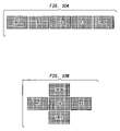
- FIGS. 10A and 10B depict various arrangements of five pixel arrays.
- FIG. 10A depicts five pixel arrays in a line having mirror color symmetry.
- FIG. 10B depicts five pixel arrays in a cross pattern having mirror color symmetry.
- FIGS. 11A-11D depict various techniques that may be used to address potential vignetting phenomenon problems associated with image sensors.
- FIG. 11A depicts an exemplary arrangement of a light circle and a pixel array that avoids the vignetting phenomenon.
- FIG. 11B depicts an exemplary arrangement of a plurality of light circles and a plurality of spaced-apart pixel arrays.
- FIG. 11C depicts in side view a plurality of spaced-apart pixel arrays relative to their light-circle generating lenses.
- FIG. 11D depicts in side view a plurality of pixel arrays separated by absorptive vertical walls instead of being spaced apart.
- FIG. 12 depicts an exemplary image sensor package of the invention.
- the invention pertains to an image sensor having a rear-illuminated architecture.
- a sensor includes an optically transparent substrate having first and second opposing surfaces, a detector layer in contact with the second surface, and a plurality of photodetectors.
- the first surface is a light-receiving surface, and the photodetectors are located in the detector layer.
- FIG. 2 A simple example of such a sensor architecture for a camera is shown in FIG. 2 .
- a microelectronic device 10 is provided comprising an optically transparent substrate 11 and a detector layer 20 .
- the substrate has parallel opposing front and rear surface, indicated at 12 and 14 , respectively.
- the front surface 12 is considered a light-receiving surface, and the detector layer 20 is positioned in contact with the rear surface 14 .
- a plurality of photodetectors 22 is provided in the detector layer 20 .
- no microlenses are provided.
- a camera lens 50 is placed over the array at a distance from the photodetectors 22 .
- light is transmitted through the camera lens 50 , the light-receiving surface 12 of the substrate, the interior of the substrate 11 , and the opposing surface 14 of the substrate, thereby impinging on the photodetectors 22 in the detector layer 20 .
- any of a number of materials may be used to form the transparent substrate.
- a number of ceramic materials are optically transparent.
- the term “ceramic” is generally used herein in its ordinary sense to indicate to a hard, brittle, heat-resistant and corrosion-resistant dielectric material made typically made by heating an inorganic compound, e.g., single or mixed metal oxides such as aluminum, zirconium or silicon oxides, nitrides, and carbides, at a high temperature.
- a ceramic material may be single crystalline, multicrystalline, or, as in the case of glass, amorphous.
- oxides have superior optical properties for use with the invention.
- exemplary oxides for use in the invention include silicon oxides (e.g., quartz or silicon-based glass) and aluminum oxides (e.g., sapphire). As discussed in detail below, these materials may be used with existing image-sensor processes, particularly those that involve the application of heat.
- the rear-illuminated architecture provides a number of advantages over the art. For example, when photodiodes are illuminated from the backside, there are no concerns with metal traces blocking the signal. In addition, the fill factor is larger. As discussed in detail below, increasing the fill factor decreases the need for microlenses and saves cost.
- the invention pertains to an image sensor that employs a plurality of photodetectors in a plurality of contiguous arrays.
- array is used herein in its ordinary sense and refers to a two-dimensional arrangement of features such as an arrangement of photodetectors, filters, or lenses. Arrays are generally comprised of regular, ordered features, as in, for example, a rectilinear grid, parallel stripes, spirals, and the like. An “array” differs from a “pattern” in that “patterns” do not necessarily contain regular and ordered features.
- the term “contiguous array” is to an array in which features are uninterrupted.
- contiguous array of a single first color generally should not contain any feature of another color between any two adjacent features of the first color.
- an array containing only red pixels uninterrupted by pixels of another color may be considered a contiguous array.
- a two-dimensional Bayer pattern of color pixels may be considered to include three coplanar arrays, i.e., a red pixel array, a green pixel array, and a blue pixel array, none of the three arrays may be considered “contiguous,” because the pixels of each color array is interrupted by interspersed pixels of the other two colors. Accordingly, two contiguous and coplanar arrays of features will not have any overlapping portions except, in certain instances, at their edges and/or corners.
- photodetector arrays are located in a detector layer.
- the arrays are coplanar to each other.
- the arrays may be located at increasing distances from a light-receiving surface of the image sensor.
- a sensor that incorporation this aspect of the invention typically, in contrast to those described in U.S. Pat. No. 6,632,701 to Merrill, include arrays located such that at least a portion of each array does not overlap another.
- the arrays may be substantially identical to or different from each other. For example, they may have the same or different number of photodetectors.
- the detector layer may be provided in the form of a chip, wafer, or a portion thereof.
- the detector layer may be constructed from any material that does not interfere with the operation of the photodetectors.
- photodetectors may take the form of photodiodes or photogates. The material may be selected according to the form of the photodetectors.
- the detector layer typically includes a semiconductor material.
- semiconductor is used herein in its ordinary sense to indicate any of various solid crystalline substances having electrical conductivity greater than insulators but less than good conductors.
- detector layers of the invention may include a single crystalline material consisting essentially of a single element, e.g., Si or Ge, or a compound semiconductor, e.g., a III-V semiconductor such as GaAs.
- the presence or absence of dopants is not critical to the invention, except when operability of the invention is in question.
- a multicrystalline or amorphous semiconductor material may be used.
- the invention may be advantageously employed in conjunction with technologies that employ either direct or indirect band gap semiconductors.
- silicon-based detector layers are often preferred regardless of the architecture of the image sensor.
- silicon-based detector layers may be advantageously used in both front-illuminated and rear-illuminated sensor architectures.
- certain optically transparent substrate materials are preferred when a silicon-based detector layer is used.
- rear illuminated sensors may be formed from silicon-on-insulator (SOI) wafers.
- SOI silicon-on-insulator
- Exemplary silicon-on-insulator systems include silicon-on-quartz (SOQ), silicon-on-glass (SOG) and silicon-on sapphire (SOS). It is expected that SOQ systems may be particularly suited for use with the invention because it permits standard high-temperature processing techniques involving, for example, thermal oxidation, diffusion, etc. As a result, substantial changes would not be required to existing image-sensor processes.
- one or more color filters may be positioned in a manner effective to allow selective transmission of light of particular wavelengths to each array.
- a plurality of lenses may be positioned in a manner effective to direct transmission of light to each array.
- an image sensor having first, second, and third photodetector arrays may employ: (a) one or more color filters positioned in a manner effective to allow selective transmission of light of first, second, and third wavelengths through the substrate to the first, second, and third arrays, respectively; and/or (b) first, second, and third lenses positioned in a manner effective to direct transmission of light to the first, second, and third arrays, respectively.
- known color image sensor architectures use one or more color filters over an array of photodetectors.
- the filters serve to block photos with wavelengths other than a wavelength (or range of wavelengths) of interest, allow the remaining photons to be collected by the underlying photodetectors.
- the color filter or filters are often arranged in a “Bayer pattern.” See, e.g., U.S. Pat. No. 3,971,065 to Bayer.
- An exemplary pixel array is having color filters arranged in a “Bayer pattern” is depicted in FIG. 3 .
- a four-by-four square array of green, red and blue filters provided that are of substantially identical size and shape. Each filter is located over a different photosensor. It should be apparent, then, that sixteen photosensors (not shown) are also arranged in a four-by-four array under the filters.
- Each row of the array contains filters of alternating colors. That is, each row contains alternating red and green filters or alternating green and blue filters. Similarly, each column contains filters of alternative colors. No two neighboring filters in a row or in a column share the same color. Green filters occupy half of all array sites, while red and blue filters each occupy a quarter of all array sites.
- certain known color image sensors require a plurality of microlenses. Typically, each photodetector requires its own microlens.
- the presence of microlenses do not eliminate the need for a larger imaging lens. Relative to the sensors that use the inventive sensor architecture, the use of color filters in a “Bayer pattern” and microlenses generally adds complexity and cost to images sensors.
- microlenses are also problematic for additional reasons.
- microlenses work for light coming in at close to normal incidence only. Light at the corners may be coming in at an angle to the sensor and be lost, resulting in darkness or vignetting (as discussed below).
- Microlenses also tend to be relatively soft and easily damaged. Thus, it is very hard to remove dust from the image sensor. By removing the microlenses from the sensor, the sensitivity and durability of the sensor is increased.
- microlenses are also implicated in causing purple fringe, an artifact common in digital imaging systems. It has been theorized that purple fringes are caused by chromatic aberration of the microlenses, particularly for light coming in off normal.
- some embodiments of the invention include an architecture that employs a plurality of contiguous pixel array.
- the sixteen pixels of FIG. 3 may be alternatively be arranged so that they form four substantially coplanar contiguous two-by-two arrays, as shown in FIG. 4 .
- the term “substantially” as used to describe the term “coplanar” as “in substantially coplanar” refers to the considerable degree to which items are in the same plane.
- the terms “substantial” and “substantially” are used analogously in other contexts involve an analogous definition.
- each array contains pixels of a single color.
- one red two-by-two array, one blue two-by-two array, and two green two-by-two arrays are formed. That is, instead of employing the Bayer pattern of color filters, each two-by-two array employs one or more filters of the same color. It should be apparent that the color filter arrangement shown in FIG. 4 is simpler and less expensive to produce than the color filter layout shown in FIG. 3 .
- array based image sensors for cameras generally require a camera lens for each photodetector array. As shown in FIG. 5 , the camera lens for each array should have a focal length equal to the lateral dimension of the photodetector array divided by the desired field of view angle. Otherwise, detectors may not be exposed to incoming light or incoming light will not impinge on a pixel.
- FIG. 6 depicts in side view the pixels arrays of FIGS. 3 and 4 , each array associated with its own camera lens.
- the pixels array of FIGS. 3 and 6A includes a single four-by-four matrix, while each pixel array of FIGS. 4 6 B includes four individual two-by-two matrix.
- the lateral dimension of the four-by-four pixel array is twice that of any one of the lateral dimension of the two-by-two pixel arrays.
- the focal length (F 4 ) of the lens for the four-by-four pixel array should be twice the focal length (F 2 ) of any of the lenses for each of the two-by-two pixel arrays. It follows, then, the image sensor architecture associated with a Bayer pattern sensor may require a height that is at least about twice needed for the image sensor architecture that includes a plurality of arrays.
- each array may employ a different lens positioned in a manner effective to direct transmission of light thereto.
- the associated lens may be required to handle a subset of the visible wavelength range. Accordingly, the chromatic requirements on the lens are relaxed.
- the lenses for each different color can be optimized to work best with that particular color. The relaxed wavelength requirements also reduce lens complexity and lead to lower cost.
- Lenses for use with the invention may be formed from any of materials that exhibit the appropriate optical properties for the intended application.
- the material must be transparent to optical radiation at wavelengths keyed to the sensitivity of the sensor.
- a lens may be formed from a ceramic material as described above and/or a polymeric material.
- the terms “polymer” or “polymeric” are used herein in their ordinary sense to refer to any of numerous natural and synthetic compounds of usually high molecular weight formed from a plurality of monomeric units, each typically having a low molecular weight. The terms include, for example, homopolymers as well copolymers, linear as well as branch and/or cyclic polymers, crosslinked as well as uncrosslinked polymers.
- Exemplary polymers suitable for use in the invention include those known in the microelectronic packaging industry such as those containing cyclic moieties, e.g., polycarbonates, polyimides, polyethylene terephthalates, and polystyrenes.
- polymer families such as polyarylene ethers, polyarylenes, and parylenes may be used as well.
- halogenated polymers may be used.
- Exemplary commercially available fluorinated and/or chlorinated polymers include polyvinylchloride, polyvinylfluoride, polyvinylidene fluoride, polyvinylidene chloride, polychorotrifluoroethylene, polytetrafluoroethylene, polyhexafluoropropylene, and copolymers thereof.
- the lenses may be formed individually or together. For example, three to five lenses could be implemented in one piece of injection molded polymer. Alternatively, the lenses could be written as a pattern in the interior of a single glass sheet otherwise.
- the lenses may also be made from etched glass. Both wet or dry etch techniques known in the art may be used to form the lenses of the invention. Similarly, techniques that use resist reflow or gray scale lithography may be used as well.
- Color filters when employed with the invention, may be provided in any of number of forms.
- color filters may be provided on-chip, e.g., as an integral part of a chip or wafer that contains detector layer.
- moving the color filters off-chip or off-wafer has advantages as well. For example, wafer cost may be reduced by moving color filters off-chip.
- off-chip manufacturing of bulk filter provides greater precision and performance from a manufacturing perspective.
- the color filters are not a requirement of the invention.
- the invention as an alternative to using color filters, takes advantage of the differential penetrative properties of photons of different wavelengths relative to the detector layer. For example, photons of different wavelengths penetrate silicon to different depths. Exploitation of this phenomenon has been described in U.S. Pat. No. 6,632,701 to Merrill.
- the present invention unlike the technologies described in the '701 patent, does not require different color sensors to be stacked on top of each other.
- all feature of an array may be located at a single depth.
- each array may be, for example, the different depth photodiodes could be arranged in a modified Bayer-Pattern as shown in FIG. 7 .
- FIG. 7 FIG.
- FIG. 7A depicts a typical Bayer pattern with color filters.
- FIG. 7B depicts an architecture similar to that of FIG. 7A except that it employs a modified Bayer pattern based on depth of penetration. As shown in FIG. 7B , the blue pixel has the shallowest junction depth and the all color pixel has the deepest.
- FIG. 8 depicts an image sensor that employs a prism-based to split incoming light into light to different wavelengths.
- the sensor includes a microelectronic device 10 is provided having parallel opposing front and rear surface, indicated at 12 and 14 , respectively.
- Three arrays of photodetectors 22 R, 22 G, 22 B are provided on in a detector layer 20 on the front surface 12 .
- Photodetectors 22 R are placed in a contiguous array that is positioned to receive red light from the set-up 60 .
- photodetectors 22 G and 22 B are placed in contiguous arrays positioned to receive green and blue light, respectively.
- Those of ordinary skill in the art will recognize that such light-splitting set-ups may include one or more mirrors, grating, filters, prisms, etc.
- FIG. 9 depicts how the various pixel arrays can be arranged in a number of different ways.
- three arrays may be arranged in a line with three different color filters or three different junction depths.
- four arrays may be employed as well.
- the fourth array may be used to detect all colors (with better low light performance, but saturation at higher light levels), all colors attenuated (to match the sensitivity of the other sensors).
- the fourth array may be used to detect green, so that the pixels of all arrays comport to the color proportionality of a Bayer pattern.
- FIG. 10 For the three or four array image sensors, some sections of an image may contain objects both close to and far from the camera lenses that include wavelengths covered by only one or two of the arrays.
- the information associated with the additional color wavelengths may have to be estimated in some way from adjacent pixels.
- FIG. 10A depicts a five pixel arrays arranged in a line.
- FIG. 10B shows five pixel arrays arranged in a cross.
- Blue light has the highest quantum efficiency in photodetectors such as photodiodes because it is of higher energy than either green or red light.
- color accuracy of blue light is typically the least important.
- the two red and green arrays serve to reduce the overall errors in magnitude versus having only single arrays for those colors.
- parallax When a plurality of contiguous arrays is employed, there may be some parallax associated with their lenses. This causes the images on each array to be slightly shifted relative to each other. It is possible to compensate for this shift during image processing by maximizing the cross correlation function between the arrays. This compensation can also correct for temperature effects due to potentially unequal thermal expansion of the image sensors and lenses.
- Another way to reduce parallax is through the arrangement of the arrays. For example, when four arrays are used, they may be arranged in a two-by-two matrix ( FIG. 9D ) rather than in a linear manner ( FIGS. 9B and 9C ). As another example, when three arrays are used, they may be arranged in a triangle pattern.
- Each object in the image can be shifted independently, depending on its distance from the camera.
- the amount of shift can be recorded to provide information on object distance, e.g., for three-dimensional imaging.
- the required shift and thus distance can also be fed into an auto-focus system. This system may operate dynamically to track objects in motion for more responsive focusing.
- One of ordinary skill in the art upon routine experimentation should be able to come up with mechanism, software, and other items to take advantage of the parallax phenomenon associated with the invention.
- Vignetting is another potential issue that should be addressed for image sensor technologies.
- vignetting occurs when an array of pixels receive attenuated light at its edges and/or corners relative to its center. This may occur when the array has an area greater than that of the light circle generated from focused incoming light.
- the light focused on a pixel array should extend beyond the pixel array, as shown in FIG. 11A .
- FIGS. 11B and 11C may be spaced apart to avoid cross talk from one lens' light circle overlapping another's photodetectors.
- the area between the pixel arrays can be used for readout electronics, etc.
- An alternative to spacing the arrays apart is to put absorptive vertical walls between the sensors as shown in FIG. 11D .
- the invention also provide images sensor packages that may employ any of the image sensors described above.
- the package may include a plurality of electrical contacts in electrical communication with the photodetectors.
- the contacts may be movable relative to the photodetectors, preferably in a sufficiently stress-relieving manner so as to maintain electrical communication with the photodetectors under repeated thermal cycling and other conditions.
- the packaging technology described in U.S. Pat. No. 6,465,893 to Khandros et al. may be used with the invention.
- FIG. 12 depicts an exemplary image sensor package of the invention that employs the packaging technologies described in the '893 patent.
- the image sensor of FIG. 12 employs a rear-illuminated architecture that includes a quartz substrate on a silicon detector layer. Photodetectors in the detector layer are in electrical communication with the bond pads. In turn, the bond pads are in electrical communication with contacts in the form of solder balls.
- Solder suitable for use with the invention may take any of a number of forms. Typically, balls or spheres are used. Pastes and other forms of solder may used as well. Regardless of the form of solder used, any various fusible alloys may be used. For example, eutectic solders containing tin and/or lead are known in the art. A flux may be advantageously used in conjunction with solder, since fluxless solder flow processes tend to be more costly. The flux may be present in the solder or in the passage.
- a solder resist typically an organic material, may be used to mask areas adjacent to the regions on which the solder may contact.
- the senor is placed on a compliant carrier, and the carrier is interposed between the sensor and the contacts in the form of solder balls.
- the compliant carrier allows the contacts to be movable relative to the photodetectors of the image sensor as well as other components of the image sensor.
- a camera module vendor does not have to buy and support the wire-bonding machines used for chip-on-board (COB) mounting of the image sensor die.
- COB chip-on-board
- a sensor may be attached to a printed wiring board in the same manner as other electronic component of a camera or a mobile device, e.g., by reflowing the sensor and other electronic components to a printed wiring board.
- the invention provides previously unknown advantages in the art of image sensor architecture leading to improved performances and/or reduction of cost.
- the invention does not require the use of a transparent cover and a cavity such as those described in U.S. Published Patent Application No. 2005/0095835 and may be adapted to maximize the aperture ratio for an image sensor.
- sensor performance is improved by increasing the signal-to-noise ratio and low-light sensitivity.
- efficiency and low-light sensitivity may be improved.
- the invention allows for the routing of conductive traces to be formed over instead of around pixels.
- the invention provides for a smaller and/or less costly chip than one made using a known architecture.
- the invention in some instances, allows sensors to use nearly 100% of incoming light without filter loss. No cavity or cover are required
- the invention enables a low cost, ultrahigh yield integrated package that may be less expensive to produce. Such a package is compatible with existing assembly infrastructure.
- the inventive image sensor may be constructed to contain or exclude specific feature according to the intended use of the sensor. That is, the inventive image sensor does not require the incorporation of all novel features of the invention.
- an optically transparent substrate may be used or omitted.
- antireflective and other optical coatings may be provided. The coating may serve more than one function.
- an alignment mechanism may be provided for aligning the components of the image sensors of the invention, e.g., the detectors, the filters, etc.
- aligning mechanisms or apparatuses known in the art e.g., mating features, clips, clamps, guides (mechanical, optical, electronic, or magnetic), devices used in metrology, etc.
- a locking mechanism may be used as well. The locking mechanism may be the same as or different from the aligning mechanism. Additional variations of the invention may be discovered upon routine experimentation without departing from the spirit of the present invention.
Abstract
Description
LUMINANCE=0.299*RED+0.587*GREEN+0.114*BLUE
Claims (25)
Priority Applications (3)
| Application Number | Priority Date | Filing Date | Title |
|---|---|---|---|
| US11/317,207 US7566853B2 (en) | 2005-08-12 | 2005-12-23 | Image sensor employing a plurality of photodetector arrays and/or rear-illuminated architecture |
| PCT/US2006/030121 WO2007021553A2 (en) | 2005-08-12 | 2006-08-02 | Image sensor employing a plurality of photodetector arrays and/ or rear-illuminated architecture |
| TW095129469A TWI317555B (en) | 2005-08-12 | 2006-08-11 | Image sensor employing a plurality of photodetector arrays and/or rear-illuminated architecture |
Applications Claiming Priority (2)
| Application Number | Priority Date | Filing Date | Title |
|---|---|---|---|
| US70781305P | 2005-08-12 | 2005-08-12 | |
| US11/317,207 US7566853B2 (en) | 2005-08-12 | 2005-12-23 | Image sensor employing a plurality of photodetector arrays and/or rear-illuminated architecture |
Publications (2)
| Publication Number | Publication Date |
|---|---|
| US20070034777A1 US20070034777A1 (en) | 2007-02-15 |
| US7566853B2 true US7566853B2 (en) | 2009-07-28 |
Family
ID=37387244
Family Applications (1)
| Application Number | Title | Priority Date | Filing Date |
|---|---|---|---|
| US11/317,207 Active 2027-05-23 US7566853B2 (en) | 2005-08-12 | 2005-12-23 | Image sensor employing a plurality of photodetector arrays and/or rear-illuminated architecture |
Country Status (3)
| Country | Link |
|---|---|
| US (1) | US7566853B2 (en) |
| TW (1) | TWI317555B (en) |
| WO (1) | WO2007021553A2 (en) |
Cited By (23)
| Publication number | Priority date | Publication date | Assignee | Title |
|---|---|---|---|---|
| US20110096032A1 (en) * | 2009-10-26 | 2011-04-28 | Seiko Epson Corporation | Optical position detecting device and display device with position detecting function |
| US20110096031A1 (en) * | 2009-10-26 | 2011-04-28 | Seiko Epson Corporation | Position detecting function-added projection display apparatus |
| US20130056844A1 (en) * | 2011-09-02 | 2013-03-07 | Vage Oganesian | Stepped Package For Image Sensor And Method Of Making Same |
| WO2014033099A2 (en) | 2012-08-27 | 2014-03-06 | Digital Optics Corporation Europe Limited | Rearview imaging systems for vehicle |
| US8714749B2 (en) | 2009-11-06 | 2014-05-06 | Seiko Epson Corporation | Projection display device with position detection function |
| WO2014072837A2 (en) | 2012-06-07 | 2014-05-15 | DigitalOptics Corporation Europe Limited | Mems fast focus camera module |
| US9001268B2 (en) | 2012-08-10 | 2015-04-07 | Nan Chang O-Film Optoelectronics Technology Ltd | Auto-focus camera module with flexible printed circuit extension |
| US9007520B2 (en) | 2012-08-10 | 2015-04-14 | Nanchang O-Film Optoelectronics Technology Ltd | Camera module with EMI shield |
| US9091843B1 (en) | 2014-03-16 | 2015-07-28 | Hyperion Development, LLC | Optical assembly for a wide field of view point action camera with low track length to focal length ratio |
| US9316808B1 (en) | 2014-03-16 | 2016-04-19 | Hyperion Development, LLC | Optical assembly for a wide field of view point action camera with a low sag aspheric lens element |
| US9316820B1 (en) | 2014-03-16 | 2016-04-19 | Hyperion Development, LLC | Optical assembly for a wide field of view point action camera with low astigmatism |
| US9496247B2 (en) | 2013-08-26 | 2016-11-15 | Optiz, Inc. | Integrated camera module and method of making same |
| US9494772B1 (en) | 2014-03-16 | 2016-11-15 | Hyperion Development, LLC | Optical assembly for a wide field of view point action camera with low field curvature |
| US9525807B2 (en) | 2010-12-01 | 2016-12-20 | Nan Chang O-Film Optoelectronics Technology Ltd | Three-pole tilt control system for camera module |
| US9726859B1 (en) | 2014-03-16 | 2017-08-08 | Navitar Industries, Llc | Optical assembly for a wide field of view camera with low TV distortion |
| US9995910B1 (en) | 2014-03-16 | 2018-06-12 | Navitar Industries, Llc | Optical assembly for a compact wide field of view digital camera with high MTF |
| WO2018140697A1 (en) | 2017-01-26 | 2018-08-02 | Navitar, Inc. | High etendue modular zoom lens for machine vision |
| US10101636B2 (en) | 2012-12-31 | 2018-10-16 | Digitaloptics Corporation | Auto-focus camera module with MEMS capacitance estimator |
| US10138539B1 (en) * | 2018-04-03 | 2018-11-27 | Shiping Cheng | Method of managing coating uniformity with an optical thickness monitoring system |
| US10139595B1 (en) | 2014-03-16 | 2018-11-27 | Navitar Industries, Llc | Optical assembly for a compact wide field of view digital camera with low first lens diameter to image diagonal ratio |
| US10386604B1 (en) | 2014-03-16 | 2019-08-20 | Navitar Industries, Llc | Compact wide field of view digital camera with stray light impact suppression |
| US10545314B1 (en) | 2014-03-16 | 2020-01-28 | Navitar Industries, Llc | Optical assembly for a compact wide field of view digital camera with low lateral chromatic aberration |
| US10847564B1 (en) | 2019-07-24 | 2020-11-24 | Taiwan Semiconductor Manufacturing Co., Ltd. | Charge release layer to remove charge carriers from dielectric grid structures in image sensors |
Families Citing this family (24)
| Publication number | Priority date | Publication date | Assignee | Title |
|---|---|---|---|---|
| KR100674711B1 (en) * | 2005-12-28 | 2007-01-25 | 삼성전기주식회사 | Optical lens system of a mobile camera |
| JP2007235418A (en) * | 2006-02-28 | 2007-09-13 | Toshiba Corp | Solid state image pickup device |
| US7924483B2 (en) * | 2006-03-06 | 2011-04-12 | Smith Scott T | Fused multi-array color image sensor |
| US8247801B2 (en) * | 2006-03-31 | 2012-08-21 | Imec | Organic semi-conductor photo-detecting device |
| US8053853B2 (en) | 2006-05-03 | 2011-11-08 | Taiwan Semiconductor Manufacturing Company, Ltd. | Color filter-embedded MSM image sensor |
| KR100871564B1 (en) * | 2006-06-19 | 2008-12-02 | 삼성전기주식회사 | Camera module |
| KR100772910B1 (en) * | 2006-06-26 | 2007-11-05 | 삼성전기주식회사 | Digital camera module |
| EP1874034A3 (en) * | 2006-06-26 | 2011-12-21 | Samsung Electro-Mechanics Co., Ltd. | Apparatus and method of recovering high pixel image |
| US8054371B2 (en) * | 2007-02-19 | 2011-11-08 | Taiwan Semiconductor Manufacturing Company, Ltd. | Color filter for image sensor |
| US7738017B2 (en) * | 2007-03-27 | 2010-06-15 | Aptina Imaging Corporation | Method and apparatus for automatic linear shift parallax correction for multi-array image systems |
| TWI347000B (en) * | 2007-06-11 | 2011-08-11 | Xintec Inc | Integrated circuit package and operation, fabrication method thereof |
| US20090201400A1 (en) * | 2008-02-08 | 2009-08-13 | Omnivision Technologies, Inc. | Backside illuminated image sensor with global shutter and storage capacitor |
| FR2941327B1 (en) * | 2009-01-22 | 2012-05-04 | St Microelectronics Sa | IMAGE ENTRY DEVICE COMPRISING MEANS FOR PIXEL COLLECTING. |
| DE102009013112A1 (en) | 2009-03-13 | 2010-09-16 | Fraunhofer-Gesellschaft zur Förderung der angewandten Forschung e.V. | Method for producing a multiplicity of microoptoelectronic components and microoptoelectronic component |
| JP5421364B2 (en) * | 2010-01-05 | 2014-02-19 | パナソニック株式会社 | 3D imaging device |
| US9137503B2 (en) | 2010-11-03 | 2015-09-15 | Sony Corporation | Lens and color filter arrangement, super-resolution camera system and method |
| EP2461198A3 (en) | 2010-12-01 | 2017-03-08 | BlackBerry Limited | Apparatus, and associated method, for a camera module of electronic device |
| EP2592837A1 (en) * | 2011-11-10 | 2013-05-15 | Research In Motion Limited | Apparatus and associated method for forming color camera image |
| US8906320B1 (en) | 2012-04-16 | 2014-12-09 | Illumina, Inc. | Biosensors for biological or chemical analysis and systems and methods for same |
| CN103973856B (en) * | 2013-02-05 | 2016-12-28 | 联想移动通信科技有限公司 | A kind of mobile terminal |
| US10605734B2 (en) * | 2013-04-03 | 2020-03-31 | Life Technologies Corporation | Systems and methods for genetic sequencing |
| US9881966B2 (en) * | 2015-07-17 | 2018-01-30 | International Business Machines Corporation | Three-dimensional integrated multispectral imaging sensor |
| EP3419053A1 (en) | 2017-06-21 | 2018-12-26 | Life Technologies GmbH | Optical component with waveguide based filter |
| MX2019015838A (en) * | 2017-12-26 | 2020-08-03 | Illumina Inc | Sensor system. |
Citations (87)
| Publication number | Priority date | Publication date | Assignee | Title |
|---|---|---|---|---|
| US2507956A (en) | 1947-11-01 | 1950-05-16 | Lithographic Technical Foundat | Process of coating aluminum |
| US2796370A (en) | 1955-03-04 | 1957-06-18 | Charles W Ostrander | Composition and method for producing corrosion resistant protective coating on aluminum and aluminum alloys |
| US2851385A (en) | 1952-04-03 | 1958-09-09 | Amchem Prod | Process and composition for coating aluminum surfaces |
| US3971065A (en) | 1975-03-05 | 1976-07-20 | Eastman Kodak Company | Color imaging array |
| US3981023A (en) | 1974-09-16 | 1976-09-14 | Northern Electric Company Limited | Integral lens light emitting diode |
| US4027323A (en) | 1976-09-07 | 1977-05-31 | Honeywell Inc. | Photodetector array delineation method |
| US4069095A (en) | 1976-09-07 | 1978-01-17 | Honeywell Inc. | Method of preparing photodetector array elements |
| US4196508A (en) | 1977-09-01 | 1980-04-08 | Honeywell Inc. | Durable insulating protective layer for hybrid CCD/mosaic IR detector array |
| US4197633A (en) | 1977-09-01 | 1980-04-15 | Honeywell, Inc. | Hybrid mosaic IR/CCD focal plane |
| US4259679A (en) | 1977-01-17 | 1981-03-31 | Plessey Handel Und Investments A.G. | Display devices |
| US4275407A (en) | 1977-09-01 | 1981-06-23 | Honeywell Inc. | Durable insulating protective layer for hybrid CCD/mosaic IR detector array |
| US4279690A (en) | 1975-10-28 | 1981-07-21 | Texas Instruments Incorporated | High-radiance emitters with integral microlens |
| US4339689A (en) | 1979-01-29 | 1982-07-13 | Matsushita Electric Industrial Co., Ltd. | Light emitting diode and method of making the same |
| US4351101A (en) | 1980-10-20 | 1982-09-28 | Honeywell Inc. | Semiconductor device processing for readily and reliably forming electrical interconnects to contact pads |
| WO1985002283A1 (en) | 1983-11-07 | 1985-05-23 | Irvine Sensors Corporation | Detector array module-structure and fabrication |
| US4551629A (en) | 1980-09-16 | 1985-11-05 | Irvine Sensors Corporation | Detector array module-structure and fabrication |
| JPS63166710A (en) | 1986-12-22 | 1988-07-09 | ダウ・コーニング・コーポレーシヨン | Manufacture of silicon by reducing silicon dioxide with solid carbonaceous reducing agent |
| US4764846A (en) | 1987-01-05 | 1988-08-16 | Irvine Sensors Corporation | High density electronic package comprising stacked sub-modules |
| US4794092A (en) | 1987-11-18 | 1988-12-27 | Grumman Aerospace Corporation | Single wafer moated process |
| US4797179A (en) | 1987-06-09 | 1989-01-10 | Lytel Corporation | Fabrication of integral lenses on LED devices |
| WO1989004113A1 (en) | 1987-10-20 | 1989-05-05 | Irvine Sensors Corporation | High-density electronic modules, process and product |
| US4862249A (en) | 1987-04-17 | 1989-08-29 | Xoc Devices, Inc. | Packaging system for stacking integrated circuits |
| US4933601A (en) | 1987-12-09 | 1990-06-12 | Hitachi Cable Limited | Light emitting diode array chip and method of fabricating same |
| US4984358A (en) | 1989-03-10 | 1991-01-15 | Microelectronics And Computer Technology Corporation | Method of assembling stacks of integrated circuit dies |
| US5037779A (en) | 1989-05-19 | 1991-08-06 | Whalley Peter D | Method of encapsulating a sensor device using capillary action and the device so encapsulated |
| US5081520A (en) | 1989-05-16 | 1992-01-14 | Minolta Camera Kabushiki Kaisha | Chip mounting substrate having an integral molded projection and conductive pattern |
| US5104820A (en) | 1989-07-07 | 1992-04-14 | Irvine Sensors Corporation | Method of fabricating electronic circuitry unit containing stacked IC layers having lead rerouting |
| US5118924A (en) | 1990-10-01 | 1992-06-02 | Eastman Kodak Company | Static control overlayers on opto-electronic devices |
| EP0490739A1 (en) | 1990-12-11 | 1992-06-17 | Thomson-Csf | Interconnection method and device for three-dimensional integrated circuits |
| US5124543A (en) | 1989-08-09 | 1992-06-23 | Ricoh Company, Ltd. | Light emitting element, image sensor and light receiving element with linearly varying waveguide index |
| US5126286A (en) | 1990-10-05 | 1992-06-30 | Micron Technology, Inc. | Method of manufacturing edge connected semiconductor die |
| US5177753A (en) | 1990-06-14 | 1993-01-05 | Rohm Co., Ltd. | Semi-conductor laser unit |
| US5250462A (en) | 1990-08-24 | 1993-10-05 | Nec Corporation | Method for fabricating an optical semiconductor device |
| US5266501A (en) | 1991-05-09 | 1993-11-30 | Kabushiki Kaisha Toshiba | Method for manufacturing a solid state image sensing device using transparent thermosetting resin layers |
| US5266833A (en) | 1992-03-30 | 1993-11-30 | Capps David F | Integrated circuit bus structure |
| US5321303A (en) | 1985-12-20 | 1994-06-14 | Seiko Instruments Inc. | Semiconductor device having linearly arranged semiconductor chips |
| US5342681A (en) | 1992-08-28 | 1994-08-30 | Texas Instruments Incorporated | Absorbing, low reflecting coating for visible and infrared light |
| EP0650199A1 (en) | 1993-10-22 | 1995-04-26 | Canon Kabushiki Kaisha | Filter for image sensor |
| US5455455A (en) | 1992-09-14 | 1995-10-03 | Badehi; Peirre | Methods for producing packaged integrated circuit devices and packaged integrated circuit devices produced thereby |
| US5455386A (en) | 1994-01-14 | 1995-10-03 | Olin Corporation | Chamfered electronic package component |
| US5500540A (en) | 1994-04-15 | 1996-03-19 | Photonics Research Incorporated | Wafer scale optoelectronic package |
| US5526449A (en) | 1993-01-08 | 1996-06-11 | Massachusetts Institute Of Technology | Optoelectronic integrated circuits and method of fabricating and reducing losses using same |
| US5546654A (en) | 1994-08-29 | 1996-08-20 | General Electric Company | Vacuum fixture and method for fabricating electronic assemblies |
| US5567657A (en) | 1995-12-04 | 1996-10-22 | General Electric Company | Fabrication and structures of two-sided molded circuit modules with flexible interconnect layers |
| US5595930A (en) | 1995-06-22 | 1997-01-21 | Lg Semicon Co., Ltd. | Method of manufacturing CCD image sensor by use of recesses |
| US5612570A (en) | 1995-04-13 | 1997-03-18 | Dense-Pac Microsystems, Inc. | Chip stack and method of making same |
| US5657206A (en) | 1994-06-23 | 1997-08-12 | Cubic Memory, Inc. | Conductive epoxy flip-chip package and method |
| EP0790653A2 (en) | 1995-09-01 | 1997-08-20 | Canon Kabushiki Kaisha | IC package and its assembly method |
| US5661087A (en) | 1994-06-23 | 1997-08-26 | Cubic Memory, Inc. | Vertical interconnect process for silicon segments |
| US5672519A (en) | 1994-02-23 | 1997-09-30 | Lg Semicon Co., Ltd. | Method of fabricating solid state image sensing elements |
| US5677200A (en) | 1995-05-12 | 1997-10-14 | Lg Semicond Co., Ltd. | Color charge-coupled device and method of manufacturing the same |
| EP0810659A2 (en) | 1996-05-28 | 1997-12-03 | Harris Corporation | Semiconductor packaging apparatus and method |
| US5716759A (en) | 1993-09-02 | 1998-02-10 | Shellcase Ltd. | Method and apparatus for producing integrated circuit devices |
| US5814894A (en) | 1995-04-07 | 1998-09-29 | Nitto Denko Corporation | Semiconductor device, production method thereof, and tape carrier for semiconductor device used for producing the semiconductor device |
| US5817541A (en) | 1997-03-20 | 1998-10-06 | Raytheon Company | Methods of fabricating an HDMI decal chip scale package |
| US5837562A (en) | 1995-07-07 | 1998-11-17 | The Charles Stark Draper Laboratory, Inc. | Process for bonding a shell to a substrate for packaging a semiconductor |
| US5849623A (en) | 1994-12-05 | 1998-12-15 | General Electric Company | Method of forming thin film resistors on organic surfaces |
| US5857858A (en) | 1996-12-23 | 1999-01-12 | General Electric Company | Demountable and repairable low pitch interconnect for stacked multichip modules |
| US5859475A (en) | 1996-04-24 | 1999-01-12 | Amkor Technology, Inc. | Carrier strip and molded flex circuit ball grid array |
| US5869353A (en) | 1997-11-17 | 1999-02-09 | Dense-Pac Microsystems, Inc. | Modular panel stacking process |
| US5888884A (en) | 1998-01-02 | 1999-03-30 | General Electric Company | Electronic device pad relocation, precision placement, and packaging in arrays |
| US5891761A (en) | 1994-06-23 | 1999-04-06 | Cubic Memory, Inc. | Method for forming vertical interconnect process for silicon segments with thermally conductive epoxy preform |
| US5900674A (en) | 1996-12-23 | 1999-05-04 | General Electric Company | Interface structures for electronic devices |
| US5909052A (en) | 1986-03-12 | 1999-06-01 | Hitachi, Ltd. | Semiconductor device having plural chips with the sides of the chips in face-to-face contact with each other in the same crystal plane |
| US5938452A (en) | 1996-12-23 | 1999-08-17 | General Electric Company | Flexible interface structures for electronic devices |
| US5952712A (en) | 1996-07-18 | 1999-09-14 | Nec Corporation | Packaged semiconductor device and method of manufacturing the same |
| US5986746A (en) | 1994-02-18 | 1999-11-16 | Imedge Technology Inc. | Topographical object detection system |
| JPH11326366A (en) | 1998-05-13 | 1999-11-26 | Murata Mfg Co Ltd | Semiconductor electronic component device and its manufacture |
| US5993981A (en) | 1997-04-18 | 1999-11-30 | Raytheon Company | Broadband protective optical window coating |
| US6020217A (en) | 1997-02-21 | 2000-02-01 | Daimler-Benz Aktiengesellschaft | Semiconductor devices with CSP packages and method for making them |
| US6022758A (en) | 1994-07-10 | 2000-02-08 | Shellcase Ltd. | Process for manufacturing solder leads on a semiconductor device package |
| US6040235A (en) | 1994-01-17 | 2000-03-21 | Shellcase Ltd. | Methods and apparatus for producing integrated circuit devices |
| US6072236A (en) | 1996-03-07 | 2000-06-06 | Micron Technology, Inc. | Micromachined chip scale package |
| US6080596A (en) | 1994-06-23 | 2000-06-27 | Cubic Memory Inc. | Method for forming vertical interconnect process for silicon segments with dielectric isolation |
| US6083766A (en) | 1999-07-01 | 2000-07-04 | Viking Tech Corporation | Packaging method of thin film passive components on silicon chip |
| US6087586A (en) | 1997-05-13 | 2000-07-11 | Caesar Technology, Inc. | Chip scale package |
| US6106735A (en) | 1997-01-11 | 2000-08-22 | Robert Bosch Gmbh | Wafer stack and method of producing sensors |
| US6235141B1 (en) | 1996-09-27 | 2001-05-22 | Digital Optics Corporation | Method of mass producing and packaging integrated optical subsystems |
| US6307261B1 (en) | 1992-05-27 | 2001-10-23 | Thomson Csf | Method for the manufacturing of a semiconductor device which comprises at least one chip and corresponding device |
| US6329708B1 (en) | 1999-04-26 | 2001-12-11 | Oki Electric Industry Co. Ltd. | Micro ball grid array semiconductor device and semiconductor module |
| US6590291B2 (en) | 2000-01-31 | 2003-07-08 | Shinko Electric Industries Co., Ltd. | Semiconductor device and manufacturing method therefor |
| US6646289B1 (en) | 1998-02-06 | 2003-11-11 | Shellcase Ltd. | Integrated circuit device |
| US20050074954A1 (en) | 2002-10-11 | 2005-04-07 | Hideo Yamanaka | Method and apparatus for producing ultra-thin semiconductor chip and method and apparatus for producing ultra-thin back-illuminated solid-state image pickup device |
| US6891256B2 (en) | 2001-10-22 | 2005-05-10 | Fairchild Semiconductor Corporation | Thin, thermally enhanced flip chip in a leaded molded package |
| US6977431B1 (en) | 2003-11-05 | 2005-12-20 | Amkor Technology, Inc. | Stackable semiconductor package and manufacturing method thereof |
| US7033664B2 (en) | 2002-10-22 | 2006-04-25 | Tessera Technologies Hungary Kft | Methods for producing packaged integrated circuit devices and packaged integrated circuit devices produced thereby |
| US7425460B2 (en) * | 2004-09-17 | 2008-09-16 | California Institute Of Technology | Method for implementation of back-illuminated CMOS or CCD imagers |
-
2005
- 2005-12-23 US US11/317,207 patent/US7566853B2/en active Active
-
2006
- 2006-08-02 WO PCT/US2006/030121 patent/WO2007021553A2/en active Application Filing
- 2006-08-11 TW TW095129469A patent/TWI317555B/en active
Patent Citations (100)
| Publication number | Priority date | Publication date | Assignee | Title |
|---|---|---|---|---|
| US2507956A (en) | 1947-11-01 | 1950-05-16 | Lithographic Technical Foundat | Process of coating aluminum |
| US2851385A (en) | 1952-04-03 | 1958-09-09 | Amchem Prod | Process and composition for coating aluminum surfaces |
| US2796370A (en) | 1955-03-04 | 1957-06-18 | Charles W Ostrander | Composition and method for producing corrosion resistant protective coating on aluminum and aluminum alloys |
| US3981023A (en) | 1974-09-16 | 1976-09-14 | Northern Electric Company Limited | Integral lens light emitting diode |
| US3971065A (en) | 1975-03-05 | 1976-07-20 | Eastman Kodak Company | Color imaging array |
| US4279690A (en) | 1975-10-28 | 1981-07-21 | Texas Instruments Incorporated | High-radiance emitters with integral microlens |
| US4027323A (en) | 1976-09-07 | 1977-05-31 | Honeywell Inc. | Photodetector array delineation method |
| US4069095A (en) | 1976-09-07 | 1978-01-17 | Honeywell Inc. | Method of preparing photodetector array elements |
| US4259679A (en) | 1977-01-17 | 1981-03-31 | Plessey Handel Und Investments A.G. | Display devices |
| US4196508A (en) | 1977-09-01 | 1980-04-08 | Honeywell Inc. | Durable insulating protective layer for hybrid CCD/mosaic IR detector array |
| US4197633A (en) | 1977-09-01 | 1980-04-15 | Honeywell, Inc. | Hybrid mosaic IR/CCD focal plane |
| US4275407A (en) | 1977-09-01 | 1981-06-23 | Honeywell Inc. | Durable insulating protective layer for hybrid CCD/mosaic IR detector array |
| US4339689A (en) | 1979-01-29 | 1982-07-13 | Matsushita Electric Industrial Co., Ltd. | Light emitting diode and method of making the same |
| US4551629A (en) | 1980-09-16 | 1985-11-05 | Irvine Sensors Corporation | Detector array module-structure and fabrication |
| US4351101A (en) | 1980-10-20 | 1982-09-28 | Honeywell Inc. | Semiconductor device processing for readily and reliably forming electrical interconnects to contact pads |
| WO1985002283A1 (en) | 1983-11-07 | 1985-05-23 | Irvine Sensors Corporation | Detector array module-structure and fabrication |
| US5321303A (en) | 1985-12-20 | 1994-06-14 | Seiko Instruments Inc. | Semiconductor device having linearly arranged semiconductor chips |
| US5909052A (en) | 1986-03-12 | 1999-06-01 | Hitachi, Ltd. | Semiconductor device having plural chips with the sides of the chips in face-to-face contact with each other in the same crystal plane |
| JPS63166710A (en) | 1986-12-22 | 1988-07-09 | ダウ・コーニング・コーポレーシヨン | Manufacture of silicon by reducing silicon dioxide with solid carbonaceous reducing agent |
| US4764846A (en) | 1987-01-05 | 1988-08-16 | Irvine Sensors Corporation | High density electronic package comprising stacked sub-modules |
| US4862249A (en) | 1987-04-17 | 1989-08-29 | Xoc Devices, Inc. | Packaging system for stacking integrated circuits |
| US4797179A (en) | 1987-06-09 | 1989-01-10 | Lytel Corporation | Fabrication of integral lenses on LED devices |
| WO1989004113A1 (en) | 1987-10-20 | 1989-05-05 | Irvine Sensors Corporation | High-density electronic modules, process and product |
| US4794092A (en) | 1987-11-18 | 1988-12-27 | Grumman Aerospace Corporation | Single wafer moated process |
| US4933601A (en) | 1987-12-09 | 1990-06-12 | Hitachi Cable Limited | Light emitting diode array chip and method of fabricating same |
| US4984358A (en) | 1989-03-10 | 1991-01-15 | Microelectronics And Computer Technology Corporation | Method of assembling stacks of integrated circuit dies |
| US5081520A (en) | 1989-05-16 | 1992-01-14 | Minolta Camera Kabushiki Kaisha | Chip mounting substrate having an integral molded projection and conductive pattern |
| US5037779A (en) | 1989-05-19 | 1991-08-06 | Whalley Peter D | Method of encapsulating a sensor device using capillary action and the device so encapsulated |
| US5104820A (en) | 1989-07-07 | 1992-04-14 | Irvine Sensors Corporation | Method of fabricating electronic circuitry unit containing stacked IC layers having lead rerouting |
| US5124543A (en) | 1989-08-09 | 1992-06-23 | Ricoh Company, Ltd. | Light emitting element, image sensor and light receiving element with linearly varying waveguide index |
| US5177753A (en) | 1990-06-14 | 1993-01-05 | Rohm Co., Ltd. | Semi-conductor laser unit |
| US5250462A (en) | 1990-08-24 | 1993-10-05 | Nec Corporation | Method for fabricating an optical semiconductor device |
| US5118924A (en) | 1990-10-01 | 1992-06-02 | Eastman Kodak Company | Static control overlayers on opto-electronic devices |
| US5126286A (en) | 1990-10-05 | 1992-06-30 | Micron Technology, Inc. | Method of manufacturing edge connected semiconductor die |
| EP0490739A1 (en) | 1990-12-11 | 1992-06-17 | Thomson-Csf | Interconnection method and device for three-dimensional integrated circuits |
| US5266501A (en) | 1991-05-09 | 1993-11-30 | Kabushiki Kaisha Toshiba | Method for manufacturing a solid state image sensing device using transparent thermosetting resin layers |
| US5266833A (en) | 1992-03-30 | 1993-11-30 | Capps David F | Integrated circuit bus structure |
| US6307261B1 (en) | 1992-05-27 | 2001-10-23 | Thomson Csf | Method for the manufacturing of a semiconductor device which comprises at least one chip and corresponding device |
| US5393574A (en) | 1992-08-28 | 1995-02-28 | Texas Instruments Incorporated | Method for forming light absorbing aluminum nitride films by ion beam deposition |
| US5342681A (en) | 1992-08-28 | 1994-08-30 | Texas Instruments Incorporated | Absorbing, low reflecting coating for visible and infrared light |
| US5455455A (en) | 1992-09-14 | 1995-10-03 | Badehi; Peirre | Methods for producing packaged integrated circuit devices and packaged integrated circuit devices produced thereby |
| US5547906A (en) | 1992-09-14 | 1996-08-20 | Badehi; Pierre | Methods for producing integrated circuit devices |
| US5526449A (en) | 1993-01-08 | 1996-06-11 | Massachusetts Institute Of Technology | Optoelectronic integrated circuits and method of fabricating and reducing losses using same |
| US5716759A (en) | 1993-09-02 | 1998-02-10 | Shellcase Ltd. | Method and apparatus for producing integrated circuit devices |
| EP0650199A1 (en) | 1993-10-22 | 1995-04-26 | Canon Kabushiki Kaisha | Filter for image sensor |
| US5455386A (en) | 1994-01-14 | 1995-10-03 | Olin Corporation | Chamfered electronic package component |
| US6040235A (en) | 1994-01-17 | 2000-03-21 | Shellcase Ltd. | Methods and apparatus for producing integrated circuit devices |
| US5986746A (en) | 1994-02-18 | 1999-11-16 | Imedge Technology Inc. | Topographical object detection system |
| US5672519A (en) | 1994-02-23 | 1997-09-30 | Lg Semicon Co., Ltd. | Method of fabricating solid state image sensing elements |
| US5500540A (en) | 1994-04-15 | 1996-03-19 | Photonics Research Incorporated | Wafer scale optoelectronic package |
| US5661087A (en) | 1994-06-23 | 1997-08-26 | Cubic Memory, Inc. | Vertical interconnect process for silicon segments |
| US5675180A (en) | 1994-06-23 | 1997-10-07 | Cubic Memory, Inc. | Vertical interconnect process for silicon segments |
| US6098278A (en) | 1994-06-23 | 2000-08-08 | Cubic Memory, Inc. | Method for forming conductive epoxy flip-chip on chip |
| US5891761A (en) | 1994-06-23 | 1999-04-06 | Cubic Memory, Inc. | Method for forming vertical interconnect process for silicon segments with thermally conductive epoxy preform |
| US5657206A (en) | 1994-06-23 | 1997-08-12 | Cubic Memory, Inc. | Conductive epoxy flip-chip package and method |
| US6080596A (en) | 1994-06-23 | 2000-06-27 | Cubic Memory Inc. | Method for forming vertical interconnect process for silicon segments with dielectric isolation |
| US5837566A (en) | 1994-06-23 | 1998-11-17 | Cubic Memory, Inc. | Vertical interconnect process for silicon segments |
| US6022758A (en) | 1994-07-10 | 2000-02-08 | Shellcase Ltd. | Process for manufacturing solder leads on a semiconductor device package |
| US5546654A (en) | 1994-08-29 | 1996-08-20 | General Electric Company | Vacuum fixture and method for fabricating electronic assemblies |
| US5849623A (en) | 1994-12-05 | 1998-12-15 | General Electric Company | Method of forming thin film resistors on organic surfaces |
| US6134118A (en) | 1995-01-19 | 2000-10-17 | Cubic Memory Inc. | Conductive epoxy flip-chip package and method |
| US5814894A (en) | 1995-04-07 | 1998-09-29 | Nitto Denko Corporation | Semiconductor device, production method thereof, and tape carrier for semiconductor device used for producing the semiconductor device |
| US5612570A (en) | 1995-04-13 | 1997-03-18 | Dense-Pac Microsystems, Inc. | Chip stack and method of making same |
| US5677200A (en) | 1995-05-12 | 1997-10-14 | Lg Semicond Co., Ltd. | Color charge-coupled device and method of manufacturing the same |
| US5595930A (en) | 1995-06-22 | 1997-01-21 | Lg Semicon Co., Ltd. | Method of manufacturing CCD image sensor by use of recesses |
| US5837562A (en) | 1995-07-07 | 1998-11-17 | The Charles Stark Draper Laboratory, Inc. | Process for bonding a shell to a substrate for packaging a semiconductor |
| EP0790653A2 (en) | 1995-09-01 | 1997-08-20 | Canon Kabushiki Kaisha | IC package and its assembly method |
| US5567657A (en) | 1995-12-04 | 1996-10-22 | General Electric Company | Fabrication and structures of two-sided molded circuit modules with flexible interconnect layers |
| US5703400A (en) | 1995-12-04 | 1997-12-30 | General Electric Company | Fabrication and structures of two-sided molded circuit modules with flexible interconnect layers |
| US6072236A (en) | 1996-03-07 | 2000-06-06 | Micron Technology, Inc. | Micromachined chip scale package |
| US5859475A (en) | 1996-04-24 | 1999-01-12 | Amkor Technology, Inc. | Carrier strip and molded flex circuit ball grid array |
| US6124637A (en) | 1996-04-24 | 2000-09-26 | Amkor Technology, Inc. | Carrier strip and molded flex circuit ball grid array and method of making |
| US5985695A (en) | 1996-04-24 | 1999-11-16 | Amkor Technology, Inc. | Method of making a molded flex circuit ball grid array |
| US5965933A (en) | 1996-05-28 | 1999-10-12 | Young; William R. | Semiconductor packaging apparatus |
| EP0810659A2 (en) | 1996-05-28 | 1997-12-03 | Harris Corporation | Semiconductor packaging apparatus and method |
| US5952712A (en) | 1996-07-18 | 1999-09-14 | Nec Corporation | Packaged semiconductor device and method of manufacturing the same |
| US6235141B1 (en) | 1996-09-27 | 2001-05-22 | Digital Optics Corporation | Method of mass producing and packaging integrated optical subsystems |
| US5938452A (en) | 1996-12-23 | 1999-08-17 | General Electric Company | Flexible interface structures for electronic devices |
| US6092280A (en) | 1996-12-23 | 2000-07-25 | General Electric Co. | Flexible interface structures for electronic devices |
| US5900674A (en) | 1996-12-23 | 1999-05-04 | General Electric Company | Interface structures for electronic devices |
| US6046410A (en) | 1996-12-23 | 2000-04-04 | General Electric Company | Interface structures for electronic devices |
| US5857858A (en) | 1996-12-23 | 1999-01-12 | General Electric Company | Demountable and repairable low pitch interconnect for stacked multichip modules |
| US6106735A (en) | 1997-01-11 | 2000-08-22 | Robert Bosch Gmbh | Wafer stack and method of producing sensors |
| US6020217A (en) | 1997-02-21 | 2000-02-01 | Daimler-Benz Aktiengesellschaft | Semiconductor devices with CSP packages and method for making them |
| US5817541A (en) | 1997-03-20 | 1998-10-06 | Raytheon Company | Methods of fabricating an HDMI decal chip scale package |
| US5993981A (en) | 1997-04-18 | 1999-11-30 | Raytheon Company | Broadband protective optical window coating |
| US6087586A (en) | 1997-05-13 | 2000-07-11 | Caesar Technology, Inc. | Chip scale package |
| US5869353A (en) | 1997-11-17 | 1999-02-09 | Dense-Pac Microsystems, Inc. | Modular panel stacking process |
| US6002163A (en) | 1998-01-02 | 1999-12-14 | General Electric Company | Electronic device pad relocation, precision placement, and packaging in arrays |
| US5888884A (en) | 1998-01-02 | 1999-03-30 | General Electric Company | Electronic device pad relocation, precision placement, and packaging in arrays |
| US6646289B1 (en) | 1998-02-06 | 2003-11-11 | Shellcase Ltd. | Integrated circuit device |
| JPH11326366A (en) | 1998-05-13 | 1999-11-26 | Murata Mfg Co Ltd | Semiconductor electronic component device and its manufacture |
| US6329708B1 (en) | 1999-04-26 | 2001-12-11 | Oki Electric Industry Co. Ltd. | Micro ball grid array semiconductor device and semiconductor module |
| US6083766A (en) | 1999-07-01 | 2000-07-04 | Viking Tech Corporation | Packaging method of thin film passive components on silicon chip |
| US6590291B2 (en) | 2000-01-31 | 2003-07-08 | Shinko Electric Industries Co., Ltd. | Semiconductor device and manufacturing method therefor |
| US6891256B2 (en) | 2001-10-22 | 2005-05-10 | Fairchild Semiconductor Corporation | Thin, thermally enhanced flip chip in a leaded molded package |
| US20050074954A1 (en) | 2002-10-11 | 2005-04-07 | Hideo Yamanaka | Method and apparatus for producing ultra-thin semiconductor chip and method and apparatus for producing ultra-thin back-illuminated solid-state image pickup device |
| US7033664B2 (en) | 2002-10-22 | 2006-04-25 | Tessera Technologies Hungary Kft | Methods for producing packaged integrated circuit devices and packaged integrated circuit devices produced thereby |
| US6977431B1 (en) | 2003-11-05 | 2005-12-20 | Amkor Technology, Inc. | Stackable semiconductor package and manufacturing method thereof |
| US7425460B2 (en) * | 2004-09-17 | 2008-09-16 | California Institute Of Technology | Method for implementation of back-illuminated CMOS or CCD imagers |
Non-Patent Citations (11)
| Title |
|---|
| "3-D IC Packaging", Semiconductor International, p. 20, May 1998. |
| "Four Semiconductor Manufactures Agree to Unified Specifications for Stacked Chip Scale Packages", Mitsubishi Semiconductors, Mitsubishi Electronics America, Inc., 1050 East Arques Avenue, Sunnyvale, CA, USA. |
| "Front-End 3-D Packaging", J. Baliga, Semiconductor International, Dec. 1999, p. 52. |
| "High Density Pixel Detector Module Using Flip Chip and Thin Film Technology" J. Wolf, P. Gerlach, E. Beyne, M. Topper, L. Dietrich, K.H. Becks, N. Wermes, O. Ehrmann and H. Reichl, International System Packaging Symposium, Jan. 1999, San Diego. |
| "Introduction to Cubic Memory, Inc.", Cubic Memory Incorporated, 27 Janis Way, Scotts Valley, CA. 95066, USA. |
| "M-DENSUS", Dense-Pac Microsystems, Inc., Semiconductor International, Dec. 1997, p. 50. |
| "Memory Modules Increase Density", DensPac Microsystems, Garden Grove, CA, USA, Electronics Packaging and Production, p. 24, Nov. 1994. |
| "Three Dimensional Hybrid Wafer Scale Integration Using the GE High Density Interconnect Technology", by R.J. Wojnarowski, et al., of General Electric Company, Corporate Research & Development, USA, International Conference on Wafer Scale Integration, 1993. |
| Dance, Brian,"First Three-Chip Staked CSP Developed", Semiconductor International, Jan. 2000, p. 22. |
| Fan, A. Rahman and R. Reif. "Copper Wafer Bonding", Electrochemical and Solid-State Letters 2(10) 534-536 (1999). |
| Wolf, J,"High Density Packaging: The Next Interconnect Challenge", Semiconductor International, Feb. 2000, pp. 91-100. |
Cited By (43)
| Publication number | Priority date | Publication date | Assignee | Title |
|---|---|---|---|---|
| US20110096032A1 (en) * | 2009-10-26 | 2011-04-28 | Seiko Epson Corporation | Optical position detecting device and display device with position detecting function |
| US20110096031A1 (en) * | 2009-10-26 | 2011-04-28 | Seiko Epson Corporation | Position detecting function-added projection display apparatus |
| US9098137B2 (en) * | 2009-10-26 | 2015-08-04 | Seiko Epson Corporation | Position detecting function-added projection display apparatus |
| US9141235B2 (en) * | 2009-10-26 | 2015-09-22 | Seiko Epson Corporation | Optical position detecting device and display device with position detecting function |
| US8714749B2 (en) | 2009-11-06 | 2014-05-06 | Seiko Epson Corporation | Projection display device with position detection function |
| US9525807B2 (en) | 2010-12-01 | 2016-12-20 | Nan Chang O-Film Optoelectronics Technology Ltd | Three-pole tilt control system for camera module |
| US20130056844A1 (en) * | 2011-09-02 | 2013-03-07 | Vage Oganesian | Stepped Package For Image Sensor And Method Of Making Same |
| US9373653B2 (en) | 2011-09-02 | 2016-06-21 | Optiz, Inc. | Stepped package for image sensor |
| US9018725B2 (en) * | 2011-09-02 | 2015-04-28 | Optiz, Inc. | Stepped package for image sensor and method of making same |
| WO2014072837A2 (en) | 2012-06-07 | 2014-05-15 | DigitalOptics Corporation Europe Limited | Mems fast focus camera module |
| US9001268B2 (en) | 2012-08-10 | 2015-04-07 | Nan Chang O-Film Optoelectronics Technology Ltd | Auto-focus camera module with flexible printed circuit extension |
| US9007520B2 (en) | 2012-08-10 | 2015-04-14 | Nanchang O-Film Optoelectronics Technology Ltd | Camera module with EMI shield |
| WO2014033099A2 (en) | 2012-08-27 | 2014-03-06 | Digital Optics Corporation Europe Limited | Rearview imaging systems for vehicle |
| US10101636B2 (en) | 2012-12-31 | 2018-10-16 | Digitaloptics Corporation | Auto-focus camera module with MEMS capacitance estimator |
| US9496247B2 (en) | 2013-08-26 | 2016-11-15 | Optiz, Inc. | Integrated camera module and method of making same |
| US9784943B1 (en) | 2014-03-16 | 2017-10-10 | Navitar Industries, Llc | Optical assembly for a wide field of view point action camera with a low sag aspheric lens element |
| US10107989B1 (en) | 2014-03-16 | 2018-10-23 | Navitar Industries, Llc | Optical assembly for a wide field of view point action camera with low field curvature |
| US9316820B1 (en) | 2014-03-16 | 2016-04-19 | Hyperion Development, LLC | Optical assembly for a wide field of view point action camera with low astigmatism |
| US9726859B1 (en) | 2014-03-16 | 2017-08-08 | Navitar Industries, Llc | Optical assembly for a wide field of view camera with low TV distortion |
| US9778444B1 (en) | 2014-03-16 | 2017-10-03 | Navitar Industries, Llc | Optical assembly for a wide field of view point action camera with low astigmatism |
| US9316808B1 (en) | 2014-03-16 | 2016-04-19 | Hyperion Development, LLC | Optical assembly for a wide field of view point action camera with a low sag aspheric lens element |
| US9995910B1 (en) | 2014-03-16 | 2018-06-12 | Navitar Industries, Llc | Optical assembly for a compact wide field of view digital camera with high MTF |
| US9494772B1 (en) | 2014-03-16 | 2016-11-15 | Hyperion Development, LLC | Optical assembly for a wide field of view point action camera with low field curvature |
| US9091843B1 (en) | 2014-03-16 | 2015-07-28 | Hyperion Development, LLC | Optical assembly for a wide field of view point action camera with low track length to focal length ratio |
| US10739561B1 (en) | 2014-03-16 | 2020-08-11 | Navitar Industries, Llc | Optical assembly for a compact wide field of view digital camera with high MTF |
| US11754809B2 (en) | 2014-03-16 | 2023-09-12 | Navitar, Inc. | Optical assembly for a wide field of view point action camera with low field curvature |
| US10139599B1 (en) | 2014-03-16 | 2018-11-27 | Navitar Industries, Llc | Optical assembly for a wide field of view camera with low TV distortion |
| US10139595B1 (en) | 2014-03-16 | 2018-11-27 | Navitar Industries, Llc | Optical assembly for a compact wide field of view digital camera with low first lens diameter to image diagonal ratio |
| US10317652B1 (en) | 2014-03-16 | 2019-06-11 | Navitar Industries, Llc | Optical assembly for a wide field of view point action camera with low astigmatism |
| US10386604B1 (en) | 2014-03-16 | 2019-08-20 | Navitar Industries, Llc | Compact wide field of view digital camera with stray light impact suppression |
| US10545314B1 (en) | 2014-03-16 | 2020-01-28 | Navitar Industries, Llc | Optical assembly for a compact wide field of view digital camera with low lateral chromatic aberration |
| US10545313B1 (en) | 2014-03-16 | 2020-01-28 | Navitar Industries, Llc | Optical assembly for a wide field of view point action camera with a low sag aspheric lens element |
| US10746967B2 (en) | 2014-03-16 | 2020-08-18 | Navitar Industries, Llc | Optical assembly for a wide field of view point action camera with low field curvature |
| WO2018140697A1 (en) | 2017-01-26 | 2018-08-02 | Navitar, Inc. | High etendue modular zoom lens for machine vision |
| US10670842B2 (en) | 2017-01-26 | 2020-06-02 | Navitar, Inc. | High Etendue zoom lens having five lens groups |
| US10678032B2 (en) | 2017-01-26 | 2020-06-09 | Navitar, Inc. | High etendue modular zoom lens for machine vision having five lens groups |
| US10670844B2 (en) | 2017-01-26 | 2020-06-02 | Navitar, Inc. | High etendue modular lens assembly with afocal zoom having five lens groups |
| US10670843B2 (en) | 2017-01-26 | 2020-06-02 | Navitar, Inc. | High etendue lens assembly with large zoom range |
| US10914928B2 (en) | 2017-01-26 | 2021-02-09 | Navitar, Inc. | Rear adapter for a high etendue modular zoom lens |
| US10138539B1 (en) * | 2018-04-03 | 2018-11-27 | Shiping Cheng | Method of managing coating uniformity with an optical thickness monitoring system |
| US10847564B1 (en) | 2019-07-24 | 2020-11-24 | Taiwan Semiconductor Manufacturing Co., Ltd. | Charge release layer to remove charge carriers from dielectric grid structures in image sensors |
| US11380728B2 (en) | 2019-07-24 | 2022-07-05 | Taiwan Semiconductor Manufacturing Company, Ltd. | Charge release layer to remove charge carriers from dielectric grid structures in image sensors |
| US11948962B2 (en) | 2019-07-24 | 2024-04-02 | Taiwan Semiconductor Manufacturing Company, Ltd. | Charge release layer to remove charge carriers from dielectric grid structures in image sensors |
Also Published As
| Publication number | Publication date |
|---|---|
| WO2007021553A3 (en) | 2007-07-05 |
| US20070034777A1 (en) | 2007-02-15 |
| TWI317555B (en) | 2009-11-21 |
| WO2007021553A2 (en) | 2007-02-22 |
| TW200727466A (en) | 2007-07-16 |
Similar Documents
| Publication | Publication Date | Title |
|---|---|---|
| US7566853B2 (en) | Image sensor employing a plurality of photodetector arrays and/or rear-illuminated architecture | |
| KR102437162B1 (en) | Image sensor | |
| KR102306670B1 (en) | image sensor and manufacturing method thereof | |
| US8675118B2 (en) | Image sensor | |
| US9786710B2 (en) | Image sensor device with sub-isolation in pixels | |
| KR101457790B1 (en) | Improved back side illuminated image sensor architecture, and method of making same | |
| JP4538353B2 (en) | Photoelectric conversion film stacked color solid-state imaging device | |
| US8976277B2 (en) | Image sensors | |
| US10707253B2 (en) | Image sensor | |
| US20180084238A1 (en) | Device having a 2d image sensor and depth sensor | |
| KR20080109794A (en) | Fused multi-array color image sensor | |
| CN105390512B (en) | Image sensor and electronic device having the same | |
| TW200832688A (en) | Solid-state image capturing apparatus and electronic information device | |
| US20200396388A1 (en) | Image sensor | |
| US20220181372A1 (en) | Image sensor including auto-focus pixels | |
| US20160080669A1 (en) | Image sensor with embedded infrared filter layer | |
| JP5331119B2 (en) | Solid-state imaging device and imaging apparatus | |
| US9583522B2 (en) | Image sensor and electronic device including the same | |
| US11575819B2 (en) | Image sensor | |
| KR20210112055A (en) | Pixel, and Image Sensor including the same | |
| KR20210132364A (en) | Image Sensor | |
| KR20220090079A (en) | Image Sensing Device | |
| KR20220072275A (en) | Image sensor | |
| KR101016898B1 (en) | Spherical shape image sensor | |
| KR20210041879A (en) | Image sensing device |
Legal Events
| Date | Code | Title | Description |
|---|---|---|---|
| AS | Assignment |
Owner name: TESSERA, INC., CALIFORNIA Free format text: ASSIGNMENT OF ASSIGNORS INTEREST;ASSIGNORS:TUCKERMAN, DAVID B.;HONER, KENNETH ALLEN;MCWILLIAMS, BRUCE M.;AND OTHERS;REEL/FRAME:017920/0581;SIGNING DATES FROM 20060206 TO 20060224 |
|
| STCF | Information on status: patent grant |
Free format text: PATENTED CASE |
|
| CC | Certificate of correction | ||
| FPAY | Fee payment |
Year of fee payment: 4 |
|
| AS | Assignment |
Owner name: ROYAL BANK OF CANADA, AS COLLATERAL AGENT, CANADA Free format text: SECURITY INTEREST;ASSIGNORS:INVENSAS CORPORATION;TESSERA, INC.;TESSERA ADVANCED TECHNOLOGIES, INC.;AND OTHERS;REEL/FRAME:040797/0001 Effective date: 20161201 |
|
| FPAY | Fee payment |
Year of fee payment: 8 |
|
| AS | Assignment |
Owner name: BANK OF AMERICA, N.A., NORTH CAROLINA Free format text: SECURITY INTEREST;ASSIGNORS:ROVI SOLUTIONS CORPORATION;ROVI TECHNOLOGIES CORPORATION;ROVI GUIDES, INC.;AND OTHERS;REEL/FRAME:053468/0001 Effective date: 20200601 |
|
| AS | Assignment |
Owner name: INVENSAS CORPORATION, CALIFORNIA Free format text: RELEASE BY SECURED PARTY;ASSIGNOR:ROYAL BANK OF CANADA;REEL/FRAME:052920/0001 Effective date: 20200601 Owner name: DTS LLC, CALIFORNIA Free format text: RELEASE BY SECURED PARTY;ASSIGNOR:ROYAL BANK OF CANADA;REEL/FRAME:052920/0001 Effective date: 20200601 Owner name: TESSERA ADVANCED TECHNOLOGIES, INC, CALIFORNIA Free format text: RELEASE BY SECURED PARTY;ASSIGNOR:ROYAL BANK OF CANADA;REEL/FRAME:052920/0001 Effective date: 20200601 Owner name: IBIQUITY DIGITAL CORPORATION, MARYLAND Free format text: RELEASE BY SECURED PARTY;ASSIGNOR:ROYAL BANK OF CANADA;REEL/FRAME:052920/0001 Effective date: 20200601 Owner name: FOTONATION CORPORATION (F/K/A DIGITALOPTICS CORPORATION AND F/K/A DIGITALOPTICS CORPORATION MEMS), CALIFORNIA Free format text: RELEASE BY SECURED PARTY;ASSIGNOR:ROYAL BANK OF CANADA;REEL/FRAME:052920/0001 Effective date: 20200601 Owner name: TESSERA, INC., CALIFORNIA Free format text: RELEASE BY SECURED PARTY;ASSIGNOR:ROYAL BANK OF CANADA;REEL/FRAME:052920/0001 Effective date: 20200601 Owner name: INVENSAS BONDING TECHNOLOGIES, INC. (F/K/A ZIPTRONIX, INC.), CALIFORNIA Free format text: RELEASE BY SECURED PARTY;ASSIGNOR:ROYAL BANK OF CANADA;REEL/FRAME:052920/0001 Effective date: 20200601 Owner name: PHORUS, INC., CALIFORNIA Free format text: RELEASE BY SECURED PARTY;ASSIGNOR:ROYAL BANK OF CANADA;REEL/FRAME:052920/0001 Effective date: 20200601 Owner name: DTS, INC., CALIFORNIA Free format text: RELEASE BY SECURED PARTY;ASSIGNOR:ROYAL BANK OF CANADA;REEL/FRAME:052920/0001 Effective date: 20200601 |
|
| MAFP | Maintenance fee payment |
Free format text: PAYMENT OF MAINTENANCE FEE, 12TH YEAR, LARGE ENTITY (ORIGINAL EVENT CODE: M1553); ENTITY STATUS OF PATENT OWNER: LARGE ENTITY Year of fee payment: 12 |