US7596016B2 - Optically accessible phase change memory - Google Patents
Optically accessible phase change memory Download PDFInfo
- Publication number
- US7596016B2 US7596016B2 US10/634,146 US63414603A US7596016B2 US 7596016 B2 US7596016 B2 US 7596016B2 US 63414603 A US63414603 A US 63414603A US 7596016 B2 US7596016 B2 US 7596016B2
- Authority
- US
- United States
- Prior art keywords
- memory
- phase change
- state
- memory material
- change memory
- Prior art date
- Legal status (The legal status is an assumption and is not a legal conclusion. Google has not performed a legal analysis and makes no representation as to the accuracy of the status listed.)
- Active, expires
Links
Images


Classifications
-
- G—PHYSICS
- G11—INFORMATION STORAGE
- G11C—STATIC STORES
- G11C13/00—Digital stores characterised by the use of storage elements not covered by groups G11C11/00, G11C23/00, or G11C25/00
- G11C13/04—Digital stores characterised by the use of storage elements not covered by groups G11C11/00, G11C23/00, or G11C25/00 using optical elements ; using other beam accessed elements, e.g. electron or ion beam
-
- G—PHYSICS
- G11—INFORMATION STORAGE
- G11C—STATIC STORES
- G11C13/00—Digital stores characterised by the use of storage elements not covered by groups G11C11/00, G11C23/00, or G11C25/00
- G11C13/0002—Digital stores characterised by the use of storage elements not covered by groups G11C11/00, G11C23/00, or G11C25/00 using resistive RAM [RRAM] elements
- G11C13/0004—Digital stores characterised by the use of storage elements not covered by groups G11C11/00, G11C23/00, or G11C25/00 using resistive RAM [RRAM] elements comprising amorphous/crystalline phase transition cells
Definitions
- This invention relates generally phase change memories.
- Phase change memories use phase change materials, i.e., materials that may be electrically switched between a generally amorphous and a generally crystalline state, as an electronic memory.
- phase change materials i.e., materials that may be electrically switched between a generally amorphous and a generally crystalline state, as an electronic memory.
- One type of memory element utilizes a phase change material that may be, in one application, electrically switched between generally amorphous and generally crystalline local orders or between detectable states of local order across the entire spectrum between completely amorphous and completely crystalline states.
- Typical materials suitable for such an application include various chalcogenide elements.
- the state of the phase change materials is also non-volatile.
- the memory is set in either a crystalline, semi-crystalline, amorphous, or semi-amorphous state representing a resistance value, that value is retained until reprogrammed, even if power is removed. This is because the program value represents a phase or physical state of the material (e.g., crystalline or amorphous).
- phase change memories there is a need for better ways to use phase change memories.
- a phase change memory may be both optically and electrically programmed.
- the memory may include the capability to be both optically programmed, in some cases, and electrically programmed in other cases.
- FIG. 1 is a schematic depiction of one embodiment of the present invention
- FIG. 2 is a top plan view of an array in accordance with one embodiment of the present invention.
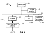
- FIG. 3 is a schematic depiction of a system in accordance with one embodiment of the present invention.
- a phase change memory 10 may be both electrically and optically accessed.
- accessed it is intended to refer to one or more of erasing, reading, and programming.
- a phase change memory cell 14 may be coupled to an addressing circuit 22 .
- the circuit 22 may generate row and column signals that may cause potentials or currents to be applied to the electrodes 16 and 18 .
- the phase change material 24 may function as a variable resistor whose resistance may be optically and electrically altered. In addition, once its resistance has been altered, by passing a current through the variable resistance, the memory cell 14 may be read.
- the circuit 22 may be coupled to logic 26 , in turn coupled to an optical/electrical interface 28 .
- the interface 28 may receive addressing commands from a suitable electronic device. These commands may be converted into an appropriate form by the logic 26 to change the information stored in the memory cell 14 , to either high or low resistance states. These states can then be read out through the circuitry 22 .
- the interface 28 may also develop optical signals that may be used to alter the state of the memory cell 14 .
- an optical mirror system 12 may control the application of laser light to specific cells within the memory cell 14 .
- the system 12 may be a micro-mirror system, so that laser light may be deflected to expose one of a large array of memory cells each having phase change material 24 .
- the memory cell 14 may be covered and protected by an overlying layer 20 .
- the layer 20 may be a transparent layer to permit the passage of light.
- the layer 20 may also thermally insulate the phase change material 24 .
- the array of cells may be arranged in rows and columns, although the terms rows and columns are to some degree arbitrary. Those rows and columns of memory cells may then be electrically accessed, as well as being optically accessed.
- the memory material 24 may be programmed into one of at least two memory states by applying an electrical signal to the memory material.
- An electrical signal may alter the phase of the memory material between a substantially crystalline state and a substantially amorphous state, wherein the electrical resistance of the memory material in the substantially amorphous state is greater than the resistance of the memory material in the substantially crystalline state.
- the memory material 24 may be adapted to be altered to one of at least two resistance values within a range of resistance values to provide single bit or multi-bit storage of information.
- Programming of the memory material 24 to alter the state or phase of the material may be accomplished by applying voltage potentials to the electrodes 16 and 18 , thereby generating a voltage potential across the memory material 24 .
- An electrical current may flow through a portion of the memory material 24 in response to the applied voltage potentials, and may result in heating of the memory material 24 .
- This heating and subsequent cooling may alter the memory state or phase of the memory material 24 .
- Altering the phase or state of the memory material 24 may alter an electrical characteristic of the memory material 24 .
- resistance of the material 24 may be altered by altering the phase of the memory material 24 .
- the memory material 24 may also be referred to as a programmable resistive material or simply a programmable material.
- a voltage potential difference of about 3 volts may be applied across a portion of the memory material 24 by applying about 3 volts to one electrode 16 or 18 and about zero volts to the other electrode 16 or 18 .
- a current flowing through the memory material 24 in response to the applied voltage potentials may result in heating of the memory material. This heating and subsequent cooling may alter the memory state or phase of the material.
- the memory material 24 In a “reset” state, the memory material 24 may be in an amorphous or semi-amorphous state and in a “set” state, the memory material may be in a crystalline or semi-crystalline state.
- the resistance of the memory material in the amorphous or semi-amorphous state may be greater than the resistance of the material in the crystalline or semi-crystalline state.
- the association of reset and set with amorphous and crystalline states, respectively, is a convention. Other conventions may be adopted.
- the memory material may be heated to a relatively higher temperature to amorphisize memory material and “reset” memory material (e.g., program memory material to a logic “0” value). Heating the volume or memory material to a relatively lower crystallization temperature may crystallize memory material and “set” memory material (e.g., program memory material to a logic “1” value).
- Various resistances of memory material may be achieved to store information by varying the amount of current flow and duration through the volume of memory material.
- the information stored in memory material 24 may be read by measuring the resistance of the memory material.
- a read current may be provided to the memory material using opposed electrodes 16 , 18 and a resulting read voltage across the memory material may be compared against a reference voltage using, for example, a sense amplifier (not shown).
- the read voltage may be proportional to the resistance exhibited by the memory storage element.
- a higher voltage may indicate that memory material is in a relatively higher resistance state, e.g., a “reset” state.
- a lower voltage may indicate that the memory material is in a relatively lower resistance state, e.g., a “set” state.
- cells 14 may be coupled to column lines 44 and, through vias 46 , to generally transversely arranged row lines 42 .
- the row lines 42 may be formed below the material 34 , for example, in a semiconductor substrate.
- the column lines 44 may be formed above the material 24 .
- the row lines 42 may extend parallel to one another and may have vias 46 that extend upwardly to contact one of the electrodes 16 or 18 of a cell 14 .
- the other electrode 16 or 18 may be coupled to a column line 42 .
- each memory cell 24 may be arranged in an addressable location, accessible through rows 42 and columns 44 . While an illustrative arrangement is illustrated in FIG. 2 , many other arrangements are also possible.
- phase change material 24 When laser light is deflected through the mirror system 12 to expose a selected cell 14 , localized heating of the phase change material 24 may occur. This heating alters the resistivity of the phase change material 24 as discussed above in connection with electrical heating of the material 24 .
- each cell 14 may act as an optical to electrical transducer.
- information in an optical form may be optically programmed into an array of cells 14 . Then that information may be electrically read out so that optical information has now been converted into electrical information.
- the memory cells 14 are read before they are programmed to determine their present state.
- the cells 14 may be in either a set or reset state depending on their previous programming.
- the optical and electrical systems read the cell 14 to be programmed to know what state it is in at any time.
- the present state of the cell is determined and then the cell is converted into the desired state.
- Optically writing of information in the crystalline state optically may be slower than electrical alteration of the phase change memory into the crystalline state.
- transforming from the amorphous to the crystalline state may advantageously use the electrical programming in some embodiments.
- Light programming may be used when going from the crystalline to the amorphous state in one embodiment of the present invention.
- the programming may be done optically or electrically.
- reading may be done by sensing current by applying a low bias to detect the memory state.
- combinations of optical and electrical programming may be combined with feedback sensing.
- System 500 may be used in wireless devices such as, for example, a personal digital assistant (PDA), a laptop or portable computer with wireless capability, a web tablet, a wireless telephone, a pager, an instant messaging device, a digital music player, a digital camera, or other devices that may be adapted to transmit and/or receive information wirelessly.
- PDA personal digital assistant
- System 500 may be used in any of the following systems: a wireless local area network (WLAN) system, a wireless personal area network (WPAN) system, or a cellular network, although the scope of the present invention is not limited in this respect.
- WLAN wireless local area network
- WPAN wireless personal area network
- cellular network although the scope of the present invention is not limited in this respect.
- System 500 may include a controller 510 , an input/output (I/O) device 520 (e.g. a keypad, display), a memory 530 , and a wireless interface 540 coupled to each other via a bus 550 . It should be noted that the scope of the present invention is not limited to embodiments having any or all of these components.
- I/O input/output
- Controller 510 may comprise, for example, one or more microprocessors, digital signal processors, microcontrollers, or the like.
- Memory 530 may be used to store messages transmitted to or by system 500 .
- Memory 530 may also optionally be used to store instructions that are executed by controller 510 during the operation of system 500 , and may be used to store user data.
- Memory 530 may be provided by one or more different types of memory.
- memory 530 may comprise a volatile memory (any type of random access memory), a non-volatile memory such as a flash memory, and/or phase change memory 10 illustrated in FIG. 1 .
- the I/O device 520 may be used to generate a message.
- the system 500 may use the wireless interface 540 to transmit and receive messages to and from a wireless communication network with a radio frequency (RF) signal.
- RF radio frequency
- Examples of the wireless interface 540 may include an antenna, or a wireless transceiver, such as a dipole antenna, although the scope of the present invention is not limited in this respect.
- An optical network interface 560 may include one or more of the components 12 , 28 , and 26 , shown in FIG. 1 .
- the optical network interface receives a light signal and provides it in an appropriate format to the memory 530 , in one embodiment of the present invention.
Abstract
Description
Claims (10)
Priority Applications (1)
| Application Number | Priority Date | Filing Date | Title |
|---|---|---|---|
| US10/634,146 US7596016B2 (en) | 2003-08-04 | 2003-08-04 | Optically accessible phase change memory |
Applications Claiming Priority (1)
| Application Number | Priority Date | Filing Date | Title |
|---|---|---|---|
| US10/634,146 US7596016B2 (en) | 2003-08-04 | 2003-08-04 | Optically accessible phase change memory |
Publications (2)
| Publication Number | Publication Date |
|---|---|
| US20050030784A1 US20050030784A1 (en) | 2005-02-10 |
| US7596016B2 true US7596016B2 (en) | 2009-09-29 |
Family
ID=34115984
Family Applications (1)
| Application Number | Title | Priority Date | Filing Date |
|---|---|---|---|
| US10/634,146 Active 2027-07-26 US7596016B2 (en) | 2003-08-04 | 2003-08-04 | Optically accessible phase change memory |
Country Status (1)
| Country | Link |
|---|---|
| US (1) | US7596016B2 (en) |
Cited By (3)
| Publication number | Priority date | Publication date | Assignee | Title |
|---|---|---|---|---|
| US20110242873A1 (en) * | 2010-03-31 | 2011-10-06 | Bratkovski Alexandre M | Photo-Responsive Memory Resistor and Method of Operation |
| US10302973B2 (en) | 2015-04-23 | 2019-05-28 | Halliburton Energy Services, Inc. | Spectrally programmable memristor |
| US10591634B2 (en) | 2015-04-23 | 2020-03-17 | Halliburton Energy Services, Inc. | Spectrally programmable memristor-based optical computing |
Families Citing this family (7)
| Publication number | Priority date | Publication date | Assignee | Title |
|---|---|---|---|---|
| US7382512B2 (en) * | 2005-10-26 | 2008-06-03 | Zhizhang Chen | Resistivity phase change material |
| US9293197B2 (en) | 2011-08-15 | 2016-03-22 | Lockheed Martin Corporation | Reconfigurable phase change material masks for electro-optical compressive sensing |
| US9340446B1 (en) | 2013-02-04 | 2016-05-17 | Lockheed Martin Corporation | Optical apparatus and method of forming a gradient index device |
| GB2525184B (en) | 2014-04-14 | 2018-12-19 | Pragmatic Printing Ltd | Electronic Circuit |
| US10437083B1 (en) | 2014-10-20 | 2019-10-08 | Lockheed Martin Corporation | Individually addressable infrared mask array |
| US9969647B2 (en) | 2016-05-17 | 2018-05-15 | Lockheed Martin Energy, Llc | Glass composites having a gradient index of refraction and methods for production thereof |
| US9908808B1 (en) | 2016-08-18 | 2018-03-06 | Lockheed Martin Corporation | Ternary glass materials with low refractive index variability |
Citations (13)
| Publication number | Priority date | Publication date | Assignee | Title |
|---|---|---|---|---|
| US3778785A (en) * | 1972-04-20 | 1973-12-11 | Ibm | Method for writing information at nanosecond speeds and a memory system therefor |
| US4795657A (en) * | 1984-04-13 | 1989-01-03 | Energy Conversion Devices, Inc. | Method of fabricating a programmable array |
| US5206829A (en) * | 1990-10-24 | 1993-04-27 | Sarita Thakoor | Thin film ferroelectric electro-optic memory |
| US5335219A (en) * | 1991-01-18 | 1994-08-02 | Ovshinsky Stanford R | Homogeneous composition of microcrystalline semiconductor material, semiconductor devices and directly overwritable memory elements fabricated therefrom, and arrays fabricated from the memory elements |
| US6005791A (en) * | 1996-06-12 | 1999-12-21 | Gudesen; Hans Gude | Optical logic element and optical logic device |
| US20030128646A1 (en) * | 2002-01-09 | 2003-07-10 | Peter Nangle | Asymmetrical programming mechanism for non-volatile memory |
| US6850432B2 (en) * | 2002-08-20 | 2005-02-01 | Macronix International Co., Ltd. | Laser programmable electrically readable phase-change memory method and device |
| US20050029503A1 (en) * | 2003-08-04 | 2005-02-10 | Johnson Brian G. | Lateral phase change memory |
| US6864503B2 (en) * | 2002-08-09 | 2005-03-08 | Macronix International Co., Ltd. | Spacer chalcogenide memory method and device |
| US6867425B2 (en) * | 2002-12-13 | 2005-03-15 | Intel Corporation | Lateral phase change memory and method therefor |
| US6914255B2 (en) * | 2003-08-04 | 2005-07-05 | Ovonyx, Inc. | Phase change access device for memories |
| US6969867B2 (en) * | 2003-03-10 | 2005-11-29 | Energy Conversion Devices, Inc. | Field effect chalcogenide devices |
| US7106622B2 (en) * | 2002-01-09 | 2006-09-12 | Intel Corporation | Phase-change memory device capable of preprogramming memory cells optically and reading/writing memory cells electrically |
-
2003
- 2003-08-04 US US10/634,146 patent/US7596016B2/en active Active
Patent Citations (14)
| Publication number | Priority date | Publication date | Assignee | Title |
|---|---|---|---|---|
| US3778785A (en) * | 1972-04-20 | 1973-12-11 | Ibm | Method for writing information at nanosecond speeds and a memory system therefor |
| US4795657A (en) * | 1984-04-13 | 1989-01-03 | Energy Conversion Devices, Inc. | Method of fabricating a programmable array |
| US5206829A (en) * | 1990-10-24 | 1993-04-27 | Sarita Thakoor | Thin film ferroelectric electro-optic memory |
| US5335219A (en) * | 1991-01-18 | 1994-08-02 | Ovshinsky Stanford R | Homogeneous composition of microcrystalline semiconductor material, semiconductor devices and directly overwritable memory elements fabricated therefrom, and arrays fabricated from the memory elements |
| US6005791A (en) * | 1996-06-12 | 1999-12-21 | Gudesen; Hans Gude | Optical logic element and optical logic device |
| US20030128646A1 (en) * | 2002-01-09 | 2003-07-10 | Peter Nangle | Asymmetrical programming mechanism for non-volatile memory |
| US7106622B2 (en) * | 2002-01-09 | 2006-09-12 | Intel Corporation | Phase-change memory device capable of preprogramming memory cells optically and reading/writing memory cells electrically |
| US6864503B2 (en) * | 2002-08-09 | 2005-03-08 | Macronix International Co., Ltd. | Spacer chalcogenide memory method and device |
| US6850432B2 (en) * | 2002-08-20 | 2005-02-01 | Macronix International Co., Ltd. | Laser programmable electrically readable phase-change memory method and device |
| US6867425B2 (en) * | 2002-12-13 | 2005-03-15 | Intel Corporation | Lateral phase change memory and method therefor |
| US6969867B2 (en) * | 2003-03-10 | 2005-11-29 | Energy Conversion Devices, Inc. | Field effect chalcogenide devices |
| US6914255B2 (en) * | 2003-08-04 | 2005-07-05 | Ovonyx, Inc. | Phase change access device for memories |
| US20050029503A1 (en) * | 2003-08-04 | 2005-02-10 | Johnson Brian G. | Lateral phase change memory |
| US7161167B2 (en) * | 2003-08-04 | 2007-01-09 | Intel Corporation | Lateral phase change memory |
Non-Patent Citations (4)
| Title |
|---|
| Ha, Y.H., Yi, J.H., Horii, H., Park, J.H., Joo, S.H., Park, S.O., Chung, U-In and Moon, J.T., "An Edge Contact Type Cell for Phase Change RAM Featuring Very Low Power Consumption," presented at IEEE 2003 Symposium on VLSI Technology, Kyoto, Japan, Jun. 12-14, 2003. |
| Horii, H., Yi, J.H., Park, J.H., Ha, Y.H., Baek, I.G., Park, S.O., Hwang, Y.N., Lee, S.H., Kim, Y.T., Lee, K.H., Chung, U-In and Moon, J.T., "A Novel Cell Technology Using N-doped GeSbTe Films for Phase Change RAM," presented at IEEE 2003 Symposium on VLSI Technology, Kyoto, Japan, Jun. 12-14, 2003. |
| Hwang, Y.N., Hong, J.S., Lee, S.H., Ahn, S.J., Jeong, G.T., Koh, G.H., Kim, H.J., Jeong, W.C., Lee, S.Y., Park, J.H., Ryoo, K.C.., Horii, H., Ha, Y.H., Yi, J.H., Cho, W.Y., Kim, Y.T., Lee, K.H., Joo, S.H., Park, S.O., Jeong, U.I., Jeong, H.S. and Kim, Kinam, "Completely CMOS-Compatible Phase-Change Nonvolatile RAM Using NMOS Cell Transistors," presented at 2003 19th IEEE Non-Volatile Semiconductor Memory Workshop, Monterey, California, Feb. 20-26, 2003. |
| Hwang, Y.N., Hong, J.S., Lee, S.H., Ahn, S.J., Jeong, G.T., Koh, G.H., Oh, J.H., Kim, H.J., Jeong, W.C., Lee, S.Y., Park, J.H., Ryoo, K.C., Horii, H., Ha, Y.H., Yi, J.H., Cho, W.Y., Kim, Y.T., Lee, K.H., Joo, S.H., Park, S.O., Chung, U.I., Jeong, H.S. and Kim, Kinam, "Full Integration and Reliability Evaluation of Phase-change RAM Based on 0.24 mm-CMOS Technologies," presented at IEEE 2003 Symposium on VLSI Technology, Kyoto, Japan, Jun. 12-14, 2003. |
Cited By (4)
| Publication number | Priority date | Publication date | Assignee | Title |
|---|---|---|---|---|
| US20110242873A1 (en) * | 2010-03-31 | 2011-10-06 | Bratkovski Alexandre M | Photo-Responsive Memory Resistor and Method of Operation |
| US8542518B2 (en) * | 2010-03-31 | 2013-09-24 | Hewlett-Packard Development Company, L.P. | Photo-responsive memory resistor and method of operation |
| US10302973B2 (en) | 2015-04-23 | 2019-05-28 | Halliburton Energy Services, Inc. | Spectrally programmable memristor |
| US10591634B2 (en) | 2015-04-23 | 2020-03-17 | Halliburton Energy Services, Inc. | Spectrally programmable memristor-based optical computing |
Also Published As
| Publication number | Publication date |
|---|---|
| US20050030784A1 (en) | 2005-02-10 |
Similar Documents
| Publication | Publication Date | Title |
|---|---|---|
| KR100704329B1 (en) | Using a phase change memory as a replacement for a buffered flash memory | |
| TWI327730B (en) | Analog phase change memory | |
| KR100796430B1 (en) | Phase change access device for memories | |
| US7359231B2 (en) | Providing current for phase change memories | |
| US8750066B2 (en) | Temperature compensation of conductive bridge memory arrays | |
| KR101126846B1 (en) | Semiconductor memory device and semiconductor device | |
| US7381611B2 (en) | Multilayered phase change memory | |
| US9318194B1 (en) | Apparatus and methods for sensing hard bit and soft bits | |
| US8113437B2 (en) | RFID device with memory unit having memristor characteristics | |
| US7804082B2 (en) | Phase change memory system | |
| US8050083B2 (en) | Phase change memory device and write method thereof | |
| US9361977B2 (en) | Reliable read operation for nonvolatile memory device with resistance material that reads data based on reference current | |
| KR100866657B1 (en) | Read bias scheme for phase change memories | |
| US8570795B2 (en) | Adaptive wordline programming bias of a phase change memory | |
| KR20030045639A (en) | Write current compensation for temperature variations in memory arrays | |
| US7596016B2 (en) | Optically accessible phase change memory | |
| KR20140054715A (en) | Nonvolatile memory device using variable resistive element and driving method thereof | |
| CN111566739B (en) | Techniques for updating trimming parameters in non-volatile memory | |
| KR20150116513A (en) | Nonvolatile memory device and memory system including the same | |
| WO2006031503A1 (en) | One time programmable phase change memory | |
| KR20190141975A (en) | Resistive memory device comprising compensation circuit | |
| US20070238225A1 (en) | Phase change memory with improved temperature stability | |
| US20060056234A1 (en) | Using a phase change memory as a shadow RAM | |
| US20050029504A1 (en) | Reducing parasitic conductive paths in phase change memories | |
| EP1626411A1 (en) | Shared address lines for crosspoint memory |
Legal Events
| Date | Code | Title | Description |
|---|---|---|---|
| AS | Assignment |
Owner name: OVONYX, INC., IDAHO Free format text: ASSIGNMENT OF ASSIGNORS INTEREST;ASSIGNOR:JOHNSON, BRIAN G.;REEL/FRAME:014767/0213 Effective date: 20031113 |
|
| STCF | Information on status: patent grant |
Free format text: PATENTED CASE |
|
| CC | Certificate of correction | ||
| FEPP | Fee payment procedure |
Free format text: PAYOR NUMBER ASSIGNED (ORIGINAL EVENT CODE: ASPN); ENTITY STATUS OF PATENT OWNER: LARGE ENTITY |
|
| FPAY | Fee payment |
Year of fee payment: 4 |
|
| AS | Assignment |
Owner name: CARLOW INNOVATIONS LLC, VIRGINIA Free format text: ASSIGNMENT OF ASSIGNORS INTEREST;ASSIGNOR:OVONYX, INC.;REEL/FRAME:037244/0954 Effective date: 20150731 |
|
| AS | Assignment |
Owner name: OVONYX MEMORY TECHNOLOGY, LLC, VIRGINIA Free format text: CHANGE OF NAME;ASSIGNOR:CARLOW INNOVATIONS, LLC;REEL/FRAME:039379/0077 Effective date: 20160708 |
|
| FPAY | Fee payment |
Year of fee payment: 8 |
|
| FEPP | Fee payment procedure |
Free format text: MAINTENANCE FEE REMINDER MAILED (ORIGINAL EVENT CODE: REM.); ENTITY STATUS OF PATENT OWNER: LARGE ENTITY |
|
| FEPP | Fee payment procedure |
Free format text: 11.5 YR SURCHARGE- LATE PMT W/IN 6 MO, LARGE ENTITY (ORIGINAL EVENT CODE: M1556); ENTITY STATUS OF PATENT OWNER: LARGE ENTITY |
|
| MAFP | Maintenance fee payment |
Free format text: PAYMENT OF MAINTENANCE FEE, 12TH YEAR, LARGE ENTITY (ORIGINAL EVENT CODE: M1553); ENTITY STATUS OF PATENT OWNER: LARGE ENTITY Year of fee payment: 12 |