US7598607B2 - Semiconductor packages with enhanced joint reliability and methods of fabricating the same - Google Patents
Semiconductor packages with enhanced joint reliability and methods of fabricating the same Download PDFInfo
- Publication number
- US7598607B2 US7598607B2 US12/123,367 US12336708A US7598607B2 US 7598607 B2 US7598607 B2 US 7598607B2 US 12336708 A US12336708 A US 12336708A US 7598607 B2 US7598607 B2 US 7598607B2
- Authority
- US
- United States
- Prior art keywords
- package
- top layer
- substrate
- semiconductor
- bottom layer
- Prior art date
- Legal status (The legal status is an assumption and is not a legal conclusion. Google has not performed a legal analysis and makes no representation as to the accuracy of the status listed.)
- Active
Links
Images


Classifications
-
- H—ELECTRICITY
- H01—ELECTRIC ELEMENTS
- H01L—SEMICONDUCTOR DEVICES NOT COVERED BY CLASS H10
- H01L23/00—Details of semiconductor or other solid state devices
- H01L23/28—Encapsulations, e.g. encapsulating layers, coatings, e.g. for protection
- H01L23/31—Encapsulations, e.g. encapsulating layers, coatings, e.g. for protection characterised by the arrangement or shape
- H01L23/3107—Encapsulations, e.g. encapsulating layers, coatings, e.g. for protection characterised by the arrangement or shape the device being completely enclosed
- H01L23/3121—Encapsulations, e.g. encapsulating layers, coatings, e.g. for protection characterised by the arrangement or shape the device being completely enclosed a substrate forming part of the encapsulation
- H01L23/3128—Encapsulations, e.g. encapsulating layers, coatings, e.g. for protection characterised by the arrangement or shape the device being completely enclosed a substrate forming part of the encapsulation the substrate having spherical bumps for external connection
-
- H—ELECTRICITY
- H01—ELECTRIC ELEMENTS
- H01L—SEMICONDUCTOR DEVICES NOT COVERED BY CLASS H10
- H01L23/00—Details of semiconductor or other solid state devices
- H01L23/28—Encapsulations, e.g. encapsulating layers, coatings, e.g. for protection
-
- H—ELECTRICITY
- H01—ELECTRIC ELEMENTS
- H01L—SEMICONDUCTOR DEVICES NOT COVERED BY CLASS H10
- H01L23/00—Details of semiconductor or other solid state devices
- H01L23/12—Mountings, e.g. non-detachable insulating substrates
-
- H—ELECTRICITY
- H01—ELECTRIC ELEMENTS
- H01L—SEMICONDUCTOR DEVICES NOT COVERED BY CLASS H10
- H01L23/00—Details of semiconductor or other solid state devices
- H01L23/52—Arrangements for conducting electric current within the device in operation from one component to another, i.e. interconnections, e.g. wires, lead frames
- H01L23/538—Arrangements for conducting electric current within the device in operation from one component to another, i.e. interconnections, e.g. wires, lead frames the interconnection structure between a plurality of semiconductor chips being formed on, or in, insulating substrates
- H01L23/5389—Arrangements for conducting electric current within the device in operation from one component to another, i.e. interconnections, e.g. wires, lead frames the interconnection structure between a plurality of semiconductor chips being formed on, or in, insulating substrates the chips being integrally enclosed by the interconnect and support structures
-
- H—ELECTRICITY
- H01—ELECTRIC ELEMENTS
- H01L—SEMICONDUCTOR DEVICES NOT COVERED BY CLASS H10
- H01L24/00—Arrangements for connecting or disconnecting semiconductor or solid-state bodies; Methods or apparatus related thereto
- H01L24/01—Means for bonding being attached to, or being formed on, the surface to be connected, e.g. chip-to-package, die-attach, "first-level" interconnects; Manufacturing methods related thereto
- H01L24/18—High density interconnect [HDI] connectors; Manufacturing methods related thereto
- H01L24/23—Structure, shape, material or disposition of the high density interconnect connectors after the connecting process
- H01L24/24—Structure, shape, material or disposition of the high density interconnect connectors after the connecting process of an individual high density interconnect connector
-
- H—ELECTRICITY
- H01—ELECTRIC ELEMENTS
- H01L—SEMICONDUCTOR DEVICES NOT COVERED BY CLASS H10
- H01L25/00—Assemblies consisting of a plurality of individual semiconductor or other solid state devices ; Multistep manufacturing processes thereof
- H01L25/03—Assemblies consisting of a plurality of individual semiconductor or other solid state devices ; Multistep manufacturing processes thereof all the devices being of a type provided for in the same subgroup of groups H01L27/00 - H01L33/00, or in a single subclass of H10K, H10N, e.g. assemblies of rectifier diodes
- H01L25/10—Assemblies consisting of a plurality of individual semiconductor or other solid state devices ; Multistep manufacturing processes thereof all the devices being of a type provided for in the same subgroup of groups H01L27/00 - H01L33/00, or in a single subclass of H10K, H10N, e.g. assemblies of rectifier diodes the devices having separate containers
- H01L25/105—Assemblies consisting of a plurality of individual semiconductor or other solid state devices ; Multistep manufacturing processes thereof all the devices being of a type provided for in the same subgroup of groups H01L27/00 - H01L33/00, or in a single subclass of H10K, H10N, e.g. assemblies of rectifier diodes the devices having separate containers the devices being of a type provided for in group H01L27/00
-
- H—ELECTRICITY
- H01—ELECTRIC ELEMENTS
- H01L—SEMICONDUCTOR DEVICES NOT COVERED BY CLASS H10
- H01L2224/00—Indexing scheme for arrangements for connecting or disconnecting semiconductor or solid-state bodies and methods related thereto as covered by H01L24/00
- H01L2224/01—Means for bonding being attached to, or being formed on, the surface to be connected, e.g. chip-to-package, die-attach, "first-level" interconnects; Manufacturing methods related thereto
- H01L2224/18—High density interconnect [HDI] connectors; Manufacturing methods related thereto
- H01L2224/23—Structure, shape, material or disposition of the high density interconnect connectors after the connecting process
- H01L2224/24—Structure, shape, material or disposition of the high density interconnect connectors after the connecting process of an individual high density interconnect connector
- H01L2224/241—Disposition
- H01L2224/24151—Connecting between a semiconductor or solid-state body and an item not being a semiconductor or solid-state body, e.g. chip-to-substrate, chip-to-passive
- H01L2224/24221—Connecting between a semiconductor or solid-state body and an item not being a semiconductor or solid-state body, e.g. chip-to-substrate, chip-to-passive the body and the item being stacked
- H01L2224/24225—Connecting between a semiconductor or solid-state body and an item not being a semiconductor or solid-state body, e.g. chip-to-substrate, chip-to-passive the body and the item being stacked the item being non-metallic, e.g. insulating substrate with or without metallisation
- H01L2224/24226—Connecting between a semiconductor or solid-state body and an item not being a semiconductor or solid-state body, e.g. chip-to-substrate, chip-to-passive the body and the item being stacked the item being non-metallic, e.g. insulating substrate with or without metallisation the HDI interconnect connecting to the same level of the item at which the semiconductor or solid-state body is mounted, e.g. the item being planar
-
- H—ELECTRICITY
- H01—ELECTRIC ELEMENTS
- H01L—SEMICONDUCTOR DEVICES NOT COVERED BY CLASS H10
- H01L2224/00—Indexing scheme for arrangements for connecting or disconnecting semiconductor or solid-state bodies and methods related thereto as covered by H01L24/00
- H01L2224/01—Means for bonding being attached to, or being formed on, the surface to be connected, e.g. chip-to-package, die-attach, "first-level" interconnects; Manufacturing methods related thereto
- H01L2224/26—Layer connectors, e.g. plate connectors, solder or adhesive layers; Manufacturing methods related thereto
- H01L2224/31—Structure, shape, material or disposition of the layer connectors after the connecting process
- H01L2224/32—Structure, shape, material or disposition of the layer connectors after the connecting process of an individual layer connector
- H01L2224/321—Disposition
- H01L2224/32151—Disposition the layer connector connecting between a semiconductor or solid-state body and an item not being a semiconductor or solid-state body, e.g. chip-to-substrate, chip-to-passive
- H01L2224/32221—Disposition the layer connector connecting between a semiconductor or solid-state body and an item not being a semiconductor or solid-state body, e.g. chip-to-substrate, chip-to-passive the body and the item being stacked
- H01L2224/32225—Disposition the layer connector connecting between a semiconductor or solid-state body and an item not being a semiconductor or solid-state body, e.g. chip-to-substrate, chip-to-passive the body and the item being stacked the item being non-metallic, e.g. insulating substrate with or without metallisation
-
- H—ELECTRICITY
- H01—ELECTRIC ELEMENTS
- H01L—SEMICONDUCTOR DEVICES NOT COVERED BY CLASS H10
- H01L2224/00—Indexing scheme for arrangements for connecting or disconnecting semiconductor or solid-state bodies and methods related thereto as covered by H01L24/00
- H01L2224/73—Means for bonding being of different types provided for in two or more of groups H01L2224/10, H01L2224/18, H01L2224/26, H01L2224/34, H01L2224/42, H01L2224/50, H01L2224/63, H01L2224/71
- H01L2224/732—Location after the connecting process
- H01L2224/73251—Location after the connecting process on different surfaces
- H01L2224/73267—Layer and HDI connectors
-
- H—ELECTRICITY
- H01—ELECTRIC ELEMENTS
- H01L—SEMICONDUCTOR DEVICES NOT COVERED BY CLASS H10
- H01L2224/00—Indexing scheme for arrangements for connecting or disconnecting semiconductor or solid-state bodies and methods related thereto as covered by H01L24/00
- H01L2224/80—Methods for connecting semiconductor or other solid state bodies using means for bonding being attached to, or being formed on, the surface to be connected
- H01L2224/82—Methods for connecting semiconductor or other solid state bodies using means for bonding being attached to, or being formed on, the surface to be connected by forming build-up interconnects at chip-level, e.g. for high density interconnects [HDI]
- H01L2224/82009—Pre-treatment of the connector or the bonding area
- H01L2224/8203—Reshaping, e.g. forming vias
- H01L2224/82035—Reshaping, e.g. forming vias by heating means
- H01L2224/82039—Reshaping, e.g. forming vias by heating means using a laser
-
- H—ELECTRICITY
- H01—ELECTRIC ELEMENTS
- H01L—SEMICONDUCTOR DEVICES NOT COVERED BY CLASS H10
- H01L2224/00—Indexing scheme for arrangements for connecting or disconnecting semiconductor or solid-state bodies and methods related thereto as covered by H01L24/00
- H01L2224/80—Methods for connecting semiconductor or other solid state bodies using means for bonding being attached to, or being formed on, the surface to be connected
- H01L2224/82—Methods for connecting semiconductor or other solid state bodies using means for bonding being attached to, or being formed on, the surface to be connected by forming build-up interconnects at chip-level, e.g. for high density interconnects [HDI]
- H01L2224/82009—Pre-treatment of the connector or the bonding area
- H01L2224/8203—Reshaping, e.g. forming vias
- H01L2224/82047—Reshaping, e.g. forming vias by mechanical means, e.g. severing, pressing, stamping
-
- H—ELECTRICITY
- H01—ELECTRIC ELEMENTS
- H01L—SEMICONDUCTOR DEVICES NOT COVERED BY CLASS H10
- H01L2224/00—Indexing scheme for arrangements for connecting or disconnecting semiconductor or solid-state bodies and methods related thereto as covered by H01L24/00
- H01L2224/91—Methods for connecting semiconductor or solid state bodies including different methods provided for in two or more of groups H01L2224/80 - H01L2224/90
- H01L2224/92—Specific sequence of method steps
- H01L2224/922—Connecting different surfaces of the semiconductor or solid-state body with connectors of different types
- H01L2224/9222—Sequential connecting processes
- H01L2224/92242—Sequential connecting processes the first connecting process involving a layer connector
- H01L2224/92244—Sequential connecting processes the first connecting process involving a layer connector the second connecting process involving a build-up interconnect
-
- H—ELECTRICITY
- H01—ELECTRIC ELEMENTS
- H01L—SEMICONDUCTOR DEVICES NOT COVERED BY CLASS H10
- H01L2225/00—Details relating to assemblies covered by the group H01L25/00 but not provided for in its subgroups
- H01L2225/03—All the devices being of a type provided for in the same subgroup of groups H01L27/00 - H01L33/648 and H10K99/00
- H01L2225/10—All the devices being of a type provided for in the same subgroup of groups H01L27/00 - H01L33/648 and H10K99/00 the devices having separate containers
- H01L2225/1005—All the devices being of a type provided for in the same subgroup of groups H01L27/00 - H01L33/648 and H10K99/00 the devices having separate containers the devices being of a type provided for in group H01L27/00
- H01L2225/1011—All the devices being of a type provided for in the same subgroup of groups H01L27/00 - H01L33/648 and H10K99/00 the devices having separate containers the devices being of a type provided for in group H01L27/00 the containers being in a stacked arrangement
- H01L2225/1017—All the devices being of a type provided for in the same subgroup of groups H01L27/00 - H01L33/648 and H10K99/00 the devices having separate containers the devices being of a type provided for in group H01L27/00 the containers being in a stacked arrangement the lowermost container comprising a device support
- H01L2225/1035—All the devices being of a type provided for in the same subgroup of groups H01L27/00 - H01L33/648 and H10K99/00 the devices having separate containers the devices being of a type provided for in group H01L27/00 the containers being in a stacked arrangement the lowermost container comprising a device support the device being entirely enclosed by the support, e.g. high-density interconnect [HDI]
-
- H—ELECTRICITY
- H01—ELECTRIC ELEMENTS
- H01L—SEMICONDUCTOR DEVICES NOT COVERED BY CLASS H10
- H01L2225/00—Details relating to assemblies covered by the group H01L25/00 but not provided for in its subgroups
- H01L2225/03—All the devices being of a type provided for in the same subgroup of groups H01L27/00 - H01L33/648 and H10K99/00
- H01L2225/10—All the devices being of a type provided for in the same subgroup of groups H01L27/00 - H01L33/648 and H10K99/00 the devices having separate containers
- H01L2225/1005—All the devices being of a type provided for in the same subgroup of groups H01L27/00 - H01L33/648 and H10K99/00 the devices having separate containers the devices being of a type provided for in group H01L27/00
- H01L2225/1011—All the devices being of a type provided for in the same subgroup of groups H01L27/00 - H01L33/648 and H10K99/00 the devices having separate containers the devices being of a type provided for in group H01L27/00 the containers being in a stacked arrangement
- H01L2225/1047—Details of electrical connections between containers
- H01L2225/1058—Bump or bump-like electrical connections, e.g. balls, pillars, posts
-
- H—ELECTRICITY
- H01—ELECTRIC ELEMENTS
- H01L—SEMICONDUCTOR DEVICES NOT COVERED BY CLASS H10
- H01L2924/00—Indexing scheme for arrangements or methods for connecting or disconnecting semiconductor or solid-state bodies as covered by H01L24/00
- H01L2924/01—Chemical elements
- H01L2924/01005—Boron [B]
-
- H—ELECTRICITY
- H01—ELECTRIC ELEMENTS
- H01L—SEMICONDUCTOR DEVICES NOT COVERED BY CLASS H10
- H01L2924/00—Indexing scheme for arrangements or methods for connecting or disconnecting semiconductor or solid-state bodies as covered by H01L24/00
- H01L2924/01—Chemical elements
- H01L2924/01006—Carbon [C]
-
- H—ELECTRICITY
- H01—ELECTRIC ELEMENTS
- H01L—SEMICONDUCTOR DEVICES NOT COVERED BY CLASS H10
- H01L2924/00—Indexing scheme for arrangements or methods for connecting or disconnecting semiconductor or solid-state bodies as covered by H01L24/00
- H01L2924/01—Chemical elements
- H01L2924/01033—Arsenic [As]
-
- H—ELECTRICITY
- H01—ELECTRIC ELEMENTS
- H01L—SEMICONDUCTOR DEVICES NOT COVERED BY CLASS H10
- H01L2924/00—Indexing scheme for arrangements or methods for connecting or disconnecting semiconductor or solid-state bodies as covered by H01L24/00
- H01L2924/01—Chemical elements
- H01L2924/01038—Strontium [Sr]
-
- H—ELECTRICITY
- H01—ELECTRIC ELEMENTS
- H01L—SEMICONDUCTOR DEVICES NOT COVERED BY CLASS H10
- H01L2924/00—Indexing scheme for arrangements or methods for connecting or disconnecting semiconductor or solid-state bodies as covered by H01L24/00
- H01L2924/01—Chemical elements
- H01L2924/01047—Silver [Ag]
-
- H—ELECTRICITY
- H01—ELECTRIC ELEMENTS
- H01L—SEMICONDUCTOR DEVICES NOT COVERED BY CLASS H10
- H01L2924/00—Indexing scheme for arrangements or methods for connecting or disconnecting semiconductor or solid-state bodies as covered by H01L24/00
- H01L2924/01—Chemical elements
- H01L2924/01074—Tungsten [W]
-
- H—ELECTRICITY
- H01—ELECTRIC ELEMENTS
- H01L—SEMICONDUCTOR DEVICES NOT COVERED BY CLASS H10
- H01L2924/00—Indexing scheme for arrangements or methods for connecting or disconnecting semiconductor or solid-state bodies as covered by H01L24/00
- H01L2924/01—Chemical elements
- H01L2924/01078—Platinum [Pt]
-
- H—ELECTRICITY
- H01—ELECTRIC ELEMENTS
- H01L—SEMICONDUCTOR DEVICES NOT COVERED BY CLASS H10
- H01L2924/00—Indexing scheme for arrangements or methods for connecting or disconnecting semiconductor or solid-state bodies as covered by H01L24/00
- H01L2924/10—Details of semiconductor or other solid state devices to be connected
- H01L2924/11—Device type
- H01L2924/14—Integrated circuits
-
- H—ELECTRICITY
- H01—ELECTRIC ELEMENTS
- H01L—SEMICONDUCTOR DEVICES NOT COVERED BY CLASS H10
- H01L2924/00—Indexing scheme for arrangements or methods for connecting or disconnecting semiconductor or solid-state bodies as covered by H01L24/00
- H01L2924/15—Details of package parts other than the semiconductor or other solid state devices to be connected
- H01L2924/151—Die mounting substrate
- H01L2924/153—Connection portion
- H01L2924/1531—Connection portion the connection portion being formed only on the surface of the substrate opposite to the die mounting surface
- H01L2924/15311—Connection portion the connection portion being formed only on the surface of the substrate opposite to the die mounting surface being a ball array, e.g. BGA
-
- H—ELECTRICITY
- H01—ELECTRIC ELEMENTS
- H01L—SEMICONDUCTOR DEVICES NOT COVERED BY CLASS H10
- H01L2924/00—Indexing scheme for arrangements or methods for connecting or disconnecting semiconductor or solid-state bodies as covered by H01L24/00
- H01L2924/15—Details of package parts other than the semiconductor or other solid state devices to be connected
- H01L2924/151—Die mounting substrate
- H01L2924/153—Connection portion
- H01L2924/1532—Connection portion the connection portion being formed on the die mounting surface of the substrate
- H01L2924/1533—Connection portion the connection portion being formed on the die mounting surface of the substrate the connection portion being formed both on the die mounting surface of the substrate and outside the die mounting surface of the substrate
- H01L2924/15331—Connection portion the connection portion being formed on the die mounting surface of the substrate the connection portion being formed both on the die mounting surface of the substrate and outside the die mounting surface of the substrate being a ball array, e.g. BGA
-
- H—ELECTRICITY
- H01—ELECTRIC ELEMENTS
- H01L—SEMICONDUCTOR DEVICES NOT COVERED BY CLASS H10
- H01L2924/00—Indexing scheme for arrangements or methods for connecting or disconnecting semiconductor or solid-state bodies as covered by H01L24/00
- H01L2924/30—Technical effects
- H01L2924/301—Electrical effects
- H01L2924/3011—Impedance
-
- H—ELECTRICITY
- H01—ELECTRIC ELEMENTS
- H01L—SEMICONDUCTOR DEVICES NOT COVERED BY CLASS H10
- H01L2924/00—Indexing scheme for arrangements or methods for connecting or disconnecting semiconductor or solid-state bodies as covered by H01L24/00
- H01L2924/30—Technical effects
- H01L2924/35—Mechanical effects
- H01L2924/351—Thermal stress
Definitions
- the present invention disclosed herein relates to a semiconductor package and a method of fabricating the same, and more particularly, to a semiconductor package with enhanced joint reliability and methods of fabricating the same.
- semiconductor device fabrication include a front-end process in which integrated circuit (IC) chips are formed on a wafer through photolithography, deposition, and etching processes, and a back-end process that assembles and packages each of the IC chips.
- IC integrated circuit
- POP package-on-package
- CSP chip scale packaging
- WLP wafer-level packaging
- the 3-D stacking technology can drastically reduce the interconnection length between chips, it is considered to be a method capable of overcoming technical limitations such as signal delay and power consumption. Furthermore, the 3-D stacking technology provides improved technical aspects including electrical characteristics, form factor, size and density.
- a semiconductor package which is manufactured through a typical 3-D stacking technology, is vulnerable to thermal stress caused by heat generated from a semiconductor chip or supplied during a manufacturing process, or a mechanical stress caused due to an external force.
- thermal or mechanical stress is concentrated on bumps that connect semiconductor chips electrically, the bumps may be damaged.
- joint reliability of a package structure may be deteriorated.
- the present invention provides a semiconductor package with enhanced joint reliability and methods of fabricating the same.
- a semiconductor package includes: a substrate; and at least one package unit stacked on the substrate, each of the package units including a semiconductor chip having a pad, a bottom layer and a top layer substantially surrounding the semiconductor chip, and a redistribution structure overlying the top layer.
- the redistribution structure is electrically connected to the pad.
- the top layer and the bottom layer have a lower modulus than the redistribution structure and the semiconductor chip.
- FIGS. 1 through 6 are cross-sectional views illustrating a method of fabricating a semiconductor package according to an embodiment of the present invention
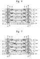
- FIGS. 7 and 8 are cross-sectional views illustrating a method of fabricating a semiconductor package according to other embodiments of the present invention.
- FIGS. 9 and 10 are cross-sectional views illustrating semiconductor packages and a method of fabricating the same according to the present invention.
- FIGS. 1 through 6 are cross-sectional views illustrating a method of fabricating a semiconductor package according to an embodiment of the present invention.
- a semiconductor chip 20 is attached on a bottom layer 10 .
- the semiconductor chip 20 includes at least one input/output pad (hereinafter, referred to as a pad) 25 connected to an internal circuit, and the position of the pad 25 may vary according to the design of the semiconductor chip 20 .
- the semiconductor chip 20 is manufactured through a front-end process, and a plurality of semiconductor chips may be attached on one bottom layer.
- the semiconductor chip 20 may be, for example, a memory chip or a logic circuit chip.
- the bottom layer 10 may be formed of a material having a lower modulus than the semiconductor chip 20 .
- the bottom layer 10 may be formed of at least one among materials having Young's modulus between about 10 MPa and about 1 GPa. More preferably, the bottom layer 10 is formed of at least one among materials having Young's modulus between about 10 MPa and about 100 MPa.
- the bottom layer 10 may be formed of at least one of silicone compounds, rubber compounds, photosensitive resin compounds, and synthetic resin compounds.
- the thickness t 2 of the semiconductor chip 20 may be between about 10 ⁇ m and about 100 ⁇ m. According to an embodiment, the thickness t 2 of the semiconductor chip 20 may be below about 30 ⁇ m. When the semiconductor chip 20 has such a small thickness, it may be easily deformed by thermal or mechanical stress. However, if the bottom layer 10 is formed of a material with a low modulus, deformation of the semiconductor chip 20 due to an external stress can be reduced. According to the embodiments, the thickness t 1 of the bottom layer 10 ranges from about 5 ⁇ m to about 1000 ⁇ m.
- the semiconductor chip 20 may be attached on the bottom layer 10 without an additional adhesive layer.
- an adhesive layer (not shown) may be further formed between the bottom layer 10 and the semiconductor chip 20 to promote adhesion therebetween.
- a top layer 30 is formed on the bottom layer 10 having the semiconductor chip 20 .
- the semiconductor chip 20 is substantially surround, or sealed, by the top layer 30 and the bottom layer 10 .
- the top layer 30 may be formed of a material having a lower modulus than the semiconductor chip 20 . That is, the top layer 30 may be formed of at least one among materials having Young's modulus between about 10 MPa and about 1 GPa. More preferably, the top layer 30 is formed of at least one among materials having Young's modulus between about 10 MPa and about 100 MPa. Additionally, the top layer 30 may be formed of at least one of silicone compounds, rubber compounds, photosensitive resin compounds, and synthetic resin compounds. According to one embodiment, the top layer 30 may be formed of the same material as the bottom layer 10 . According to another embodiment, the top layer 30 may be formed of a material different from that of the bottom layer 10 .
- the thickness t 1 of the top layer 30 ranges from about 5 ⁇ m to about 1000 ⁇ m.
- the semiconductor chip 20 since the semiconductor chip 20 is sealed by the top layer 30 and the bottom layer 10 of a low modulus material, the deformation of the semiconductor chip 20 due to an external stress may be further reduced, and the probability that the semiconductor chip 20 will be separated from the top layer 30 or the bottom layer 10 is also reduced.
- the semiconductor chip 20 when only one of the bottom layer 10 and the top layer 30 covers the semiconductor chip 20 , the semiconductor chip 20 may be separated from the top layer 30 or the bottom layer 10 because of gravity applied to the semiconductor chip 20 and heat generated in the semiconductor chip 20 and supplied during a manufacturing process.
- the semiconductor chip 20 when the semiconductor chip 20 is sealed by the top layer 30 and the bottom layer 10 , such separation can be effectively prevented.
- the top layer 30 and the bottom layer 10 are patterned to form a via hole 34 penetrating the top layer 30 and the bottom layer 10 and a pad opening part 32 penetrating the top layer 30 to expose the pad 25 .
- the patterning process may be performed using one of a photolithography and etching process, a laser drilling process, a mechanical drilling process, and an ion-beam drilling process.
- the photolithography and etching process includes forming the photoresist pattern for defining the via hole 34 and the pad opening part 32 on the top layer 30 and etching the top layer 30 and the bottom layer 10 by using the photoresist pattern as an etching mask.
- the etching of the top layer 30 may be performed using an etching recipe having an etching selectivity with respect to the pad 25 .
- the via hole 34 and the pad opening part 32 are simultaneously formed.
- the bottom layer 10 and the top layer 30 can be easily etched compared to the semiconductor chip 20 (i.e., a wafer), it is easier to fabricate a semiconductor package compared to a conventional through substrate via (TSV) technology that includes a step of forming a via hole to penetrate the wafer. Because of this ease of etching, the present invention can be used to fabricate a semiconductor package with lower cost, higher reliability, and higher productivity compared to a conventional technology.
- TSV through substrate via
- the via holes 34 may be formed around the semiconductor chip 20 , being spaced apart from the edge of the semiconductor chip 20 . At this point, positions where the via holes 34 are formed may be selected such that the package units are electrically connected to each other during a subsequent step of stacking the package units. That is, the intervals between the via holes 34 and the semiconductor chip 20 and the positions of the via holes 34 may be determined by considering the electrical connections.
- the width of the via holes 34 may range from about 10 ⁇ m to about 100 ⁇ m.
- a redistribution structure 40 which is connected with the exposed top surface of the pad 25 , is formed using a redistribution process.
- the redistribution process forms new interconnections that are electrically connected to the pads 25 of the semiconductor chip 20 to facilitate easy package processing.
- the redistribution structure 40 includes new interconnections used for the above purpose. Specifically, in a case of a package structure including stacked semiconductor chips, the semiconductor chips may be electrically connected through the redistribution structure regardless of the position of the pads 25 . That is, when using the redistribution structure 40 , various and simple connection techniques can be used, because the electrical connection between the semiconductor chips is not limited to the positions of the pads.
- the forming of the redistribution structure 40 further includes a step of forming a mold layer having a mold opening part 32 , which defines the shape of the redistribution structure 40 , on the resultant structure having the via hole 34 and the pad opening part 32 and a step of forming a metal layer using an electroplating technique to fill the mold opening part 32 .
- a seed layer which will be used as a seed electrode during the electroplating step, may be formed before forming the metal layer.
- the seed layer may be formed through a sputtering or evaporation technique.
- the thickness of the mold layer (i.e., the thickness of the redistribution structure 40 ) may be between about 1 ⁇ m and about 50 ⁇ m. More preferably, the thickness of the molder layer is between about 2 ⁇ m and about 10 ⁇ m.
- a method of fabricating the redistribution structure 40 is not limited to the above method, however, and the redistribution structure 40 can be realized through various other methods.
- the fabricating of the redistribution structure 40 may include a step of forming of the seed layer and the metal layer and a step of patterning the metal layer and the seed layer using a photolithography and etching process.
- the redistribution structure 40 is extended from the pad 25 so as to cover an inner wall of the via hole 34 . As shown in FIG. 4 , the redistribution structure 40 might not completely fill the via hole 34 , or may extend a short distance along the bottom surface of the bottom layer 40 . According to another embodiment, although the redistribution structure 40 may cover the inner wall of the via hole 34 , it might not extend along the bottom surface of the bottom layer 10 .
- connecting elements 50 are formed on the redistribution structures 40 .
- the connecting elements 50 may be formed using one of a ball bump jet technique, an electroplating technique, and a bump printing technique.
- the connecting elements 50 may be formed using a process of forming the redistribution structure 40 . That is, the connecting elements 50 and the redistribution structure 40 may be formed using the same process.
- the connecting elements 50 may be formed on the top or the bottom of the via holes 34 .
- the connecting elements 50 extend into the via hole 34 to fill a portion of the via hole 34 , as shown in FIG. 5 .
- a contact area between the connecting element 50 and the redistribution structure 40 increases, such that contact resistance may be reduced.
- the connecting element 50 fills a portion of the via hole 34 , it may be robustly jointed to the redistribution structure 40 .
- the bottom layer 10 and the top layer 30 are formed of a flexible material with a low modulus, a mechanical stress applied to the connecting element 50 may be absorbed into the bottom layer 10 and the top layer 30 through the sidewall of the via hole 34 . Due to this stress absorption, the package structure of this invention provides enhanced joint reliability.
- individual package units 100 are separated by cutting the bottom layer 10 and the top layer 30 through a dicing process.
- the semiconductor chip 20 , the top layer 30 , the bottom layer 10 , the redistribution structure 40 , and the connecting element 50 can be referred to as a package unit 100 .
- the dicing process includes cutting the bottom layer 10 and the top layer 30 along a separation region SR around the semiconductor chip 20 .
- the separation region SR may be disposed between adjacent semiconductor chips 20 (i.e., between the redistribution structures 40 connected to the respectively different semiconductor chips 20 ).
- the dicing process may be realized using one of a laser, a saw, and a knife.
- the package units 100 separated through the dicing process are sequentially stacked on a substrate 200 (although four package units are illustrated in FIG. 6 , the number of the package units 100 may vary).
- Substrate pads 210 are disposed on the substrate 200 , and the connecting elements 50 of the package units 100 are connected to the substrate pads 210 .
- the package unit 100 and the substrate pads 210 may be connected through a substrate connecting element 55 .
- Connecting terminals (not shown) may be formed on a predetermined region of the substrate 200 to be electrically connected to an external electronic device.
- the stacked package units 100 are electrically connected to each other through the connecting elements 50 and/or the redistribution structures 40 .
- the connecting elements 50 of one package unit 100 are electrically connected to the redistribution structure 40 of another package unit 100 that is disposed on the top or the bottom of the connecting elements 50 .
- a process for this electrical connection can include a step of bonding the connecting elements 50 to the redistribution structure 40 of another package unit by melting and cooling the connecting elements 50 .
- the connecting element 50 is compressed to another package unit 100 in a melted state, it may be inserted in the via hole 34 of another package unit. Since the package units 100 are structurally supported by the connecting elements 50 , stress applied to the package unit 100 may be concentrated on the connecting elements 50 . However, since the bottom layer 10 and the top layer 30 are formed of a flexible material having a low modulus, stress applied to the connecting elements 50 can be absorbed into the bottom layer 10 and the top layer 30 through the sidewall of the via hole 34 . Due to this stress absorption, the package structure of this invention provides enhanced joint reliability.
- the package unit 100 includes the connecting elements 50 having respectively different melting points. More specifically, as the position of the package unit 100 becomes far from the substrate 200 , the connecting element 50 of the package unit 100 can have the lower melting point. When the connecting elements 50 have the different melting points, a defective package unit can be selectively replaced. As a result, yield of the package structure according to this embodiment will increase.
- the package unit 100 may be tested after the dicing process to determine whether the package units 100 are defective or not. Only the package units 100 passing the test are sequentially stacked on the substrate 200 .
- multiple packages as shown in FIG. 5 can be stacked, and then the dicing process may be performed. More specifically, the stacking may be done first and then the dicing process can be performed. In this case, since the package units are packaged without the test process, the final yield of the package structure may be reduced compared to the above embodiment.
- FIGS. 7 and 8 are cross-sectional views illustrating a method of fabricating a semiconductor package according to other embodiments of the present invention. These embodiments are similar to the embodiment of FIGS. 1 through 6 . Therefore, overlapping description will be omitted for conciseness.
- package units 100 a , 100 b , 100 c , and 100 d of the package structure may include semiconductor chips 20 a , 20 b , 20 c , and 20 d having respectively different sizes or types.
- at least one of the semiconductor chips 20 a , 20 b , 20 c , and 20 d can be different from at least one other of the semiconductor chips 20 a , 20 b , 20 c , and 20 d in one or more of size, shape, and function.
- integrated memory logic using memory chips and logic circuit chips can be easily realized.
- the package units 100 are rotated with respect to the package units 100 of other embodiments.
- the top layer 30 of each package unit 100 is more adjacently attached to the substrate 200 compared to the bottom layer 10 .
- the package units 100 of the package structure of FIG. 8 are stacked on the substrate 200 in an opposite orientation (i.e. rotated approximately 180 degrees) from the package units 100 of other embodiments.
- the package unit 100 can be bonded to the substrate pad 210 without the substrate connecting element 55 .
- FIGS. 9 and 10 are cross-sectional views illustrating semiconductor packages and a method of fabricating the same according to the present invention.
- This embodiment is similar to the above embodiments. Therefore, overlapping description will be omitted for conciseness.
- a passivation layer 90 is formed on the substrate 200 so as to cover the stacked package units 100 .
- the passivation layer 90 protects the package units 100 from an external impact or impurity materials.
- an underfill layer 80 may be disposed between each of the package units 100 and between the substrate 200 and a lowermost one of the package units 100 .
- the connecting elements 50 , the substrate 200 , the top layer 30 , and the bottom layer 10 may have respectively different thermal expansion coefficients, and stress may be applied to the connecting elements 50 due to the thermal expansion coefficients.
- the underfill layer 80 may be formed of a material having an intermediate thermal expansion coefficient. Furthermore, the underfill layer 80 can structurally support the package units 100 .
- the underfill layer 80 may be formed of a material in a colloid or jelly state or a material having modulus lower or equal to that of the top layer 30 or the bottom layer 10 .
- a passivation layer 90 is formed to cover the stacked package units 100 .
- the underfill 80 is not formed between the package units 100 .
- empty spaces between the package units 100 remain.
- the package structure of FIG. 8 can be used in either of the embodiments of FIGS. 9 and 10 , and the package structure of FIGS. 6 and 7 can also be used in the embodiments of FIGS. 9 and 10 .
- the semiconductor chip is surrounded by the top layer and the bottom layer of a material having a low modulus. Accordingly, thermal or mechanical stress can be absorbed by the top layer and/or the bottom layer. Consequently, the reduction of joint reliability, which is caused by stress applied to the connecting elements that connect the semiconductor chips, can be minimized.
- Embodiments of the present invention provide methods of fabricating a semiconductor package including: forming package units including a semiconductor chip interposed between a bottom layer and a top layer; and sequentially stacking the package units on a substrate.
- the bottom layer and the top layer are formed of a material having a lower modulus than the semiconductor chip.
- the bottom layer and the top layer are formed of a material having a modulus between about 10 MPa and about 1 GPa.
- the bottom layer and the top layer are at least one of silicone compounds, rubber compounds, photosensitive resin compounds, and synthetic resin compounds.
- the bottom layer and the top layer have a thickness between about 10 ⁇ m and about 1000 ⁇ m.
- the semiconductor chip has a thickness between about 10 ⁇ m and about 100 ⁇ m.
- the forming of the package unit further includes: attaching at least one semiconductor chip having a pad on the bottom layer; forming the top layer on the bottom layer to cover the semiconductor chip; patterning the top layer and the bottom layer to form a pad opening part and a via hole, the pad opening part exposing the pad, the via hole penetrating the top layer and the bottom layer; and forming a redistribution structure to contact the pad and at least cover an inner wall of the via hole.
- the forming of the pad opening part and the via hole uses one of a photolithography and etching process, a laser drilling process, a mechanical drilling process, and an ion-beam drilling process.
- the forming of the package unit further includes forming a connecting element that contacts the redistribution structure after the forming of the redistribution structure.
- the forming of the connecting element uses one of ball bump jet technique, electroplating technique, and bump printing technique.
- the connecting element is formed on the top or the bottom of the via hole to fill a portion of the via hole.
- the sequentially stacking of the package units further includes bonding the connecting element of the package unit to the redistribution structure of another package unit.
- the bonding of the connecting element further includes inserting the connecting element of the package unit into the via hole of another package unit after melting the connecting element.
- a melting point of the connecting element of the package unit decreases as a position of the corresponding package unit becomes far from the substrate.
- the forming of the package unit further includes performing a dicing process before the stacking of the package units on the substrate, the dicing process separating the package units.
- the dicing process uses one of a laser, a saw, and a knife, and comprises cutting the top layer and the bottom layer at the outside of the redistribution structure of the semiconductor chip.
- semiconductor packages include: package units that are sequentially stacked on a substrate, each of the package units including a semiconductor chip having a pad, a bottom layer and a top layer substantially surrounding the semiconductor chip, and a redistribution structure penetrating the top layer so as to contact the pad.
- the semiconductor chip is surrounded by the top layer and the bottom layer having a lower modulus than the redistribution structure and the semiconductor chip.
- the bottom layer and the top layer are formed of a material having a modulus between about 10 MPa and about 1 GPa.
- the bottom layer and the top layer are at least one of silicone compounds, rubber compounds, photosensitive resin compounds, and synthetic resin compounds.
- the bottom layer and the top layer have a thickness between about 10 ⁇ m and about 1000 ⁇ m.
- the semiconductor chip has a thickness between about 10 ⁇ m and about 100 ⁇ m.
- the redistribution structure covers an inner wall of a via hole, the via hole extending from the pad and penetrating the top layer and the bottom layer, and the semiconductor package further includes connecting elements between the package units, the connecting elements electrically connecting the redistribution structures of the package units and other package units above and below the package units.
- the connecting element is inserted into the via holes of another package unit above or below the connecting element.
- a melting point of the connecting element decreases as a position of the corresponding package unit becomes far from the substrate.
Abstract
Description
Claims (14)
Applications Claiming Priority (2)
| Application Number | Priority Date | Filing Date | Title |
|---|---|---|---|
| KR1020070049766A KR101336569B1 (en) | 2007-05-22 | 2007-05-22 | Semiconductor Packages With Enhanced Joint Reliability And Methods Of Fabricating The Same |
| KR2007-0049766 | 2007-05-22 |
Publications (2)
| Publication Number | Publication Date |
|---|---|
| US20080290492A1 US20080290492A1 (en) | 2008-11-27 |
| US7598607B2 true US7598607B2 (en) | 2009-10-06 |
Family
ID=40071639
Family Applications (1)
| Application Number | Title | Priority Date | Filing Date |
|---|---|---|---|
| US12/123,367 Active US7598607B2 (en) | 2007-05-22 | 2008-05-19 | Semiconductor packages with enhanced joint reliability and methods of fabricating the same |
Country Status (4)
| Country | Link |
|---|---|
| US (1) | US7598607B2 (en) |
| KR (1) | KR101336569B1 (en) |
| CN (1) | CN101312172A (en) |
| TW (1) | TW200901414A (en) |
Cited By (34)
| Publication number | Priority date | Publication date | Assignee | Title |
|---|---|---|---|---|
| US20100006330A1 (en) * | 2008-07-11 | 2010-01-14 | Advanced Semiconductor Engineering, Inc. | Structure and process of embedded chip package |
| US20100044877A1 (en) * | 2008-08-21 | 2010-02-25 | Michael Bruennert | Electronic device having a chip stack |
| US20100230795A1 (en) * | 2009-03-13 | 2010-09-16 | Tessera Technologies Hungary Kft. | Stacked microelectronic assemblies having vias extending through bond pads |
| US20100252935A1 (en) * | 2009-04-03 | 2010-10-07 | In Young Lee | Semiconductor device and method for fabricating the same |
| US20100258944A1 (en) * | 2009-04-13 | 2010-10-14 | Shinko Electric Industries Co., Ltd. | Electronic apparatus and fabrication method of the same |
| US20120013018A1 (en) * | 2010-07-15 | 2012-01-19 | Jen-Chung Chen | Die package structure and related die package structure manufacturing method |
| US8320134B2 (en) | 2010-02-05 | 2012-11-27 | Advanced Semiconductor Engineering, Inc. | Embedded component substrate and manufacturing methods thereof |
| US20130063914A1 (en) * | 2009-07-14 | 2013-03-14 | Apple Inc. | Systems and methods for providing vias through a modular component |
| US8487426B2 (en) | 2011-03-15 | 2013-07-16 | Advanced Semiconductor Engineering, Inc. | Semiconductor package with embedded die and manufacturing methods thereof |
| US8535980B2 (en) | 2010-12-23 | 2013-09-17 | Stmicroelectronics Pte Ltd. | Method for producing vias in fan-out wafers using dry film and conductive paste, and a corresponding semiconductor package |
| US8569894B2 (en) | 2010-01-13 | 2013-10-29 | Advanced Semiconductor Engineering, Inc. | Semiconductor package with single sided substrate design and manufacturing methods thereof |
| US8716104B1 (en) | 2012-12-20 | 2014-05-06 | United Microelectronics Corp. | Method of fabricating isolation structure |
| US8884398B2 (en) | 2013-04-01 | 2014-11-11 | United Microelectronics Corp. | Anti-fuse structure and programming method thereof |
| US8912844B2 (en) | 2012-10-09 | 2014-12-16 | United Microelectronics Corp. | Semiconductor structure and method for reducing noise therein |
| US8916471B1 (en) | 2013-08-26 | 2014-12-23 | United Microelectronics Corp. | Method for forming semiconductor structure having through silicon via for signal and shielding structure |
| US8930647B1 (en) | 2011-04-06 | 2015-01-06 | P4tents1, LLC | Multiple class memory systems |
| US9024416B2 (en) | 2013-08-12 | 2015-05-05 | United Microelectronics Corp. | Semiconductor structure |
| US9035457B2 (en) | 2012-11-29 | 2015-05-19 | United Microelectronics Corp. | Substrate with integrated passive devices and method of manufacturing the same |
| US9048223B2 (en) | 2013-09-03 | 2015-06-02 | United Microelectronics Corp. | Package structure having silicon through vias connected to ground potential |
| US9117804B2 (en) | 2013-09-13 | 2015-08-25 | United Microelectronics Corporation | Interposer structure and manufacturing method thereof |
| US9123730B2 (en) | 2013-07-11 | 2015-09-01 | United Microelectronics Corp. | Semiconductor device having through silicon trench shielding structure surrounding RF circuit |
| US9158546B1 (en) | 2011-04-06 | 2015-10-13 | P4tents1, LLC | Computer program product for fetching from a first physical memory between an execution of a plurality of threads associated with a second physical memory |
| US9164679B2 (en) | 2011-04-06 | 2015-10-20 | Patents1, Llc | System, method and computer program product for multi-thread operation involving first memory of a first memory class and second memory of a second memory class |
| US9170744B1 (en) | 2011-04-06 | 2015-10-27 | P4tents1, LLC | Computer program product for controlling a flash/DRAM/embedded DRAM-equipped system |
| US9176671B1 (en) | 2011-04-06 | 2015-11-03 | P4tents1, LLC | Fetching data between thread execution in a flash/DRAM/embedded DRAM-equipped system |
| US20160007470A1 (en) * | 2014-07-07 | 2016-01-07 | Infineon Technologies Austria Ag | Method and Device for Electrically Coupling a Plurality of Semiconductor Device Layers by a Common Conductive Layer |
| US9287173B2 (en) | 2013-05-23 | 2016-03-15 | United Microelectronics Corp. | Through silicon via and process thereof |
| US9343359B2 (en) | 2013-12-25 | 2016-05-17 | United Microelectronics Corp. | Integrated structure and method for fabricating the same |
| US9349611B2 (en) | 2010-03-22 | 2016-05-24 | Advanced Semiconductor Engineering, Inc. | Stackable semiconductor package and manufacturing method thereof |
| US9406658B2 (en) | 2010-12-17 | 2016-08-02 | Advanced Semiconductor Engineering, Inc. | Embedded component device and manufacturing methods thereof |
| US9417754B2 (en) | 2011-08-05 | 2016-08-16 | P4tents1, LLC | User interface system, method, and computer program product |
| US9432298B1 (en) | 2011-12-09 | 2016-08-30 | P4tents1, LLC | System, method, and computer program product for improving memory systems |
| US9859253B1 (en) * | 2016-06-29 | 2018-01-02 | Intel Corporation | Integrated circuit package stack |
| US10340203B2 (en) | 2014-02-07 | 2019-07-02 | United Microelectronics Corp. | Semiconductor structure with through silicon via and method for fabricating and testing the same |
Families Citing this family (27)
| Publication number | Priority date | Publication date | Assignee | Title |
|---|---|---|---|---|
| US20100133682A1 (en) * | 2008-12-02 | 2010-06-03 | Infineon Technologies Ag | Semiconductor device |
| US20100148337A1 (en) * | 2008-12-17 | 2010-06-17 | Yong Liu | Stackable semiconductor package and process to manufacture same |
| US8749027B2 (en) * | 2009-01-07 | 2014-06-10 | Taiwan Semiconductor Manufacturing Company, Ltd. | Robust TSV structure |
| KR101067697B1 (en) * | 2009-01-12 | 2011-09-27 | 강남대학교 산학협력단 | Semiconductor device having stress buffer layer and manufacturing method thereof |
| WO2010111825A1 (en) * | 2009-03-30 | 2010-10-07 | Hong Kong Applied Science And Technology Research Institute Co., Ltd. | Electronic package and method of fabrication thereof |
| US8194411B2 (en) * | 2009-03-31 | 2012-06-05 | Hong Kong Applied Science and Technology Research Institute Co. Ltd | Electronic package with stacked modules with channels passing through metal layers of the modules |
| CN101894829B (en) * | 2009-05-19 | 2012-06-27 | 国碁电子(中山)有限公司 | Stacked encapsulating structure |
| US8008121B2 (en) * | 2009-11-04 | 2011-08-30 | Stats Chippac, Ltd. | Semiconductor package and method of mounting semiconductor die to opposite sides of TSV substrate |
| KR101096045B1 (en) * | 2010-05-06 | 2011-12-19 | 주식회사 하이닉스반도체 | Stacked semiconductor package and method for fabricating the same |
| KR101711045B1 (en) | 2010-12-02 | 2017-03-02 | 삼성전자 주식회사 | Stacked Package Structure |
| US9721872B1 (en) | 2011-02-18 | 2017-08-01 | Amkor Technology, Inc. | Methods and structures for increasing the allowable die size in TMV packages |
| US8860202B2 (en) * | 2012-08-29 | 2014-10-14 | Macronix International Co., Ltd. | Chip stack structure and manufacturing method thereof |
| KR101366461B1 (en) | 2012-11-20 | 2014-02-26 | 앰코 테크놀로지 코리아 주식회사 | Semiconductor device and manufacturing method thereof |
| US9799592B2 (en) | 2013-11-19 | 2017-10-24 | Amkor Technology, Inc. | Semicondutor device with through-silicon via-less deep wells |
| CN104051389B (en) * | 2013-03-12 | 2018-05-15 | 台湾积体电路制造股份有限公司 | Stacked package part with through hole on pad connector |
| KR102033787B1 (en) * | 2013-06-05 | 2019-10-17 | 에스케이하이닉스 주식회사 | Flexible stack package |
| KR101538541B1 (en) * | 2013-07-16 | 2015-07-22 | 앰코 테크놀로지 코리아 주식회사 | Semiconductor Device |
| KR102033789B1 (en) * | 2013-07-25 | 2019-10-17 | 에스케이하이닉스 주식회사 | Stack package and method of fabricating the same |
| KR101607981B1 (en) | 2013-11-04 | 2016-03-31 | 앰코 테크놀로지 코리아 주식회사 | Interposer and method for manufacturing the same, and semiconductor package using the same |
| US20150179557A1 (en) * | 2013-12-21 | 2015-06-25 | International Business Machines Corporation | Semiconductor chips having heat conductive layer with vias |
| US10199357B2 (en) * | 2014-03-24 | 2019-02-05 | SK Hynix Inc. | Semiconductor package |
| KR102222484B1 (en) * | 2014-05-27 | 2021-03-04 | 에스케이하이닉스 주식회사 | Flexible stack package with wing portion |
| US9960328B2 (en) | 2016-09-06 | 2018-05-01 | Amkor Technology, Inc. | Semiconductor device and manufacturing method thereof |
| CN110010589B (en) * | 2018-01-04 | 2022-03-08 | 长鑫存储技术有限公司 | Stacked semiconductor packaging method and packaging structure |
| TWI686920B (en) * | 2018-12-27 | 2020-03-01 | 財團法人工業技術研究院 | Electronic device package structure and method for fabricating the same |
| US11024604B2 (en) | 2019-08-10 | 2021-06-01 | Amkor Technology Singapore Holding Pte. Ltd. | Semiconductor devices and methods of manufacturing semiconductor devices |
| CN111785646B (en) * | 2020-02-28 | 2022-11-11 | 浙江集迈科微电子有限公司 | Ultra-thin welding stack packaging mode |
Citations (3)
| Publication number | Priority date | Publication date | Assignee | Title |
|---|---|---|---|---|
| US6714418B2 (en) | 2001-11-02 | 2004-03-30 | Infineon Technologies Ag | Method for producing an electronic component having a plurality of chips that are stacked one above the other and contact-connected to one another |
| KR20060064518A (en) | 2004-12-08 | 2006-06-13 | 마츠시타 덴끼 산교 가부시키가이샤 | Multi-level semiconductor module and method for fabricating the same |
| KR20070006327A (en) | 2005-07-08 | 2007-01-11 | 삼성전자주식회사 | Structure and fabrication method of chip-embedded interposer, wafer-level stack structure of different kinds of chips using the same, and resultant package structure |
-
2007
- 2007-05-22 KR KR1020070049766A patent/KR101336569B1/en active IP Right Grant
-
2008
- 2008-05-19 US US12/123,367 patent/US7598607B2/en active Active
- 2008-05-21 TW TW097118683A patent/TW200901414A/en unknown
- 2008-05-22 CN CNA2008100985296A patent/CN101312172A/en active Pending
Patent Citations (4)
| Publication number | Priority date | Publication date | Assignee | Title |
|---|---|---|---|---|
| US6714418B2 (en) | 2001-11-02 | 2004-03-30 | Infineon Technologies Ag | Method for producing an electronic component having a plurality of chips that are stacked one above the other and contact-connected to one another |
| KR20060064518A (en) | 2004-12-08 | 2006-06-13 | 마츠시타 덴끼 산교 가부시키가이샤 | Multi-level semiconductor module and method for fabricating the same |
| JP2006165320A (en) | 2004-12-08 | 2006-06-22 | Matsushita Electric Ind Co Ltd | Semiconductor lamination module and its manufacturing method |
| KR20070006327A (en) | 2005-07-08 | 2007-01-11 | 삼성전자주식회사 | Structure and fabrication method of chip-embedded interposer, wafer-level stack structure of different kinds of chips using the same, and resultant package structure |
Cited By (101)
| Publication number | Priority date | Publication date | Assignee | Title |
|---|---|---|---|---|
| US20100006330A1 (en) * | 2008-07-11 | 2010-01-14 | Advanced Semiconductor Engineering, Inc. | Structure and process of embedded chip package |
| US8334599B2 (en) * | 2008-08-21 | 2012-12-18 | Qimonda Ag | Electronic device having a chip stack |
| US20100044877A1 (en) * | 2008-08-21 | 2010-02-25 | Michael Bruennert | Electronic device having a chip stack |
| US20100230795A1 (en) * | 2009-03-13 | 2010-09-16 | Tessera Technologies Hungary Kft. | Stacked microelectronic assemblies having vias extending through bond pads |
| US20100252935A1 (en) * | 2009-04-03 | 2010-10-07 | In Young Lee | Semiconductor device and method for fabricating the same |
| US8324733B2 (en) * | 2009-04-03 | 2012-12-04 | Samsung Electronics Co., Ltd. | Semiconductor device comprising a through electrode and a pad connected to the through electrode and having an exposed portion and method for fabricating the same |
| US9515050B2 (en) | 2009-04-13 | 2016-12-06 | Shinko Electric Industries Co., Ltd. | Electronic apparatus having a resin filled through electrode configured to go through first and second semiconductor components |
| US20100258944A1 (en) * | 2009-04-13 | 2010-10-14 | Shinko Electric Industries Co., Ltd. | Electronic apparatus and fabrication method of the same |
| US8786103B2 (en) * | 2009-04-13 | 2014-07-22 | Shinko Electric Industries Co., Ltd. | Stacked chips package having feed-through electrode connecting the first and second semiconductor components via an adhesive layer |
| US20130063914A1 (en) * | 2009-07-14 | 2013-03-14 | Apple Inc. | Systems and methods for providing vias through a modular component |
| US8861217B2 (en) * | 2009-07-14 | 2014-10-14 | Apple Inc. | Systems and methods for providing vias through a modular component |
| US9196597B2 (en) | 2010-01-13 | 2015-11-24 | Advanced Semiconductor Engineering, Inc. | Semiconductor package with single sided substrate design and manufacturing methods thereof |
| US8884424B2 (en) | 2010-01-13 | 2014-11-11 | Advanced Semiconductor Engineering, Inc. | Semiconductor package with single sided substrate design and manufacturing methods thereof |
| US8569894B2 (en) | 2010-01-13 | 2013-10-29 | Advanced Semiconductor Engineering, Inc. | Semiconductor package with single sided substrate design and manufacturing methods thereof |
| US8320134B2 (en) | 2010-02-05 | 2012-11-27 | Advanced Semiconductor Engineering, Inc. | Embedded component substrate and manufacturing methods thereof |
| US9349611B2 (en) | 2010-03-22 | 2016-05-24 | Advanced Semiconductor Engineering, Inc. | Stackable semiconductor package and manufacturing method thereof |
| TWI456727B (en) * | 2010-07-15 | 2014-10-11 | Nanya Technology Corp | Die package and related die package structure manufacturing method |
| US20120013018A1 (en) * | 2010-07-15 | 2012-01-19 | Jen-Chung Chen | Die package structure and related die package structure manufacturing method |
| US8143712B2 (en) * | 2010-07-15 | 2012-03-27 | Nanya Technology Corp. | Die package structure |
| US9406658B2 (en) | 2010-12-17 | 2016-08-02 | Advanced Semiconductor Engineering, Inc. | Embedded component device and manufacturing methods thereof |
| US8535980B2 (en) | 2010-12-23 | 2013-09-17 | Stmicroelectronics Pte Ltd. | Method for producing vias in fan-out wafers using dry film and conductive paste, and a corresponding semiconductor package |
| US8487426B2 (en) | 2011-03-15 | 2013-07-16 | Advanced Semiconductor Engineering, Inc. | Semiconductor package with embedded die and manufacturing methods thereof |
| US9223507B1 (en) | 2011-04-06 | 2015-12-29 | P4tents1, LLC | System, method and computer program product for fetching data between an execution of a plurality of threads |
| US8930647B1 (en) | 2011-04-06 | 2015-01-06 | P4tents1, LLC | Multiple class memory systems |
| US9195395B1 (en) | 2011-04-06 | 2015-11-24 | P4tents1, LLC | Flash/DRAM/embedded DRAM-equipped system and method |
| US9176671B1 (en) | 2011-04-06 | 2015-11-03 | P4tents1, LLC | Fetching data between thread execution in a flash/DRAM/embedded DRAM-equipped system |
| US9189442B1 (en) | 2011-04-06 | 2015-11-17 | P4tents1, LLC | Fetching data between thread execution in a flash/DRAM/embedded DRAM-equipped system |
| US9182914B1 (en) | 2011-04-06 | 2015-11-10 | P4tents1, LLC | System, method and computer program product for multi-thread operation involving first memory of a first memory class and second memory of a second memory class |
| US9158546B1 (en) | 2011-04-06 | 2015-10-13 | P4tents1, LLC | Computer program product for fetching from a first physical memory between an execution of a plurality of threads associated with a second physical memory |
| US9164679B2 (en) | 2011-04-06 | 2015-10-20 | Patents1, Llc | System, method and computer program product for multi-thread operation involving first memory of a first memory class and second memory of a second memory class |
| US9170744B1 (en) | 2011-04-06 | 2015-10-27 | P4tents1, LLC | Computer program product for controlling a flash/DRAM/embedded DRAM-equipped system |
| US10642413B1 (en) | 2011-08-05 | 2020-05-05 | P4tents1, LLC | Gesture-equipped touch screen system, method, and computer program product |
| US10345961B1 (en) | 2011-08-05 | 2019-07-09 | P4tents1, LLC | Devices and methods for navigating between user interfaces |
| US11740727B1 (en) | 2011-08-05 | 2023-08-29 | P4Tents1 Llc | Devices, methods, and graphical user interfaces for manipulating user interface objects with visual and/or haptic feedback |
| US11061503B1 (en) | 2011-08-05 | 2021-07-13 | P4tents1, LLC | Devices, methods, and graphical user interfaces for manipulating user interface objects with visual and/or haptic feedback |
| US10996787B1 (en) | 2011-08-05 | 2021-05-04 | P4tents1, LLC | Gesture-equipped touch screen system, method, and computer program product |
| US10936114B1 (en) | 2011-08-05 | 2021-03-02 | P4tents1, LLC | Gesture-equipped touch screen system, method, and computer program product |
| US10838542B1 (en) | 2011-08-05 | 2020-11-17 | P4tents1, LLC | Gesture-equipped touch screen system, method, and computer program product |
| US10788931B1 (en) | 2011-08-05 | 2020-09-29 | P4tents1, LLC | Devices, methods, and graphical user interfaces for manipulating user interface objects with visual and/or haptic feedback |
| US10782819B1 (en) | 2011-08-05 | 2020-09-22 | P4tents1, LLC | Gesture-equipped touch screen system, method, and computer program product |
| US10725581B1 (en) | 2011-08-05 | 2020-07-28 | P4tents1, LLC | Devices, methods and graphical user interfaces for manipulating user interface objects with visual and/or haptic feedback |
| US10671213B1 (en) | 2011-08-05 | 2020-06-02 | P4tents1, LLC | Devices, methods, and graphical user interfaces for manipulating user interface objects with visual and/or haptic feedback |
| US9417754B2 (en) | 2011-08-05 | 2016-08-16 | P4tents1, LLC | User interface system, method, and computer program product |
| US10671212B1 (en) | 2011-08-05 | 2020-06-02 | P4tents1, LLC | Gesture-equipped touch screen system, method, and computer program product |
| US10664097B1 (en) | 2011-08-05 | 2020-05-26 | P4tents1, LLC | Devices, methods, and graphical user interfaces for manipulating user interface objects with visual and/or haptic feedback |
| US10656759B1 (en) | 2011-08-05 | 2020-05-19 | P4tents1, LLC | Devices, methods, and graphical user interfaces for manipulating user interface objects with visual and/or haptic feedback |
| US10031607B1 (en) | 2011-08-05 | 2018-07-24 | P4tents1, LLC | System, method, and computer program product for a multi-pressure selection touch screen |
| US10120480B1 (en) | 2011-08-05 | 2018-11-06 | P4tents1, LLC | Application-specific pressure-sensitive touch screen system, method, and computer program product |
| US10146353B1 (en) | 2011-08-05 | 2018-12-04 | P4tents1, LLC | Touch screen system, method, and computer program product |
| US10156921B1 (en) | 2011-08-05 | 2018-12-18 | P4tents1, LLC | Tri-state gesture-equipped touch screen system, method, and computer program product |
| US10162448B1 (en) | 2011-08-05 | 2018-12-25 | P4tents1, LLC | System, method, and computer program product for a pressure-sensitive touch screen for messages |
| US10203794B1 (en) | 2011-08-05 | 2019-02-12 | P4tents1, LLC | Pressure-sensitive home interface system, method, and computer program product |
| US10209809B1 (en) | 2011-08-05 | 2019-02-19 | P4tents1, LLC | Pressure-sensitive touch screen system, method, and computer program product for objects |
| US10209806B1 (en) | 2011-08-05 | 2019-02-19 | P4tents1, LLC | Tri-state gesture-equipped touch screen system, method, and computer program product |
| US10209807B1 (en) | 2011-08-05 | 2019-02-19 | P4tents1, LLC | Pressure sensitive touch screen system, method, and computer program product for hyperlinks |
| US10209808B1 (en) | 2011-08-05 | 2019-02-19 | P4tents1, LLC | Pressure-based interface system, method, and computer program product with virtual display layers |
| US10222895B1 (en) | 2011-08-05 | 2019-03-05 | P4tents1, LLC | Pressure-based touch screen system, method, and computer program product with virtual display layers |
| US10222893B1 (en) | 2011-08-05 | 2019-03-05 | P4tents1, LLC | Pressure-based touch screen system, method, and computer program product with virtual display layers |
| US10222894B1 (en) | 2011-08-05 | 2019-03-05 | P4tents1, LLC | System, method, and computer program product for a multi-pressure selection touch screen |
| US10222892B1 (en) | 2011-08-05 | 2019-03-05 | P4tents1, LLC | System, method, and computer program product for a multi-pressure selection touch screen |
| US10222891B1 (en) | 2011-08-05 | 2019-03-05 | P4tents1, LLC | Setting interface system, method, and computer program product for a multi-pressure selection touch screen |
| US10656758B1 (en) | 2011-08-05 | 2020-05-19 | P4tents1, LLC | Gesture-equipped touch screen system, method, and computer program product |
| US10275087B1 (en) | 2011-08-05 | 2019-04-30 | P4tents1, LLC | Devices, methods, and graphical user interfaces for manipulating user interface objects with visual and/or haptic feedback |
| US10275086B1 (en) | 2011-08-05 | 2019-04-30 | P4tents1, LLC | Gesture-equipped touch screen system, method, and computer program product |
| US10656755B1 (en) | 2011-08-05 | 2020-05-19 | P4tents1, LLC | Gesture-equipped touch screen system, method, and computer program product |
| US10338736B1 (en) | 2011-08-05 | 2019-07-02 | P4tents1, LLC | Devices, methods, and graphical user interfaces for manipulating user interface objects with visual and/or haptic feedback |
| US10656756B1 (en) | 2011-08-05 | 2020-05-19 | P4tents1, LLC | Gesture-equipped touch screen system, method, and computer program product |
| US10365758B1 (en) | 2011-08-05 | 2019-07-30 | P4tents1, LLC | Devices, methods, and graphical user interfaces for manipulating user interface objects with visual and/or haptic feedback |
| US10386960B1 (en) | 2011-08-05 | 2019-08-20 | P4tents1, LLC | Devices, methods, and graphical user interfaces for manipulating user interface objects with visual and/or haptic feedback |
| US10521047B1 (en) | 2011-08-05 | 2019-12-31 | P4tents1, LLC | Gesture-equipped touch screen system, method, and computer program product |
| US10534474B1 (en) | 2011-08-05 | 2020-01-14 | P4tents1, LLC | Gesture-equipped touch screen system, method, and computer program product |
| US10540039B1 (en) | 2011-08-05 | 2020-01-21 | P4tents1, LLC | Devices and methods for navigating between user interface |
| US10551966B1 (en) | 2011-08-05 | 2020-02-04 | P4tents1, LLC | Gesture-equipped touch screen system, method, and computer program product |
| US10592039B1 (en) | 2011-08-05 | 2020-03-17 | P4tents1, LLC | Gesture-equipped touch screen system, method, and computer program product for displaying multiple active applications |
| US10606396B1 (en) | 2011-08-05 | 2020-03-31 | P4tents1, LLC | Gesture-equipped touch screen methods for duration-based functions |
| US10656757B1 (en) | 2011-08-05 | 2020-05-19 | P4tents1, LLC | Gesture-equipped touch screen system, method, and computer program product |
| US10649571B1 (en) | 2011-08-05 | 2020-05-12 | P4tents1, LLC | Devices, methods, and graphical user interfaces for manipulating user interface objects with visual and/or haptic feedback |
| US10649578B1 (en) | 2011-08-05 | 2020-05-12 | P4tents1, LLC | Gesture-equipped touch screen system, method, and computer program product |
| US10649579B1 (en) | 2011-08-05 | 2020-05-12 | P4tents1, LLC | Devices, methods, and graphical user interfaces for manipulating user interface objects with visual and/or haptic feedback |
| US10649581B1 (en) | 2011-08-05 | 2020-05-12 | P4tents1, LLC | Devices, methods, and graphical user interfaces for manipulating user interface objects with visual and/or haptic feedback |
| US10649580B1 (en) | 2011-08-05 | 2020-05-12 | P4tents1, LLC | Devices, methods, and graphical use interfaces for manipulating user interface objects with visual and/or haptic feedback |
| US10656753B1 (en) | 2011-08-05 | 2020-05-19 | P4tents1, LLC | Gesture-equipped touch screen system, method, and computer program product |
| US10656752B1 (en) | 2011-08-05 | 2020-05-19 | P4tents1, LLC | Gesture-equipped touch screen system, method, and computer program product |
| US10656754B1 (en) | 2011-08-05 | 2020-05-19 | P4tents1, LLC | Devices and methods for navigating between user interfaces |
| US9432298B1 (en) | 2011-12-09 | 2016-08-30 | P4tents1, LLC | System, method, and computer program product for improving memory systems |
| US8912844B2 (en) | 2012-10-09 | 2014-12-16 | United Microelectronics Corp. | Semiconductor structure and method for reducing noise therein |
| US9035457B2 (en) | 2012-11-29 | 2015-05-19 | United Microelectronics Corp. | Substrate with integrated passive devices and method of manufacturing the same |
| US8716104B1 (en) | 2012-12-20 | 2014-05-06 | United Microelectronics Corp. | Method of fabricating isolation structure |
| US8884398B2 (en) | 2013-04-01 | 2014-11-11 | United Microelectronics Corp. | Anti-fuse structure and programming method thereof |
| US9287173B2 (en) | 2013-05-23 | 2016-03-15 | United Microelectronics Corp. | Through silicon via and process thereof |
| US9123730B2 (en) | 2013-07-11 | 2015-09-01 | United Microelectronics Corp. | Semiconductor device having through silicon trench shielding structure surrounding RF circuit |
| US9024416B2 (en) | 2013-08-12 | 2015-05-05 | United Microelectronics Corp. | Semiconductor structure |
| US8916471B1 (en) | 2013-08-26 | 2014-12-23 | United Microelectronics Corp. | Method for forming semiconductor structure having through silicon via for signal and shielding structure |
| US9048223B2 (en) | 2013-09-03 | 2015-06-02 | United Microelectronics Corp. | Package structure having silicon through vias connected to ground potential |
| US9117804B2 (en) | 2013-09-13 | 2015-08-25 | United Microelectronics Corporation | Interposer structure and manufacturing method thereof |
| US9343359B2 (en) | 2013-12-25 | 2016-05-17 | United Microelectronics Corp. | Integrated structure and method for fabricating the same |
| US10685907B2 (en) | 2014-02-07 | 2020-06-16 | United Microelectronics Corp. | Semiconductor structure with through silicon via and method for fabricating and testing the same |
| US10340203B2 (en) | 2014-02-07 | 2019-07-02 | United Microelectronics Corp. | Semiconductor structure with through silicon via and method for fabricating and testing the same |
| US20160007470A1 (en) * | 2014-07-07 | 2016-01-07 | Infineon Technologies Austria Ag | Method and Device for Electrically Coupling a Plurality of Semiconductor Device Layers by a Common Conductive Layer |
| US10257937B2 (en) * | 2014-07-07 | 2019-04-09 | Infineon Technologies Austria Ag | Device for electrically coupling a plurality of semiconductor device layers by a common conductive layer |
| US9859253B1 (en) * | 2016-06-29 | 2018-01-02 | Intel Corporation | Integrated circuit package stack |
Also Published As
| Publication number | Publication date |
|---|---|
| US20080290492A1 (en) | 2008-11-27 |
| KR101336569B1 (en) | 2013-12-03 |
| KR20080102815A (en) | 2008-11-26 |
| CN101312172A (en) | 2008-11-26 |
| TW200901414A (en) | 2009-01-01 |
Similar Documents
| Publication | Publication Date | Title |
|---|---|---|
| US7598607B2 (en) | Semiconductor packages with enhanced joint reliability and methods of fabricating the same | |
| US10446504B2 (en) | Chip package and method for forming the same | |
| US7619315B2 (en) | Stack type semiconductor chip package having different type of chips and fabrication method thereof | |
| KR100750764B1 (en) | Semiconductor device | |
| KR101678539B1 (en) | Stack package, semiconductor package and method of manufacturing the stack package | |
| US8008771B2 (en) | Semiconductor chip package, electronic device including the semiconductor chip package and methods of fabricating the electronic device | |
| US9978694B2 (en) | Semiconductor package and method of fabricating the same | |
| US8536672B2 (en) | Image sensor package and fabrication method thereof | |
| US6762488B2 (en) | Light thin stacked package semiconductor device and process for fabrication thereof | |
| US7772685B2 (en) | Stacked semiconductor structure and fabrication method thereof | |
| JP4602715B2 (en) | Chip stack package and manufacturing method thereof | |
| US7847416B2 (en) | Wafer level package and method of fabricating the same | |
| US20110209908A1 (en) | Conductor package structure and method of the same | |
| US20080251939A1 (en) | Chip stack package and method of fabricating the same | |
| JP2011101044A (en) | Stacked package and method of manufacturing the same | |
| US20110180891A1 (en) | Conductor package structure and method of the same | |
| US20100140801A1 (en) | Device | |
| US7923296B2 (en) | Board on chip package and method of manufacturing the same | |
| US20110031607A1 (en) | Conductor package structure and method of the same | |
| KR100885419B1 (en) | Package-On-Package PoP Structure | |
| US20110031594A1 (en) | Conductor package structure and method of the same | |
| KR100673378B1 (en) | Chip scale stack package and manufacturing method thereof | |
| KR102570496B1 (en) | Manufacturing method for semiconductor package | |
| KR101019705B1 (en) | Substrate for fabricating semiconductor package and semiconductor package using the same | |
| KR20110030088A (en) | Semiconductor package and method for fabricating thereof |
Legal Events
| Date | Code | Title | Description |
|---|---|---|---|
| AS | Assignment |
Owner name: SAMSUNG ELECTRONICS CO., LTD., KOREA, DEMOCRATIC P Free format text: ASSIGNMENT OF ASSIGNORS INTEREST;ASSIGNORS:CHUNG, HYUN-SOO;JANG, DONG-HYEON;KIM, NAM-SEOG;AND OTHERS;REEL/FRAME:020968/0662 Effective date: 20080509 |
|
| STCF | Information on status: patent grant |
Free format text: PATENTED CASE |
|
| FPAY | Fee payment |
Year of fee payment: 4 |
|
| FPAY | Fee payment |
Year of fee payment: 8 |
|
| MAFP | Maintenance fee payment |
Free format text: PAYMENT OF MAINTENANCE FEE, 12TH YEAR, LARGE ENTITY (ORIGINAL EVENT CODE: M1553); ENTITY STATUS OF PATENT OWNER: LARGE ENTITY Year of fee payment: 12 |