US7623357B2 - Card holder arrangement for circuit assembly - Google Patents
Card holder arrangement for circuit assembly Download PDFInfo
- Publication number
- US7623357B2 US7623357B2 US11/265,715 US26571505A US7623357B2 US 7623357 B2 US7623357 B2 US 7623357B2 US 26571505 A US26571505 A US 26571505A US 7623357 B2 US7623357 B2 US 7623357B2
- Authority
- US
- United States
- Prior art keywords
- electrical component
- circuit board
- tab
- frame
- bracket
- Prior art date
- Legal status (The legal status is an assumption and is not a legal conclusion. Google has not performed a legal analysis and makes no representation as to the accuracy of the status listed.)
- Active, expires
Links
Images


Classifications
-
- H—ELECTRICITY
- H05—ELECTRIC TECHNIQUES NOT OTHERWISE PROVIDED FOR
- H05K—PRINTED CIRCUITS; CASINGS OR CONSTRUCTIONAL DETAILS OF ELECTRIC APPARATUS; MANUFACTURE OF ASSEMBLAGES OF ELECTRICAL COMPONENTS
- H05K7/00—Constructional details common to different types of electric apparatus
- H05K7/02—Arrangements of circuit components or wiring on supporting structure
-
- G—PHYSICS
- G06—COMPUTING; CALCULATING OR COUNTING
- G06F—ELECTRIC DIGITAL DATA PROCESSING
- G06F1/00—Details not covered by groups G06F3/00 - G06F13/00 and G06F21/00
- G06F1/16—Constructional details or arrangements
- G06F1/18—Packaging or power distribution
- G06F1/183—Internal mounting support structures, e.g. for printed circuit boards, internal connecting means
- G06F1/184—Mounting of motherboards
-
- G—PHYSICS
- G06—COMPUTING; CALCULATING OR COUNTING
- G06F—ELECTRIC DIGITAL DATA PROCESSING
- G06F1/00—Details not covered by groups G06F3/00 - G06F13/00 and G06F21/00
- G06F1/16—Constructional details or arrangements
- G06F1/18—Packaging or power distribution
- G06F1/183—Internal mounting support structures, e.g. for printed circuit boards, internal connecting means
- G06F1/185—Mounting of expansion boards
-
- G—PHYSICS
- G06—COMPUTING; CALCULATING OR COUNTING
- G06F—ELECTRIC DIGITAL DATA PROCESSING
- G06F1/00—Details not covered by groups G06F3/00 - G06F13/00 and G06F21/00
- G06F1/16—Constructional details or arrangements
- G06F1/18—Packaging or power distribution
- G06F1/183—Internal mounting support structures, e.g. for printed circuit boards, internal connecting means
- G06F1/186—Securing of expansion boards in correspondence to slots provided at the computer enclosure
Definitions
- Wireless devices such as personal data assistants, may transmit and receive data via a wireless network (e.g., an 802.11x network) using removable Peripheral Component Interconnect (“PCI”) radio cards or internal Mini PCI radio cards.
- PCI Peripheral Component Interconnect
- Mini PCI radio card Use of the Mini PCI radio card is favorable in smaller systems in which standard-sized PCI radio cards cannot be used due to spatial and/or mechanical constraints.
- the Mini PCI format has been created to promote interchangeability of 802.11 radios between host systems, and to permit regulatory agencies to approve the radios independent of the host systems.
- the Mini PCI format includes several form factors including Types I, II and III, with Type III being the most common.
- Type III Mini PCI radio card generally mates with a 124-pin card connector on a printed circuit board (“PCB”) which is similar to the SO-DIMM type.
- the present invention relates to an apparatus for releasably coupling an electrical component to a circuit board comprising a frame and at least one tab.
- the frame releasably couples to the electrical component and circumscribes at least a portion of a perimeter of the electrical component when coupled thereto.
- the at least one tab mates with a tab receiving slot in the circuit board to releasably couple the frame to the circuit board.
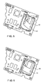
- FIG. 1 shows an exemplary embodiment of a circuit assembly according to the present invention
- FIG. 2 a shows a top view of an exemplary embodiment of a card mounting bracket according to the present invention
- FIG. 2 b shows a side view of an exemplary embodiment of a card mounting bracket according to the present invention
- FIG. 2 c shows a rear view of an exemplary embodiment of a card mounting bracket according to the present invention
- FIG. 3 shows a schematic view of a card mounting bracket and a printed circuit board according to the present invention
- FIG. 4 shows a schematic view of a card mounting bracket and a printed circuit board according to the present invention
- FIG. 5 shows a schematic view of a radio card, a card mounting bracket and a printed circuit board according to the present invention
- FIG. 6 shows a schematic view of a radio card, a card mounting bracket and a printed circuit board according to the present invention
- FIG. 7 shows a close-up view of a retaining member on a card mounting bracket and a radio card according to the present invention
- FIG. 8 shows a schematic view of a radio card and a card mounting bracket mounted to a printed circuit board according to the present invention
- FIG. 9 shows a schematic view of a card mounting bracket and a printed circuit board mounted to a reverse side thereof according to the present invention.
- FIG. 10 shows a schematic view of a card mounting bracket and a printed circuit board mounted to a reverse side thereof according to the present invention.
- FIG. 11 shows a schematic view of a radio card, a card mounting bracket and a printed circuit board mounted to a reverse side thereof according to the present invention
- the present invention may be further understood with reference to the following description and the appended drawings, wherein like elements are provided with the same reference numerals.
- the present invention describes a card holder arrangement for mounting an external component to a printed circuit board (“PCB”).
- PCB printed circuit board
- the exemplary embodiment will be described with reference to a PCB utilized in a wireless computing device, those of skill in the art will understand that the card holder arrangement of the present invention is scalable for use with larger/smaller external components (e.g., memory chips, standard PCI cards, etc.) and in larger/smaller computing devices (e.g., PCs, laptops, etc.).
- FIG. 1 shows an exemplary embodiment of a circuit assembly 10 according to the present invention.
- the assembly 10 according to this embodiment is utilized in a wireless computing device such as, for example, an image/laser-based scanner, an RFID reader/tag, a laptop, a phone, a PDA, a tablet, a network interface card, etc.
- the assembly 10 may be utilized in a stationary computing device such as a PC. That is, any computing device may utilize the assembly 10 for coupling an external component to a circuit board providing additional functionality to the computing device.
- the assembly 10 includes a printed circuit board (“PCB”) 12 , an external component (e.g., a radio card 14 ) and a component mounting bracket 16 .
- the PCB 12 may be any size, shape and/or design (e.g., form factor) known to those of skill in the art.
- the PCB 12 may include any number and variety of electrical components (e.g., processors, memory, etc.) coupled to either surface of the PCB 12 (e.g., top and/or bottom).
- the PCB 12 includes a card connector 18 for sustaining an electrical connection with the radio card 14 .
- the card connector 18 includes pins which, when in contact with pins of the radio card 14 , allow for an exchange of electrical signals between the radio card 14 and electrical components on the PCB 12 .
- At least one pair of slots 20 are formed adjacent to the card connector 18 allowing the bracket 16 to be mounted to the PCB 12 .
- the PCB 12 includes two pairs of slots 20 which allow two component mounting brackets 16 to be mounted thereto.
- two radio cards 14 may be mounted to substantially similar areas of the PCB 12 , on opposite sides thereof.
- the pairs of slots 20 may be formed in any suitable areas on the PCB 12 for mounting the brackets 16 and corresponding radio cards 14 thereto (e.g., on both sides of the PCB 12 ).
- a number of the pairs of slots 20 preferably correspond to a number of radio cards 14 to be mounted to the PCB 12 .
- the bracket 16 is preferably a frame formed of a single piece of material (e.g., plastic, rubber, ceramic, sheet metal, etc.) which is mountable to the PCB 12 without requiring mechanical and/or chemical fasteners.
- the bracket 16 may be manufactured using any conventional process (e.g., injection molding).
- Conventional radio card mounting brackets are generally mechanically fastened to the PCB 12 .
- the bracket 16 according to the present invention allows for toolless assembly of the bracket 16 to the PCB 12 and of the radio card 14 to the bracket 16 .
- the bracket 16 is interlocked to the PCB 12 using the slots 20 . After the bracket 16 is mounted to the PCB 12 , the radio card 14 is coupled to the card connector 18 and secured within the bracket 16 .
- the bracket 16 prevents the radio card 14 from coming loose from the card connector 18 thereby maintaining its electrical connection with the PCB 12 .
- the bracket 16 includes a front wall 22 , a rear wall 24 and sidewalls 26 , 28 enclosing a generally rectangular area 30 sized and shaped to complement the radio card 14 .
- the arrangement 10 may be of any size and/shape complementary to the size/shape of a component to be retained therein.
- a stack height of the bracket 16 is preferably similar to a stack height of the component secured thereby (e.g., the radio card 14 ).
- the bracket 16 prevents lateral and vertical displacement of the radio card 14 , as will be described further below.
- the sidewalls 26 , 28 are designed with a bow shape allowing a tension-extension length therein. The tension-extension length permits the rear wall 24 to move away from the front wall 22 for accommodating slight variances in the length of the radio card 14 which may ensure a snug fit at assembly.
- An inner face of the rear wall 24 includes ledges 30 , 32 which preferably have a stack height similar to that of as the card connector 18 . That is, when the radio card 14 is coupled to the card connector 18 , there is preferably a space between the radio card 14 and the surface of the PCB 12 . The radio card 14 rests on the ledges 30 , 32 to be maintained at the stack height of the card connector 18 providing integrity to the electrical connection.
- the bracket 16 may include a single ledge or a plurality of ledges for maintaining the radio card 14 at the stack height of the card connector 18 .
- the inner face of the rear wall 22 further includes a retaining member 34 centered between the ledges 30 , 32 at a predetermined height thereabove.
- the height is preferably equal to at least a thickness of the installed radio card 14 .
- the retaining member 34 preferably includes a protruding downward slope providing resistance to the radio card 14 as it is pushed onto the ledges 30 , 32 .
- the radio card 14 snap-fits between the slope and the ledges 30 , 32 .
- the retaining member 34 and the ledges 30 , 32 prevent the radio card 14 from moving vertically when coupled to the card connector 18 .
- each of the sidewalls 26 , 28 includes a notch 36 at a front end thereof and an interlocking tab 38 at a rear end thereof.
- the notch 36 provides space for a tab of a further bracket to be mounted on a substantially similar portion of the PCB 12 , but on an opposite side thereof.
- the tab 38 includes a foot 40 which retains the tab 38 within the slot 20 . That is, to lock the bracket 16 to the PCB 12 , the foot 40 is inserted into a portion of the slot 20 which is narrower than a width of the foot 40 . Thus, the bracket 16 cannot be removed from the PCB 12 until the foot 40 is removed from the slot 20 .
- the radio card 14 is removed from the bracket 16 by applying a compressive force to the sidewalls 26 , 28 . That is, the sidewalls 26 , 28 bow outward providing a predetermined clearance between themselves and the radio card 14 .
- the compressive force distends the rear wall 24 releasing the radio card 14 from the retaining member 34 .
- the radio card 14 may then be lifted from the bracket 16 .
- a cut-out 40 is provided in the rear wall 24 to facilitate lifting the radio card 14 from the bracket 16 .
- FIGS. 3-8 show an exemplary method of mounting the bracket 16 to the PCB 12 , coupling the radio card 14 to the card connector 18 and securing the radio card 14 in the bracket 16 .
- the tabs 38 are inserted into the slots 20 .
- a wide portion of the slot 20 receives the foot 40 while a narrow portion of the slot 20 retains the foot 40 securing the bracket to the PCB 12 .
- FIG. 4 the bracket 16 is mounted to the PCB 12 with the tabs 38 interlocked with the slots 20 and the front wall 22 abutting the card connector 18 .
- FIG. 5 shows the radio card 14 being coupled to the card connector 18 with the electrical contacts of the radio card 14 contacting corresponding contacts on the card connector 18 .
- FIG. 6 the radio card 14 is shown with the electrical contacts thereof fully engaged with the contacts of the PCB 12 and the card connector 18 with a first side of the radio card 14 contacting the bracket 16 .
- the radio card 14 has not yet been inserted between the retaining member 34 and the ledges 30 , 32 .
- FIG. 7 shows the radio card 14 after it has been pushed past the retaining member 34 to secure the radio card 14 within the bracket 16 and prevent vertical displacement of the radio card 14 during use, a shock event, etc.
- FIG. 8 shows a complete mechanical and electrical assembly of the PCB 12 , bracket 16 and radio card 14 .
- the bracket 16 is preferably sized to fence-in the radio card 14 and the card connector 18 .
- the bracket 16 is prevented from disengaging the slots 20 , because the radio card 14 prevents movement of the rear wall 24 .
- the tabs 38 cannot reach the portion of the slots 20 from which the foot 40 may exit.
- FIG. 8 also shows that when installed, electrical components on the radio card 14 are exposed.
- This configuration allows external heat-sinking of hot areas the radio card 14 improving performance and life.
- a conventional heat sink may be placed adjacent the exposed area of the radio card 14 .
- the bracket 16 may be fitted with a cover (not shown) over the area 30 which would aid in electromagnetic shielding and electrostatic discharge protection.
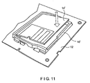
- a further radio card 14 ′ may be mounted on an opposite side of the PCB 12 as shown in FIGS. 9-11 .
- a bracket 16 ′ is interlocked with slots 20 ′ in a manner substantially similar to that described above in regard to the bracket 16 and the slots 20 .
- a notch 36 ′ in the bracket 16 ′ provides clearance for the tab 38 of the bracket 16 mounted on the opposite side of the PCB 12 .
- multiple radio cards may be stacked on the PCB 12 .
- the further radio card 14 ′ is mounted to and removed from the bracket 16 ′ in the manner described above.
- the disclosed exemplary embodiments of the present invention may withstand approximately 0.02 g 2 /Hz of random vibration in all three axises, approximately 20 Hz to 2000 Hz.
- the exemplary embodiments may also withstand at least a ninety-one (91) centimeter drop to a hard surface (e.g., concrete).
Abstract
Description
Claims (18)
Priority Applications (1)
| Application Number | Priority Date | Filing Date | Title |
|---|---|---|---|
| US11/265,715 US7623357B2 (en) | 2005-11-02 | 2005-11-02 | Card holder arrangement for circuit assembly |
Applications Claiming Priority (1)
| Application Number | Priority Date | Filing Date | Title |
|---|---|---|---|
| US11/265,715 US7623357B2 (en) | 2005-11-02 | 2005-11-02 | Card holder arrangement for circuit assembly |
Publications (2)
| Publication Number | Publication Date |
|---|---|
| US20070097663A1 US20070097663A1 (en) | 2007-05-03 |
| US7623357B2 true US7623357B2 (en) | 2009-11-24 |
Family
ID=37996020
Family Applications (1)
| Application Number | Title | Priority Date | Filing Date |
|---|---|---|---|
| US11/265,715 Active 2026-11-24 US7623357B2 (en) | 2005-11-02 | 2005-11-02 | Card holder arrangement for circuit assembly |
Country Status (1)
| Country | Link |
|---|---|
| US (1) | US7623357B2 (en) |
Cited By (4)
| Publication number | Priority date | Publication date | Assignee | Title |
|---|---|---|---|---|
| US20100053917A1 (en) * | 2008-08-28 | 2010-03-04 | Chi Mei Communication Systems, Inc. | Chip card holder |
| US20110171846A1 (en) * | 2010-01-11 | 2011-07-14 | Dell Products L.P. | Circuit Card Latching Arm Arresting Apparatus |
| US9740249B2 (en) | 2014-01-30 | 2017-08-22 | Hewlett Packard Enterprise Development Lp | Mounting device |
| US10416728B2 (en) | 2015-02-20 | 2019-09-17 | Hewlett Packard Enterprise Development Lp | Tool-less multipoint latching mechanism |
Citations (22)
| Publication number | Priority date | Publication date | Assignee | Title |
|---|---|---|---|---|
| US4774126A (en) * | 1987-07-20 | 1988-09-27 | General Electric Company | Solderable thermoplastic structure |
| US5267973A (en) * | 1991-04-08 | 1993-12-07 | Habley Medical Technology Corporation | Safety syringe with off-axis needle cannula |
| US5333100A (en) * | 1992-06-29 | 1994-07-26 | Itt Corporation | Data card perimeter shield |
| US5337220A (en) * | 1993-09-10 | 1994-08-09 | The Whitaker Corporation | Electronic card and connector assembly for use therewith |
| US5373149A (en) * | 1993-02-01 | 1994-12-13 | At&T Bell Laboratories | Folding electronic card assembly |
| US5490038A (en) * | 1994-04-06 | 1996-02-06 | Dell Usa, L.P. | Adapter apparatus for use in connecting a printed circuit board to a computer chasis |
| US6075706A (en) * | 1998-04-07 | 2000-06-13 | Itt Manufacturing Enterprises, Inc. | PC card for receiving chip card |
| US6104620A (en) * | 1993-12-23 | 2000-08-15 | Symbol Technologies, Inc. | Shielded radio card assembly |
| US6231364B1 (en) * | 1997-07-19 | 2001-05-15 | Chao-Zen Liu | Memory module connector |
| US6234821B1 (en) * | 1999-09-29 | 2001-05-22 | Ying Wu Tan | Connector for ram module |
| US6270369B1 (en) * | 1999-04-15 | 2001-08-07 | International Business Machines Corporation | Sub-card board connector, sub-card board, modem sub-card, and a computer having this connector |
| US6286638B1 (en) * | 2000-07-20 | 2001-09-11 | International Truck And Engine Corporation | Anti-lock brake sensor bracket |
| US6394831B1 (en) * | 1999-08-06 | 2002-05-28 | The Whitaker Corporation | Retention member for card edge connector |
| US6517369B1 (en) * | 2002-03-14 | 2003-02-11 | International Business Machines Corporation | Retention bracket/collar for circuit cards |
| US6589259B1 (en) * | 1999-12-28 | 2003-07-08 | Karl Storz Gmbh & Co. Kg | Medical instrument, particularly a surgical instrument |
| US6731517B1 (en) * | 2003-03-12 | 2004-05-04 | Hon Hai Precision Ind. Co., Ltd. | Card edge connector with metal springs |
| US6971899B1 (en) * | 2004-05-14 | 2005-12-06 | Chin-Ching Liu | Fastening device for card |
| US7014492B1 (en) * | 2004-11-30 | 2006-03-21 | Symbol Technologies, Inc. | Wireless circuit assembly and apparatus for securing card edge connectors therein |
| US7049172B2 (en) * | 2004-02-06 | 2006-05-23 | 3 View Technology Co., Ltd. | Packaging structure and process of electronic card |
| US7077678B1 (en) * | 2005-01-18 | 2006-07-18 | Hon Hai Precision Ind. Co., Ltd. | Electrical connector assembly having board hold down |
| US7211743B1 (en) * | 2005-12-14 | 2007-05-01 | General Instrument Corporation | Apparatus for supporting printed wiring assemblies in a device housing |
| US7354290B2 (en) * | 2006-03-23 | 2008-04-08 | Shenzhen Futaihong Precision Industry Co., Ltd. | Surface contact card holder |
-
2005
- 2005-11-02 US US11/265,715 patent/US7623357B2/en active Active
Patent Citations (22)
| Publication number | Priority date | Publication date | Assignee | Title |
|---|---|---|---|---|
| US4774126A (en) * | 1987-07-20 | 1988-09-27 | General Electric Company | Solderable thermoplastic structure |
| US5267973A (en) * | 1991-04-08 | 1993-12-07 | Habley Medical Technology Corporation | Safety syringe with off-axis needle cannula |
| US5333100A (en) * | 1992-06-29 | 1994-07-26 | Itt Corporation | Data card perimeter shield |
| US5373149A (en) * | 1993-02-01 | 1994-12-13 | At&T Bell Laboratories | Folding electronic card assembly |
| US5337220A (en) * | 1993-09-10 | 1994-08-09 | The Whitaker Corporation | Electronic card and connector assembly for use therewith |
| US6104620A (en) * | 1993-12-23 | 2000-08-15 | Symbol Technologies, Inc. | Shielded radio card assembly |
| US5490038A (en) * | 1994-04-06 | 1996-02-06 | Dell Usa, L.P. | Adapter apparatus for use in connecting a printed circuit board to a computer chasis |
| US6231364B1 (en) * | 1997-07-19 | 2001-05-15 | Chao-Zen Liu | Memory module connector |
| US6075706A (en) * | 1998-04-07 | 2000-06-13 | Itt Manufacturing Enterprises, Inc. | PC card for receiving chip card |
| US6270369B1 (en) * | 1999-04-15 | 2001-08-07 | International Business Machines Corporation | Sub-card board connector, sub-card board, modem sub-card, and a computer having this connector |
| US6394831B1 (en) * | 1999-08-06 | 2002-05-28 | The Whitaker Corporation | Retention member for card edge connector |
| US6234821B1 (en) * | 1999-09-29 | 2001-05-22 | Ying Wu Tan | Connector for ram module |
| US6589259B1 (en) * | 1999-12-28 | 2003-07-08 | Karl Storz Gmbh & Co. Kg | Medical instrument, particularly a surgical instrument |
| US6286638B1 (en) * | 2000-07-20 | 2001-09-11 | International Truck And Engine Corporation | Anti-lock brake sensor bracket |
| US6517369B1 (en) * | 2002-03-14 | 2003-02-11 | International Business Machines Corporation | Retention bracket/collar for circuit cards |
| US6731517B1 (en) * | 2003-03-12 | 2004-05-04 | Hon Hai Precision Ind. Co., Ltd. | Card edge connector with metal springs |
| US7049172B2 (en) * | 2004-02-06 | 2006-05-23 | 3 View Technology Co., Ltd. | Packaging structure and process of electronic card |
| US6971899B1 (en) * | 2004-05-14 | 2005-12-06 | Chin-Ching Liu | Fastening device for card |
| US7014492B1 (en) * | 2004-11-30 | 2006-03-21 | Symbol Technologies, Inc. | Wireless circuit assembly and apparatus for securing card edge connectors therein |
| US7077678B1 (en) * | 2005-01-18 | 2006-07-18 | Hon Hai Precision Ind. Co., Ltd. | Electrical connector assembly having board hold down |
| US7211743B1 (en) * | 2005-12-14 | 2007-05-01 | General Instrument Corporation | Apparatus for supporting printed wiring assemblies in a device housing |
| US7354290B2 (en) * | 2006-03-23 | 2008-04-08 | Shenzhen Futaihong Precision Industry Co., Ltd. | Surface contact card holder |
Cited By (5)
| Publication number | Priority date | Publication date | Assignee | Title |
|---|---|---|---|---|
| US20100053917A1 (en) * | 2008-08-28 | 2010-03-04 | Chi Mei Communication Systems, Inc. | Chip card holder |
| US8059419B2 (en) * | 2008-08-28 | 2011-11-15 | Chi Mei Communication Systems, Inc. | Chip card holder |
| US20110171846A1 (en) * | 2010-01-11 | 2011-07-14 | Dell Products L.P. | Circuit Card Latching Arm Arresting Apparatus |
| US9740249B2 (en) | 2014-01-30 | 2017-08-22 | Hewlett Packard Enterprise Development Lp | Mounting device |
| US10416728B2 (en) | 2015-02-20 | 2019-09-17 | Hewlett Packard Enterprise Development Lp | Tool-less multipoint latching mechanism |
Also Published As
| Publication number | Publication date |
|---|---|
| US20070097663A1 (en) | 2007-05-03 |
Similar Documents
| Publication | Publication Date | Title |
|---|---|---|
| JP7305760B2 (en) | Card connectors, card holders and terminal devices | |
| US7789691B2 (en) | Chip card retaining mechanism and printed circuit board module incorporating same | |
| US8238097B2 (en) | Computer system | |
| US20110079701A1 (en) | Connection Device | |
| US7623357B2 (en) | Card holder arrangement for circuit assembly | |
| JPH08236215A (en) | Universal ground clip for card acceptance connector | |
| US7651357B2 (en) | IC socket | |
| US7922523B2 (en) | Vertically stackable sockets for chip modules | |
| US7701651B2 (en) | Lens module structure with a metal shell and assembling method therefor | |
| US7445506B2 (en) | Shielded connector | |
| US5463531A (en) | PCMCIA electronics housing | |
| US20110151721A1 (en) | Electrical card connector | |
| US8254130B2 (en) | Computer system | |
| US7626826B2 (en) | Expansion card carrier and method for assembling the same | |
| US20130033832A1 (en) | Mounting apparatus for pci card | |
| US7252528B1 (en) | Mounting assembly for expansion card | |
| JP2003124655A (en) | Circuit substrate | |
| US6768644B2 (en) | Compact flash card | |
| US8456848B2 (en) | Computer enclosure having expansion card retention frame | |
| JP6960996B2 (en) | Electronic device | |
| JP7220384B2 (en) | Battery holder and wireless device | |
| US20090190300A1 (en) | Parts support apparatus | |
| CN108736190B (en) | Dual connector system | |
| EP1291805B1 (en) | Connector for memory card | |
| US20070093138A1 (en) | Electronic card connection devices |
Legal Events
| Date | Code | Title | Description |
|---|---|---|---|
| AS | Assignment |
Owner name: SYMBOL TECHNOLOGIES, INC., NEW YORK Free format text: ASSIGNMENT OF ASSIGNORS INTEREST;ASSIGNOR:WALLACE, PATRICK;REEL/FRAME:017189/0494 Effective date: 20051101 |
|
| STCF | Information on status: patent grant |
Free format text: PATENTED CASE |
|
| CC | Certificate of correction | ||
| FPAY | Fee payment |
Year of fee payment: 4 |
|
| AS | Assignment |
Owner name: MORGAN STANLEY SENIOR FUNDING, INC. AS THE COLLATERAL AGENT, MARYLAND Free format text: SECURITY AGREEMENT;ASSIGNORS:ZIH CORP.;LASER BAND, LLC;ZEBRA ENTERPRISE SOLUTIONS CORP.;AND OTHERS;REEL/FRAME:034114/0270 Effective date: 20141027 Owner name: MORGAN STANLEY SENIOR FUNDING, INC. AS THE COLLATE Free format text: SECURITY AGREEMENT;ASSIGNORS:ZIH CORP.;LASER BAND, LLC;ZEBRA ENTERPRISE SOLUTIONS CORP.;AND OTHERS;REEL/FRAME:034114/0270 Effective date: 20141027 |
|
| AS | Assignment |
Owner name: SYMBOL TECHNOLOGIES, LLC, NEW YORK Free format text: CHANGE OF NAME;ASSIGNOR:SYMBOL TECHNOLOGIES, INC.;REEL/FRAME:036083/0640 Effective date: 20150410 |
|
| AS | Assignment |
Owner name: SYMBOL TECHNOLOGIES, INC., NEW YORK Free format text: RELEASE BY SECURED PARTY;ASSIGNOR:MORGAN STANLEY SENIOR FUNDING, INC.;REEL/FRAME:036371/0738 Effective date: 20150721 |
|
| FPAY | Fee payment |
Year of fee payment: 8 |
|
| MAFP | Maintenance fee payment |
Free format text: PAYMENT OF MAINTENANCE FEE, 12TH YEAR, LARGE ENTITY (ORIGINAL EVENT CODE: M1553); ENTITY STATUS OF PATENT OWNER: LARGE ENTITY Year of fee payment: 12 |