US7638951B2 - Plasma lamp with stable feedback amplification and method therefor - Google Patents
Plasma lamp with stable feedback amplification and method therefor Download PDFInfo
- Publication number
- US7638951B2 US7638951B2 US11/553,881 US55388106A US7638951B2 US 7638951 B2 US7638951 B2 US 7638951B2 US 55388106 A US55388106 A US 55388106A US 7638951 B2 US7638951 B2 US 7638951B2
- Authority
- US
- United States
- Prior art keywords
- amplifier
- lamp
- phase
- load trajectory
- unstable region
- Prior art date
- Legal status (The legal status is an assumption and is not a legal conclusion. Google has not performed a legal analysis and makes no representation as to the accuracy of the status listed.)
- Expired - Fee Related, expires
Links
Images


Classifications
-
- H—ELECTRICITY
- H05—ELECTRIC TECHNIQUES NOT OTHERWISE PROVIDED FOR
- H05B—ELECTRIC HEATING; ELECTRIC LIGHT SOURCES NOT OTHERWISE PROVIDED FOR; CIRCUIT ARRANGEMENTS FOR ELECTRIC LIGHT SOURCES, IN GENERAL
- H05B41/00—Circuit arrangements or apparatus for igniting or operating discharge lamps
- H05B41/14—Circuit arrangements
- H05B41/26—Circuit arrangements in which the lamp is fed by power derived from dc by means of a converter, e.g. by high-voltage dc
- H05B41/28—Circuit arrangements in which the lamp is fed by power derived from dc by means of a converter, e.g. by high-voltage dc using static converters
- H05B41/2806—Circuit arrangements in which the lamp is fed by power derived from dc by means of a converter, e.g. by high-voltage dc using static converters with semiconductor devices and specially adapted for lamps without electrodes in the vessel, e.g. surface discharge lamps, electrodeless discharge lamps
-
- H—ELECTRICITY
- H01—ELECTRIC ELEMENTS
- H01J—ELECTRIC DISCHARGE TUBES OR DISCHARGE LAMPS
- H01J65/00—Lamps without any electrode inside the vessel; Lamps with at least one main electrode outside the vessel
- H01J65/04—Lamps in which a gas filling is excited to luminesce by an external electromagnetic field or by external corpuscular radiation, e.g. for indicating plasma display panels
- H01J65/042—Lamps in which a gas filling is excited to luminesce by an external electromagnetic field or by external corpuscular radiation, e.g. for indicating plasma display panels by an external electromagnetic field
- H01J65/044—Lamps in which a gas filling is excited to luminesce by an external electromagnetic field or by external corpuscular radiation, e.g. for indicating plasma display panels by an external electromagnetic field the field being produced by a separate microwave unit
-
- H—ELECTRICITY
- H05—ELECTRIC TECHNIQUES NOT OTHERWISE PROVIDED FOR
- H05B—ELECTRIC HEATING; ELECTRIC LIGHT SOURCES NOT OTHERWISE PROVIDED FOR; CIRCUIT ARRANGEMENTS FOR ELECTRIC LIGHT SOURCES, IN GENERAL
- H05B41/00—Circuit arrangements or apparatus for igniting or operating discharge lamps
- H05B41/14—Circuit arrangements
- H05B41/24—Circuit arrangements in which the lamp is fed by high frequency ac, or with separate oscillator frequency
-
- Y—GENERAL TAGGING OF NEW TECHNOLOGICAL DEVELOPMENTS; GENERAL TAGGING OF CROSS-SECTIONAL TECHNOLOGIES SPANNING OVER SEVERAL SECTIONS OF THE IPC; TECHNICAL SUBJECTS COVERED BY FORMER USPC CROSS-REFERENCE ART COLLECTIONS [XRACs] AND DIGESTS
- Y02—TECHNOLOGIES OR APPLICATIONS FOR MITIGATION OR ADAPTATION AGAINST CLIMATE CHANGE
- Y02B—CLIMATE CHANGE MITIGATION TECHNOLOGIES RELATED TO BUILDINGS, e.g. HOUSING, HOUSE APPLIANCES OR RELATED END-USER APPLICATIONS
- Y02B20/00—Energy efficient lighting technologies, e.g. halogen lamps or gas discharge lamps
Definitions
- the field of the present invention relates to systems and methods for generating light, and more particularly to electrodeless plasma lamps.
- Electrodeless plasma lamps may be used to provide point-like, bright, white light sources. Because electrodes are not used, they may have longer useful lifetimes than other lamps. Some plasma lamps direct microwave energy into an air cavity, with the air cavity enclosing a bulb containing a mixture of substances that can ignite, form a plasma, and emit light. However, for many applications, light sources that are brighter, smaller, less expensive, more reliable, and have longer useful lifetimes are desired.
- Some plasma lamps use a solid dielectric waveguide body.
- An amplifier may be used to provide power to the waveguide body at a frequency causing it to resonate.
- a positive-feedback loop may be used to maintain resonance during operation of the lamp. Feedback obviates the need for precise prediction and implementation of the resonant frequency, enabling manufacturing tolerances on the body to be relaxed. Moreover, feedback maintains coupling across resonant frequency changes associated with large temperature swings. Instead of requiring a precisely tuned microwave source at a predicted, preselected operating frequency, an amplifier with a feedback loop can be used to adjust to changing lamp conditions during operation.
- What is desired are improved systems and methods for providing power to, and obtaining feedback from, a plasma lamp to maintain a resonant condition. What is also desired are systems and methods for stable operation of a plasma lamp using amplifiers that have unstable regions of operation.
- An example embodiment provides a plasma lamp including a waveguide body of dielectric material having a dielectric constant greater than about 2, a plasma bulb adjacent to the body, first and second probes positioned within the body, and an amplifier coupled to the first and second probes.
- the amplifier includes an unstable region of operation. A phase exists where the load trajectory would cross the unstable region of the amplifier.
- the lamp further includes means for ensuring amplifier stability under all operating conditions.
- the transmission lines may be selected to provide for stable operation or phase shifting may be used to provide for stable operation.
- the lamp may include means for critically coupling the amplifier to the first probe after the plasma reaches steady state.
- phase shifting may be used to critically couple the amplifier to the first probe after the plasma reaches steady state.
- a method of generating light is provided.
- a lamp body and a bulb have a load trajectory from start-up to steady state operation.
- Power is coupled to the lamp body from an amplifier using feedback from the lamp body.
- a phase exists such that the load trajectory would cross the unstable region of operation.
- the phase of the feedback is adjusted such that the load trajectory does not cross the unstable region of the amplifier.
- a method for configuring a plasma lamp, powered by an amplifier, with a positive-loop feedback topology such that the amplifier remains stable and the loop resonant for all operating conditions.
- the method may include, for all load conditions, measuring at an amplifier input the magnitude and phase of the outgoing and reflected electric fields; for each load condition, determining a load trajectory by plotting the field-ratio on a complex plane; identifying regions on the complex plane where the amplifier is stable and unstable; and overlaying the regions on the load trajectory to predict circuit behavior.
- the circuit design may then be selected to operate within the stable regions by selecting transmission lines that will cause operation in the stable regions or by using phase shifting to operate the lamp in the stable regions.
- FIG. 1 schematically depicts a cross-sectional view of a plasma lamp using an amplifier with an unstable region of operation according to an example embodiment.
- FIG. 2 schematically depicts a positive-feedback loop broken at the amplifier input.
- FIG. 3A schematically depicts ⁇ , the reflection coefficient.
- FIG. 3B illustrates a load trajectory polar-plot where ⁇ changes in phase but not in magnitude.
- FIG. 3C illustrates a load trajectory polar-plot where ⁇ changes in magnitude but not in phase.
- FIG. 4A is a load trajectory polar-plot for an amplifier that is stable over the entire load trajectory of a lamp for any phase.
- FIG. 4B depicts a load trajectory polar-chart for an example amplifier which has stable and unstable regions of operation.
- FIG. 5A schematically depicts an example plasma lamp circuit using an amplifier in an unstable configuration.
- FIG. 5B schematically depicts the FIG. 5A lamp circuit with the cable connecting the amplifier output and drive probe altered in length to provide for stable operation of the amplifier.
- FIG. 5C is a polar-chart overlaying the regions of stability and instability on the load trajectories of the FIGS. 5A and 5B lamp circuits.
- FIG. 6A schematically depicts an example plasma lamp circuit using an amplifier in an unstable configuration.
- FIG. 6B schematically depicts the FIG. 6A lamp circuit modified by inserting a phase-shifter between the amplifier output and drive probe to provide for stable operation of the amplifier.
- FIG. 6C schematically depicts the FIG. 6A lamp circuit modified by inserting a phase-shifter and an attenuator between the amplifier output and drive probe to provide for stable operation of the amplifier.
- FIG. 6D is a polar-chart overlaying regions of stability and instability on the load trajectories of the FIGS. 6A , 6 B and 6 C lamp circuits.
- FIG. 7A schematically depicts an example plasma lamp having a cylindrical waveguide body and a drive probe, feedback probe, and start probe.
- the feedback probe is connected to the drive probe by an amplifier and a splitter, and connected to the start probe by the amplifier, splitter, and a phase-shifter.
- FIG. 7B schematically depicts an example plasma lamp having a cylindrical body and a drive probe, feedback probe, and start probe.
- the feedback probe is connected to the drive probe and start probe by an amplifier and a circulator.
- FIG. 8A schematically depicts an example plasma lamp having a cylindrical body and a drive probe and feedback probe connected by an amplifier.
- a start resonant mode is used before plasma formation, and a drive resonant mode is used to power the plasma to steady state.
- FIG. 8B schematically depicts an example plasma lamp having a cylindrical body and a drive probe and feedback probe connected by first and second amplifiers and first and second diplexers.
- FIG. 9A schematically depicts an example plasma lamp having a cylindrical body and a drive probe, feedback probe, and start probe.
- the feedback probe is connected to the drive probe and start probe by an amplifier and a diplexer.
- FIG. 9B schematically depicts an example plasma lamp having a cylindrical body and a drive probe, feedback probe, and start probe.
- the feedback probe is connected to the drive probe by a diplexer and a first amplifier, and to the start probe by the diplexer and a second amplifier.
- FIG. 10A is a side view of a lamp according to an example embodiment with a connector to a drive probe and a connector to a feedback probe according to an example embodiment.
- FIG. 10B is a chart illustrating coupling between a port for a drive probe and a port for a feedback probe for the lamp of FIG. 10A as a function of frequency during periods of lamp operation from ignition to steady state.
- FIG. 10C is a flow chart of a method for operating a lamp according to an example embodiment.
- FIG. 10D is a flow chart of a method for brightness adjustment according to an example embodiment.
- an example embodiment provides a plasma lamp 20 with a waveguide body 22 comprising a dielectric material.
- the waveguide body 22 may have a dielectric constant greater than 2.
- the body 22 may be solid and comprise alumina or other dielectric material.
- a power source such as an amplifier 24 , may be coupled to the waveguide body 22 to provide power to the waveguide at a frequency in the range of 50 MHz to 30 GHz or any range subsumed therein.
- the amplifier 24 may be coupled to a drive probe 26 to provide power to the waveguide body 22 .
- the drive probe 26 may be inserted into an opening formed in the waveguide body and may be in direct contact with the waveguide body 22 to effectively couple power into the waveguide body.
- a feedback probe 28 may be coupled to the waveguide body 22 and the amplifier 24 to obtain feedback from the waveguide body 22 and provide it to the amplifier 24 .
- the feedback probe 28 may be inserted into an opening formed in the waveguide body 22 and may be in direct contact with the waveguide body 22 to effectively obtain feedback from the waveguide body 22 .
- a bulb 25 may be positioned to receive power from the waveguide body 22 .
- the bulb 25 may contain a gas-fill that forms a plasma and emits light when power is provided from the waveguide body 22 to the bulb 25 .
- the bulb 25 may be positioned in an opening formed in the waveguide body 22 .
- the waveguide body 22 is configured to resonate when power is provided by the amplifier 24 to the drive probe 26 at a particular frequency.
- the ignition of the plasma in the bulb 25 and heating of the bulb 25 and the waveguide body 22 may cause resonant conditions to change (for example, due to changes in the load characteristics and thermal expansion of the bulb 25 and waveguide body 22 ).
- the feedback adjusts to changing lamp conditions to sustain oscillation.
- the amplifier 24 is unstable in regions of its operation.
- An unstable amplifier may have higher performance than an amplifier that is stable throughout the full range of operating conditions and load trajectories that can be used by the lamp. While it may be desirable to use amplifiers with some unstable regions, this may cause failure during operation and, in some cases, may cause the amplifier to explode.
- the load characteristics of the lamp 20 may change during operation due to ignition of the plasma, thermal expansion and adjustments to the feedback loop. As a result, the amplifier 24 is required to operate across a range of operating conditions and may fail if the operating conditions fall within an unstable region of the amplifier 24 . Accordingly, example embodiments provide systems and methods for using amplifiers with unstable regions of operation, while providing for stable operation of an electrodeless plasma lamp.
- the plasma lamp 20 of FIG. 1 is an example only and other lamp embodiments may also be utilized, such as those disclosed in co-pending U.S. applications: provisional application Ser. No. 60/730,654, titled “Plasma Lamp Using a Shaped Waveguide Body”; provisional application Ser. No. 60/730,785, titled “Plasma Lamp and Methods Using a Waveguide Body and Protruding Bulb” filed Oct. 27, 2005; provisional application Ser. No. 60/730,950, titled “Plasma Lamp with Compact Waveguide” filed Oct. 27, 2005; provisional application Ser. No. 60/730,953, titled “High Brightness Plasma Lamp” filed Oct. 27, 2005; and provisional application Ser. No. 60/730,786, titled “Plasma Lamp with Phase Control” filed Oct. 27, 2005, each of which is incorporated herein by reference in its entirety.
- the topology of FIG. 1 is a positive-feedback loop.
- Positive feedback loops can be used to sustain oscillations at frequencies satisfying two basic conditions. First, the loop's gain, provided by an amplifier, is greater than the total loss in the loop. Secondly, the total phase shift of an electromagnetic wave traversing the loop is such that the wave reproduces itself, and thus, undergoes some N-multiple of 2 ⁇ in phase change, so as to constructively form a stationary wave. This concept is illustrated in FIG. 2 which shows the “open-loop” system associated with the “closed-loop” system of FIG. 1 .
- the “feedback loop” 30 F is “broken” at an arbitrary point, here amplifier input port 24 A.
- a complex multiplier S 21 takes a wave from Port- 1 to Port- 2 .
- S 21 typically varies as a function of frequency; at any given frequency, the required conditions for resonance are:
- >1; and angle (S 21 ) 2 ⁇ N. These two conditions select for a series of possible frequencies.
- the waveguide body behaves as a lossy narrow band-pass filter; any element in the loop having a band-pass spectral characteristic serves to select a single preferred frequency of oscillation.
- the cavity selects its resonant frequency to pass from the feedback probe to the drive probe. This signal is then amplified and delivered back into the cavity via the drive probe. Oscillation persists when the net phase shift of the total loop, consisting of feedback loop 30 F and “drive loop” 30 D, is such that a frequency preferred by the body is also one which constructively forms stationary waves in feedback loop 30 F.
- FIG. 3A illustrates the definition of a parameter ⁇ , the “reflection coefficient,” a measure of the changing load condition over the various phases of lamp operation, particularly the transition from cold gas at start-up to hot plasma at steady state.
- ⁇ defined with respect to a reference plane “RP” at the amplifier output, is the ratio of the “reflected” electric field E in heading into the amplifier, to the “outgoing” electric field E out traveling out. Being a ratio of fields, ⁇ is a complex number with a magnitude and phase.
- a useful way to depict changing conditions in a system is to use a “polar-chart” plot of ⁇ 's behavior (termed a “load trajectory”) on the complex plane.
- a polar-plot depicts ⁇ at a particular frequency.
- FIG. 3B if ⁇ changes in phase but not in magnitude the load trajectory(ies) will be circular. Circuit alterations leading to a circular load trajectory include altering the lengths (and therefore the phase of propagation) of one or both transmission lines (here, cables), and/or altering the reactance (capacitance and/or inductance) of circuit components. Such compensation may be useful for adjusting the starting angle of ⁇ .
- FIG. 3C if ⁇ changes in magnitude but not in phase the load trajectory(ies) will be radial.
- ⁇ may be used to determine amplifier stability.
- stability behavior “S”—stable for a ⁇ crossing that region on the polar-chart; and “U”—unstable so that for a ⁇ crossing that region, the amplifier exhibits failure conditions such oscillation and/or catastrophic failure.
- the stable region of some amplifiers depends upon the bias voltage applied to the amplifier.
- the regions that require a particular bias voltage in order to be stable are sometimes referred to as “conditionally stable.” In example embodiments, these regions are considered stable if the required bias voltage is applied, and unstable if the bias voltage is not applied.
- regions of S and U may first be identified on a polar-chart, overlaying them on the load trajectory to predict circuit behavior.
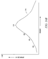
- FIG. 4A is a polar-plot for an amplifier that is stable over load trajectories LT 1 and LT 2 for any phase. This amplifier would be stable even if connected so that the load trajectories had a different phase. As a result, this amplifier is considered stable across the load trajectories LT 1 and LT 2 for a lamp, regardless of phase-shifting caused by the feedback circuit or transmission lines connecting the amplifier to the waveguide body.
- FIG. 4B is a polar-plot for an amplifier with limited regions of stability. Load trajectory LT 3 would result in acceptable system behavior, while load trajectory LT 4 (the same load trajectory at a different phase) would result in system failure.
- Example techniques for compensation to provide for stable lamp operation are disclosed herein. These example techniques allow amplifiers with unstable regions of operation to be used with a plasma lamp.
- the load trajectory and resonance condition may be independently tuned. This takes advantage of the fact that while ⁇ depends on the characteristics of transmission between the amplifier output and the load (lamp), loop resonance depends on the transmission of the entire loop.
- One example compensation technique is to choose the length L 1 of transmission line L 1 connecting the amplifier to the drive probe to tune the phase shift from the amplifier to the drive probe for operation in a stable region of the amplifier.
- the primary effect of adjusting L 1 in example embodiments is to rotate the starting point of the load trajectory along a circle of nearly constant radius on the ⁇ -plane.
- L 1 the primary effect of a lamp starting from a cold state with high reflectivity to a hot state with low reflectivity is to move radially inward on the ⁇ -plane, with relatively little phase change. Therefore, once the regions of amplifier stability are known, length L 1 can be adjusted to ensure that the ⁇ -trace passes only through those regions. This is illustrated by way of example in FIGS. 5A , 5 B and 5 C.
- the FIG. 5A system has a load trajectory LT 5 ( FIG. 5C ) causing amplifier instability as the lamp transitions from cold to hot.
- the compensation technique FIG.
- the load trajectory LT 6 is to change the length of connecting cable L 1 from L 1 to L 1 + ⁇ L 1 .
- the load trajectory is rotated to be well within the stable region.
- the amplifier will remain stable.
- the load trajectory LT 6 is at least 45° from any unstable region.
- the phase could shift by 45° and still remain within a stable region.
- the angular distance between the typical load trajectory for the lamp and the unstable region of the amplifier in either direction may be selected to be in the range of 5°-90°, or any range subsumed therein.
- the angular distance may be at least 15°, 30°, 45° or 60° in one direction from the load trajectory to the boundary of the unstable region and may be at least 15°, 30°, 45° or 60° in the other direction.
- the angular distance in one direction may not be the same as the angular distance in the other direction, and any combination of the above distances may be used in example embodiments.
- the angular distance in each direction for the load trajectory to the unstable region may be the same (essentially centering the load trajectory in the stable region) or be substantially the same (for example, ⁇ 5° or ⁇ 10° in one direction vis-à-vis the other).
- resonance conditions for the feedback loop are satisfied in the presence of phase shifts associated with tuning for amplifier stability.
- the technique is to first adjust length L 1 to satisfy amplifier stability, and then adjust the length L 2 of transmission line L 2 such that the total loop phase shift is a multiple of 2 ⁇ .
- the latter step may be performed by trial and error until good loop resonance is achieved.
- a second example compensation technique is to adjust the phase and/or magnitude using circuit elements.
- an adjustable phase-shifter is used between the amplifier and waveguide body.
- a phase-shifter is a passive LC-circuit that is reactive at frequencies of interest. This permits manual tuning of the loop phase.
- Another example embodiment is an “active” phase-shifter controlled by a controller such as a microprocessor, microcontroller or other control circuit.
- the controller may be external to the phase-shifter.
- the controller may be integrated with the phase-shifter. Active design permits optimization of the loop phase both at lamp start-up and after the lamp reaches steady state.
- the PS214-315 voltage-controlled phase-shifter commercially available from Skyworks Solutions, Inc. of Woburn, Mass. may be used in some embodiments.
- FIG. 6C An adjustable attenuator, when placed in series with the phase-shifter, permits simultaneous adjustment of the magnitude and phase of the load trajectory's starting point.
- FIG. 6C shows a phase-shifter 40 and attenuator 42 are connected between amplifier output port 24 B and drive probe 26 .
- the load trajectory LT 7 ( FIG. 6D ) of the FIG. 6A lamp circuit is almost entirely in the unstable region U.
- FIG. 6B shows the FIG. 6A lamp circuit modified by inserting a phase-shifter 44 between the amplifier output and drive probe. Phase-shifter 44 is used to rotate the starting point P 8 of ⁇ such that load trajectory LT 8 remains within the stable region S through lamp start-up.
- FIG. 6D depicts a scenario where phase-shifter 40 or 44 has been adjusted to match the phase shift caused by length ⁇ L 1 (see FIG. 5B ) so that the FIGS. 5C and 6D polar-charts match. This is an example only, and other approaches may also be used. Once phase-shifter 40 or 44 is adjusted for amplifier stability, length L 2 is adjusted for loop resonance.
- the feedback circuit may be adjusted to position the load trajectory within a stable region of operation for the amplifier.
- the position may be well within the stable region with angular distance in the range of 5°-90°, or any range subsumed therein, between the load trajectory and the boundary of the unstable region.
- the feedback circuit may be tuned in example embodiments to position the load trajectory so that the angular distance between the load trajectory and the unstable region is within any of the ranges described above in connection with FIG. 5C .
- FIGS. 7A and 7B schematically depict example three-probe plasma lamps 50 , 70 , respectively, having the common feature of a start probe 52 , 72 , respectively, and a drive probe 54 , 74 , respectively, differing in their degree of coupling to the single resonant mode used in lamp operation.
- the start probe may be positioned such that it couples efficiently while the bulb gas-fill is cold, and the drive probe may be positioned such that it couples efficiently when the plasma is at its steady state operating temperature.
- Lamp 50 includes a splitter 56 and phase-shifter 58 ; as the temperature changes, power is delivered to the probe offering the lower impedance.
- Lamp 70 includes an RF circulator 76 such that power reflected from start probe 72 is shunted to drive probe 74 during steady state operation.
- lamps 50 and 70 are assumed to have identical transmission lines: L 1 a , which in lamp 50 connects splitter 56 to drive probe 54 , and in lamp 70 connects circulator 76 to drive probe 74 ; L 1 b , which in lamp 50 connects phase-shifter 58 to start probe 52 , and in lamp 70 connects circulator 76 to start probe 72 ; and L 2 , which in lamp 50 connects input port 60 A of amplifier 60 to feedback probe 62 , and in lamp 70 connects input port 80 A of amplifier 80 to feedback probe 82 .
- amplifier 80 has unstable regions of operation.
- ⁇ calculated at the amplifier's output port, depends in a reactive way (the load trajectory is a circular trace on the polar-plot) although, unlike the FIGS. 5A-C and FIGS. 6A-C lamps there are now two degrees of freedom because the length of L 1 a and/or L 1 b can be changed.
- L 1 a , L 1 b can be adjusted so as to rotate the starting point of ⁇ such that a cold-to-hot load trajectory remains within the stable region.
- the feedback circuit may be tuned in example embodiments to position the load trajectory so the angular distance between the load trajectory and the unstable region is within any of the ranges described above in connection with FIG. 5C .
- the tunable phase-shifter method is applicable to the FIGS. 7A and 7B lamps.
- a phase-shifter, or a phase-shifter and an attenuator can be inserted into either line L 1 a or L 1 b ; a phase-shifter is not required to be inserted in both lines in this embodiment.
- transmission line L 2 may be independently tuned so as to achieve a resonance condition in the feedback loop.
- the feedback circuit may be tuned in example embodiments to position the load trajectory so the angular distance between the load trajectory and the unstable region is within any of the ranges described above in connection with FIG. 5C .
- FIGS. 8A and 8B schematically depict two-probe plasma lamps 90 , 100 , respectively, having the common feature of utilizing two resonant modes: a “drive” mode M 1 at the frequency of the cavity fundamental mode; and a “start” mode M 2 at the frequency of a cavity higher order mode.
- Drive probe 92 , 102 respectively, and feedback probe 94 , 104 , respectively, are positioned so as to couple to both modes.
- Lamp 100 includes two amplifiers 106 , 108 , either or both of which may have unstable regions of operation in example embodiments. The two amplifiers independently power, respectively, the drive and start modes.
- Diplexer D 1 combines the two frequencies going into drive probe 102
- a second diplexer D 2 separates the two frequencies coming out of feedback probe 104 .
- the reflection coefficient ⁇ is frequency dependent and orthogonality is a fundamental property of the resonant modes
- ⁇ 1 calculated for the drive mode is independent of ⁇ 2 calculated for the start mode.
- All of the techniques of the loop-tuning length and tunable phase-shifter methods are potentially applicable, but in this example are implemented one frequency at a time.
- the general method is to first map the S and U regions for the amplifier(s) at both the start and drive frequencies, and then separately apply a compensation technique tailored to each frequency. While the techniques apply separately to each frequency, they do not necessarily apply independently. For example, in lamp 90 the single amplifier 96 needs to be configures such that it is stable for both frequencies.
- L 1 is adjusted such that the load trajectory traverses the S region for both frequencies.
- a phase-shifter may operate at both frequencies in example embodiments, and the phase shift is adjusted so that the load trajectory only traverses S regions for both frequencies.
- the presence of two loops, the L 2 -amplifier 106 -L 1 -probes/bulb loop for ⁇ 1 and the L 2 -amplifier 108 -L 1 -probes/bulb loop for ⁇ 2 means that the loop phase shifts can be adjusted independently.
- the feedback circuit may be tuned in example embodiments to position the load trajectory so the angular distance between the load trajectory and the unstable region is within any of the ranges described above in connection with FIG. 5C .
- FIGS. 9A and 9B schematically depict example three-probe lamps 120 , 130 , respectively, which use a cavity higher order mode M 4 before plasma formation, and the cavity fundamental mode M 3 to power the plasma to reach and maintain a steady state.
- Lamp 120 has drive, feedback and start probes 122 , 124 , 126 , respectively, and a single amplifier A 1 connected to a diplexer D 3 , which may have unstable regions of operation in this example embodiment.
- Lamp 130 has drive, feedback and start probes 132 , 134 , 136 , respectively, and separate amplifiers A 2 , A 3 , either or both of which may have unstable regions of operation in this example embodiment, connected in parallel to a diplexer D 4 , which power, respectively, the drive and start modes.
- ⁇ 1 corresponds to the loop L 2 -A 1 -L 1 a -drive probe 122 -bulb B 1 -L 2 feedback at the drive mode frequency, and may be adjusted by independently varying L 1 a or inserting a phase-shifter, or a phase-shifter and attenuator, in line L 1 a.
- ⁇ 2 corresponds to the loop L 2 -A 1 -L 1 b -start probe 126 -L 2 feedback at the start mode frequency, and may be independently adjusted by varying L 1b or inserting a phase-shifter, or a phase-shifter and attenuator, in line L 1 b .
- ⁇ 1 corresponds to the loop L 2 -A 2 -L 1 a -drive probe 132 -bulb B 2 -L 2 feedback at the drive mode frequency, and may be adjusted by independently varying L 1a or inserting a phase-shifter, or a phase-shifter and attenuator, in line L 1 a.
- ⁇ 2 corresponds to the loop L 2 -A 3 -L 1 b -start probe 136 -L 2 feedback at the start mode frequency, and is independently adjusted by varying L 150b or inserting a phase-shifter, or a phase-shifter and attenuator, in line L 1 b .
- the general method may be to map the S and U regions for the amplifier(s) at the drive and start frequencies, and then separately apply a compensation technique to each frequency to ensure that the ⁇ 1 and ⁇ 2 load trajectories traverse S regions.
- the feedback circuit may be tuned in example embodiments to position the load trajectory so the angular distance between the load trajectory and the unstable region is within any of the ranges described above in connection with FIG. 5C .
- FIG. 10A is a side view of a lamp 1000 according to an example embodiment.
- the lamp 1000 may be connected to a control and feedback circuit of the type shown in FIG. 6B or 6 C.
- the amplifier may have unstable regions of operation, but the phase and magnitude are selected so that the amplifier remains in a stable region during operation of the lamp.
- the lamp has a connector 1002 A to the drive probe that may be connected to the output of the amplifier and a connector 1002 B to the feedback probe that may be connected to the input of the amplifier through the active phase shifter (or the phase shifter may be located at the output of the amplifier).
- Power is coupled into the waveguide body 1004 to ignite a plasma in the bulb 1006 .
- the bulb 1006 may protrude from the front surface 1008 of the waveguide 1004 which reduces the electric field intensity at the end of the bulb.
- FIG. 10B is a chart showing power coupling from input connector 1002 A to feedback connector 1002 B as a function of frequency.
- the curve 1040 is an approximation of the frequency response for the lamp 1000 in its cold state when the plasma in the bulb 1006 is not ignited.
- the center frequency, peak amplitude, and width of the resonance all shift due to changing impedance of the plasma.
- the positive feedback loop automatically oscillates at a frequency based on the load conditions and phase of the feedback signal.
- phase-shifter If the phase is such that constructive interference occurs for waves of a particular frequency circulating through the loop, and if the total response of the loop (including the amplifier, the lamp, and all connecting elements) at that frequency is such that the wave is amplified rather than attenuated in a loop-traversal, then the loop will oscillate that frequency. Because, in the absence of a phase-shifter, the phase of a wave circulating back to the same point in a loop depends on the ratio of its wavelength (frequency) to the physical length of the loop (as well as the dielectric constants of all intervening material), whether a particular setting of the phase shifter induces constructive or destructive feedback is itself a function of frequency.
- the phase shifter is used to finely-tune the actual frequency of oscillation within the range supported by the lamp's resonant frequency response. In doing so, it also in effect tunes how well power is coupled into the lamp, whose absorption of the incoming RF power is itself a function of frequency.
- the phase shifter provides a control with which the startup sequence may be optimized, as will be described.
- FIG. 10C is a flow chart of a method for operating a lamp 1000 according to an example embodiment.
- the lamp may be turned on at step 1010 .
- the lamp is in a cold state and the plasma is not ignited. Oscillation begins at the frequency shown at 1050 in FIG. 10B .
- the feedback loop automatically adjusts the frequency and selects a frequency of oscillation based on the resonant frequency for the load conditions and the phase of the feedback signal.
- the microcontroller causes the phase shifter to adjust the phase to over couple the power as shown at step 1012 in FIG. 10C .
- the feedback loop automatically selects a frequency based on load conditions and phase.
- the feedback loop may dynamically adjust frequency throughout the ignition/startup process based on these conditions, although the selected phase can shift oscillation relative to the frequencies that would otherwise occur as the load conditions change during ignition.
- This state causes a high power level to be applied to the bulb for a short period of time.
- the phase may be maintained for a first period of time.
- the first period is predetermined and controlled by the microprocessor and may be in the range of, for example, 50 ms to 1 second or any range subsumed therein. In an example embodiment, the first period may be 100 ms.
- this state may cause the power level of the amplifier to exceed the continuous wave (CW) power rating of the amplifier for a short period of time.
- CW continuous wave
- an amplifier with a CW power rating of 75 watts, 100 watts or 150 watts may be used in various embodiments and the power provided by the amplifier may exceed this level during step 1012 (by up to, for example 10%-80% more than the CW power rating, or any range subsumed therein).
- the power may then be lowered to a power level at or below the CW power rating in step 1014 as described below.
- the load impedance of the lamp in this state is not well matched to the ideal load specified for the amplifier (which may be, for example, 50 ohms in some example embodiments).
- This state may be stressful on the amplifier in some example embodiments and may be maintained for a short period of time.
- the first period of time may be selected to be less than the time specified for the pulsed power rating of the amplifier.
- This configuration is an example only and other configurations may be used to provide power during step 1012 .
- the microcontroller After the power is spiked during the first period of time, the microcontroller causes the phase shifter to adjust the phase for a second period of time as shown at step 1014 .
- This causes oscillation at the frequency shown at 1054 in FIG. 10C which is at or near the resonant frequency during ignition.
- the feedback loop may dynamically adjust frequency throughout this process.
- the impedance matching between the lamp and the amplifier is better than during step 1012 , but still may not be very good.
- the resonant frequency may shift to 1056 in FIG. 10B , but the phase is not adjusted for oscillation at this frequency.
- the second period of time may be predetermined by the microcontroller and, in example embodiments, may be between 5 and 20 seconds or any range subsumed therein. In a particular example, the second period of time is 9.9 seconds (e.g., 10 seconds less the amount of time used for step 1012 ).
- the plasma may be fully ionized as shown at step 1016 and the resonant frequency for steady state operation of the lamp may be at or near 1056 .
- the microcontroller may cause the phase shifter to shift the phase to oscillate at the resonant frequency 1056 to maximize light output.
- lamp conditions such as brightness from sensor S in FIG. 26 , the signal from the feedback probe, a measurement of reflected power at the drive probe or other operating condition of the lamp
- the microcontroller may step through less than four phases (for example two phases—an ignition phase and a phase for steady state operation when the plasma is ionized) or more than four phases (for example a range of phases at various frequencies as the resonant frequency changes during ignition and startup).
- phase used to achieve desired lamp operating conditions during initial ignition, startup and steady state operation may be determined empirically in example embodiments and/or through simulation/modeling and/or by signals derived from lamp operating conditions monitored by the microprocessor.
- the phase selected for steady state operation may be slightly out of resonance, so maximum brightness is not achieved. This may be used to leave room for the brightness to be increased and/or decreased in response to brightness control signals.
- FIG. 10D is a flow chart of a method for brightness adjustment according to an example embodiment.
- This example method may be used in connection with a control and feedback circuit of the type shown in FIG. 26 .
- the microprocessor may receive a signal indicating the brightness of the lamp should be adjusted. This signal may be generated by a sensor S that samples the light from the bulb B. The signal may also be provided by a brightness control or based on timers or other triggers in the lamp.
- the microcontroller then causes the phase shifter PS 4 to adjust the phase. In an example embodiment, phase shifting may be used to increase or decrease the brightness.
- the load trajectory is modified.
- the phase shifts used to spike power for ignition cause the load trajectory to have more circular and radial motion on the polar chart. If the phase is not controlled correctly, this may cause the load trajectory to cross an unstable region of the amplifier.
- the phase shifts used for ignition or brightness adjustment may cause a circular movement of from 0 to 180 degrees or any range subsumed therein.
- the load trajectory may otherwise be a large angular distance from any unstable region (e.g., from 10 to 180 degrees or any range subsumed therein).
- the phase shift for ignition or brightness adjustment may cause the load trajectory to come much closer to the unstable region (e.g., from 0 to 180 degrees closer or any range subsumed therein).
- the position of the load trajectory on the polar chart relative to the unstable region and the amount of phase shifting used for ignition and brightness adjustment are selected so that the load trajectory remains in the stable region for the amplifier.
- the use of unstable amplifiers in combination with active phase shifting for ignition, transition to steady state and brightness adjustment may require careful adjustment of the transmission line length, phase adjustment and/or attenuation as described above to ensure stable operation of the amplifier during operation of the lamp.
Abstract
Description
Claims (25)
Priority Applications (1)
| Application Number | Priority Date | Filing Date | Title |
|---|---|---|---|
| US11/553,881 US7638951B2 (en) | 2005-10-27 | 2006-10-27 | Plasma lamp with stable feedback amplification and method therefor |
Applications Claiming Priority (7)
| Application Number | Priority Date | Filing Date | Title |
|---|---|---|---|
| US73078505P | 2005-10-27 | 2005-10-27 | |
| US73095005P | 2005-10-27 | 2005-10-27 | |
| US73078605P | 2005-10-27 | 2005-10-27 | |
| US73065405P | 2005-10-27 | 2005-10-27 | |
| US73072005P | 2005-10-27 | 2005-10-27 | |
| US73095305P | 2005-10-27 | 2005-10-27 | |
| US11/553,881 US7638951B2 (en) | 2005-10-27 | 2006-10-27 | Plasma lamp with stable feedback amplification and method therefor |
Publications (2)
| Publication Number | Publication Date |
|---|---|
| US20070252532A1 US20070252532A1 (en) | 2007-11-01 |
| US7638951B2 true US7638951B2 (en) | 2009-12-29 |
Family
ID=38647703
Family Applications (1)
| Application Number | Title | Priority Date | Filing Date |
|---|---|---|---|
| US11/553,881 Expired - Fee Related US7638951B2 (en) | 2005-10-27 | 2006-10-27 | Plasma lamp with stable feedback amplification and method therefor |
Country Status (1)
| Country | Link |
|---|---|
| US (1) | US7638951B2 (en) |
Cited By (210)
| Publication number | Priority date | Publication date | Assignee | Title |
|---|---|---|---|---|
| US20090026975A1 (en) * | 2007-07-23 | 2009-01-29 | Luxim Corporation | Systems and methods for improved startup and control of electrodeless plasma lamp using current feedback |
| US20090167201A1 (en) * | 2007-11-07 | 2009-07-02 | Luxim Corporation. | Light source and methods for microscopy and endoscopy |
| US20100156310A1 (en) * | 2008-09-18 | 2010-06-24 | Luxim Corporation | Low frequency electrodeless plasma lamp |
| US8342714B1 (en) | 2009-05-06 | 2013-01-01 | Stray Light Optical Technologies | Mobile lighting apparatus |
| US20140062304A1 (en) * | 2012-09-05 | 2014-03-06 | Asm Ip Holding B.V. | Method for Stabilizing Plasma Ignition |
| US8860311B2 (en) | 2010-09-03 | 2014-10-14 | Stray Light Optical Technologies | Lighting apparatus |
| US11004977B2 (en) | 2017-07-19 | 2021-05-11 | Asm Ip Holding B.V. | Method for depositing a group IV semiconductor and related semiconductor device structures |
| US11001925B2 (en) | 2016-12-19 | 2021-05-11 | Asm Ip Holding B.V. | Substrate processing apparatus |
| US11018002B2 (en) | 2017-07-19 | 2021-05-25 | Asm Ip Holding B.V. | Method for selectively depositing a Group IV semiconductor and related semiconductor device structures |
| US11015245B2 (en) | 2014-03-19 | 2021-05-25 | Asm Ip Holding B.V. | Gas-phase reactor and system having exhaust plenum and components thereof |
| US11022879B2 (en) | 2017-11-24 | 2021-06-01 | Asm Ip Holding B.V. | Method of forming an enhanced unexposed photoresist layer |
| US11031242B2 (en) | 2018-11-07 | 2021-06-08 | Asm Ip Holding B.V. | Methods for depositing a boron doped silicon germanium film |
| USD922229S1 (en) | 2019-06-05 | 2021-06-15 | Asm Ip Holding B.V. | Device for controlling a temperature of a gas supply unit |
| US11049751B2 (en) | 2018-09-14 | 2021-06-29 | Asm Ip Holding B.V. | Cassette supply system to store and handle cassettes and processing apparatus equipped therewith |
| US11053591B2 (en) | 2018-08-06 | 2021-07-06 | Asm Ip Holding B.V. | Multi-port gas injection system and reactor system including same |
| US11056344B2 (en) | 2017-08-30 | 2021-07-06 | Asm Ip Holding B.V. | Layer forming method |
| US11069510B2 (en) | 2017-08-30 | 2021-07-20 | Asm Ip Holding B.V. | Substrate processing apparatus |
| US11081345B2 (en) | 2018-02-06 | 2021-08-03 | Asm Ip Holding B.V. | Method of post-deposition treatment for silicon oxide film |
| US11087997B2 (en) | 2018-10-31 | 2021-08-10 | Asm Ip Holding B.V. | Substrate processing apparatus for processing substrates |
| US11088002B2 (en) | 2018-03-29 | 2021-08-10 | Asm Ip Holding B.V. | Substrate rack and a substrate processing system and method |
| US11094582B2 (en) | 2016-07-08 | 2021-08-17 | Asm Ip Holding B.V. | Selective deposition method to form air gaps |
| US11094546B2 (en) | 2017-10-05 | 2021-08-17 | Asm Ip Holding B.V. | Method for selectively depositing a metallic film on a substrate |
| US11101370B2 (en) | 2016-05-02 | 2021-08-24 | Asm Ip Holding B.V. | Method of forming a germanium oxynitride film |
| US11107676B2 (en) | 2016-07-28 | 2021-08-31 | Asm Ip Holding B.V. | Method and apparatus for filling a gap |
| US11114283B2 (en) | 2018-03-16 | 2021-09-07 | Asm Ip Holding B.V. | Reactor, system including the reactor, and methods of manufacturing and using same |
| US11114294B2 (en) | 2019-03-08 | 2021-09-07 | Asm Ip Holding B.V. | Structure including SiOC layer and method of forming same |
| USD930782S1 (en) | 2019-08-22 | 2021-09-14 | Asm Ip Holding B.V. | Gas distributor |
| US11127589B2 (en) | 2019-02-01 | 2021-09-21 | Asm Ip Holding B.V. | Method of topology-selective film formation of silicon oxide |
| US11127617B2 (en) | 2017-11-27 | 2021-09-21 | Asm Ip Holding B.V. | Storage device for storing wafer cassettes for use with a batch furnace |
| USD931978S1 (en) | 2019-06-27 | 2021-09-28 | Asm Ip Holding B.V. | Showerhead vacuum transport |
| US11139191B2 (en) | 2017-08-09 | 2021-10-05 | Asm Ip Holding B.V. | Storage apparatus for storing cassettes for substrates and processing apparatus equipped therewith |
| US11139308B2 (en) | 2015-12-29 | 2021-10-05 | Asm Ip Holding B.V. | Atomic layer deposition of III-V compounds to form V-NAND devices |
| US11158513B2 (en) | 2018-12-13 | 2021-10-26 | Asm Ip Holding B.V. | Methods for forming a rhenium-containing film on a substrate by a cyclical deposition process and related semiconductor device structures |
| US11164955B2 (en) | 2017-07-18 | 2021-11-02 | Asm Ip Holding B.V. | Methods for forming a semiconductor device structure and related semiconductor device structures |
| USD935572S1 (en) | 2019-05-24 | 2021-11-09 | Asm Ip Holding B.V. | Gas channel plate |
| US11168395B2 (en) | 2018-06-29 | 2021-11-09 | Asm Ip Holding B.V. | Temperature-controlled flange and reactor system including same |
| US11171025B2 (en) | 2019-01-22 | 2021-11-09 | Asm Ip Holding B.V. | Substrate processing device |
| US11205585B2 (en) | 2016-07-28 | 2021-12-21 | Asm Ip Holding B.V. | Substrate processing apparatus and method of operating the same |
| US11217444B2 (en) | 2018-11-30 | 2022-01-04 | Asm Ip Holding B.V. | Method for forming an ultraviolet radiation responsive metal oxide-containing film |
| US11222772B2 (en) | 2016-12-14 | 2022-01-11 | Asm Ip Holding B.V. | Substrate processing apparatus |
| USD940837S1 (en) | 2019-08-22 | 2022-01-11 | Asm Ip Holding B.V. | Electrode |
| US11227782B2 (en) | 2019-07-31 | 2022-01-18 | Asm Ip Holding B.V. | Vertical batch furnace assembly |
| US11227789B2 (en) | 2019-02-20 | 2022-01-18 | Asm Ip Holding B.V. | Method and apparatus for filling a recess formed within a substrate surface |
| US11232963B2 (en) | 2018-10-03 | 2022-01-25 | Asm Ip Holding B.V. | Substrate processing apparatus and method |
| US11233133B2 (en) | 2015-10-21 | 2022-01-25 | Asm Ip Holding B.V. | NbMC layers |
| US11230766B2 (en) | 2018-03-29 | 2022-01-25 | Asm Ip Holding B.V. | Substrate processing apparatus and method |
| US11242598B2 (en) | 2015-06-26 | 2022-02-08 | Asm Ip Holding B.V. | Structures including metal carbide material, devices including the structures, and methods of forming same |
| US11244825B2 (en) | 2018-11-16 | 2022-02-08 | Asm Ip Holding B.V. | Methods for depositing a transition metal chalcogenide film on a substrate by a cyclical deposition process |
| US11251035B2 (en) | 2016-12-22 | 2022-02-15 | Asm Ip Holding B.V. | Method of forming a structure on a substrate |
| US11251040B2 (en) | 2019-02-20 | 2022-02-15 | Asm Ip Holding B.V. | Cyclical deposition method including treatment step and apparatus for same |
| US11251068B2 (en) | 2018-10-19 | 2022-02-15 | Asm Ip Holding B.V. | Substrate processing apparatus and substrate processing method |
| USD944946S1 (en) | 2019-06-14 | 2022-03-01 | Asm Ip Holding B.V. | Shower plate |
| US11270899B2 (en) | 2018-06-04 | 2022-03-08 | Asm Ip Holding B.V. | Wafer handling chamber with moisture reduction |
| US11274369B2 (en) | 2018-09-11 | 2022-03-15 | Asm Ip Holding B.V. | Thin film deposition method |
| US11282698B2 (en) | 2019-07-19 | 2022-03-22 | Asm Ip Holding B.V. | Method of forming topology-controlled amorphous carbon polymer film |
| US11289326B2 (en) | 2019-05-07 | 2022-03-29 | Asm Ip Holding B.V. | Method for reforming amorphous carbon polymer film |
| US11286558B2 (en) | 2019-08-23 | 2022-03-29 | Asm Ip Holding B.V. | Methods for depositing a molybdenum nitride film on a surface of a substrate by a cyclical deposition process and related semiconductor device structures including a molybdenum nitride film |
| US11286562B2 (en) | 2018-06-08 | 2022-03-29 | Asm Ip Holding B.V. | Gas-phase chemical reactor and method of using same |
| USD947913S1 (en) | 2019-05-17 | 2022-04-05 | Asm Ip Holding B.V. | Susceptor shaft |
| US11296189B2 (en) | 2018-06-21 | 2022-04-05 | Asm Ip Holding B.V. | Method for depositing a phosphorus doped silicon arsenide film and related semiconductor device structures |
| US11295980B2 (en) | 2017-08-30 | 2022-04-05 | Asm Ip Holding B.V. | Methods for depositing a molybdenum metal film over a dielectric surface of a substrate by a cyclical deposition process and related semiconductor device structures |
| USD948463S1 (en) | 2018-10-24 | 2022-04-12 | Asm Ip Holding B.V. | Susceptor for semiconductor substrate supporting apparatus |
| US11306395B2 (en) | 2017-06-28 | 2022-04-19 | Asm Ip Holding B.V. | Methods for depositing a transition metal nitride film on a substrate by atomic layer deposition and related deposition apparatus |
| USD949319S1 (en) | 2019-08-22 | 2022-04-19 | Asm Ip Holding B.V. | Exhaust duct |
| US11315794B2 (en) | 2019-10-21 | 2022-04-26 | Asm Ip Holding B.V. | Apparatus and methods for selectively etching films |
| US11342216B2 (en) | 2019-02-20 | 2022-05-24 | Asm Ip Holding B.V. | Cyclical deposition method and apparatus for filling a recess formed within a substrate surface |
| US11339476B2 (en) | 2019-10-08 | 2022-05-24 | Asm Ip Holding B.V. | Substrate processing device having connection plates, substrate processing method |
| US11345999B2 (en) | 2019-06-06 | 2022-05-31 | Asm Ip Holding B.V. | Method of using a gas-phase reactor system including analyzing exhausted gas |
| US11355338B2 (en) | 2019-05-10 | 2022-06-07 | Asm Ip Holding B.V. | Method of depositing material onto a surface and structure formed according to the method |
| US11361990B2 (en) | 2018-05-28 | 2022-06-14 | Asm Ip Holding B.V. | Substrate processing method and device manufactured by using the same |
| US11374112B2 (en) | 2017-07-19 | 2022-06-28 | Asm Ip Holding B.V. | Method for depositing a group IV semiconductor and related semiconductor device structures |
| US11378337B2 (en) | 2019-03-28 | 2022-07-05 | Asm Ip Holding B.V. | Door opener and substrate processing apparatus provided therewith |
| US11387120B2 (en) | 2017-09-28 | 2022-07-12 | Asm Ip Holding B.V. | Chemical dispensing apparatus and methods for dispensing a chemical to a reaction chamber |
| US11387106B2 (en) | 2018-02-14 | 2022-07-12 | Asm Ip Holding B.V. | Method for depositing a ruthenium-containing film on a substrate by a cyclical deposition process |
| US11393690B2 (en) | 2018-01-19 | 2022-07-19 | Asm Ip Holding B.V. | Deposition method |
| US11390946B2 (en) | 2019-01-17 | 2022-07-19 | Asm Ip Holding B.V. | Methods of forming a transition metal containing film on a substrate by a cyclical deposition process |
| US11390945B2 (en) | 2019-07-03 | 2022-07-19 | Asm Ip Holding B.V. | Temperature control assembly for substrate processing apparatus and method of using same |
| US11390950B2 (en) | 2017-01-10 | 2022-07-19 | Asm Ip Holding B.V. | Reactor system and method to reduce residue buildup during a film deposition process |
| US11396702B2 (en) | 2016-11-15 | 2022-07-26 | Asm Ip Holding B.V. | Gas supply unit and substrate processing apparatus including the gas supply unit |
| US11398382B2 (en) | 2018-03-27 | 2022-07-26 | Asm Ip Holding B.V. | Method of forming an electrode on a substrate and a semiconductor device structure including an electrode |
| US11401605B2 (en) | 2019-11-26 | 2022-08-02 | Asm Ip Holding B.V. | Substrate processing apparatus |
| US11411088B2 (en) | 2018-11-16 | 2022-08-09 | Asm Ip Holding B.V. | Methods for forming a metal silicate film on a substrate in a reaction chamber and related semiconductor device structures |
| US11410851B2 (en) | 2017-02-15 | 2022-08-09 | Asm Ip Holding B.V. | Methods for forming a metallic film on a substrate by cyclical deposition and related semiconductor device structures |
| US11417545B2 (en) | 2017-08-08 | 2022-08-16 | Asm Ip Holding B.V. | Radiation shield |
| US11414760B2 (en) | 2018-10-08 | 2022-08-16 | Asm Ip Holding B.V. | Substrate support unit, thin film deposition apparatus including the same, and substrate processing apparatus including the same |
| US11424119B2 (en) | 2019-03-08 | 2022-08-23 | Asm Ip Holding B.V. | Method for selective deposition of silicon nitride layer and structure including selectively-deposited silicon nitride layer |
| US11430640B2 (en) | 2019-07-30 | 2022-08-30 | Asm Ip Holding B.V. | Substrate processing apparatus |
| US11430674B2 (en) | 2018-08-22 | 2022-08-30 | Asm Ip Holding B.V. | Sensor array, apparatus for dispensing a vapor phase reactant to a reaction chamber and related methods |
| US11437241B2 (en) | 2020-04-08 | 2022-09-06 | Asm Ip Holding B.V. | Apparatus and methods for selectively etching silicon oxide films |
| US11443926B2 (en) | 2019-07-30 | 2022-09-13 | Asm Ip Holding B.V. | Substrate processing apparatus |
| US11447864B2 (en) | 2019-04-19 | 2022-09-20 | Asm Ip Holding B.V. | Layer forming method and apparatus |
| US11447861B2 (en) | 2016-12-15 | 2022-09-20 | Asm Ip Holding B.V. | Sequential infiltration synthesis apparatus and a method of forming a patterned structure |
| USD965044S1 (en) | 2019-08-19 | 2022-09-27 | Asm Ip Holding B.V. | Susceptor shaft |
| US11453943B2 (en) | 2016-05-25 | 2022-09-27 | Asm Ip Holding B.V. | Method for forming carbon-containing silicon/metal oxide or nitride film by ALD using silicon precursor and hydrocarbon precursor |
| USD965524S1 (en) | 2019-08-19 | 2022-10-04 | Asm Ip Holding B.V. | Susceptor support |
| US11469098B2 (en) | 2018-05-08 | 2022-10-11 | Asm Ip Holding B.V. | Methods for depositing an oxide film on a substrate by a cyclical deposition process and related device structures |
| US11473195B2 (en) | 2018-03-01 | 2022-10-18 | Asm Ip Holding B.V. | Semiconductor processing apparatus and a method for processing a substrate |
| US11476109B2 (en) | 2019-06-11 | 2022-10-18 | Asm Ip Holding B.V. | Method of forming an electronic structure using reforming gas, system for performing the method, and structure formed using the method |
| US11482418B2 (en) | 2018-02-20 | 2022-10-25 | Asm Ip Holding B.V. | Substrate processing method and apparatus |
| US11482412B2 (en) | 2018-01-19 | 2022-10-25 | Asm Ip Holding B.V. | Method for depositing a gap-fill layer by plasma-assisted deposition |
| US11482533B2 (en) | 2019-02-20 | 2022-10-25 | Asm Ip Holding B.V. | Apparatus and methods for plug fill deposition in 3-D NAND applications |
| US11488819B2 (en) | 2018-12-04 | 2022-11-01 | Asm Ip Holding B.V. | Method of cleaning substrate processing apparatus |
| US11488854B2 (en) | 2020-03-11 | 2022-11-01 | Asm Ip Holding B.V. | Substrate handling device with adjustable joints |
| US11492703B2 (en) | 2018-06-27 | 2022-11-08 | Asm Ip Holding B.V. | Cyclic deposition methods for forming metal-containing material and films and structures including the metal-containing material |
| US11495459B2 (en) | 2019-09-04 | 2022-11-08 | Asm Ip Holding B.V. | Methods for selective deposition using a sacrificial capping layer |
| US11501956B2 (en) | 2012-10-12 | 2022-11-15 | Asm Ip Holding B.V. | Semiconductor reaction chamber showerhead |
| US11499226B2 (en) | 2018-11-02 | 2022-11-15 | Asm Ip Holding B.V. | Substrate supporting unit and a substrate processing device including the same |
| US11499222B2 (en) | 2018-06-27 | 2022-11-15 | Asm Ip Holding B.V. | Cyclic deposition methods for forming metal-containing material and films and structures including the metal-containing material |
| US11501968B2 (en) | 2019-11-15 | 2022-11-15 | Asm Ip Holding B.V. | Method for providing a semiconductor device with silicon filled gaps |
| US11501973B2 (en) | 2018-01-16 | 2022-11-15 | Asm Ip Holding B.V. | Method for depositing a material film on a substrate within a reaction chamber by a cyclical deposition process and related device structures |
| US11515187B2 (en) | 2020-05-01 | 2022-11-29 | Asm Ip Holding B.V. | Fast FOUP swapping with a FOUP handler |
| US11515188B2 (en) | 2019-05-16 | 2022-11-29 | Asm Ip Holding B.V. | Wafer boat handling device, vertical batch furnace and method |
| US11521851B2 (en) | 2020-02-03 | 2022-12-06 | Asm Ip Holding B.V. | Method of forming structures including a vanadium or indium layer |
| US11527400B2 (en) | 2019-08-23 | 2022-12-13 | Asm Ip Holding B.V. | Method for depositing silicon oxide film having improved quality by peald using bis(diethylamino)silane |
| US11527403B2 (en) | 2019-12-19 | 2022-12-13 | Asm Ip Holding B.V. | Methods for filling a gap feature on a substrate surface and related semiconductor structures |
| US11532757B2 (en) | 2016-10-27 | 2022-12-20 | Asm Ip Holding B.V. | Deposition of charge trapping layers |
| US11530483B2 (en) | 2018-06-21 | 2022-12-20 | Asm Ip Holding B.V. | Substrate processing system |
| US11530876B2 (en) | 2020-04-24 | 2022-12-20 | Asm Ip Holding B.V. | Vertical batch furnace assembly comprising a cooling gas supply |
| US11551912B2 (en) | 2020-01-20 | 2023-01-10 | Asm Ip Holding B.V. | Method of forming thin film and method of modifying surface of thin film |
| US11551925B2 (en) | 2019-04-01 | 2023-01-10 | Asm Ip Holding B.V. | Method for manufacturing a semiconductor device |
| US11557474B2 (en) | 2019-07-29 | 2023-01-17 | Asm Ip Holding B.V. | Methods for selective deposition utilizing n-type dopants and/or alternative dopants to achieve high dopant incorporation |
| USD975665S1 (en) | 2019-05-17 | 2023-01-17 | Asm Ip Holding B.V. | Susceptor shaft |
| US11562901B2 (en) | 2019-09-25 | 2023-01-24 | Asm Ip Holding B.V. | Substrate processing method |
| US11572620B2 (en) | 2018-11-06 | 2023-02-07 | Asm Ip Holding B.V. | Methods for selectively depositing an amorphous silicon film on a substrate |
| US11581186B2 (en) | 2016-12-15 | 2023-02-14 | Asm Ip Holding B.V. | Sequential infiltration synthesis apparatus |
| US11587821B2 (en) | 2017-08-08 | 2023-02-21 | Asm Ip Holding B.V. | Substrate lift mechanism and reactor including same |
| US11587814B2 (en) | 2019-07-31 | 2023-02-21 | Asm Ip Holding B.V. | Vertical batch furnace assembly |
| US11587815B2 (en) | 2019-07-31 | 2023-02-21 | Asm Ip Holding B.V. | Vertical batch furnace assembly |
| US11594600B2 (en) | 2019-11-05 | 2023-02-28 | Asm Ip Holding B.V. | Structures with doped semiconductor layers and methods and systems for forming same |
| USD979506S1 (en) | 2019-08-22 | 2023-02-28 | Asm Ip Holding B.V. | Insulator |
| US11594450B2 (en) | 2019-08-22 | 2023-02-28 | Asm Ip Holding B.V. | Method for forming a structure with a hole |
| US11605528B2 (en) | 2019-07-09 | 2023-03-14 | Asm Ip Holding B.V. | Plasma device using coaxial waveguide, and substrate treatment method |
| USD980814S1 (en) | 2021-05-11 | 2023-03-14 | Asm Ip Holding B.V. | Gas distributor for substrate processing apparatus |
| USD980813S1 (en) | 2021-05-11 | 2023-03-14 | Asm Ip Holding B.V. | Gas flow control plate for substrate processing apparatus |
| US11610775B2 (en) | 2016-07-28 | 2023-03-21 | Asm Ip Holding B.V. | Method and apparatus for filling a gap |
| US11610774B2 (en) | 2019-10-02 | 2023-03-21 | Asm Ip Holding B.V. | Methods for forming a topographically selective silicon oxide film by a cyclical plasma-enhanced deposition process |
| US11615970B2 (en) | 2019-07-17 | 2023-03-28 | Asm Ip Holding B.V. | Radical assist ignition plasma system and method |
| USD981973S1 (en) | 2021-05-11 | 2023-03-28 | Asm Ip Holding B.V. | Reactor wall for substrate processing apparatus |
| US11626316B2 (en) | 2019-11-20 | 2023-04-11 | Asm Ip Holding B.V. | Method of depositing carbon-containing material on a surface of a substrate, structure formed using the method, and system for forming the structure |
| US11626308B2 (en) | 2020-05-13 | 2023-04-11 | Asm Ip Holding B.V. | Laser alignment fixture for a reactor system |
| US11629407B2 (en) | 2019-02-22 | 2023-04-18 | Asm Ip Holding B.V. | Substrate processing apparatus and method for processing substrates |
| US11629406B2 (en) | 2018-03-09 | 2023-04-18 | Asm Ip Holding B.V. | Semiconductor processing apparatus comprising one or more pyrometers for measuring a temperature of a substrate during transfer of the substrate |
| US11637011B2 (en) | 2019-10-16 | 2023-04-25 | Asm Ip Holding B.V. | Method of topology-selective film formation of silicon oxide |
| US11637014B2 (en) | 2019-10-17 | 2023-04-25 | Asm Ip Holding B.V. | Methods for selective deposition of doped semiconductor material |
| US11639548B2 (en) | 2019-08-21 | 2023-05-02 | Asm Ip Holding B.V. | Film-forming material mixed-gas forming device and film forming device |
| US11639811B2 (en) | 2017-11-27 | 2023-05-02 | Asm Ip Holding B.V. | Apparatus including a clean mini environment |
| US11646184B2 (en) | 2019-11-29 | 2023-05-09 | Asm Ip Holding B.V. | Substrate processing apparatus |
| US11646205B2 (en) | 2019-10-29 | 2023-05-09 | Asm Ip Holding B.V. | Methods of selectively forming n-type doped material on a surface, systems for selectively forming n-type doped material, and structures formed using same |
| US11643724B2 (en) | 2019-07-18 | 2023-05-09 | Asm Ip Holding B.V. | Method of forming structures using a neutral beam |
| US11644758B2 (en) | 2020-07-17 | 2023-05-09 | Asm Ip Holding B.V. | Structures and methods for use in photolithography |
| US11646197B2 (en) | 2018-07-03 | 2023-05-09 | Asm Ip Holding B.V. | Method for depositing silicon-free carbon-containing film as gap-fill layer by pulse plasma-assisted deposition |
| US11646204B2 (en) | 2020-06-24 | 2023-05-09 | Asm Ip Holding B.V. | Method for forming a layer provided with silicon |
| US11649546B2 (en) | 2016-07-08 | 2023-05-16 | Asm Ip Holding B.V. | Organic reactants for atomic layer deposition |
| US11658030B2 (en) | 2017-03-29 | 2023-05-23 | Asm Ip Holding B.V. | Method for forming doped metal oxide films on a substrate by cyclical deposition and related semiconductor device structures |
| US11658035B2 (en) | 2020-06-30 | 2023-05-23 | Asm Ip Holding B.V. | Substrate processing method |
| US11658029B2 (en) | 2018-12-14 | 2023-05-23 | Asm Ip Holding B.V. | Method of forming a device structure using selective deposition of gallium nitride and system for same |
| US11664245B2 (en) | 2019-07-16 | 2023-05-30 | Asm Ip Holding B.V. | Substrate processing device |
| US11664267B2 (en) | 2019-07-10 | 2023-05-30 | Asm Ip Holding B.V. | Substrate support assembly and substrate processing device including the same |
| US11664199B2 (en) | 2018-10-19 | 2023-05-30 | Asm Ip Holding B.V. | Substrate processing apparatus and substrate processing method |
| US11676812B2 (en) | 2016-02-19 | 2023-06-13 | Asm Ip Holding B.V. | Method for forming silicon nitride film selectively on top/bottom portions |
| US11674220B2 (en) | 2020-07-20 | 2023-06-13 | Asm Ip Holding B.V. | Method for depositing molybdenum layers using an underlayer |
| US11680839B2 (en) | 2019-08-05 | 2023-06-20 | Asm Ip Holding B.V. | Liquid level sensor for a chemical source vessel |
| USD990534S1 (en) | 2020-09-11 | 2023-06-27 | Asm Ip Holding B.V. | Weighted lift pin |
| US11685991B2 (en) | 2018-02-14 | 2023-06-27 | Asm Ip Holding B.V. | Method for depositing a ruthenium-containing film on a substrate by a cyclical deposition process |
| USD990441S1 (en) | 2021-09-07 | 2023-06-27 | Asm Ip Holding B.V. | Gas flow control plate |
| US11688603B2 (en) | 2019-07-17 | 2023-06-27 | Asm Ip Holding B.V. | Methods of forming silicon germanium structures |
| US11705333B2 (en) | 2020-05-21 | 2023-07-18 | Asm Ip Holding B.V. | Structures including multiple carbon layers and methods of forming and using same |
| US11718913B2 (en) | 2018-06-04 | 2023-08-08 | Asm Ip Holding B.V. | Gas distribution system and reactor system including same |
| US11725280B2 (en) | 2020-08-26 | 2023-08-15 | Asm Ip Holding B.V. | Method for forming metal silicon oxide and metal silicon oxynitride layers |
| US11725277B2 (en) | 2011-07-20 | 2023-08-15 | Asm Ip Holding B.V. | Pressure transmitter for a semiconductor processing environment |
| US11735422B2 (en) | 2019-10-10 | 2023-08-22 | Asm Ip Holding B.V. | Method of forming a photoresist underlayer and structure including same |
| US11742198B2 (en) | 2019-03-08 | 2023-08-29 | Asm Ip Holding B.V. | Structure including SiOCN layer and method of forming same |
| US11742189B2 (en) | 2015-03-12 | 2023-08-29 | Asm Ip Holding B.V. | Multi-zone reactor, system including the reactor, and method of using the same |
| US11767589B2 (en) | 2020-05-29 | 2023-09-26 | Asm Ip Holding B.V. | Substrate processing device |
| US11769682B2 (en) | 2017-08-09 | 2023-09-26 | Asm Ip Holding B.V. | Storage apparatus for storing cassettes for substrates and processing apparatus equipped therewith |
| US11776846B2 (en) | 2020-02-07 | 2023-10-03 | Asm Ip Holding B.V. | Methods for depositing gap filling fluids and related systems and devices |
| US11781243B2 (en) | 2020-02-17 | 2023-10-10 | Asm Ip Holding B.V. | Method for depositing low temperature phosphorous-doped silicon |
| US11781221B2 (en) | 2019-05-07 | 2023-10-10 | Asm Ip Holding B.V. | Chemical source vessel with dip tube |
| US11795545B2 (en) | 2014-10-07 | 2023-10-24 | Asm Ip Holding B.V. | Multiple temperature range susceptor, assembly, reactor and system including the susceptor, and methods of using the same |
| US11804364B2 (en) | 2020-05-19 | 2023-10-31 | Asm Ip Holding B.V. | Substrate processing apparatus |
| US11804388B2 (en) | 2018-09-11 | 2023-10-31 | Asm Ip Holding B.V. | Substrate processing apparatus and method |
| US11802338B2 (en) | 2017-07-26 | 2023-10-31 | Asm Ip Holding B.V. | Chemical treatment, deposition and/or infiltration apparatus and method for using the same |
| US11810788B2 (en) | 2016-11-01 | 2023-11-07 | Asm Ip Holding B.V. | Methods for forming a transition metal niobium nitride film on a substrate by atomic layer deposition and related semiconductor device structures |
| US11814747B2 (en) | 2019-04-24 | 2023-11-14 | Asm Ip Holding B.V. | Gas-phase reactor system-with a reaction chamber, a solid precursor source vessel, a gas distribution system, and a flange assembly |
| US11823876B2 (en) | 2019-09-05 | 2023-11-21 | Asm Ip Holding B.V. | Substrate processing apparatus |
| US11821078B2 (en) | 2020-04-15 | 2023-11-21 | Asm Ip Holding B.V. | Method for forming precoat film and method for forming silicon-containing film |
| US11823866B2 (en) | 2020-04-02 | 2023-11-21 | Asm Ip Holding B.V. | Thin film forming method |
| US11830738B2 (en) | 2020-04-03 | 2023-11-28 | Asm Ip Holding B.V. | Method for forming barrier layer and method for manufacturing semiconductor device |
| US11828707B2 (en) | 2020-02-04 | 2023-11-28 | Asm Ip Holding B.V. | Method and apparatus for transmittance measurements of large articles |
| US11830730B2 (en) | 2017-08-29 | 2023-11-28 | Asm Ip Holding B.V. | Layer forming method and apparatus |
| US11827981B2 (en) | 2020-10-14 | 2023-11-28 | Asm Ip Holding B.V. | Method of depositing material on stepped structure |
| US11840761B2 (en) | 2019-12-04 | 2023-12-12 | Asm Ip Holding B.V. | Substrate processing apparatus |
| US11848200B2 (en) | 2017-05-08 | 2023-12-19 | Asm Ip Holding B.V. | Methods for selectively forming a silicon nitride film on a substrate and related semiconductor device structures |
| US11876356B2 (en) | 2020-03-11 | 2024-01-16 | Asm Ip Holding B.V. | Lockout tagout assembly and system and method of using same |
| US11873557B2 (en) | 2020-10-22 | 2024-01-16 | Asm Ip Holding B.V. | Method of depositing vanadium metal |
| US11885023B2 (en) | 2018-10-01 | 2024-01-30 | Asm Ip Holding B.V. | Substrate retaining apparatus, system including the apparatus, and method of using same |
| US11885020B2 (en) | 2020-12-22 | 2024-01-30 | Asm Ip Holding B.V. | Transition metal deposition method |
| US11885013B2 (en) | 2019-12-17 | 2024-01-30 | Asm Ip Holding B.V. | Method of forming vanadium nitride layer and structure including the vanadium nitride layer |
| US11887857B2 (en) | 2020-04-24 | 2024-01-30 | Asm Ip Holding B.V. | Methods and systems for depositing a layer comprising vanadium, nitrogen, and a further element |
| USD1012873S1 (en) | 2020-09-24 | 2024-01-30 | Asm Ip Holding B.V. | Electrode for semiconductor processing apparatus |
| US11891696B2 (en) | 2020-11-30 | 2024-02-06 | Asm Ip Holding B.V. | Injector configured for arrangement within a reaction chamber of a substrate processing apparatus |
| US11898243B2 (en) | 2020-04-24 | 2024-02-13 | Asm Ip Holding B.V. | Method of forming vanadium nitride-containing layer |
| US11901179B2 (en) | 2020-10-28 | 2024-02-13 | Asm Ip Holding B.V. | Method and device for depositing silicon onto substrates |
| US11915929B2 (en) | 2019-11-26 | 2024-02-27 | Asm Ip Holding B.V. | Methods for selectively forming a target film on a substrate comprising a first dielectric surface and a second metallic surface |
| US11923181B2 (en) | 2019-11-29 | 2024-03-05 | Asm Ip Holding B.V. | Substrate processing apparatus for minimizing the effect of a filling gas during substrate processing |
| US11923190B2 (en) | 2018-07-03 | 2024-03-05 | Asm Ip Holding B.V. | Method for depositing silicon-free carbon-containing film as gap-fill layer by pulse plasma-assisted deposition |
| US11929251B2 (en) | 2019-12-02 | 2024-03-12 | Asm Ip Holding B.V. | Substrate processing apparatus having electrostatic chuck and substrate processing method |
| US11939673B2 (en) | 2018-02-23 | 2024-03-26 | Asm Ip Holding B.V. | Apparatus for detecting or monitoring for a chemical precursor in a high temperature environment |
| US11946137B2 (en) | 2020-12-16 | 2024-04-02 | Asm Ip Holding B.V. | Runout and wobble measurement fixtures |
| US11956977B2 (en) | 2021-08-31 | 2024-04-09 | Asm Ip Holding B.V. | Atomic layer deposition of III-V compounds to form V-NAND devices |
Families Citing this family (119)
| Publication number | Priority date | Publication date | Assignee | Title |
|---|---|---|---|---|
| US8304994B2 (en) * | 2008-10-09 | 2012-11-06 | Luxim Corporation | Light collection system for an electrodeless RF plasma lamp |
| US10378106B2 (en) | 2008-11-14 | 2019-08-13 | Asm Ip Holding B.V. | Method of forming insulation film by modified PEALD |
| WO2010080587A1 (en) * | 2008-12-18 | 2010-07-15 | Robertson Transformer Co. | Variable load line gas curve intercept method to optimize system efficiency |
| US9394608B2 (en) | 2009-04-06 | 2016-07-19 | Asm America, Inc. | Semiconductor processing reactor and components thereof |
| US8802201B2 (en) | 2009-08-14 | 2014-08-12 | Asm America, Inc. | Systems and methods for thin-film deposition of metal oxides using excited nitrogen-oxygen species |
| US9312155B2 (en) | 2011-06-06 | 2016-04-12 | Asm Japan K.K. | High-throughput semiconductor-processing apparatus equipped with multiple dual-chamber modules |
| US9793148B2 (en) | 2011-06-22 | 2017-10-17 | Asm Japan K.K. | Method for positioning wafers in multiple wafer transport |
| US10364496B2 (en) | 2011-06-27 | 2019-07-30 | Asm Ip Holding B.V. | Dual section module having shared and unshared mass flow controllers |
| US10854498B2 (en) | 2011-07-15 | 2020-12-01 | Asm Ip Holding B.V. | Wafer-supporting device and method for producing same |
| US9017481B1 (en) | 2011-10-28 | 2015-04-28 | Asm America, Inc. | Process feed management for semiconductor substrate processing |
| US8946830B2 (en) | 2012-04-04 | 2015-02-03 | Asm Ip Holdings B.V. | Metal oxide protective layer for a semiconductor device |
| US9558931B2 (en) | 2012-07-27 | 2017-01-31 | Asm Ip Holding B.V. | System and method for gas-phase sulfur passivation of a semiconductor surface |
| US9659799B2 (en) | 2012-08-28 | 2017-05-23 | Asm Ip Holding B.V. | Systems and methods for dynamic semiconductor process scheduling |
| US9021985B2 (en) | 2012-09-12 | 2015-05-05 | Asm Ip Holdings B.V. | Process gas management for an inductively-coupled plasma deposition reactor |
| US9324811B2 (en) | 2012-09-26 | 2016-04-26 | Asm Ip Holding B.V. | Structures and devices including a tensile-stressed silicon arsenic layer and methods of forming same |
| US9640416B2 (en) | 2012-12-26 | 2017-05-02 | Asm Ip Holding B.V. | Single-and dual-chamber module-attachable wafer-handling chamber |
| US9589770B2 (en) | 2013-03-08 | 2017-03-07 | Asm Ip Holding B.V. | Method and systems for in-situ formation of intermediate reactive species |
| US9484191B2 (en) | 2013-03-08 | 2016-11-01 | Asm Ip Holding B.V. | Pulsed remote plasma method and system |
| US8993054B2 (en) | 2013-07-12 | 2015-03-31 | Asm Ip Holding B.V. | Method and system to reduce outgassing in a reaction chamber |
| US9018111B2 (en) | 2013-07-22 | 2015-04-28 | Asm Ip Holding B.V. | Semiconductor reaction chamber with plasma capabilities |
| US9793115B2 (en) | 2013-08-14 | 2017-10-17 | Asm Ip Holding B.V. | Structures and devices including germanium-tin films and methods of forming same |
| US9240412B2 (en) | 2013-09-27 | 2016-01-19 | Asm Ip Holding B.V. | Semiconductor structure and device and methods of forming same using selective epitaxial process |
| US9556516B2 (en) | 2013-10-09 | 2017-01-31 | ASM IP Holding B.V | Method for forming Ti-containing film by PEALD using TDMAT or TDEAT |
| US10179947B2 (en) | 2013-11-26 | 2019-01-15 | Asm Ip Holding B.V. | Method for forming conformal nitrided, oxidized, or carbonized dielectric film by atomic layer deposition |
| US10683571B2 (en) | 2014-02-25 | 2020-06-16 | Asm Ip Holding B.V. | Gas supply manifold and method of supplying gases to chamber using same |
| US9447498B2 (en) | 2014-03-18 | 2016-09-20 | Asm Ip Holding B.V. | Method for performing uniform processing in gas system-sharing multiple reaction chambers |
| US10167557B2 (en) | 2014-03-18 | 2019-01-01 | Asm Ip Holding B.V. | Gas distribution system, reactor including the system, and methods of using the same |
| US9404587B2 (en) | 2014-04-24 | 2016-08-02 | ASM IP Holding B.V | Lockout tagout for semiconductor vacuum valve |
| US10858737B2 (en) | 2014-07-28 | 2020-12-08 | Asm Ip Holding B.V. | Showerhead assembly and components thereof |
| US9543180B2 (en) | 2014-08-01 | 2017-01-10 | Asm Ip Holding B.V. | Apparatus and method for transporting wafers between wafer carrier and process tool under vacuum |
| US9890456B2 (en) | 2014-08-21 | 2018-02-13 | Asm Ip Holding B.V. | Method and system for in situ formation of gas-phase compounds |
| US9657845B2 (en) | 2014-10-07 | 2017-05-23 | Asm Ip Holding B.V. | Variable conductance gas distribution apparatus and method |
| KR102300403B1 (en) | 2014-11-19 | 2021-09-09 | 에이에스엠 아이피 홀딩 비.브이. | Method of depositing thin film |
| KR102263121B1 (en) | 2014-12-22 | 2021-06-09 | 에이에스엠 아이피 홀딩 비.브이. | Semiconductor device and manufacuring method thereof |
| US9478415B2 (en) | 2015-02-13 | 2016-10-25 | Asm Ip Holding B.V. | Method for forming film having low resistance and shallow junction depth |
| US10529542B2 (en) | 2015-03-11 | 2020-01-07 | Asm Ip Holdings B.V. | Cross-flow reactor and method |
| US10600673B2 (en) | 2015-07-07 | 2020-03-24 | Asm Ip Holding B.V. | Magnetic susceptor to baseplate seal |
| US10043661B2 (en) | 2015-07-13 | 2018-08-07 | Asm Ip Holding B.V. | Method for protecting layer by forming hydrocarbon-based extremely thin film |
| US9899291B2 (en) | 2015-07-13 | 2018-02-20 | Asm Ip Holding B.V. | Method for protecting layer by forming hydrocarbon-based extremely thin film |
| US10083836B2 (en) | 2015-07-24 | 2018-09-25 | Asm Ip Holding B.V. | Formation of boron-doped titanium metal films with high work function |
| US10087525B2 (en) | 2015-08-04 | 2018-10-02 | Asm Ip Holding B.V. | Variable gap hard stop design |
| US9647114B2 (en) | 2015-08-14 | 2017-05-09 | Asm Ip Holding B.V. | Methods of forming highly p-type doped germanium tin films and structures and devices including the films |
| US9711345B2 (en) | 2015-08-25 | 2017-07-18 | Asm Ip Holding B.V. | Method for forming aluminum nitride-based film by PEALD |
| US9960072B2 (en) | 2015-09-29 | 2018-05-01 | Asm Ip Holding B.V. | Variable adjustment for precise matching of multiple chamber cavity housings |
| US9909214B2 (en) | 2015-10-15 | 2018-03-06 | Asm Ip Holding B.V. | Method for depositing dielectric film in trenches by PEALD |
| US10322384B2 (en) | 2015-11-09 | 2019-06-18 | Asm Ip Holding B.V. | Counter flow mixer for process chamber |
| US9455138B1 (en) | 2015-11-10 | 2016-09-27 | Asm Ip Holding B.V. | Method for forming dielectric film in trenches by PEALD using H-containing gas |
| US9905420B2 (en) | 2015-12-01 | 2018-02-27 | Asm Ip Holding B.V. | Methods of forming silicon germanium tin films and structures and devices including the films |
| US9607837B1 (en) | 2015-12-21 | 2017-03-28 | Asm Ip Holding B.V. | Method for forming silicon oxide cap layer for solid state diffusion process |
| US9735024B2 (en) | 2015-12-28 | 2017-08-15 | Asm Ip Holding B.V. | Method of atomic layer etching using functional group-containing fluorocarbon |
| US9627221B1 (en) | 2015-12-28 | 2017-04-18 | Asm Ip Holding B.V. | Continuous process incorporating atomic layer etching |
| US9754779B1 (en) | 2016-02-19 | 2017-09-05 | Asm Ip Holding B.V. | Method for forming silicon nitride film selectively on sidewalls or flat surfaces of trenches |
| US10468251B2 (en) | 2016-02-19 | 2019-11-05 | Asm Ip Holding B.V. | Method for forming spacers using silicon nitride film for spacer-defined multiple patterning |
| US10501866B2 (en) | 2016-03-09 | 2019-12-10 | Asm Ip Holding B.V. | Gas distribution apparatus for improved film uniformity in an epitaxial system |
| US10343920B2 (en) | 2016-03-18 | 2019-07-09 | Asm Ip Holding B.V. | Aligned carbon nanotubes |
| US9892913B2 (en) | 2016-03-24 | 2018-02-13 | Asm Ip Holding B.V. | Radial and thickness control via biased multi-port injection settings |
| US10190213B2 (en) | 2016-04-21 | 2019-01-29 | Asm Ip Holding B.V. | Deposition of metal borides |
| US10087522B2 (en) | 2016-04-21 | 2018-10-02 | Asm Ip Holding B.V. | Deposition of metal borides |
| US10865475B2 (en) | 2016-04-21 | 2020-12-15 | Asm Ip Holding B.V. | Deposition of metal borides and silicides |
| US10032628B2 (en) | 2016-05-02 | 2018-07-24 | Asm Ip Holding B.V. | Source/drain performance through conformal solid state doping |
| KR102592471B1 (en) | 2016-05-17 | 2023-10-20 | 에이에스엠 아이피 홀딩 비.브이. | Method of forming metal interconnection and method of fabricating semiconductor device using the same |
| US10388509B2 (en) | 2016-06-28 | 2019-08-20 | Asm Ip Holding B.V. | Formation of epitaxial layers via dislocation filtering |
| US9793135B1 (en) | 2016-07-14 | 2017-10-17 | ASM IP Holding B.V | Method of cyclic dry etching using etchant film |
| US10714385B2 (en) | 2016-07-19 | 2020-07-14 | Asm Ip Holding B.V. | Selective deposition of tungsten |
| US10381226B2 (en) | 2016-07-27 | 2019-08-13 | Asm Ip Holding B.V. | Method of processing substrate |
| US10177025B2 (en) | 2016-07-28 | 2019-01-08 | Asm Ip Holding B.V. | Method and apparatus for filling a gap |
| US10395919B2 (en) | 2016-07-28 | 2019-08-27 | Asm Ip Holding B.V. | Method and apparatus for filling a gap |
| US10090316B2 (en) | 2016-09-01 | 2018-10-02 | Asm Ip Holding B.V. | 3D stacked multilayer semiconductor memory using doped select transistor channel |
| US10410943B2 (en) | 2016-10-13 | 2019-09-10 | Asm Ip Holding B.V. | Method for passivating a surface of a semiconductor and related systems |
| US10643826B2 (en) | 2016-10-26 | 2020-05-05 | Asm Ip Holdings B.V. | Methods for thermally calibrating reaction chambers |
| US10435790B2 (en) | 2016-11-01 | 2019-10-08 | Asm Ip Holding B.V. | Method of subatmospheric plasma-enhanced ALD using capacitively coupled electrodes with narrow gap |
| US10643904B2 (en) | 2016-11-01 | 2020-05-05 | Asm Ip Holdings B.V. | Methods for forming a semiconductor device and related semiconductor device structures |
| US10229833B2 (en) | 2016-11-01 | 2019-03-12 | Asm Ip Holding B.V. | Methods for forming a transition metal nitride film on a substrate by atomic layer deposition and related semiconductor device structures |
| US10134757B2 (en) | 2016-11-07 | 2018-11-20 | Asm Ip Holding B.V. | Method of processing a substrate and a device manufactured by using the method |
| US10340135B2 (en) | 2016-11-28 | 2019-07-02 | Asm Ip Holding B.V. | Method of topologically restricted plasma-enhanced cyclic deposition of silicon or metal nitride |
| US9916980B1 (en) | 2016-12-15 | 2018-03-13 | Asm Ip Holding B.V. | Method of forming a structure on a substrate |
| US10867788B2 (en) | 2016-12-28 | 2020-12-15 | Asm Ip Holding B.V. | Method of forming a structure on a substrate |
| US10655221B2 (en) | 2017-02-09 | 2020-05-19 | Asm Ip Holding B.V. | Method for depositing oxide film by thermal ALD and PEALD |
| US10283353B2 (en) | 2017-03-29 | 2019-05-07 | Asm Ip Holding B.V. | Method of reforming insulating film deposited on substrate with recess pattern |
| US10103040B1 (en) | 2017-03-31 | 2018-10-16 | Asm Ip Holding B.V. | Apparatus and method for manufacturing a semiconductor device |
| USD830981S1 (en) | 2017-04-07 | 2018-10-16 | Asm Ip Holding B.V. | Susceptor for semiconductor substrate processing apparatus |
| KR102457289B1 (en) | 2017-04-25 | 2022-10-21 | 에이에스엠 아이피 홀딩 비.브이. | Method for depositing a thin film and manufacturing a semiconductor device |
| US10446393B2 (en) | 2017-05-08 | 2019-10-15 | Asm Ip Holding B.V. | Methods for forming silicon-containing epitaxial layers and related semiconductor device structures |
| US10892156B2 (en) | 2017-05-08 | 2021-01-12 | Asm Ip Holding B.V. | Methods for forming a silicon nitride film on a substrate and related semiconductor device structures |
| US10504742B2 (en) | 2017-05-31 | 2019-12-10 | Asm Ip Holding B.V. | Method of atomic layer etching using hydrogen plasma |
| US10886123B2 (en) | 2017-06-02 | 2021-01-05 | Asm Ip Holding B.V. | Methods for forming low temperature semiconductor layers and related semiconductor device structures |
| US10685834B2 (en) | 2017-07-05 | 2020-06-16 | Asm Ip Holdings B.V. | Methods for forming a silicon germanium tin layer and related semiconductor device structures |
| US10605530B2 (en) | 2017-07-26 | 2020-03-31 | Asm Ip Holding B.V. | Assembly of a liner and a flange for a vertical furnace as well as the liner and the vertical furnace |
| US10312055B2 (en) | 2017-07-26 | 2019-06-04 | Asm Ip Holding B.V. | Method of depositing film by PEALD using negative bias |
| US10249524B2 (en) | 2017-08-09 | 2019-04-02 | Asm Ip Holding B.V. | Cassette holder assembly for a substrate cassette and holding member for use in such assembly |
| US10236177B1 (en) | 2017-08-22 | 2019-03-19 | ASM IP Holding B.V.. | Methods for depositing a doped germanium tin semiconductor and related semiconductor device structures |
| USD900036S1 (en) | 2017-08-24 | 2020-10-27 | Asm Ip Holding B.V. | Heater electrical connector and adapter |
| US10607895B2 (en) | 2017-09-18 | 2020-03-31 | Asm Ip Holdings B.V. | Method for forming a semiconductor device structure comprising a gate fill metal |
| KR102630301B1 (en) | 2017-09-21 | 2024-01-29 | 에이에스엠 아이피 홀딩 비.브이. | Method of sequential infiltration synthesis treatment of infiltrateable material and structures and devices formed using same |
| US10844484B2 (en) | 2017-09-22 | 2020-11-24 | Asm Ip Holding B.V. | Apparatus for dispensing a vapor phase reactant to a reaction chamber and related methods |
| US10319588B2 (en) | 2017-10-10 | 2019-06-11 | Asm Ip Holding B.V. | Method for depositing a metal chalcogenide on a substrate by cyclical deposition |
| US10923344B2 (en) | 2017-10-30 | 2021-02-16 | Asm Ip Holding B.V. | Methods for forming a semiconductor structure and related semiconductor structures |
| KR102443047B1 (en) | 2017-11-16 | 2022-09-14 | 에이에스엠 아이피 홀딩 비.브이. | Method of processing a substrate and a device manufactured by the same |
| US10910262B2 (en) | 2017-11-16 | 2021-02-02 | Asm Ip Holding B.V. | Method of selectively depositing a capping layer structure on a semiconductor device structure |
| US10290508B1 (en) | 2017-12-05 | 2019-05-14 | Asm Ip Holding B.V. | Method for forming vertical spacers for spacer-defined patterning |
| USD903477S1 (en) | 2018-01-24 | 2020-12-01 | Asm Ip Holdings B.V. | Metal clamp |
| US11018047B2 (en) | 2018-01-25 | 2021-05-25 | Asm Ip Holding B.V. | Hybrid lift pin |
| US10535516B2 (en) | 2018-02-01 | 2020-01-14 | Asm Ip Holdings B.V. | Method for depositing a semiconductor structure on a surface of a substrate and related semiconductor structures |
| USD880437S1 (en) | 2018-02-01 | 2020-04-07 | Asm Ip Holding B.V. | Gas supply plate for semiconductor manufacturing apparatus |
| US10731249B2 (en) | 2018-02-15 | 2020-08-04 | Asm Ip Holding B.V. | Method of forming a transition metal containing film on a substrate by a cyclical deposition process, a method for supplying a transition metal halide compound to a reaction chamber, and related vapor deposition apparatus |
| US10658181B2 (en) | 2018-02-20 | 2020-05-19 | Asm Ip Holding B.V. | Method of spacer-defined direct patterning in semiconductor fabrication |
| US10510536B2 (en) | 2018-03-29 | 2019-12-17 | Asm Ip Holding B.V. | Method of depositing a co-doped polysilicon film on a surface of a substrate within a reaction chamber |
| KR102501472B1 (en) | 2018-03-30 | 2023-02-20 | 에이에스엠 아이피 홀딩 비.브이. | Substrate processing method |
| KR20190129718A (en) | 2018-05-11 | 2019-11-20 | 에이에스엠 아이피 홀딩 비.브이. | Methods for forming a doped metal carbide film on a substrate and related semiconductor device structures |
| KR20200002519A (en) | 2018-06-29 | 2020-01-08 | 에이에스엠 아이피 홀딩 비.브이. | Method for depositing a thin film and manufacturing a semiconductor device |
| US10767789B2 (en) | 2018-07-16 | 2020-09-08 | Asm Ip Holding B.V. | Diaphragm valves, valve components, and methods for forming valve components |
| US10483099B1 (en) | 2018-07-26 | 2019-11-19 | Asm Ip Holding B.V. | Method for forming thermally stable organosilicon polymer film |
| US10883175B2 (en) | 2018-08-09 | 2021-01-05 | Asm Ip Holding B.V. | Vertical furnace for processing substrates and a liner for use therein |
| US10829852B2 (en) | 2018-08-16 | 2020-11-10 | Asm Ip Holding B.V. | Gas distribution device for a wafer processing apparatus |
| US10847365B2 (en) | 2018-10-11 | 2020-11-24 | Asm Ip Holding B.V. | Method of forming conformal silicon carbide film by cyclic CVD |
| US10811256B2 (en) | 2018-10-16 | 2020-10-20 | Asm Ip Holding B.V. | Method for etching a carbon-containing feature |
| US10381219B1 (en) | 2018-10-25 | 2019-08-13 | Asm Ip Holding B.V. | Methods for forming a silicon nitride film |
| US10559458B1 (en) | 2018-11-26 | 2020-02-11 | Asm Ip Holding B.V. | Method of forming oxynitride film |
| CN113993249B (en) * | 2021-11-23 | 2023-07-04 | 京信网络系统股份有限公司 | Plasma lamp control method, device, controller, control system and lighting system |
Citations (57)
| Publication number | Priority date | Publication date | Assignee | Title |
|---|---|---|---|---|
| US3787705A (en) | 1972-04-28 | 1974-01-22 | Gen Electric | Microwave-excited light emitting device |
| US3826950A (en) | 1973-01-16 | 1974-07-30 | Westinghouse Electric Corp | Electrodeless lamp igniter system |
| US4001631A (en) | 1975-04-21 | 1977-01-04 | Gte Laboratories Incorporated | Adjustable length center conductor for termination fixtures for electrodeless lamps |
| US4206387A (en) | 1978-09-11 | 1980-06-03 | Gte Laboratories Incorporated | Electrodeless light source having rare earth molecular continua |
| US4485332A (en) | 1982-05-24 | 1984-11-27 | Fusion Systems Corporation | Method & apparatus for cooling electrodeless lamps |
| US4498029A (en) | 1980-03-10 | 1985-02-05 | Mitsubishi Denki Kabushiki Kaisha | Microwave generated plasma light source apparatus |
| US4633140A (en) | 1984-12-24 | 1986-12-30 | Fusion Systems Corporation | Electrodeless lamp having staggered turn-on of microwave sources |
| US4749915A (en) | 1982-05-24 | 1988-06-07 | Fusion Systems Corporation | Microwave powered electrodeless light source utilizing de-coupled modes |
| US4795658A (en) | 1986-03-05 | 1989-01-03 | Murata Manufacturing Co., Ltd. | Method of metallizing ceramic material |
| US4887192A (en) | 1988-11-04 | 1989-12-12 | Fusion Systems Corporation | Electrodeless lamp having compound resonant structure |
| US4950059A (en) | 1988-10-11 | 1990-08-21 | General Electric Company | Combination lamp and integrating sphere for efficiently coupling radiant energy from a gas discharge to a lightguide |
| US4975625A (en) | 1988-06-24 | 1990-12-04 | Fusion Systems Corporation | Electrodeless lamp which couples to small bulb |
| US4978891A (en) | 1989-04-17 | 1990-12-18 | Fusion Systems Corporation | Electrodeless lamp system with controllable spectral output |
| US5039903A (en) | 1990-03-14 | 1991-08-13 | General Electric Company | Excitation coil for an electrodeless high intensity discharge lamp |
| US5070277A (en) | 1990-05-15 | 1991-12-03 | Gte Laboratories Incorporated | Electrodless hid lamp with microwave power coupler |
| US5072157A (en) | 1988-09-02 | 1991-12-10 | Thorn Emi Plc | Excitation device suitable for exciting surface waves in a discharge tube |
| US5086258A (en) | 1989-10-11 | 1992-02-04 | Thorn Emi Plc | Discharge tube arrangement |
| US5349271A (en) * | 1993-03-24 | 1994-09-20 | Diablo Research Corporation | Electrodeless discharge lamp with spiral induction coil |
| US5361274A (en) | 1992-03-12 | 1994-11-01 | Fusion Systems Corp. | Microwave discharge device with TMNMO cavity |
| US5373217A (en) | 1993-03-24 | 1994-12-13 | Osram Sylvania Inc. | Method and circuit for enhancing stability during dimming of electrodeless hid lamp |
| US5438242A (en) | 1993-06-24 | 1995-08-01 | Fusion Systems Corporation | Apparatus for controlling the brightness of a magnetron-excited lamp |
| US5448135A (en) | 1993-10-28 | 1995-09-05 | Fusion Lighting, Inc. | Apparatus for coupling electromagnetic radiation from a waveguide to an electrodeless lamp |
| US5498937A (en) | 1993-02-16 | 1996-03-12 | U.S. Philips Corporation | Electrodeless high-pressure discharge lamp having coil supports of aluminum nitride supporting individual coil turns |
| JPH08148127A (en) | 1994-11-17 | 1996-06-07 | Matsushita Electric Ind Co Ltd | Microwave discharge light source device |
| US5525865A (en) | 1994-02-25 | 1996-06-11 | Fusion Lighting, Inc. | Compact microwave source for exciting electrodeless lamps |
| US5594303A (en) | 1995-03-09 | 1997-01-14 | Fusion Lighting, Inc. | Apparatus for exciting an electrodeless lamp with an increasing electric field intensity |
| US5786667A (en) | 1996-08-09 | 1998-07-28 | Fusion Lighting, Inc. | Electrodeless lamp using separate microwave energy resonance modes for ignition and operation |
| US5811940A (en) | 1994-06-22 | 1998-09-22 | Physiomed-Medizintechnik Gmbh | Phase-shift lamp control |
| US5910710A (en) | 1996-11-22 | 1999-06-08 | Fusion Lighting, Inc. | Method and apparatus for powering an electrodeless lamp with reduced radio frequency interference |
| US5910754A (en) | 1997-05-02 | 1999-06-08 | Maury Microwave, Inc. | Reduced height waveguide tuner for impedance matching |
| US5923116A (en) | 1996-12-20 | 1999-07-13 | Fusion Lighting, Inc. | Reflector electrode for electrodeless bulb |
| US6020800A (en) | 1996-06-10 | 2000-02-01 | Murata Manufacturing Co., Ltd. | Dielectric waveguide resonator, dielectric waveguide filter, and method of adjusting the characteristics thereof |
| US6031333A (en) | 1996-04-22 | 2000-02-29 | Fusion Lighting, Inc. | Compact microwave lamp having a tuning block and a dielectric located in a lamp cavity |
| US6049170A (en) | 1996-11-01 | 2000-04-11 | Matsushita Electric Industrial Co., Ltd. | High frequency discharge energy supply means and high frequency electrodeless discharge lamp device |
| US6137237A (en) * | 1998-01-13 | 2000-10-24 | Fusion Lighting, Inc. | High frequency inductive lamp and power oscillator |
| US6246160B1 (en) | 1996-05-31 | 2001-06-12 | Fusion Lighting, Inc. | Lamp method and apparatus using multiple reflections |
| US6265813B1 (en) | 1996-12-20 | 2001-07-24 | Fusion Lighting, Inc. | Electrodeless lamp with sealed ceramic reflecting housing |
| US20010035720A1 (en) | 2000-03-27 | 2001-11-01 | Charles Guthrie | High intensity light source |
| US6313587B1 (en) | 1998-01-13 | 2001-11-06 | Fusion Lighting, Inc. | High frequency inductive lamp and power oscillator |
| US20020047615A1 (en) * | 2000-09-26 | 2002-04-25 | Ichiro Yokozeki | Electrodeless discharge lamp system |
| US6424099B1 (en) | 1999-07-02 | 2002-07-23 | Fusion Lighting, Inc. | High output lamp with high brightness |
| US20020105274A1 (en) * | 2000-12-06 | 2002-08-08 | Itw, Inc. | Electrodeless lamp |
| US6566817B2 (en) | 2001-09-24 | 2003-05-20 | Osram Sylvania Inc. | High intensity discharge lamp with only one electrode |
| US6617806B2 (en) * | 1999-05-12 | 2003-09-09 | Fusion Lighting, Inc. | High brightness microwave lamp |
| US6666739B2 (en) | 1999-12-27 | 2003-12-23 | Ceravision Technology Limited | Method for manufacturing an electrodeless lamp |
| US6737809B2 (en) | 2000-07-31 | 2004-05-18 | Luxim Corporation | Plasma lamp with dielectric waveguide |
| KR20050018587A (en) | 2003-08-08 | 2005-02-23 | 익스팬테크주식회사 | Plasma lamp and manufacturing method thereof |
| US6922021B2 (en) | 2000-07-31 | 2005-07-26 | Luxim Corporation | Microwave energized plasma lamp with solid dielectric waveguide |
| US20050286263A1 (en) | 2004-06-23 | 2005-12-29 | Champion David A | Plasma lamp with light-transmissive waveguide |
| US7034464B1 (en) * | 2001-11-06 | 2006-04-25 | Sigma Designs, Inc. | Generating light from electromagnetic energy |
| WO2006070190A1 (en) | 2004-12-27 | 2006-07-06 | Ceravision Limited | Electrodeless incandescent bulb |
| WO2006129102A2 (en) | 2005-06-03 | 2006-12-07 | Ceravision Limited | Lamp |
| WO2007050889A2 (en) | 2005-10-27 | 2007-05-03 | Luxim Corporation | Plasma lamp with stable feedback amplification |
| US7291985B2 (en) | 2005-10-04 | 2007-11-06 | Topanga Technologies, Inc. | External resonator/cavity electrode-less plasma lamp and method of exciting with radio-frequency energy |
| WO2007138276A2 (en) | 2006-05-30 | 2007-12-06 | Ceravision Limited | Lamp |
| US20080211971A1 (en) | 2007-01-08 | 2008-09-04 | Luxim Corporation | Color balancing systems and methods |
| US7429818B2 (en) | 2000-07-31 | 2008-09-30 | Luxim Corporation | Plasma lamp with bulb and lamp chamber |
-
2006
- 2006-10-27 US US11/553,881 patent/US7638951B2/en not_active Expired - Fee Related
Patent Citations (69)
| Publication number | Priority date | Publication date | Assignee | Title |
|---|---|---|---|---|
| US3787705A (en) | 1972-04-28 | 1974-01-22 | Gen Electric | Microwave-excited light emitting device |
| US3826950A (en) | 1973-01-16 | 1974-07-30 | Westinghouse Electric Corp | Electrodeless lamp igniter system |
| US4001631A (en) | 1975-04-21 | 1977-01-04 | Gte Laboratories Incorporated | Adjustable length center conductor for termination fixtures for electrodeless lamps |
| US4206387A (en) | 1978-09-11 | 1980-06-03 | Gte Laboratories Incorporated | Electrodeless light source having rare earth molecular continua |
| US4498029A (en) | 1980-03-10 | 1985-02-05 | Mitsubishi Denki Kabushiki Kaisha | Microwave generated plasma light source apparatus |
| US4485332A (en) | 1982-05-24 | 1984-11-27 | Fusion Systems Corporation | Method & apparatus for cooling electrodeless lamps |
| US4749915A (en) | 1982-05-24 | 1988-06-07 | Fusion Systems Corporation | Microwave powered electrodeless light source utilizing de-coupled modes |
| US4633140A (en) | 1984-12-24 | 1986-12-30 | Fusion Systems Corporation | Electrodeless lamp having staggered turn-on of microwave sources |
| US4795658A (en) | 1986-03-05 | 1989-01-03 | Murata Manufacturing Co., Ltd. | Method of metallizing ceramic material |
| US4975625A (en) | 1988-06-24 | 1990-12-04 | Fusion Systems Corporation | Electrodeless lamp which couples to small bulb |
| US5072157A (en) | 1988-09-02 | 1991-12-10 | Thorn Emi Plc | Excitation device suitable for exciting surface waves in a discharge tube |
| US4950059A (en) | 1988-10-11 | 1990-08-21 | General Electric Company | Combination lamp and integrating sphere for efficiently coupling radiant energy from a gas discharge to a lightguide |
| US4887192A (en) | 1988-11-04 | 1989-12-12 | Fusion Systems Corporation | Electrodeless lamp having compound resonant structure |
| US4978891A (en) | 1989-04-17 | 1990-12-18 | Fusion Systems Corporation | Electrodeless lamp system with controllable spectral output |
| US5086258A (en) | 1989-10-11 | 1992-02-04 | Thorn Emi Plc | Discharge tube arrangement |
| US5039903A (en) | 1990-03-14 | 1991-08-13 | General Electric Company | Excitation coil for an electrodeless high intensity discharge lamp |
| US5070277A (en) | 1990-05-15 | 1991-12-03 | Gte Laboratories Incorporated | Electrodless hid lamp with microwave power coupler |
| US5361274A (en) | 1992-03-12 | 1994-11-01 | Fusion Systems Corp. | Microwave discharge device with TMNMO cavity |
| US5498937A (en) | 1993-02-16 | 1996-03-12 | U.S. Philips Corporation | Electrodeless high-pressure discharge lamp having coil supports of aluminum nitride supporting individual coil turns |
| US5373217A (en) | 1993-03-24 | 1994-12-13 | Osram Sylvania Inc. | Method and circuit for enhancing stability during dimming of electrodeless hid lamp |
| US5349271A (en) * | 1993-03-24 | 1994-09-20 | Diablo Research Corporation | Electrodeless discharge lamp with spiral induction coil |
| US5438242A (en) | 1993-06-24 | 1995-08-01 | Fusion Systems Corporation | Apparatus for controlling the brightness of a magnetron-excited lamp |
| US5448135A (en) | 1993-10-28 | 1995-09-05 | Fusion Lighting, Inc. | Apparatus for coupling electromagnetic radiation from a waveguide to an electrodeless lamp |
| US5525865A (en) | 1994-02-25 | 1996-06-11 | Fusion Lighting, Inc. | Compact microwave source for exciting electrodeless lamps |
| US5811940A (en) | 1994-06-22 | 1998-09-22 | Physiomed-Medizintechnik Gmbh | Phase-shift lamp control |
| JPH08148127A (en) | 1994-11-17 | 1996-06-07 | Matsushita Electric Ind Co Ltd | Microwave discharge light source device |
| US5594303A (en) | 1995-03-09 | 1997-01-14 | Fusion Lighting, Inc. | Apparatus for exciting an electrodeless lamp with an increasing electric field intensity |
| US6031333A (en) | 1996-04-22 | 2000-02-29 | Fusion Lighting, Inc. | Compact microwave lamp having a tuning block and a dielectric located in a lamp cavity |
| US6246160B1 (en) | 1996-05-31 | 2001-06-12 | Fusion Lighting, Inc. | Lamp method and apparatus using multiple reflections |
| US6020800A (en) | 1996-06-10 | 2000-02-01 | Murata Manufacturing Co., Ltd. | Dielectric waveguide resonator, dielectric waveguide filter, and method of adjusting the characteristics thereof |
| US5786667A (en) | 1996-08-09 | 1998-07-28 | Fusion Lighting, Inc. | Electrodeless lamp using separate microwave energy resonance modes for ignition and operation |
| US6049170A (en) | 1996-11-01 | 2000-04-11 | Matsushita Electric Industrial Co., Ltd. | High frequency discharge energy supply means and high frequency electrodeless discharge lamp device |
| US5910710A (en) | 1996-11-22 | 1999-06-08 | Fusion Lighting, Inc. | Method and apparatus for powering an electrodeless lamp with reduced radio frequency interference |
| US6265813B1 (en) | 1996-12-20 | 2001-07-24 | Fusion Lighting, Inc. | Electrodeless lamp with sealed ceramic reflecting housing |
| US5923116A (en) | 1996-12-20 | 1999-07-13 | Fusion Lighting, Inc. | Reflector electrode for electrodeless bulb |
| US5910754A (en) | 1997-05-02 | 1999-06-08 | Maury Microwave, Inc. | Reduced height waveguide tuner for impedance matching |
| US6137237A (en) * | 1998-01-13 | 2000-10-24 | Fusion Lighting, Inc. | High frequency inductive lamp and power oscillator |
| US6252346B1 (en) | 1998-01-13 | 2001-06-26 | Fusion Lighting, Inc. | Metal matrix composite integrated lamp head |
| US6313587B1 (en) | 1998-01-13 | 2001-11-06 | Fusion Lighting, Inc. | High frequency inductive lamp and power oscillator |
| US6617806B2 (en) * | 1999-05-12 | 2003-09-09 | Fusion Lighting, Inc. | High brightness microwave lamp |
| US6424099B1 (en) | 1999-07-02 | 2002-07-23 | Fusion Lighting, Inc. | High output lamp with high brightness |
| US6666739B2 (en) | 1999-12-27 | 2003-12-23 | Ceravision Technology Limited | Method for manufacturing an electrodeless lamp |
| US20010035720A1 (en) | 2000-03-27 | 2001-11-01 | Charles Guthrie | High intensity light source |
| US20060250090A9 (en) | 2000-03-27 | 2006-11-09 | Charles Guthrie | High intensity light source |
| US20050212456A1 (en) | 2000-07-31 | 2005-09-29 | Luxim Corporation | Microwave energized plasma lamp with dielectric waveguide |
| US7362054B2 (en) | 2000-07-31 | 2008-04-22 | Luxim Corporation | Plasma lamp with dielectric waveguide |
| US6737809B2 (en) | 2000-07-31 | 2004-05-18 | Luxim Corporation | Plasma lamp with dielectric waveguide |
| US7429818B2 (en) | 2000-07-31 | 2008-09-30 | Luxim Corporation | Plasma lamp with bulb and lamp chamber |
| US7391158B2 (en) | 2000-07-31 | 2008-06-24 | Luxim Corporation | Plasma lamp with dielectric waveguide |
| US6922021B2 (en) | 2000-07-31 | 2005-07-26 | Luxim Corporation | Microwave energized plasma lamp with solid dielectric waveguide |
| US7372209B2 (en) | 2000-07-31 | 2008-05-13 | Luxim Corporation | Microwave energized plasma lamp with dielectric waveguide |
| US7362055B2 (en) | 2000-07-31 | 2008-04-22 | Luxim Corporation | Plasma lamp with dielectric waveguide |
| US7362056B2 (en) | 2000-07-31 | 2008-04-22 | Luxim Corporation | Plasma lamp with dielectric waveguide |
| US7358678B2 (en) | 2000-07-31 | 2008-04-15 | Luxim Corporation | Plasma lamp with dielectric waveguide |
| US7348732B2 (en) | 2000-07-31 | 2008-03-25 | Luxim Corporation | Plasma lamp with dielectric waveguide |
| US20070109069A1 (en) | 2000-07-31 | 2007-05-17 | Luxim Corporation | Microwave energized plasma lamp with solid dielectric waveguide |
| US20020047615A1 (en) * | 2000-09-26 | 2002-04-25 | Ichiro Yokozeki | Electrodeless discharge lamp system |
| US6856092B2 (en) | 2000-12-06 | 2005-02-15 | Itw, Inc. | Electrodeless lamp |
| US20020105274A1 (en) * | 2000-12-06 | 2002-08-08 | Itw, Inc. | Electrodeless lamp |
| US6566817B2 (en) | 2001-09-24 | 2003-05-20 | Osram Sylvania Inc. | High intensity discharge lamp with only one electrode |
| US7034464B1 (en) * | 2001-11-06 | 2006-04-25 | Sigma Designs, Inc. | Generating light from electromagnetic energy |
| KR20050018587A (en) | 2003-08-08 | 2005-02-23 | 익스팬테크주식회사 | Plasma lamp and manufacturing method thereof |
| US20050286263A1 (en) | 2004-06-23 | 2005-12-29 | Champion David A | Plasma lamp with light-transmissive waveguide |
| WO2006070190A1 (en) | 2004-12-27 | 2006-07-06 | Ceravision Limited | Electrodeless incandescent bulb |
| WO2006129102A2 (en) | 2005-06-03 | 2006-12-07 | Ceravision Limited | Lamp |
| US7291985B2 (en) | 2005-10-04 | 2007-11-06 | Topanga Technologies, Inc. | External resonator/cavity electrode-less plasma lamp and method of exciting with radio-frequency energy |
| WO2007050889A2 (en) | 2005-10-27 | 2007-05-03 | Luxim Corporation | Plasma lamp with stable feedback amplification |
| WO2007138276A2 (en) | 2006-05-30 | 2007-12-06 | Ceravision Limited | Lamp |
| US20080211971A1 (en) | 2007-01-08 | 2008-09-04 | Luxim Corporation | Color balancing systems and methods |
Non-Patent Citations (32)
| Title |
|---|
| "Chapter 4-Cavity Resonators, Army Technical Manual, TM 11-673-Generation and Transmission of Microwave Energy", (Jun. 1953), 12 pgs. |
| "Chapter 6.3-Rectangular Waveguide Cavities", in: Microwave Engineering, Pozar, D. M., Editor (John Wiley & Sons, Inc.), (Jul. 1997), pp. 313-318. |
| "International Application Serial No. PCT/US2006/042000, Search Report", 1 pg. |
| "International Application Serial No. PCT/US2006/042000, Written Opinion", 4 pgs. |
| Espiau, F. M., et al., "Plasma Lamp", U.S. Appl. No. 60/022,028, filed Jul. 31, 2000, 28 pgs. |
| Guthrie, C., "D.R.I. Drawings-Wave Guide Lamp Concept 8 (WGC008); Wave Guide Lamp Concept 9 (WGC009); and Wave Guide Lamp Concept 10 (WGC010)", Guthrie Exhibit 2173, Board of Patent Appeals and Interferences (Interference No. 105,393), (Jun. 28, 2000), 3 pgs. |
| Guthrie, C., et al., "A Corregated Wave-Guide Used for the Excitation of an Electrode-Less Metal Halide Plasma Lamp Incorporating a Solid Dielectric Material", U.S. Appl. No. 60/224,060, filed Aug. 9, 2000, 9 pgs. |
| Guthrie, C., et al., "A Method for Connecting the Antenna on a Printed Wiring Board to a Wave-Guide in a Light Source in Which an Electrode-Less Lamp is Built Into the Wave-Guide Structure", U.S. Appl. No. 60/224,061, filed Aug. 9, 2000, 9 pgs. |
| Guthrie, Charles, "Lamp", U.S. Appl. No. 60/687,458, filed Jun. 6, 2005, 12 pgs. |
| Guthrie, Charles, et al., "Electrodeless Incandescent Bulb", U.S. Appl. No. 60/639,857, filed Dec. 27, 2004, and Don Wilson, 16 pgs. |
| Guthrie, Charles, et al., "Lamp", U.S. Appl. No. 60/687,280, filed Jun. 3, 2005, and Neate, 17 pgs. |
| Inventors Not Listed, "Lamp", International Application Serial No. PCT GB2007 001935, International filing date May 24, 2007, GB Application Serial No. 0610580.3, filed May 30, 2006. |
| Izadian, J. S., et al., "Generating Light From Electromagnetic Energy", U.S. Appl. No. 60/337,057, filed Nov. 6, 2001, 120 pgs. |
| Pozar, D. M., "Section 5.8, Tapered Lines", In: Microwave Engineering, 3rd Edition, 2005 (John Wiley & Sons, Inc.), (2005), 9 pgs. |
| Pozar, D. M., "Section 6.4, Circular Waveguide Cavities", in: Microwave Engineering, 3rd Edition, 2005 (John Wiley & Sons, Inc.), (2005), 8 pgs. |
| Prior, G., et al., "Quartz Bulb Enclosed in a Wave-Guide", U.S. Appl. No. 60/234,415, filed Sep. 21, 2000, 5 pgs. |
| Prior, G., et al., "Wave-Guide Used for the Excitation of an Electrode-Less Metal Halide Plasma Lamp Incorporating a Solid Dielectric Material", U.S. Appl. No. 60/224,059, filed Aug. 9, 2000, 7 pgs. |
| Prior, G., et al., "Wave-Guide Used for the Excitation of an Electrode-Less Metal Halide Plasma Lamp Incorporating a Solid Dielectric Material", U.S. Appl. No. 60/224,298, filed Aug. 10, 2000, 5 pgs. |
| Sandberg, E., "An Improved Drive Circuit for an Electrode-Less Plasma Lamp That is Embedded in a Waveguide", U.S. Appl. No. 60/241,198, filed Oct. 17, 2000, 7 pgs. |
| Sandberg, E., "Light Source for Use in Microdisplay Based Light Engines", U.S. Appl. No. 60/192,731, filed Mar. 27, 2000, 31 pgs. |
| Sandberg, E., et al., "A Mechanical Means of Sealing the Window to an Electrode-Less Metal Halide Bulb That is Integrated Into a Waveguide", U.S. Appl. No. 60/262,536, filed Jan. 17, 2001, 6 pgs. |
| Smoler, D., "E-Mail to C. Guthrie re: Ridged Waveguide Ideas", (Jun. 27, 2000), 2 pgs. |
| Wharmby, D. O., "Chapter 11-Electrodeless Lamps", In: Lamps & Lighting, 4th Edition, 1997 (Arnold & John Wiley & Sons, Inc., (1997), 13 pgs. |
| Wharmby, D. O., "Electrodeless Lamps for Lighting: A Review", IEEE Proceedings-A, vol. 140 (6), (Nov. 1993), 9 pgs. |
| Wilson, D,, et al., "Use of a Coating to Prevent the Reduction of Ceramic to Elemental Metal in the Bulb of a Wave-Guide Lamp", U.S. Appl. No. 60/224,866, filed Aug. 11, 2000, 3 pgs. |
| Wilson, D., et al., "Electrode-Less Metal Halide Plasma Lamp With Integrated Electronics", U.S. Appl. No. 60/224,290, filed Aug. 10, 2000, 9 pgs. |
| Wilson, D., et al., "High Temperature, Low Cost Window Sealing Technique for Plasma Lamps", U.S. Appl. No. 60/224,291, filed Aug. 10, 2000, 5 pgs. |
| Wilson, D., et al., "Light Source Consisting of an Electrode-Less Metal Halide Plasma Bulb That is Integrated Into a Wave-Guide", U.S. Appl. No. 60/224,289, filed Aug. 10, 2000, 6 pgs. |
| Wilson, D., et al., "Means to Reduce EMI in a Wave-Guide", U.S. Appl. No. 60/224,503, filed Aug. 10, 2000, 20 pgs. |
| Wilson, D., et al., "R.F. Wave-Guide Into Which an Insert of a Hermetric Material That Has Been Either Molded or Plasma Deposited", U.S. Appl. No. 60/224,257, filed Aug. 10, 2000, 5 pgs. |
| Wilson, D., et al., "Use of a Heat Sink in a Plasma Light Source (Located Between a Wave Guide That Incorporates the Bulb and the Drive Electronics", U.S. Appl. No. 60/224,961, filed Aug. 11, 2000, 6 pgs. |
| Wilson, D., et al., "Use of a Heat Sink in a Plasma Light Source (Located Externally and Surrounding the Lamp Assembly)", U.S. Appl. No. 60/224,617, filed Aug. 11, 2000, 20 pgs. |
Cited By (240)
| Publication number | Priority date | Publication date | Assignee | Title |
|---|---|---|---|---|
| US8084955B2 (en) | 2007-07-23 | 2011-12-27 | Luxim Corporation | Systems and methods for improved startup and control of electrodeless plasma lamp using current feedback |
| US20090026975A1 (en) * | 2007-07-23 | 2009-01-29 | Luxim Corporation | Systems and methods for improved startup and control of electrodeless plasma lamp using current feedback |
| US20090167201A1 (en) * | 2007-11-07 | 2009-07-02 | Luxim Corporation. | Light source and methods for microscopy and endoscopy |
| US20100156310A1 (en) * | 2008-09-18 | 2010-06-24 | Luxim Corporation | Low frequency electrodeless plasma lamp |
| US8342714B1 (en) | 2009-05-06 | 2013-01-01 | Stray Light Optical Technologies | Mobile lighting apparatus |
| US8439534B1 (en) | 2009-05-06 | 2013-05-14 | George Michael Roe | Mobile lighting apparatus |
| US8690391B2 (en) | 2009-05-06 | 2014-04-08 | Stray Light Optical Technologies | Multi-emitter lighting apparatus |
| US8860311B2 (en) | 2010-09-03 | 2014-10-14 | Stray Light Optical Technologies | Lighting apparatus |
| US11725277B2 (en) | 2011-07-20 | 2023-08-15 | Asm Ip Holding B.V. | Pressure transmitter for a semiconductor processing environment |
| US8742668B2 (en) * | 2012-09-05 | 2014-06-03 | Asm Ip Holdings B.V. | Method for stabilizing plasma ignition |
| US20140062304A1 (en) * | 2012-09-05 | 2014-03-06 | Asm Ip Holding B.V. | Method for Stabilizing Plasma Ignition |
| US11501956B2 (en) | 2012-10-12 | 2022-11-15 | Asm Ip Holding B.V. | Semiconductor reaction chamber showerhead |
| US11015245B2 (en) | 2014-03-19 | 2021-05-25 | Asm Ip Holding B.V. | Gas-phase reactor and system having exhaust plenum and components thereof |
| US11795545B2 (en) | 2014-10-07 | 2023-10-24 | Asm Ip Holding B.V. | Multiple temperature range susceptor, assembly, reactor and system including the susceptor, and methods of using the same |
| US11742189B2 (en) | 2015-03-12 | 2023-08-29 | Asm Ip Holding B.V. | Multi-zone reactor, system including the reactor, and method of using the same |
| US11242598B2 (en) | 2015-06-26 | 2022-02-08 | Asm Ip Holding B.V. | Structures including metal carbide material, devices including the structures, and methods of forming same |
| US11233133B2 (en) | 2015-10-21 | 2022-01-25 | Asm Ip Holding B.V. | NbMC layers |
| US11139308B2 (en) | 2015-12-29 | 2021-10-05 | Asm Ip Holding B.V. | Atomic layer deposition of III-V compounds to form V-NAND devices |
| US11676812B2 (en) | 2016-02-19 | 2023-06-13 | Asm Ip Holding B.V. | Method for forming silicon nitride film selectively on top/bottom portions |
| US11101370B2 (en) | 2016-05-02 | 2021-08-24 | Asm Ip Holding B.V. | Method of forming a germanium oxynitride film |
| US11453943B2 (en) | 2016-05-25 | 2022-09-27 | Asm Ip Holding B.V. | Method for forming carbon-containing silicon/metal oxide or nitride film by ALD using silicon precursor and hydrocarbon precursor |
| US11649546B2 (en) | 2016-07-08 | 2023-05-16 | Asm Ip Holding B.V. | Organic reactants for atomic layer deposition |
| US11749562B2 (en) | 2016-07-08 | 2023-09-05 | Asm Ip Holding B.V. | Selective deposition method to form air gaps |
| US11094582B2 (en) | 2016-07-08 | 2021-08-17 | Asm Ip Holding B.V. | Selective deposition method to form air gaps |
| US11107676B2 (en) | 2016-07-28 | 2021-08-31 | Asm Ip Holding B.V. | Method and apparatus for filling a gap |
| US11694892B2 (en) | 2016-07-28 | 2023-07-04 | Asm Ip Holding B.V. | Method and apparatus for filling a gap |
| US11205585B2 (en) | 2016-07-28 | 2021-12-21 | Asm Ip Holding B.V. | Substrate processing apparatus and method of operating the same |
| US11610775B2 (en) | 2016-07-28 | 2023-03-21 | Asm Ip Holding B.V. | Method and apparatus for filling a gap |
| US11532757B2 (en) | 2016-10-27 | 2022-12-20 | Asm Ip Holding B.V. | Deposition of charge trapping layers |
| US11810788B2 (en) | 2016-11-01 | 2023-11-07 | Asm Ip Holding B.V. | Methods for forming a transition metal niobium nitride film on a substrate by atomic layer deposition and related semiconductor device structures |
| US11396702B2 (en) | 2016-11-15 | 2022-07-26 | Asm Ip Holding B.V. | Gas supply unit and substrate processing apparatus including the gas supply unit |
| US11222772B2 (en) | 2016-12-14 | 2022-01-11 | Asm Ip Holding B.V. | Substrate processing apparatus |
| US11581186B2 (en) | 2016-12-15 | 2023-02-14 | Asm Ip Holding B.V. | Sequential infiltration synthesis apparatus |
| US11851755B2 (en) | 2016-12-15 | 2023-12-26 | Asm Ip Holding B.V. | Sequential infiltration synthesis apparatus and a method of forming a patterned structure |
| US11447861B2 (en) | 2016-12-15 | 2022-09-20 | Asm Ip Holding B.V. | Sequential infiltration synthesis apparatus and a method of forming a patterned structure |
| US11001925B2 (en) | 2016-12-19 | 2021-05-11 | Asm Ip Holding B.V. | Substrate processing apparatus |
| US11251035B2 (en) | 2016-12-22 | 2022-02-15 | Asm Ip Holding B.V. | Method of forming a structure on a substrate |
| US11390950B2 (en) | 2017-01-10 | 2022-07-19 | Asm Ip Holding B.V. | Reactor system and method to reduce residue buildup during a film deposition process |
| US11410851B2 (en) | 2017-02-15 | 2022-08-09 | Asm Ip Holding B.V. | Methods for forming a metallic film on a substrate by cyclical deposition and related semiconductor device structures |
| US11658030B2 (en) | 2017-03-29 | 2023-05-23 | Asm Ip Holding B.V. | Method for forming doped metal oxide films on a substrate by cyclical deposition and related semiconductor device structures |
| US11848200B2 (en) | 2017-05-08 | 2023-12-19 | Asm Ip Holding B.V. | Methods for selectively forming a silicon nitride film on a substrate and related semiconductor device structures |
| US11306395B2 (en) | 2017-06-28 | 2022-04-19 | Asm Ip Holding B.V. | Methods for depositing a transition metal nitride film on a substrate by atomic layer deposition and related deposition apparatus |
| US11164955B2 (en) | 2017-07-18 | 2021-11-02 | Asm Ip Holding B.V. | Methods for forming a semiconductor device structure and related semiconductor device structures |
| US11695054B2 (en) | 2017-07-18 | 2023-07-04 | Asm Ip Holding B.V. | Methods for forming a semiconductor device structure and related semiconductor device structures |
| US11018002B2 (en) | 2017-07-19 | 2021-05-25 | Asm Ip Holding B.V. | Method for selectively depositing a Group IV semiconductor and related semiconductor device structures |
| US11004977B2 (en) | 2017-07-19 | 2021-05-11 | Asm Ip Holding B.V. | Method for depositing a group IV semiconductor and related semiconductor device structures |
| US11374112B2 (en) | 2017-07-19 | 2022-06-28 | Asm Ip Holding B.V. | Method for depositing a group IV semiconductor and related semiconductor device structures |
| US11802338B2 (en) | 2017-07-26 | 2023-10-31 | Asm Ip Holding B.V. | Chemical treatment, deposition and/or infiltration apparatus and method for using the same |
| US11417545B2 (en) | 2017-08-08 | 2022-08-16 | Asm Ip Holding B.V. | Radiation shield |
| US11587821B2 (en) | 2017-08-08 | 2023-02-21 | Asm Ip Holding B.V. | Substrate lift mechanism and reactor including same |
| US11769682B2 (en) | 2017-08-09 | 2023-09-26 | Asm Ip Holding B.V. | Storage apparatus for storing cassettes for substrates and processing apparatus equipped therewith |
| US11139191B2 (en) | 2017-08-09 | 2021-10-05 | Asm Ip Holding B.V. | Storage apparatus for storing cassettes for substrates and processing apparatus equipped therewith |
| US11830730B2 (en) | 2017-08-29 | 2023-11-28 | Asm Ip Holding B.V. | Layer forming method and apparatus |
| US11295980B2 (en) | 2017-08-30 | 2022-04-05 | Asm Ip Holding B.V. | Methods for depositing a molybdenum metal film over a dielectric surface of a substrate by a cyclical deposition process and related semiconductor device structures |
| US11069510B2 (en) | 2017-08-30 | 2021-07-20 | Asm Ip Holding B.V. | Substrate processing apparatus |
| US11056344B2 (en) | 2017-08-30 | 2021-07-06 | Asm Ip Holding B.V. | Layer forming method |
| US11581220B2 (en) | 2017-08-30 | 2023-02-14 | Asm Ip Holding B.V. | Methods for depositing a molybdenum metal film over a dielectric surface of a substrate by a cyclical deposition process and related semiconductor device structures |
| US11387120B2 (en) | 2017-09-28 | 2022-07-12 | Asm Ip Holding B.V. | Chemical dispensing apparatus and methods for dispensing a chemical to a reaction chamber |
| US11094546B2 (en) | 2017-10-05 | 2021-08-17 | Asm Ip Holding B.V. | Method for selectively depositing a metallic film on a substrate |
| US11022879B2 (en) | 2017-11-24 | 2021-06-01 | Asm Ip Holding B.V. | Method of forming an enhanced unexposed photoresist layer |
| US11682572B2 (en) | 2017-11-27 | 2023-06-20 | Asm Ip Holdings B.V. | Storage device for storing wafer cassettes for use with a batch furnace |
| US11639811B2 (en) | 2017-11-27 | 2023-05-02 | Asm Ip Holding B.V. | Apparatus including a clean mini environment |
| US11127617B2 (en) | 2017-11-27 | 2021-09-21 | Asm Ip Holding B.V. | Storage device for storing wafer cassettes for use with a batch furnace |
| US11501973B2 (en) | 2018-01-16 | 2022-11-15 | Asm Ip Holding B.V. | Method for depositing a material film on a substrate within a reaction chamber by a cyclical deposition process and related device structures |
| US11393690B2 (en) | 2018-01-19 | 2022-07-19 | Asm Ip Holding B.V. | Deposition method |
| US11482412B2 (en) | 2018-01-19 | 2022-10-25 | Asm Ip Holding B.V. | Method for depositing a gap-fill layer by plasma-assisted deposition |
| US11081345B2 (en) | 2018-02-06 | 2021-08-03 | Asm Ip Holding B.V. | Method of post-deposition treatment for silicon oxide film |
| US11735414B2 (en) | 2018-02-06 | 2023-08-22 | Asm Ip Holding B.V. | Method of post-deposition treatment for silicon oxide film |
| US11685991B2 (en) | 2018-02-14 | 2023-06-27 | Asm Ip Holding B.V. | Method for depositing a ruthenium-containing film on a substrate by a cyclical deposition process |
| US11387106B2 (en) | 2018-02-14 | 2022-07-12 | Asm Ip Holding B.V. | Method for depositing a ruthenium-containing film on a substrate by a cyclical deposition process |
| US11482418B2 (en) | 2018-02-20 | 2022-10-25 | Asm Ip Holding B.V. | Substrate processing method and apparatus |
| US11939673B2 (en) | 2018-02-23 | 2024-03-26 | Asm Ip Holding B.V. | Apparatus for detecting or monitoring for a chemical precursor in a high temperature environment |
| US11473195B2 (en) | 2018-03-01 | 2022-10-18 | Asm Ip Holding B.V. | Semiconductor processing apparatus and a method for processing a substrate |
| US11629406B2 (en) | 2018-03-09 | 2023-04-18 | Asm Ip Holding B.V. | Semiconductor processing apparatus comprising one or more pyrometers for measuring a temperature of a substrate during transfer of the substrate |
| US11114283B2 (en) | 2018-03-16 | 2021-09-07 | Asm Ip Holding B.V. | Reactor, system including the reactor, and methods of manufacturing and using same |
| US11398382B2 (en) | 2018-03-27 | 2022-07-26 | Asm Ip Holding B.V. | Method of forming an electrode on a substrate and a semiconductor device structure including an electrode |
| US11088002B2 (en) | 2018-03-29 | 2021-08-10 | Asm Ip Holding B.V. | Substrate rack and a substrate processing system and method |
| US11230766B2 (en) | 2018-03-29 | 2022-01-25 | Asm Ip Holding B.V. | Substrate processing apparatus and method |
| US11469098B2 (en) | 2018-05-08 | 2022-10-11 | Asm Ip Holding B.V. | Methods for depositing an oxide film on a substrate by a cyclical deposition process and related device structures |
| US11361990B2 (en) | 2018-05-28 | 2022-06-14 | Asm Ip Holding B.V. | Substrate processing method and device manufactured by using the same |
| US11908733B2 (en) | 2018-05-28 | 2024-02-20 | Asm Ip Holding B.V. | Substrate processing method and device manufactured by using the same |
| US11837483B2 (en) | 2018-06-04 | 2023-12-05 | Asm Ip Holding B.V. | Wafer handling chamber with moisture reduction |
| US11718913B2 (en) | 2018-06-04 | 2023-08-08 | Asm Ip Holding B.V. | Gas distribution system and reactor system including same |
| US11270899B2 (en) | 2018-06-04 | 2022-03-08 | Asm Ip Holding B.V. | Wafer handling chamber with moisture reduction |
| US11286562B2 (en) | 2018-06-08 | 2022-03-29 | Asm Ip Holding B.V. | Gas-phase chemical reactor and method of using same |
| US11530483B2 (en) | 2018-06-21 | 2022-12-20 | Asm Ip Holding B.V. | Substrate processing system |
| US11296189B2 (en) | 2018-06-21 | 2022-04-05 | Asm Ip Holding B.V. | Method for depositing a phosphorus doped silicon arsenide film and related semiconductor device structures |
| US11814715B2 (en) | 2018-06-27 | 2023-11-14 | Asm Ip Holding B.V. | Cyclic deposition methods for forming metal-containing material and films and structures including the metal-containing material |
| US11499222B2 (en) | 2018-06-27 | 2022-11-15 | Asm Ip Holding B.V. | Cyclic deposition methods for forming metal-containing material and films and structures including the metal-containing material |
| US11492703B2 (en) | 2018-06-27 | 2022-11-08 | Asm Ip Holding B.V. | Cyclic deposition methods for forming metal-containing material and films and structures including the metal-containing material |
| US11168395B2 (en) | 2018-06-29 | 2021-11-09 | Asm Ip Holding B.V. | Temperature-controlled flange and reactor system including same |
| US11646197B2 (en) | 2018-07-03 | 2023-05-09 | Asm Ip Holding B.V. | Method for depositing silicon-free carbon-containing film as gap-fill layer by pulse plasma-assisted deposition |
| US11923190B2 (en) | 2018-07-03 | 2024-03-05 | Asm Ip Holding B.V. | Method for depositing silicon-free carbon-containing film as gap-fill layer by pulse plasma-assisted deposition |
| US11053591B2 (en) | 2018-08-06 | 2021-07-06 | Asm Ip Holding B.V. | Multi-port gas injection system and reactor system including same |
| US11430674B2 (en) | 2018-08-22 | 2022-08-30 | Asm Ip Holding B.V. | Sensor array, apparatus for dispensing a vapor phase reactant to a reaction chamber and related methods |
| US11274369B2 (en) | 2018-09-11 | 2022-03-15 | Asm Ip Holding B.V. | Thin film deposition method |
| US11804388B2 (en) | 2018-09-11 | 2023-10-31 | Asm Ip Holding B.V. | Substrate processing apparatus and method |
| US11049751B2 (en) | 2018-09-14 | 2021-06-29 | Asm Ip Holding B.V. | Cassette supply system to store and handle cassettes and processing apparatus equipped therewith |
| US11885023B2 (en) | 2018-10-01 | 2024-01-30 | Asm Ip Holding B.V. | Substrate retaining apparatus, system including the apparatus, and method of using same |
| US11232963B2 (en) | 2018-10-03 | 2022-01-25 | Asm Ip Holding B.V. | Substrate processing apparatus and method |
| US11414760B2 (en) | 2018-10-08 | 2022-08-16 | Asm Ip Holding B.V. | Substrate support unit, thin film deposition apparatus including the same, and substrate processing apparatus including the same |
| US11664199B2 (en) | 2018-10-19 | 2023-05-30 | Asm Ip Holding B.V. | Substrate processing apparatus and substrate processing method |
| US11251068B2 (en) | 2018-10-19 | 2022-02-15 | Asm Ip Holding B.V. | Substrate processing apparatus and substrate processing method |
| USD948463S1 (en) | 2018-10-24 | 2022-04-12 | Asm Ip Holding B.V. | Susceptor for semiconductor substrate supporting apparatus |
| US11735445B2 (en) | 2018-10-31 | 2023-08-22 | Asm Ip Holding B.V. | Substrate processing apparatus for processing substrates |
| US11087997B2 (en) | 2018-10-31 | 2021-08-10 | Asm Ip Holding B.V. | Substrate processing apparatus for processing substrates |
| US11499226B2 (en) | 2018-11-02 | 2022-11-15 | Asm Ip Holding B.V. | Substrate supporting unit and a substrate processing device including the same |
| US11866823B2 (en) | 2018-11-02 | 2024-01-09 | Asm Ip Holding B.V. | Substrate supporting unit and a substrate processing device including the same |
| US11572620B2 (en) | 2018-11-06 | 2023-02-07 | Asm Ip Holding B.V. | Methods for selectively depositing an amorphous silicon film on a substrate |
| US11031242B2 (en) | 2018-11-07 | 2021-06-08 | Asm Ip Holding B.V. | Methods for depositing a boron doped silicon germanium film |
| US11244825B2 (en) | 2018-11-16 | 2022-02-08 | Asm Ip Holding B.V. | Methods for depositing a transition metal chalcogenide film on a substrate by a cyclical deposition process |
| US11798999B2 (en) | 2018-11-16 | 2023-10-24 | Asm Ip Holding B.V. | Methods for forming a metal silicate film on a substrate in a reaction chamber and related semiconductor device structures |
| US11411088B2 (en) | 2018-11-16 | 2022-08-09 | Asm Ip Holding B.V. | Methods for forming a metal silicate film on a substrate in a reaction chamber and related semiconductor device structures |
| US11217444B2 (en) | 2018-11-30 | 2022-01-04 | Asm Ip Holding B.V. | Method for forming an ultraviolet radiation responsive metal oxide-containing film |
| US11488819B2 (en) | 2018-12-04 | 2022-11-01 | Asm Ip Holding B.V. | Method of cleaning substrate processing apparatus |
| US11769670B2 (en) | 2018-12-13 | 2023-09-26 | Asm Ip Holding B.V. | Methods for forming a rhenium-containing film on a substrate by a cyclical deposition process and related semiconductor device structures |
| US11158513B2 (en) | 2018-12-13 | 2021-10-26 | Asm Ip Holding B.V. | Methods for forming a rhenium-containing film on a substrate by a cyclical deposition process and related semiconductor device structures |
| US11658029B2 (en) | 2018-12-14 | 2023-05-23 | Asm Ip Holding B.V. | Method of forming a device structure using selective deposition of gallium nitride and system for same |
| US11390946B2 (en) | 2019-01-17 | 2022-07-19 | Asm Ip Holding B.V. | Methods of forming a transition metal containing film on a substrate by a cyclical deposition process |
| US11171025B2 (en) | 2019-01-22 | 2021-11-09 | Asm Ip Holding B.V. | Substrate processing device |
| US11127589B2 (en) | 2019-02-01 | 2021-09-21 | Asm Ip Holding B.V. | Method of topology-selective film formation of silicon oxide |
| US11482533B2 (en) | 2019-02-20 | 2022-10-25 | Asm Ip Holding B.V. | Apparatus and methods for plug fill deposition in 3-D NAND applications |
| US11798834B2 (en) | 2019-02-20 | 2023-10-24 | Asm Ip Holding B.V. | Cyclical deposition method and apparatus for filling a recess formed within a substrate surface |
| US11342216B2 (en) | 2019-02-20 | 2022-05-24 | Asm Ip Holding B.V. | Cyclical deposition method and apparatus for filling a recess formed within a substrate surface |
| US11615980B2 (en) | 2019-02-20 | 2023-03-28 | Asm Ip Holding B.V. | Method and apparatus for filling a recess formed within a substrate surface |
| US11227789B2 (en) | 2019-02-20 | 2022-01-18 | Asm Ip Holding B.V. | Method and apparatus for filling a recess formed within a substrate surface |
| US11251040B2 (en) | 2019-02-20 | 2022-02-15 | Asm Ip Holding B.V. | Cyclical deposition method including treatment step and apparatus for same |
| US11629407B2 (en) | 2019-02-22 | 2023-04-18 | Asm Ip Holding B.V. | Substrate processing apparatus and method for processing substrates |
| US11742198B2 (en) | 2019-03-08 | 2023-08-29 | Asm Ip Holding B.V. | Structure including SiOCN layer and method of forming same |
| US11114294B2 (en) | 2019-03-08 | 2021-09-07 | Asm Ip Holding B.V. | Structure including SiOC layer and method of forming same |
| US11424119B2 (en) | 2019-03-08 | 2022-08-23 | Asm Ip Holding B.V. | Method for selective deposition of silicon nitride layer and structure including selectively-deposited silicon nitride layer |
| US11901175B2 (en) | 2019-03-08 | 2024-02-13 | Asm Ip Holding B.V. | Method for selective deposition of silicon nitride layer and structure including selectively-deposited silicon nitride layer |
| US11378337B2 (en) | 2019-03-28 | 2022-07-05 | Asm Ip Holding B.V. | Door opener and substrate processing apparatus provided therewith |
| US11551925B2 (en) | 2019-04-01 | 2023-01-10 | Asm Ip Holding B.V. | Method for manufacturing a semiconductor device |
| US11447864B2 (en) | 2019-04-19 | 2022-09-20 | Asm Ip Holding B.V. | Layer forming method and apparatus |
| US11814747B2 (en) | 2019-04-24 | 2023-11-14 | Asm Ip Holding B.V. | Gas-phase reactor system-with a reaction chamber, a solid precursor source vessel, a gas distribution system, and a flange assembly |
| US11289326B2 (en) | 2019-05-07 | 2022-03-29 | Asm Ip Holding B.V. | Method for reforming amorphous carbon polymer film |
| US11781221B2 (en) | 2019-05-07 | 2023-10-10 | Asm Ip Holding B.V. | Chemical source vessel with dip tube |
| US11355338B2 (en) | 2019-05-10 | 2022-06-07 | Asm Ip Holding B.V. | Method of depositing material onto a surface and structure formed according to the method |
| US11515188B2 (en) | 2019-05-16 | 2022-11-29 | Asm Ip Holding B.V. | Wafer boat handling device, vertical batch furnace and method |
| USD975665S1 (en) | 2019-05-17 | 2023-01-17 | Asm Ip Holding B.V. | Susceptor shaft |
| USD947913S1 (en) | 2019-05-17 | 2022-04-05 | Asm Ip Holding B.V. | Susceptor shaft |
| USD935572S1 (en) | 2019-05-24 | 2021-11-09 | Asm Ip Holding B.V. | Gas channel plate |
| USD922229S1 (en) | 2019-06-05 | 2021-06-15 | Asm Ip Holding B.V. | Device for controlling a temperature of a gas supply unit |
| US11345999B2 (en) | 2019-06-06 | 2022-05-31 | Asm Ip Holding B.V. | Method of using a gas-phase reactor system including analyzing exhausted gas |
| US11453946B2 (en) | 2019-06-06 | 2022-09-27 | Asm Ip Holding B.V. | Gas-phase reactor system including a gas detector |
| US11908684B2 (en) | 2019-06-11 | 2024-02-20 | Asm Ip Holding B.V. | Method of forming an electronic structure using reforming gas, system for performing the method, and structure formed using the method |
| US11476109B2 (en) | 2019-06-11 | 2022-10-18 | Asm Ip Holding B.V. | Method of forming an electronic structure using reforming gas, system for performing the method, and structure formed using the method |
| USD944946S1 (en) | 2019-06-14 | 2022-03-01 | Asm Ip Holding B.V. | Shower plate |
| USD931978S1 (en) | 2019-06-27 | 2021-09-28 | Asm Ip Holding B.V. | Showerhead vacuum transport |
| US11390945B2 (en) | 2019-07-03 | 2022-07-19 | Asm Ip Holding B.V. | Temperature control assembly for substrate processing apparatus and method of using same |
| US11746414B2 (en) | 2019-07-03 | 2023-09-05 | Asm Ip Holding B.V. | Temperature control assembly for substrate processing apparatus and method of using same |
| US11605528B2 (en) | 2019-07-09 | 2023-03-14 | Asm Ip Holding B.V. | Plasma device using coaxial waveguide, and substrate treatment method |
| US11664267B2 (en) | 2019-07-10 | 2023-05-30 | Asm Ip Holding B.V. | Substrate support assembly and substrate processing device including the same |
| US11664245B2 (en) | 2019-07-16 | 2023-05-30 | Asm Ip Holding B.V. | Substrate processing device |
| US11615970B2 (en) | 2019-07-17 | 2023-03-28 | Asm Ip Holding B.V. | Radical assist ignition plasma system and method |
| US11688603B2 (en) | 2019-07-17 | 2023-06-27 | Asm Ip Holding B.V. | Methods of forming silicon germanium structures |
| US11643724B2 (en) | 2019-07-18 | 2023-05-09 | Asm Ip Holding B.V. | Method of forming structures using a neutral beam |
| US11282698B2 (en) | 2019-07-19 | 2022-03-22 | Asm Ip Holding B.V. | Method of forming topology-controlled amorphous carbon polymer film |
| US11557474B2 (en) | 2019-07-29 | 2023-01-17 | Asm Ip Holding B.V. | Methods for selective deposition utilizing n-type dopants and/or alternative dopants to achieve high dopant incorporation |
| US11430640B2 (en) | 2019-07-30 | 2022-08-30 | Asm Ip Holding B.V. | Substrate processing apparatus |
| US11443926B2 (en) | 2019-07-30 | 2022-09-13 | Asm Ip Holding B.V. | Substrate processing apparatus |
| US11587814B2 (en) | 2019-07-31 | 2023-02-21 | Asm Ip Holding B.V. | Vertical batch furnace assembly |
| US11587815B2 (en) | 2019-07-31 | 2023-02-21 | Asm Ip Holding B.V. | Vertical batch furnace assembly |
| US11876008B2 (en) | 2019-07-31 | 2024-01-16 | Asm Ip Holding B.V. | Vertical batch furnace assembly |
| US11227782B2 (en) | 2019-07-31 | 2022-01-18 | Asm Ip Holding B.V. | Vertical batch furnace assembly |
| US11680839B2 (en) | 2019-08-05 | 2023-06-20 | Asm Ip Holding B.V. | Liquid level sensor for a chemical source vessel |
| USD965044S1 (en) | 2019-08-19 | 2022-09-27 | Asm Ip Holding B.V. | Susceptor shaft |
| USD965524S1 (en) | 2019-08-19 | 2022-10-04 | Asm Ip Holding B.V. | Susceptor support |
| US11639548B2 (en) | 2019-08-21 | 2023-05-02 | Asm Ip Holding B.V. | Film-forming material mixed-gas forming device and film forming device |
| US11594450B2 (en) | 2019-08-22 | 2023-02-28 | Asm Ip Holding B.V. | Method for forming a structure with a hole |
| USD930782S1 (en) | 2019-08-22 | 2021-09-14 | Asm Ip Holding B.V. | Gas distributor |
| USD979506S1 (en) | 2019-08-22 | 2023-02-28 | Asm Ip Holding B.V. | Insulator |
| USD940837S1 (en) | 2019-08-22 | 2022-01-11 | Asm Ip Holding B.V. | Electrode |
| USD949319S1 (en) | 2019-08-22 | 2022-04-19 | Asm Ip Holding B.V. | Exhaust duct |
| US11286558B2 (en) | 2019-08-23 | 2022-03-29 | Asm Ip Holding B.V. | Methods for depositing a molybdenum nitride film on a surface of a substrate by a cyclical deposition process and related semiconductor device structures including a molybdenum nitride film |
| US11527400B2 (en) | 2019-08-23 | 2022-12-13 | Asm Ip Holding B.V. | Method for depositing silicon oxide film having improved quality by peald using bis(diethylamino)silane |
| US11898242B2 (en) | 2019-08-23 | 2024-02-13 | Asm Ip Holding B.V. | Methods for forming a polycrystalline molybdenum film over a surface of a substrate and related structures including a polycrystalline molybdenum film |
| US11827978B2 (en) | 2019-08-23 | 2023-11-28 | Asm Ip Holding B.V. | Methods for depositing a molybdenum nitride film on a surface of a substrate by a cyclical deposition process and related semiconductor device structures including a molybdenum nitride film |
| US11495459B2 (en) | 2019-09-04 | 2022-11-08 | Asm Ip Holding B.V. | Methods for selective deposition using a sacrificial capping layer |
| US11823876B2 (en) | 2019-09-05 | 2023-11-21 | Asm Ip Holding B.V. | Substrate processing apparatus |
| US11562901B2 (en) | 2019-09-25 | 2023-01-24 | Asm Ip Holding B.V. | Substrate processing method |
| US11610774B2 (en) | 2019-10-02 | 2023-03-21 | Asm Ip Holding B.V. | Methods for forming a topographically selective silicon oxide film by a cyclical plasma-enhanced deposition process |
| US11339476B2 (en) | 2019-10-08 | 2022-05-24 | Asm Ip Holding B.V. | Substrate processing device having connection plates, substrate processing method |
| US11735422B2 (en) | 2019-10-10 | 2023-08-22 | Asm Ip Holding B.V. | Method of forming a photoresist underlayer and structure including same |
| US11637011B2 (en) | 2019-10-16 | 2023-04-25 | Asm Ip Holding B.V. | Method of topology-selective film formation of silicon oxide |
| US11637014B2 (en) | 2019-10-17 | 2023-04-25 | Asm Ip Holding B.V. | Methods for selective deposition of doped semiconductor material |
| US11315794B2 (en) | 2019-10-21 | 2022-04-26 | Asm Ip Holding B.V. | Apparatus and methods for selectively etching films |
| US11646205B2 (en) | 2019-10-29 | 2023-05-09 | Asm Ip Holding B.V. | Methods of selectively forming n-type doped material on a surface, systems for selectively forming n-type doped material, and structures formed using same |
| US11594600B2 (en) | 2019-11-05 | 2023-02-28 | Asm Ip Holding B.V. | Structures with doped semiconductor layers and methods and systems for forming same |
| US11501968B2 (en) | 2019-11-15 | 2022-11-15 | Asm Ip Holding B.V. | Method for providing a semiconductor device with silicon filled gaps |
| US11626316B2 (en) | 2019-11-20 | 2023-04-11 | Asm Ip Holding B.V. | Method of depositing carbon-containing material on a surface of a substrate, structure formed using the method, and system for forming the structure |
| US11915929B2 (en) | 2019-11-26 | 2024-02-27 | Asm Ip Holding B.V. | Methods for selectively forming a target film on a substrate comprising a first dielectric surface and a second metallic surface |
| US11401605B2 (en) | 2019-11-26 | 2022-08-02 | Asm Ip Holding B.V. | Substrate processing apparatus |
| US11646184B2 (en) | 2019-11-29 | 2023-05-09 | Asm Ip Holding B.V. | Substrate processing apparatus |
| US11923181B2 (en) | 2019-11-29 | 2024-03-05 | Asm Ip Holding B.V. | Substrate processing apparatus for minimizing the effect of a filling gas during substrate processing |
| US11929251B2 (en) | 2019-12-02 | 2024-03-12 | Asm Ip Holding B.V. | Substrate processing apparatus having electrostatic chuck and substrate processing method |
| US11840761B2 (en) | 2019-12-04 | 2023-12-12 | Asm Ip Holding B.V. | Substrate processing apparatus |
| US11885013B2 (en) | 2019-12-17 | 2024-01-30 | Asm Ip Holding B.V. | Method of forming vanadium nitride layer and structure including the vanadium nitride layer |
| US11527403B2 (en) | 2019-12-19 | 2022-12-13 | Asm Ip Holding B.V. | Methods for filling a gap feature on a substrate surface and related semiconductor structures |
| US11551912B2 (en) | 2020-01-20 | 2023-01-10 | Asm Ip Holding B.V. | Method of forming thin film and method of modifying surface of thin film |
| US11521851B2 (en) | 2020-02-03 | 2022-12-06 | Asm Ip Holding B.V. | Method of forming structures including a vanadium or indium layer |
| US11828707B2 (en) | 2020-02-04 | 2023-11-28 | Asm Ip Holding B.V. | Method and apparatus for transmittance measurements of large articles |
| US11776846B2 (en) | 2020-02-07 | 2023-10-03 | Asm Ip Holding B.V. | Methods for depositing gap filling fluids and related systems and devices |
| US11781243B2 (en) | 2020-02-17 | 2023-10-10 | Asm Ip Holding B.V. | Method for depositing low temperature phosphorous-doped silicon |
| US11488854B2 (en) | 2020-03-11 | 2022-11-01 | Asm Ip Holding B.V. | Substrate handling device with adjustable joints |
| US11876356B2 (en) | 2020-03-11 | 2024-01-16 | Asm Ip Holding B.V. | Lockout tagout assembly and system and method of using same |
| US11837494B2 (en) | 2020-03-11 | 2023-12-05 | Asm Ip Holding B.V. | Substrate handling device with adjustable joints |
| US11823866B2 (en) | 2020-04-02 | 2023-11-21 | Asm Ip Holding B.V. | Thin film forming method |
| US11830738B2 (en) | 2020-04-03 | 2023-11-28 | Asm Ip Holding B.V. | Method for forming barrier layer and method for manufacturing semiconductor device |
| US11437241B2 (en) | 2020-04-08 | 2022-09-06 | Asm Ip Holding B.V. | Apparatus and methods for selectively etching silicon oxide films |
| US11821078B2 (en) | 2020-04-15 | 2023-11-21 | Asm Ip Holding B.V. | Method for forming precoat film and method for forming silicon-containing film |
| US11887857B2 (en) | 2020-04-24 | 2024-01-30 | Asm Ip Holding B.V. | Methods and systems for depositing a layer comprising vanadium, nitrogen, and a further element |
| US11530876B2 (en) | 2020-04-24 | 2022-12-20 | Asm Ip Holding B.V. | Vertical batch furnace assembly comprising a cooling gas supply |
| US11898243B2 (en) | 2020-04-24 | 2024-02-13 | Asm Ip Holding B.V. | Method of forming vanadium nitride-containing layer |
| US11515187B2 (en) | 2020-05-01 | 2022-11-29 | Asm Ip Holding B.V. | Fast FOUP swapping with a FOUP handler |
| US11798830B2 (en) | 2020-05-01 | 2023-10-24 | Asm Ip Holding B.V. | Fast FOUP swapping with a FOUP handler |
| US11626308B2 (en) | 2020-05-13 | 2023-04-11 | Asm Ip Holding B.V. | Laser alignment fixture for a reactor system |
| US11804364B2 (en) | 2020-05-19 | 2023-10-31 | Asm Ip Holding B.V. | Substrate processing apparatus |
| US11705333B2 (en) | 2020-05-21 | 2023-07-18 | Asm Ip Holding B.V. | Structures including multiple carbon layers and methods of forming and using same |
| US11767589B2 (en) | 2020-05-29 | 2023-09-26 | Asm Ip Holding B.V. | Substrate processing device |
| US11646204B2 (en) | 2020-06-24 | 2023-05-09 | Asm Ip Holding B.V. | Method for forming a layer provided with silicon |
| US11658035B2 (en) | 2020-06-30 | 2023-05-23 | Asm Ip Holding B.V. | Substrate processing method |
| US11644758B2 (en) | 2020-07-17 | 2023-05-09 | Asm Ip Holding B.V. | Structures and methods for use in photolithography |
| US11674220B2 (en) | 2020-07-20 | 2023-06-13 | Asm Ip Holding B.V. | Method for depositing molybdenum layers using an underlayer |
| US11725280B2 (en) | 2020-08-26 | 2023-08-15 | Asm Ip Holding B.V. | Method for forming metal silicon oxide and metal silicon oxynitride layers |
| USD990534S1 (en) | 2020-09-11 | 2023-06-27 | Asm Ip Holding B.V. | Weighted lift pin |
| USD1012873S1 (en) | 2020-09-24 | 2024-01-30 | Asm Ip Holding B.V. | Electrode for semiconductor processing apparatus |
| US11827981B2 (en) | 2020-10-14 | 2023-11-28 | Asm Ip Holding B.V. | Method of depositing material on stepped structure |
| US11873557B2 (en) | 2020-10-22 | 2024-01-16 | Asm Ip Holding B.V. | Method of depositing vanadium metal |
| US11901179B2 (en) | 2020-10-28 | 2024-02-13 | Asm Ip Holding B.V. | Method and device for depositing silicon onto substrates |
| US11891696B2 (en) | 2020-11-30 | 2024-02-06 | Asm Ip Holding B.V. | Injector configured for arrangement within a reaction chamber of a substrate processing apparatus |
| US11946137B2 (en) | 2020-12-16 | 2024-04-02 | Asm Ip Holding B.V. | Runout and wobble measurement fixtures |
| US11885020B2 (en) | 2020-12-22 | 2024-01-30 | Asm Ip Holding B.V. | Transition metal deposition method |
| USD980814S1 (en) | 2021-05-11 | 2023-03-14 | Asm Ip Holding B.V. | Gas distributor for substrate processing apparatus |
| USD980813S1 (en) | 2021-05-11 | 2023-03-14 | Asm Ip Holding B.V. | Gas flow control plate for substrate processing apparatus |
| USD981973S1 (en) | 2021-05-11 | 2023-03-28 | Asm Ip Holding B.V. | Reactor wall for substrate processing apparatus |
| US11956977B2 (en) | 2021-08-31 | 2024-04-09 | Asm Ip Holding B.V. | Atomic layer deposition of III-V compounds to form V-NAND devices |
| USD990441S1 (en) | 2021-09-07 | 2023-06-27 | Asm Ip Holding B.V. | Gas flow control plate |
| US11952658B2 (en) | 2022-10-24 | 2024-04-09 | Asm Ip Holding B.V. | Cyclic deposition methods for forming metal-containing material and films and structures including the metal-containing material |
Also Published As
| Publication number | Publication date |
|---|---|
| US20070252532A1 (en) | 2007-11-01 |
Similar Documents
| Publication | Publication Date | Title |
|---|---|---|
| US7638951B2 (en) | Plasma lamp with stable feedback amplification and method therefor | |
| US5910710A (en) | Method and apparatus for powering an electrodeless lamp with reduced radio frequency interference | |
| US5786667A (en) | Electrodeless lamp using separate microwave energy resonance modes for ignition and operation | |
| US20060289503A1 (en) | Uniform microwave heating method and apparatus | |
| US8299710B2 (en) | Method and apparatus to reduce arcing in electrodeless lamps | |
| US8232730B2 (en) | Electrodeless plasma lamp systems and methods | |
| US7545226B2 (en) | Magnetron oscillator | |
| US8084955B2 (en) | Systems and methods for improved startup and control of electrodeless plasma lamp using current feedback | |
| US8487543B2 (en) | Electrodeless lamps and methods | |
| WO2004068917A1 (en) | Plasma processor and plasma processing method | |
| RU2292605C2 (en) | Wave guide system for electrode-less lighting device | |
| Mallavarpu et al. | Behavior of a microwave cavity discharge over a wide range of pressures and flow rates | |
| WO2007050889A2 (en) | Plasma lamp with stable feedback amplification | |
| US9210789B2 (en) | Device and method for generating a plasma by means of a traveling wave resonator | |
| WO2024036171A1 (en) | Microwave cavity resonator and fixed-geometry probe | |
| JP3856153B1 (en) | Magnetron oscillator | |
| JP3856154B1 (en) | Magnetron oscillator | |
| KR100500360B1 (en) | High efficient-atmospheric microwave plasma system | |
| JP2001189197A (en) | Coupling structure of waveguide and application and electrodeless lamp using the same | |
| Avgustinovich et al. | Resonant frequency-tunable microwave compressors | |
| Singh et al. | Broadening, Tuning, and Tailoring of Passbands in RF Window for Multi-Frequency Vacuum Electron Devices | |
| JPH10208894A (en) | Electrodeless discharge lamp lighting device | |
| JP2018145948A (en) | Ignitor | |
| Chernousov et al. | The magnetron synchronization band | |
| WO2012176293A1 (en) | Method for varying oscillation frequency of high-frequency oscillator |
Legal Events
| Date | Code | Title | Description |
|---|---|---|---|
| AS | Assignment |
Owner name: LUXIM CORPORATION, CALIFORNIA Free format text: ASSIGNMENT OF ASSIGNORS INTEREST;ASSIGNORS:DE VINCENTIS, MARC;ESPIAU, FREDERICK M.;ESPIAU, FREDERICK M., LEGAL REPRESENTATIVE FOR YIAN CHANG;REEL/FRAME:019310/0915 Effective date: 20070514 |
|
| FEPP | Fee payment procedure |
Free format text: PAYOR NUMBER ASSIGNED (ORIGINAL EVENT CODE: ASPN); ENTITY STATUS OF PATENT OWNER: LARGE ENTITY |
|
| STCF | Information on status: patent grant |
Free format text: PATENTED CASE |
|
| CC | Certificate of correction | ||
| FPAY | Fee payment |
Year of fee payment: 4 |
|
| FEPP | Fee payment procedure |
Free format text: PAT HOLDER NO LONGER CLAIMS SMALL ENTITY STATUS, ENTITY STATUS SET TO UNDISCOUNTED (ORIGINAL EVENT CODE: STOL); ENTITY STATUS OF PATENT OWNER: LARGE ENTITY |
|
| FPAY | Fee payment |
Year of fee payment: 8 |
|
| FEPP | Fee payment procedure |
Free format text: MAINTENANCE FEE REMINDER MAILED (ORIGINAL EVENT CODE: REM.); ENTITY STATUS OF PATENT OWNER: LARGE ENTITY |
|
| LAPS | Lapse for failure to pay maintenance fees |
Free format text: PATENT EXPIRED FOR FAILURE TO PAY MAINTENANCE FEES (ORIGINAL EVENT CODE: EXP.); ENTITY STATUS OF PATENT OWNER: LARGE ENTITY |
|
| STCH | Information on status: patent discontinuation |
Free format text: PATENT EXPIRED DUE TO NONPAYMENT OF MAINTENANCE FEES UNDER 37 CFR 1.362 |
|
| FP | Lapsed due to failure to pay maintenance fee |
Effective date: 20211229 |