US7665981B2 - System to transfer a template transfer body between a motion stage and a docking plate - Google Patents
System to transfer a template transfer body between a motion stage and a docking plate Download PDFInfo
- Publication number
- US7665981B2 US7665981B2 US11/211,766 US21176605A US7665981B2 US 7665981 B2 US7665981 B2 US 7665981B2 US 21176605 A US21176605 A US 21176605A US 7665981 B2 US7665981 B2 US 7665981B2
- Authority
- US
- United States
- Prior art keywords
- docking
- motion
- distance
- motion stage
- stage
- Prior art date
- Legal status (The legal status is an assumption and is not a legal conclusion. Google has not performed a legal analysis and makes no representation as to the accuracy of the status listed.)
- Active, expires
Links
Images


Classifications
-
- G—PHYSICS
- G03—PHOTOGRAPHY; CINEMATOGRAPHY; ANALOGOUS TECHNIQUES USING WAVES OTHER THAN OPTICAL WAVES; ELECTROGRAPHY; HOLOGRAPHY
- G03F—PHOTOMECHANICAL PRODUCTION OF TEXTURED OR PATTERNED SURFACES, e.g. FOR PRINTING, FOR PROCESSING OF SEMICONDUCTOR DEVICES; MATERIALS THEREFOR; ORIGINALS THEREFOR; APPARATUS SPECIALLY ADAPTED THEREFOR
- G03F7/00—Photomechanical, e.g. photolithographic, production of textured or patterned surfaces, e.g. printing surfaces; Materials therefor, e.g. comprising photoresists; Apparatus specially adapted therefor
- G03F7/0002—Lithographic processes using patterning methods other than those involving the exposure to radiation, e.g. by stamping
-
- B—PERFORMING OPERATIONS; TRANSPORTING
- B82—NANOTECHNOLOGY
- B82Y—SPECIFIC USES OR APPLICATIONS OF NANOSTRUCTURES; MEASUREMENT OR ANALYSIS OF NANOSTRUCTURES; MANUFACTURE OR TREATMENT OF NANOSTRUCTURES
- B82Y10/00—Nanotechnology for information processing, storage or transmission, e.g. quantum computing or single electron logic
-
- B—PERFORMING OPERATIONS; TRANSPORTING
- B82—NANOTECHNOLOGY
- B82Y—SPECIFIC USES OR APPLICATIONS OF NANOSTRUCTURES; MEASUREMENT OR ANALYSIS OF NANOSTRUCTURES; MANUFACTURE OR TREATMENT OF NANOSTRUCTURES
- B82Y40/00—Manufacture or treatment of nanostructures
-
- G—PHYSICS
- G03—PHOTOGRAPHY; CINEMATOGRAPHY; ANALOGOUS TECHNIQUES USING WAVES OTHER THAN OPTICAL WAVES; ELECTROGRAPHY; HOLOGRAPHY
- G03F—PHOTOMECHANICAL PRODUCTION OF TEXTURED OR PATTERNED SURFACES, e.g. FOR PRINTING, FOR PROCESSING OF SEMICONDUCTOR DEVICES; MATERIALS THEREFOR; ORIGINALS THEREFOR; APPARATUS SPECIALLY ADAPTED THEREFOR
- G03F7/00—Photomechanical, e.g. photolithographic, production of textured or patterned surfaces, e.g. printing surfaces; Materials therefor, e.g. comprising photoresists; Apparatus specially adapted therefor
- G03F7/70—Microphotolithographic exposure; Apparatus therefor
- G03F7/70691—Handling of masks or workpieces
- G03F7/707—Chucks, e.g. chucking or un-chucking operations or structural details
Definitions
- the field of the invention relates generally to nano-fabrication of structures. More particularly, the present invention is directed to a system to transfer a body between a motion stage and a docking system.
- Nano-fabrication involves the fabrication of very small structures, e.g., having features on the order of nano-meters or smaller.
- One area in which nano-fabrication has had a sizeable impact is in the processing of integrated circuits.
- nano-fabrication becomes increasingly important.
- Nano-fabrication provides greater process control while allowing increased reduction of the minimum feature dimension of the structures formed.
- Other areas of development in which nano-fabrication has been employed include biotechnology, optical technology., mechanical systems and the like.
- An exemplary nano-fabrication technique is commonly referred to as imprint lithography.
- Exemplary imprint lithography processes are described in detail in numerous publications, such as U.S. published patent application 2004/0065976 filed as U.S. patent application Ser. No. 10/264,960, entitled, “Method and a Mold to Arrange Features on a Substrate to Replicate Features having Minimal Dimensional Variability”; U.S. published patent application 2004/0065252 filed as U.S. patent application Ser. No. 10/264,926, entitled “Method of Forming a Layer on a Substrate to Facilitate Fabrication of Metrology Standards”; and U.S. published patent application 2004/0046271 filed as U.S. patent application Ser. No. 10/235,314, (U.S. Pat. No. 6,936,194) entitled “Functional Patterning Material for Imprint Lithography Processes,” all of which are assigned to the assignee of the present invention.
- the fundamental imprint lithography technique disclosed in each of the aforementioned United States published patent applications includes formation of a relief pattern in a polymerizable layer and transferring a pattern corresponding to the relief pattern into an underlying substrate.
- the substrate may be positioned upon a motion stage to obtain a desired position to facilitate patterning thereof.
- a template is employed spaced-apart from the substrate with a formable liquid present between the template and the substrate.
- the liquid is solidified to form a solidified layer that has a pattern recorded therein that is conforming to a shape of the surface of the template in contact with the liquid.
- the template is then separated from the solidified layer such that the template and the substrate are spaced-apart.
- the substrate and the solidified layer are then subjected to processes to transfer, into the substrate, a relief image that corresponds to the pattern in the solidified layer.
- Imprint lithography systems often use an imprint head with the template, which can be installed and removed from the imprint head. This allows the imprint lithography system to be used to imprint different patterns. In this manner, the imprint lithography system may be used to fabricate various types of circuits or other devices, or imprint various structures on a substrate.
- U.S. Pat. No. 6,805,054 to Meissl et al. which is assigned to the assignee of the present invention, describes a template transfer system having a template positioned thereupon, wherein relative movement is created between the motion stage and the imprint head to place the template transfer system and the imprint head in superimposition to transfer the template to the imprint head.
- the present is directed towards an imprint lithography system including, inter alia, a docking plate; a motion stage having a range of motion associated therewith, the range of motion having a periphery spaced-apart from the docking plate a first distance; and a body, having first and second opposed sides spaced-apart a second distance, selectively coupled between the docking plate and the motion stage, the first distance being greater than the second distance to minimize, if not prevent, a probability of a collision between the docking plate, the motion stage and the body while transferring the body between the docking plate and the motion stage.
- FIG. 1 is a side view of a lithography system having a template transfer system, a docking system, and a motion stage positioned thereon;
- FIG. 2 is a perspective view of a first embodiment of a coupling mechanism of the motion stage shown in FIG. 1 ;
- FIG. 3 is a perspective view of a second embodiment of a coupling mechanism of the motion stage shown in FIG. 1 ;
- FIG. 4 is a top-down view of the motion stage shown in FIG. 1 ;
- FIG. 5 is a detailed view of the interface between the template transfer system and the docking system shown in FIG. 1 ;
- FIG. 6 is a simplified side view of the system shown in FIG. 1 , with a template positioned on the template transfer system;
- FIG. 7 is a top-down view of the template transfer system shown in FIG. 1 ;
- FIG. 8 is a side view of the template transfer system shown in FIG. 1 , in electrical communication with a voltage source;
- FIG. 9 is a side view of the template transfer system shown in FIG. 1 , in fluid communication with a pump system;
- FIG. 10 is a side view of the lithographic system, shown in FIG. 1 , with the motion stage positioned proximate to the template transfer system;
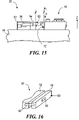
- FIG. 11 is a side view of the lithographic system, shown in FIG. 1 , with the docking system positioning the template transfer system to be in contact with the motion stage;
- FIG. 12 is a detailed view of the interface between the template transfer system and the motion stage shown in FIG. 11 ;
- FIG. 13 is a side view of the lithographic system shown in FIG. 1 , with the template transfer system coupled to the motion stage;
- FIG. 14 is a side view of the lithography system shown in FIG. 1 , with an arm of the docking system being retracted;
- FIG. 15 is a side view of the lithographic system shown in FIG. 1 , with the template transfer system having an orientation error;
- FIG. 16 is a perspective view of the docking system shown in FIG. 1 , having a protrusion positioned thereon;
- FIG. 17 is a side view of the lithographic system shown in FIG. 1 , with the template transfer system, having an orientation error, coupled to the docking system;
- FIG. 18 is a perspective view of the docking system shown in FIG. 1 , having a plurality of protrusions positioned thereon;
- FIG. 19 is a side view of the lithographic system shown in FIG. 1 , with the template transfer system having a latching system coupling the template transfer system to the docking system;
- FIG. 20 is a side view of the lithographic system shown in FIG. 1 , with the template transfer system having a latching system coupling the template transfer system to the motion stage.
- a system 10 to form a relief pattern in a substrate 12 includes a stage support 14 having a motion stage 16 , a template transfer system 18 , and a docking system 20 positioned thereon, with template transfer system 18 being positioned between motion stage 16 and docking system 20 .
- template transfer system 18 is coupled to docking system 20 .
- template transfer system 18 may be coupled to motion stage 16 , described further below.
- Motion stage 16 holds substrate 12 on a chuck 22 , with chuck 22 being any chuck including, but not limited to, vacuum and electromagnetic.
- a template 24 Spaced-apart from stage support 14 is a template 24 having a mold 26 with a patterning surface 28 thereon. Patterning surface 28 may be substantially smooth and/or planar, or may be patterned so that one or more recesses are formed therein.
- Template 24 is coupled to an imprint head 30 to facilitate movement of template 24 .
- a fluid dispense system 32 is coupled to be selectively placed in fluid communication with substrate 12 so as to deposit a polymerizable material 34 thereon. In a further embodiment, fluid dispense system 32 may be coupled to template transfer system 18 .
- a source 36 of energy 38 is coupled to direct energy 38 along a path 40 .
- Imprint head 30 and motion stage 16 are configured to arrange mold 26 and substrate 12 , respectively, to be in superimposition, and disposed in path 40 .
- An optical system 37 may facilitate obtaining a desired alignment of mold 26 and substrate 12 , described further below.
- Either imprint head 30 , motion stage 16 , or both vary a distance between mold 26 and substrate 12 to define a desired volume therebetween that is filled by polymerizable material 34 .
- polymerizable material 34 is disposed upon substrate 12 before the desired volume is defined between mold 26 and substrate 12 .
- polymerizable material 34 may fill the volume after the desired volume has been obtained.
- source 36 produces energy 38 , which causes polymerizable material 34 to solidify and/or cross-link, forming polymeric material conforming to the shape of the patterning surface 28 .
- Control of this process is regulated by a processor 42 that is in data communication with motion stage 16 , imprint head 30 , fluid dispense system 32 , source 36 , and optical system 37 operating on a computer readable program stored in a memory 44 .
- Motion stage 16 comprises a coupling system 46 to facilitate coupling with template transfer system 18 , described further below.
- Coupling system 46 comprises a coupling element 48 positioned on a side 50 of motion stage 16 , with side 50 facing template transfer system 18 .
- Coupling element 48 may extend a distance ‘d 1 ’ from side 50 and may have a geometrical shape selected from a flat plane, as shown in FIG. 2 , or a vee, as shown in FIG. 3 .
- the selection of the type of coupling design for coupling element 48 is known to one skilled in the art and typically depends on the specific application which is desired.
- coupling system 46 may comprise a plurality of coupling elements 48 , with the plurality of coupling elements 48 comprising any combination of the above-mentioned geometrical shapes.
- coupling system 46 comprises a pair of coupling elements 48 a and 48 b , as shown in FIG. 4 , with coupling element 48 a having a vee geometrical shape and coupling element 48 b having a flat plane geometrical shape.
- Motion stage 16 may comprise a plurality of air bearings (not shown) positioned between motion stage 16 and stage support 14 .
- the air bearings (not shown) allow frictionless motion of the same about stage support 14 .
- motion stage 16 may be in data communication with processor 42 operating on a computer readable program stored in memory 44 to regulate a motion thereof.
- docking system 20 comprises a docking body 52 coupled to a docking plate 54 by an arm 56 .
- Arm 56 may be in communication with a motor 58 .
- motor 58 may be a pneumatic actuator.
- Motor 58 translates arm 56 to place docking plate 54 in a desired position with respect to docking body 52 .
- a protrusion 62 Positioned on a side 60 of docking plate 54 is a protrusion 62 .
- Protrusion 62 may be employed to facilitate coupling of docking system 20 with template transfer system 18 , described further below.
- docking system 20 may be in data communication with processor 42 operating on a computer readable program stored in memory 44 to regulate a motion thereof.
- Template transfer system 18 comprises a body 64 having an optical detection system 66 , a template holder 68 , and a coupling means 70 positioned thereon.
- body 64 may comprise a component 71 , wherein component 71 may be any device that may interact with motion stage 16 , template transfer system 18 , docking system 20 , imprint head 30 , or any part of system 10 to produce a desired result.
- Body 64 has a first side 72 and a second side 74 , with first and second sides 72 and 74 being spaced-apart a distance ‘d 2 ’.
- First side 72 faces docking system 20 and second side 74 faces motion stage 16 .
- Coupling means 70 may extend a distance ‘d 3 ’ from second side 74 .
- Optical detection system 66 may comprise a microscope in optical communication with a camera.
- Coupling means 70 facilitates coupling of template transfer system 18 to motion stage 16 , described further below. As shown, coupling means 70 has a spherical geometry. However, in a further embodiment, coupling means 70 may have any geometry desired to facilitate coupling of template transfer system 18 to motion stage 16 .
- Template transfer system 18 may further comprise a plurality of air bearings (not shown) to allow frictionless motion of the same about stage support 14 .
- the plurality of air bearings (not shown) may be the same as those mentioned-above with respect to motion stage 16 .
- Template 24 may be removable from imprint head 30 of system 10 , and thus, another template may then be installed in imprint head 30 .
- another template may then be installed in imprint head 30 .
- template 24 may be stored on template transfer system 18 . More specifically, template 24 may be supported on template holder 68 of template transfer system 18 by a gas film, the gas film preventing contact between template 24 and template holder 68 .
- template holder 68 may comprise pins 76 having a first set 80 and a second set 82 .
- First set 80 and second set 82 may be spaced-apart diagonally from one another. Pins 76 facilitate a self aligning motion of template 24 .
- one set of first set 80 and second set 82 may be stationary while the remaining set of first set 80 and second set 82 may be moveable with respect to the stationary set of first set 80 and second set 82 .
- the stationary set of first set 80 and second set 82 provides a reference location upon template holder 68 to facilitate positioning of template 24 thereupon.
- first and second sets 80 and 82 may exert a force upon template 24 such that template 24 contacts the stationary set of first set 80 and second set 82 .
- each of first and second sets 80 and 82 each comprise two pins.
- each of first and second sets 80 and 82 may comprise any desired amount of pins to facilitate orientation of template 24 with respect to template holder 68 .
- template transfer system 18 is coupled to docking system 20 .
- template transfer system 18 comprises a cord 84 placing template transfer system 18 in communication with a coupling source 86 .
- coupling source 86 comprises a voltage source, as shown in FIG. 8 .
- an electric field may be created between template transfer system 18 and docking system 20 to couple template transfer system 18 to docking system 20 .
- coupling source 86 comprises a pump system, as shown in FIG. 9 .
- a vacuum may be created between template transfer system 18 and docking system 20 to couple template transfer system 18 to docking system 20 .
- cord 84 may also place template transfer system 18 in electrical communication with a power source (not shown).
- Control of coupling of template transfer system 18 may be regulated by processor 42 , shown in FIG. 1 , that is data communication with template transfer system 18 and coupling source 86 operating on a computer readable program stored in memory 44 , shown in FIG. 1 .
- template 24 may be positioned into a close proximity to imprint head 30 such that template 24 may be secured to imprint head 30 by vacuum and/or mechanical contact.
- template transfer system 18 may be coupled to motion stage 16 to position template 24 in a close proximity to imprint head 30 .
- motion stage 16 is translated such that the same is in a close proximity to template transfer system 18 .
- a collision between template transfer system 18 and motion stage 16 while translating motion stage 16 may result in, inter alia, structural comprise in system 10 , misalignment of template transfer system 18 with respect to motion stage 16 , and damage to template 24 and/or substrate 12 , shown in FIG. 1 , all of which are undesirable.
- a system and method to minimize, if not prevent, a probability of a collision between template transfer system 18 and motion stage 16 is described below.
- motion stage 16 is positioned proximate to template transfer system 18 .
- motion stage 16 has a range of motion associated therewith, i.e., a distance through which motion stage 16 may translate about stage support 14 .
- the range of motion of motion stage 16 has a periphery associated therewith, i.e., a maximum amount of distance motion stage 16 may translate about stage support 14 .
- motion stage 16 is translated to be spaced-apart a distance ‘d 4 ’ from surface 60 , shown in FIG. 5 , of docking plate 54 , with distance ‘d 4 ’ being at the periphery of the range of motion of motion stage 16 .
- Distance ‘d 4 ’ is greater than distance ‘d 2 ’ and thus, motion stage 16 is spaced-apart from template transfer system 18 defining a gap 88 therebetween.
- distance ‘d 4 ’ may be greater than the sum of distances ‘d 1 ’, ‘d 2 ’ and ‘d 3 ’, shown in FIG. 1 .
- gap 88 may be greater than the sum of distances ‘d 3 ’ and ‘d 1 ’, shown in FIG. 1 .
- motion stage 16 may be brought into a close proximity to template transfer system 18 while minimizing, if not preventing, a probability of a collision between motion stage 16 and template transfer system 18 while translating motion stage 16 .
- docking system 20 may position template transfer system 18 to be in contact with motion stage 16 . More specifically, arm 56 creates a gap 90 between docking body 52 and docking plate 54 , with docking plate 54 being positioned a distance ‘d 5 ’ from docking body 52 . Creation of gap 90 by arm 56 may be controlled by a force-controlled method wherein transmission of excessive force to motion stage 16 is minimized, if not prevented.
- template transfer system 18 may be positioned to be in contact with motion stage 16 .
- template transfer system 18 may be positioned in contact with motion stage 16 without causing translational motion of motion stage 16 .
- Template transfer system 18 may then be transferred from docking system 20 to motion stage 16 by coupling template transfer system 18 to motion stage 16 and decoupling template transfer system 18 from docking system 20 .
- coupling system 46 of motion stage 16 is brought into contact with coupling means 70 of template transfer system 18 to mate coupling system 46 with coupling means 70 to form a point of contact therebetween.
- Movement of template transfer system 18 may be constrained along a plurality of degrees of freedom depending on a type of coupling design employed for coupling system 46 .
- template transfer system 18 is decoupled from docking system 20 and coupled to motion stage 16 .
- coupling source 86 shown in FIG. 8
- coupling source 86 shown in FIG. 10
- template transfer system 18 may be translated about stage support 14 via motion stage 16 . More specifically, template transfer system 18 may be translated about stage support 14 to position template transfer system 18 in a desired position upon stage support 14 to facilitate coupling of template 24 to imprint head 30 .
- Optical detection system 66 may be employed in conjunction with optical system 37 , shown in FIG. 1 , to determine a presence and/or a position of template and/or template transfer system 18 with respect to imprint head 30 .
- Template 24 may then be coupled to imprint head 30 , with imprint head 30 having vacuum and/or mechanical retention means for holding template 24 , which are omitted for simplicity of illustration.
- arm 56 of docking system 20 may be subsequently retracted such that docking plate 54 is positioned adjacent to docking body 52 .
- arm 56 may be retracted concurrently during positioning of template transfer system 18 .
- the above-mentioned system and method of transferring template transfer system 18 between docking system 20 and motion stage 16 may be implemented with template transfer system 18 absent of template 24 .
- a second motion stage (not shown) differing from motion stage 16 may be employed to obtain a desired position of template transfer system 18 upon stage support 14 .
- template transfer system 18 may be transferred from motion stage 16 to docking system 20 by employing the above-mentioned process implemented in reverse. As a result, a probability of a collision between template transfer system 18 and docking system 20 while translating motion stage 16 may be minimized, if not prevented, which may be desired. Furthermore, transferring template transfer system 18 from motion stage 16 to docking system 20 minimizes a total mass that motion stage 16 may translate.
- Minimizing the total mass motion stage 16 may translate, and further, minimizing the inertial forces upon motion stage 16 , may result in, inter alia, improving a positioning precession of motion stage 16 , increasing a maximum velocity of motion stage 16 , increasing a maximum acceleration of motion stage 16 , and reducing step and settling times of motion stage 16 .
- a collision between template transfer system 18 and motion stage 16 may result in, inter alia, structural compromise in system 10 , misalignment of template transfer system 18 with respect to motion stage 16 , and damage to template 24 and/or substrate 12 , all of which are undesirable.
- minimizing the kinetic energy present during the collision between template transfer system 18 and motion stage 16 while translating motion stage 16 may minimize, if not prevent, the above-mentioned effects.
- motion stage 16 is positioned proximate to template transfer system 18 defining gap 88 , shown in FIG. 10 , therebetween.
- Docking system 20 then positions template transfer system 18 to be in contact with motion stage 16 .
- motion of template transfer system 18 and motion stage 16 occurs asynchronously. More specifically, translation of docking system 20 to place template transfer system 18 in contact with motion stage 16 , as mentioned above, does not occur until translation of motion stage 16 has ceased.
- only one of template transfer system 18 and motion stage 16 is moving at a time.
- the total kinetic energy of system 10 during translation of motion stage 16 may be reduced, which may be desired.
- minimizing the total mass motion stage 16 may translate may reduce the total kinetic energy of system 10 .
- the orientation error may be shown as first side 72 of template transfer system 18 forming an angle ⁇ with respect to a plane P 1 parallel to surface 60 of docking system 20 .
- docking plate 54 of docking system 20 comprises protrusion 62 .
- Protrusion 62 controls a point/line contact between docking plate 54 and template transfer system 18 . More specifically, when coupling template transfer system 18 to docking system 20 , protrusion 62 minimizes, if not prevents, pivoting motion of template transfer system 18 with respect to docking system 20 . As shown in FIG. 17 , template transfer system 18 is coupled to docking system 20 while maintaining the orientation error.
- protrusion 62 may also minimize a probability, if not prevent, of a collision between template transfer system 18 and stage support 14 during coupling of template transfer system 18 and docking system 20 .
- protrusion 62 may also abrogate rotation of template transfer system 18 about the Z-axis, which may be desired.
- docking plate 54 may comprise a plurality of protrusions 62 , as shown in FIG. 18 .
- template transfer system 18 may comprise a latching system 92 .
- Latching system 92 comprises latches 94 and 96 that may mechanically couple template transfer system 18 to docking system 20 and motion stage 16 , respectively.
- Latching system 92 may be implemented during, inter alia, power loss and/or vacuum loss of system 10 , shown in FIG. 1 .
- Latches 94 and 96 each comprise a shaft 98 having an end 100 and a coupling portion 102 having a pivot point 104 .
- Latches 94 and 96 may each pivot about their respective pivot points 104 . Ends 100 of latches 94 and 96 may extend beyond surfaces 72 and 74 , shown in FIGS. 1 and 5 , of template transfer system 18 , respectively.
- latch 94 is placed in a first position and latch 96 is placed in a second position.
- latching portion 102 of latch 94 makes mechanical contact with docking plate 54 to couple template transfer body 20 to docking system 20 .
- latch 96 is placed in the second position as a result of contact of end 100 of latch 96 with surface 60 , shown in FIG. 5 , of docking plate 54 . More specifically, upon contact of end 100 of latch 96 with surface 60 , shown in FIG. 5 , of docking plate 54 , shaft 98 translates such that latch 96 pivots about pivot point 104 placing latch 96 in the second position.
- latch 96 may be placed in the first position and latch 94 may be placed in the second position.
- latching portion 102 of latch 96 makes mechanical contact with motion stage 16 coupling template transfer system 20 to motion stage 16 .
- Positioning of latch 94 in the second position may be analogous to positioning latch 96 in the second position, as mentioned above with respect to FIG. 19 .
Abstract
Description
Claims (23)
Priority Applications (4)
| Application Number | Priority Date | Filing Date | Title |
|---|---|---|---|
| US11/211,766 US7665981B2 (en) | 2005-08-25 | 2005-08-25 | System to transfer a template transfer body between a motion stage and a docking plate |
| PCT/US2006/026366 WO2007024345A2 (en) | 2005-08-25 | 2006-07-06 | System to transfer a template transfer body between a motion stage and a docking plate |
| EP06786500A EP1934669A4 (en) | 2005-08-25 | 2006-07-06 | System to transfer a template transfer body between a motion stage and a docking plate |
| TW95125846A TWI309198B (en) | 2005-08-25 | 2006-07-14 | System to transfer a template transfer body between a motion stage and a docking plate |
Applications Claiming Priority (1)
| Application Number | Priority Date | Filing Date | Title |
|---|---|---|---|
| US11/211,766 US7665981B2 (en) | 2005-08-25 | 2005-08-25 | System to transfer a template transfer body between a motion stage and a docking plate |
Publications (2)
| Publication Number | Publication Date |
|---|---|
| US20070071582A1 US20070071582A1 (en) | 2007-03-29 |
| US7665981B2 true US7665981B2 (en) | 2010-02-23 |
Family
ID=37894198
Family Applications (1)
| Application Number | Title | Priority Date | Filing Date |
|---|---|---|---|
| US11/211,766 Active 2027-06-26 US7665981B2 (en) | 2005-08-25 | 2005-08-25 | System to transfer a template transfer body between a motion stage and a docking plate |
Country Status (1)
| Country | Link |
|---|---|
| US (1) | US7665981B2 (en) |
Cited By (3)
| Publication number | Priority date | Publication date | Assignee | Title |
|---|---|---|---|---|
| US20100237042A1 (en) * | 2009-03-23 | 2010-09-23 | Intevac, Inc. | Process for optimization of island to trench ratio in patterned media |
| US9811671B1 (en) | 2000-05-24 | 2017-11-07 | Copilot Ventures Fund Iii Llc | Authentication method and system |
| US9846814B1 (en) | 2008-04-23 | 2017-12-19 | Copilot Ventures Fund Iii Llc | Authentication method and system |
Families Citing this family (2)
| Publication number | Priority date | Publication date | Assignee | Title |
|---|---|---|---|---|
| US20070064384A1 (en) * | 2005-08-25 | 2007-03-22 | Molecular Imprints, Inc. | Method to transfer a template transfer body between a motion stage and a docking plate |
| KR20210118252A (en) * | 2016-09-30 | 2021-09-29 | 가부시키가이샤 니콘 | Object holding device, exposure device, flat-panel display manufacturing method, device manufacturing method, and object holding method |
Citations (114)
| Publication number | Priority date | Publication date | Assignee | Title |
|---|---|---|---|---|
| US4512848A (en) | 1984-02-06 | 1985-04-23 | Exxon Research And Engineering Co. | Procedure for fabrication of microstructures over large areas using physical replication |
| US4610442A (en) | 1982-10-19 | 1986-09-09 | Matsushita Electric Industrial Co, Ltd. | Positioning table |
| US4731155A (en) | 1987-04-15 | 1988-03-15 | General Electric Company | Process for forming a lithographic mask |
| US4760429A (en) * | 1986-11-05 | 1988-07-26 | The Perkin-Elmer Corporation | High speed reticle change system |
| US4763886A (en) | 1986-12-26 | 1988-08-16 | Nippon Thompson Co., Ltd. | XY-positioning table |
| US4848911A (en) | 1986-06-11 | 1989-07-18 | Kabushiki Kaisha Toshiba | Method for aligning first and second objects, relative to each other, and apparatus for practicing this method |
| US4959252A (en) | 1986-09-29 | 1990-09-25 | Rhone-Poulenc Chimie | Highly oriented thermotropic optical disc member |
| US5028366A (en) | 1988-01-12 | 1991-07-02 | Air Products And Chemicals, Inc. | Water based mold release compositions for making molded polyurethane foam |
| US5110514A (en) | 1989-05-01 | 1992-05-05 | Soane Technologies, Inc. | Controlled casting of a shrinkable material |
| US5148037A (en) | 1988-09-09 | 1992-09-15 | Canon Kabushiki Kaisha | Position detecting method and apparatus |
| US5151754A (en) | 1989-10-06 | 1992-09-29 | Kabushiki Kaisha Toshiba | Method and an apparatus for measuring a displacement between two objects and a method and an apparatus for measuring a gap distance between two objects |
| US5170182A (en) | 1990-08-23 | 1992-12-08 | Management Graphics, Inc. | Apparatus and method for registering an image on a recording medium |
| US5180757A (en) | 1987-12-16 | 1993-01-19 | Michael Lucey | Photopolymerizable compositions used in electronics |
| US5240550A (en) | 1990-09-21 | 1993-08-31 | U.S. Philips Corp. | Method of forming at least one groove in a substrate layer |
| US5259926A (en) | 1991-09-24 | 1993-11-09 | Hitachi, Ltd. | Method of manufacturing a thin-film pattern on a substrate |
| US5302627A (en) | 1990-12-28 | 1994-04-12 | Dow Corning Corporation | Method of indicating a cure point for ultraviolet radiation curing compositions by color change |
| US5332013A (en) | 1991-03-15 | 1994-07-26 | Shinko Electric Co., Ltd. | Unmanned conveying device in clean room |
| US5362940A (en) | 1990-11-09 | 1994-11-08 | Litel Instruments | Use of Fresnel zone plates for material processing |
| US5371822A (en) | 1992-06-09 | 1994-12-06 | Digital Equipment Corporation | Method of packaging and assembling opto-electronic integrated circuits |
| US5417537A (en) | 1993-05-07 | 1995-05-23 | Miller; Kenneth C. | Wafer transport device |
| US5425848A (en) | 1993-03-16 | 1995-06-20 | U.S. Philips Corporation | Method of providing a patterned relief of cured photoresist on a flat substrate surface and device for carrying out such a method |
| US5480047A (en) | 1993-06-04 | 1996-01-02 | Sharp Kabushiki Kaisha | Method for forming a fine resist pattern |
| US5512131A (en) | 1993-10-04 | 1996-04-30 | President And Fellows Of Harvard College | Formation of microstamped patterns on surfaces and derivative articles |
| US5545367A (en) | 1992-04-15 | 1996-08-13 | Soane Technologies, Inc. | Rapid prototype three dimensional stereolithography |
| US5601641A (en) | 1992-07-21 | 1997-02-11 | Tse Industries, Inc. | Mold release composition with polybutadiene and method of coating a mold core |
| US5669303A (en) | 1996-03-04 | 1997-09-23 | Motorola | Apparatus and method for stamping a surface |
| US5715064A (en) | 1994-06-17 | 1998-02-03 | International Business Machines Corporation | Step and repeat apparatus having enhanced accuracy and increased throughput |
| US5726548A (en) | 1992-12-18 | 1998-03-10 | Canon Kabushiki Kaisha | Moving stage apparatus and system using the same |
| US5760500A (en) | 1996-03-28 | 1998-06-02 | Nippon Thompson Co., Ltd. | XY table using a linear electromagnetic actuator |
| US5772905A (en) | 1995-11-15 | 1998-06-30 | Regents Of The University Of Minnesota | Nanoimprint lithography |
| US5776748A (en) | 1993-10-04 | 1998-07-07 | President And Fellows Of Harvard College | Method of formation of microstamped patterns on plates for adhesion of cells and other biological materials, devices and uses therefor |
| US5812629A (en) | 1997-04-30 | 1998-09-22 | Clauser; John F. | Ultrahigh resolution interferometric x-ray imaging |
| US5820769A (en) | 1995-05-24 | 1998-10-13 | Regents Of The University Of Minnesota | Method for making magnetic storage having discrete elements with quantized magnetic moments |
| US5849222A (en) | 1995-09-29 | 1998-12-15 | Johnson & Johnson Vision Products, Inc. | Method for reducing lens hole defects in production of contact lens blanks |
| US5849209A (en) | 1995-03-31 | 1998-12-15 | Johnson & Johnson Vision Products, Inc. | Mold material made with additives |
| US5858580A (en) | 1997-09-17 | 1999-01-12 | Numerical Technologies, Inc. | Phase shifting circuit manufacture method and apparatus |
| US5888650A (en) | 1996-06-03 | 1999-03-30 | Minnesota Mining And Manufacturing Company | Temperature-responsive adhesive article |
| US5905566A (en) | 1997-04-10 | 1999-05-18 | International Business Machines Corporation | Laser ablation top surface reference chuck |
| US5948470A (en) | 1997-04-28 | 1999-09-07 | Harrison; Christopher | Method of nanoscale patterning and products made thereby |
| US5969441A (en) | 1996-12-24 | 1999-10-19 | Asm Lithography Bv | Two-dimensionally balanced positioning device with two object holders, and lithographic device provided with such a positioning device |
| US5974150A (en) | 1997-09-30 | 1999-10-26 | Tracer Detection Technology Corp. | System and method for authentication of goods |
| US6046056A (en) | 1996-06-28 | 2000-04-04 | Caliper Technologies Corporation | High throughput screening assay systems in microscale fluidic devices |
| US6074827A (en) | 1996-07-30 | 2000-06-13 | Aclara Biosciences, Inc. | Microfluidic method for nucleic acid purification and processing |
| US6180239B1 (en) | 1993-10-04 | 2001-01-30 | President And Fellows Of Harvard College | Microcontact printing on surfaces and derivative articles |
| US6188150B1 (en) | 1999-06-16 | 2001-02-13 | Euv, Llc | Light weight high-stiffness stage platen |
| US6218316B1 (en) | 1998-10-22 | 2001-04-17 | Micron Technology, Inc. | Planarization of non-planar surfaces in device fabrication |
| US6262796B1 (en) | 1997-03-10 | 2001-07-17 | Asm Lithography B.V. | Positioning device having two object holders |
| US6274294B1 (en) | 1999-02-03 | 2001-08-14 | Electroformed Stents, Inc. | Cylindrical photolithography exposure process and apparatus |
| US6309580B1 (en) | 1995-11-15 | 2001-10-30 | Regents Of The University Of Minnesota | Release surfaces, particularly for use in nanoimprint lithography |
| US6326627B1 (en) | 2000-08-02 | 2001-12-04 | Archimedes Technology Group, Inc. | Mass filtering sputtered ion source |
| US6334960B1 (en) | 1999-03-11 | 2002-01-01 | Board Of Regents, The University Of Texas System | Step and flash imprint lithography |
| US6348999B1 (en) | 1995-05-10 | 2002-02-19 | Epigem Limited | Micro relief element and preparation thereof |
| US6355198B1 (en) | 1996-03-15 | 2002-03-12 | President And Fellows Of Harvard College | Method of forming articles including waveguides via capillary micromolding and microtransfer molding |
| US20020042027A1 (en) | 1998-10-09 | 2002-04-11 | Chou Stephen Y. | Microscale patterning and articles formed thereby |
| US6391217B2 (en) | 1999-12-23 | 2002-05-21 | University Of Massachusetts | Methods and apparatus for forming submicron patterns on films |
| US20020132482A1 (en) | 2000-07-18 | 2002-09-19 | Chou Stephen Y. | Fluid pressure imprint lithography |
| US20020150398A1 (en) | 2000-08-21 | 2002-10-17 | Choi Byung J. | Flexure based macro motion translation stage |
| US6467761B1 (en) | 1999-06-21 | 2002-10-22 | The United States Of America As Represented By The Secretary Of Commerce | Positioning stage |
| US6473157B2 (en) | 1992-02-07 | 2002-10-29 | Nikon Corporation | Method of manufacturing exposure apparatus and method for exposing a pattern on a mask onto a substrate |
| US20020168578A1 (en) | 1996-09-18 | 2002-11-14 | Numerical Technologies, Inc. | Phase shifting circuit manufacture method and apparatus |
| US20020170880A1 (en) | 2001-03-22 | 2002-11-21 | Yong Chen | Scanning probe based lithographic alignment |
| US6498350B2 (en) | 1999-12-21 | 2002-12-24 | Asml Netherlands B.V. | Crash prevention in positioning apparatus for use in lithographic projection apparatus |
| US6498640B1 (en) | 1999-12-30 | 2002-12-24 | Koninklijke Philips Electronics N.V. | Method to measure alignment using latent image grating structures |
| US6515736B1 (en) | 2000-05-04 | 2003-02-04 | International Business Machines Corporation | Reticle capturing and handling system |
| US20030025895A1 (en) | 2001-08-03 | 2003-02-06 | Michael Binnard | Apparatus and methods for detecting tool-induced shift in microlithography apparatus |
| US6518189B1 (en) | 1995-11-15 | 2003-02-11 | Regents Of The University Of Minnesota | Method and apparatus for high density nanostructures |
| US6517977B2 (en) | 2001-03-28 | 2003-02-11 | Motorola, Inc. | Lithographic template and method of formation and use |
| US6517995B1 (en) | 1999-09-14 | 2003-02-11 | Massachusetts Institute Of Technology | Fabrication of finely featured devices by liquid embossing |
| US20030062334A1 (en) | 2001-09-25 | 2003-04-03 | Lee Hong Hie | Method for forming a micro-pattern on a substrate by using capillary force |
| US20030080471A1 (en) | 2001-10-29 | 2003-05-01 | Chou Stephen Y. | Lithographic method for molding pattern with nanoscale features |
| US20030081193A1 (en) | 2001-06-01 | 2003-05-01 | White Donald L. | Holder, system, and process for improving overlay in lithography |
| US6580172B2 (en) | 2001-03-02 | 2003-06-17 | Motorola, Inc. | Lithographic template and method of formation and use |
| US20030137494A1 (en) | 2000-05-01 | 2003-07-24 | Tulbert David J. | Human-machine interface |
| US6621960B2 (en) | 2002-01-24 | 2003-09-16 | Oplink Communications, Inc. | Method of fabricating multiple superimposed fiber Bragg gratings |
| US20030174435A1 (en) | 2002-03-18 | 2003-09-18 | International Business Machines Corporation | Method and apparatus for providing an aligned coil for an inductive head structure using a patterned seed layer |
| US20030186140A1 (en) | 2001-06-27 | 2003-10-02 | Fries David P. | Maskless photolithography for using photoreactive agents |
| US6630988B2 (en) | 2001-06-28 | 2003-10-07 | Intel Corporation | Reticle stop block apparatus and method |
| US6646662B1 (en) | 1998-05-26 | 2003-11-11 | Seiko Epson Corporation | Patterning method, patterning apparatus, patterning template, and method for manufacturing the patterning template |
| US20030224295A1 (en) | 2002-03-01 | 2003-12-04 | Asml Netherlands, B.V. | Transfer method for a mask or substrate, storage box, apparatus adapted for use in such method, and device manufacturing method including such a transfer method |
| US6662725B1 (en) | 1999-09-17 | 2003-12-16 | Fuji Photo Film Co., Ltd. | Positioning method and positioning device for positioning printing plate relative to surface plate |
| US6696220B2 (en) | 2000-10-12 | 2004-02-24 | Board Of Regents, The University Of Texas System | Template for room temperature, low pressure micro-and nano-imprint lithography |
| US20040036201A1 (en) | 2000-07-18 | 2004-02-26 | Princeton University | Methods and apparatus of field-induced pressure imprint lithography |
| US20040046288A1 (en) | 2000-07-18 | 2004-03-11 | Chou Stephen Y. | Laset assisted direct imprint lithography |
| US6716754B2 (en) | 2002-03-12 | 2004-04-06 | Micron Technology, Inc. | Methods of forming patterns and molds for semiconductor constructions |
| US20040110856A1 (en) | 2002-12-04 | 2004-06-10 | Young Jung Gun | Polymer solution for nanoimprint lithography to reduce imprint temperature and pressure |
| US20040131718A1 (en) | 2000-07-18 | 2004-07-08 | Princeton University | Lithographic apparatus for fluid pressure imprint lithography |
| US20040137734A1 (en) | 1995-11-15 | 2004-07-15 | Princeton University | Compositions and processes for nanoimprinting |
| US20040156108A1 (en) | 2001-10-29 | 2004-08-12 | Chou Stephen Y. | Articles comprising nanoscale patterns with reduced edge roughness and methods of making same |
| US6776094B1 (en) | 1993-10-04 | 2004-08-17 | President & Fellows Of Harvard College | Kit For Microcontact Printing |
| US20040192041A1 (en) | 2003-03-27 | 2004-09-30 | Jun-Ho Jeong | UV nanoimprint lithography process using elementwise embossed stamp and selectively additive pressurization |
| US20040197843A1 (en) | 2001-07-25 | 2004-10-07 | Chou Stephen Y. | Nanochannel arrays and their preparation and use for high throughput macromolecular analysis |
| US6805054B1 (en) * | 2003-05-14 | 2004-10-19 | Molecular Imprints, Inc. | Method, system and holder for transferring templates during imprint lithography processes |
| WO2004103666A2 (en) | 2003-05-14 | 2004-12-02 | Molecular Imprints, Inc. | Method, system, holder and assembly for transferring templates during imprint lithography processes |
| US20040250945A1 (en) | 2003-06-10 | 2004-12-16 | Industrial Technology Research Institute | Method for and apparatus for bonding patterned imprint to a substrate by adhering means |
| US6842221B1 (en) * | 1999-03-12 | 2005-01-11 | Nikon Corporation | Exposure apparatus and exposure method, and device manufacturing method |
| EP1500980A1 (en) | 2003-07-22 | 2005-01-26 | ASML Netherlands B.V. | Lithographic apparatus, device manufacturing method, and device manufactured thereby |
| US6849558B2 (en) | 2002-05-22 | 2005-02-01 | The Board Of Trustees Of The Leland Stanford Junior University | Replication and transfer of microstructures and nanostructures |
| US20050037143A1 (en) | 2000-07-18 | 2005-02-17 | Chou Stephen Y. | Imprint lithography with improved monitoring and control and apparatus therefor |
| US6873087B1 (en) | 1999-10-29 | 2005-03-29 | Board Of Regents, The University Of Texas System | High precision orientation alignment and gap control stages for imprint lithography processes |
| US20050113484A1 (en) | 1997-05-23 | 2005-05-26 | Deco Patents, Inc. | Method and compositions for decorating glass |
| US6900881B2 (en) | 2002-07-11 | 2005-05-31 | Molecular Imprints, Inc. | Step and repeat imprint lithography systems |
| US6908861B2 (en) | 2002-07-11 | 2005-06-21 | Molecular Imprints, Inc. | Method for imprint lithography using an electric field |
| US6916584B2 (en) | 2002-08-01 | 2005-07-12 | Molecular Imprints, Inc. | Alignment methods for imprint lithography |
| US6916585B2 (en) | 2000-07-16 | 2005-07-12 | Board Of Regents, The University Of Texas Systems | Method of varying template dimensions to achieve alignment during imprint lithography |
| US6932934B2 (en) | 2002-07-11 | 2005-08-23 | Molecular Imprints, Inc. | Formation of discontinuous films during an imprint lithography process |
| US6964793B2 (en) | 2002-05-16 | 2005-11-15 | Board Of Regents, The University Of Texas System | Method for fabricating nanoscale patterns in light curable compositions using an electric field |
| US20050281638A1 (en) | 2004-05-24 | 2005-12-22 | Asml Netherlands B.V. | Insertion device, lithographic apparatus with said insertion device and device manufacturing method |
| US20060076717A1 (en) | 2002-07-11 | 2006-04-13 | Molecular Imprints, Inc. | Step and repeat imprint lithography processes |
| US7070405B2 (en) | 2002-08-01 | 2006-07-04 | Molecular Imprints, Inc. | Alignment systems for imprint lithography |
| US7128875B2 (en) | 1995-04-10 | 2006-10-31 | Cubicciotti Roger S | Signal processing devices comprising biological and bio-mimetic components |
| US20070064384A1 (en) | 2005-08-25 | 2007-03-22 | Molecular Imprints, Inc. | Method to transfer a template transfer body between a motion stage and a docking plate |
| US20070074635A1 (en) | 2005-08-25 | 2007-04-05 | Molecular Imprints, Inc. | System to couple a body and a docking plate |
| US7259102B2 (en) | 2005-09-30 | 2007-08-21 | Molecular Imprints, Inc. | Etching technique to planarize a multi-layer structure |
| US20090030547A1 (en) | 2003-11-13 | 2009-01-29 | Applied Materials, Inc. | Calibration of high speed loader to substrate transport system |
Family Cites Families (1)
| Publication number | Priority date | Publication date | Assignee | Title |
|---|---|---|---|---|
| US6236627B1 (en) * | 1998-12-17 | 2001-05-22 | Philips Electronics North America Corp. | Tracking method and track format based on quadrature wobble |
-
2005
- 2005-08-25 US US11/211,766 patent/US7665981B2/en active Active
Patent Citations (131)
| Publication number | Priority date | Publication date | Assignee | Title |
|---|---|---|---|---|
| US4610442A (en) | 1982-10-19 | 1986-09-09 | Matsushita Electric Industrial Co, Ltd. | Positioning table |
| US4512848A (en) | 1984-02-06 | 1985-04-23 | Exxon Research And Engineering Co. | Procedure for fabrication of microstructures over large areas using physical replication |
| US4848911A (en) | 1986-06-11 | 1989-07-18 | Kabushiki Kaisha Toshiba | Method for aligning first and second objects, relative to each other, and apparatus for practicing this method |
| US4959252A (en) | 1986-09-29 | 1990-09-25 | Rhone-Poulenc Chimie | Highly oriented thermotropic optical disc member |
| US4760429A (en) * | 1986-11-05 | 1988-07-26 | The Perkin-Elmer Corporation | High speed reticle change system |
| US4763886A (en) | 1986-12-26 | 1988-08-16 | Nippon Thompson Co., Ltd. | XY-positioning table |
| US4731155A (en) | 1987-04-15 | 1988-03-15 | General Electric Company | Process for forming a lithographic mask |
| US5180757A (en) | 1987-12-16 | 1993-01-19 | Michael Lucey | Photopolymerizable compositions used in electronics |
| US5028366A (en) | 1988-01-12 | 1991-07-02 | Air Products And Chemicals, Inc. | Water based mold release compositions for making molded polyurethane foam |
| US5148037A (en) | 1988-09-09 | 1992-09-15 | Canon Kabushiki Kaisha | Position detecting method and apparatus |
| US5110514A (en) | 1989-05-01 | 1992-05-05 | Soane Technologies, Inc. | Controlled casting of a shrinkable material |
| US5151754A (en) | 1989-10-06 | 1992-09-29 | Kabushiki Kaisha Toshiba | Method and an apparatus for measuring a displacement between two objects and a method and an apparatus for measuring a gap distance between two objects |
| US5170182A (en) | 1990-08-23 | 1992-12-08 | Management Graphics, Inc. | Apparatus and method for registering an image on a recording medium |
| US5240550A (en) | 1990-09-21 | 1993-08-31 | U.S. Philips Corp. | Method of forming at least one groove in a substrate layer |
| US5362940A (en) | 1990-11-09 | 1994-11-08 | Litel Instruments | Use of Fresnel zone plates for material processing |
| US5302627A (en) | 1990-12-28 | 1994-04-12 | Dow Corning Corporation | Method of indicating a cure point for ultraviolet radiation curing compositions by color change |
| US5332013A (en) | 1991-03-15 | 1994-07-26 | Shinko Electric Co., Ltd. | Unmanned conveying device in clean room |
| US5259926A (en) | 1991-09-24 | 1993-11-09 | Hitachi, Ltd. | Method of manufacturing a thin-film pattern on a substrate |
| US6473157B2 (en) | 1992-02-07 | 2002-10-29 | Nikon Corporation | Method of manufacturing exposure apparatus and method for exposing a pattern on a mask onto a substrate |
| US5545367A (en) | 1992-04-15 | 1996-08-13 | Soane Technologies, Inc. | Rapid prototype three dimensional stereolithography |
| US5371822A (en) | 1992-06-09 | 1994-12-06 | Digital Equipment Corporation | Method of packaging and assembling opto-electronic integrated circuits |
| US5601641A (en) | 1992-07-21 | 1997-02-11 | Tse Industries, Inc. | Mold release composition with polybutadiene and method of coating a mold core |
| US5726548A (en) | 1992-12-18 | 1998-03-10 | Canon Kabushiki Kaisha | Moving stage apparatus and system using the same |
| US5425848A (en) | 1993-03-16 | 1995-06-20 | U.S. Philips Corporation | Method of providing a patterned relief of cured photoresist on a flat substrate surface and device for carrying out such a method |
| US5417537A (en) | 1993-05-07 | 1995-05-23 | Miller; Kenneth C. | Wafer transport device |
| US5480047A (en) | 1993-06-04 | 1996-01-02 | Sharp Kabushiki Kaisha | Method for forming a fine resist pattern |
| US5512131A (en) | 1993-10-04 | 1996-04-30 | President And Fellows Of Harvard College | Formation of microstamped patterns on surfaces and derivative articles |
| US6180239B1 (en) | 1993-10-04 | 2001-01-30 | President And Fellows Of Harvard College | Microcontact printing on surfaces and derivative articles |
| US5776748A (en) | 1993-10-04 | 1998-07-07 | President And Fellows Of Harvard College | Method of formation of microstamped patterns on plates for adhesion of cells and other biological materials, devices and uses therefor |
| US6776094B1 (en) | 1993-10-04 | 2004-08-17 | President & Fellows Of Harvard College | Kit For Microcontact Printing |
| US5715064A (en) | 1994-06-17 | 1998-02-03 | International Business Machines Corporation | Step and repeat apparatus having enhanced accuracy and increased throughput |
| US5849209A (en) | 1995-03-31 | 1998-12-15 | Johnson & Johnson Vision Products, Inc. | Mold material made with additives |
| US7128875B2 (en) | 1995-04-10 | 2006-10-31 | Cubicciotti Roger S | Signal processing devices comprising biological and bio-mimetic components |
| US6348999B1 (en) | 1995-05-10 | 2002-02-19 | Epigem Limited | Micro relief element and preparation thereof |
| US5956216A (en) | 1995-05-24 | 1999-09-21 | Regents Of The University Of Minnesota | Magnetic storage having discrete elements with quantized magnetic moments |
| US5820769A (en) | 1995-05-24 | 1998-10-13 | Regents Of The University Of Minnesota | Method for making magnetic storage having discrete elements with quantized magnetic moments |
| US5849222A (en) | 1995-09-29 | 1998-12-15 | Johnson & Johnson Vision Products, Inc. | Method for reducing lens hole defects in production of contact lens blanks |
| US5772905A (en) | 1995-11-15 | 1998-06-30 | Regents Of The University Of Minnesota | Nanoimprint lithography |
| US6809356B2 (en) | 1995-11-15 | 2004-10-26 | Regents Of The University Of Minnesota | Method and apparatus for high density nanostructures |
| US20040137734A1 (en) | 1995-11-15 | 2004-07-15 | Princeton University | Compositions and processes for nanoimprinting |
| US6309580B1 (en) | 1995-11-15 | 2001-10-30 | Regents Of The University Of Minnesota | Release surfaces, particularly for use in nanoimprint lithography |
| US6518189B1 (en) | 1995-11-15 | 2003-02-11 | Regents Of The University Of Minnesota | Method and apparatus for high density nanostructures |
| US6828244B2 (en) | 1995-11-15 | 2004-12-07 | Regents Of The University Of Minnesota | Method and apparatus for high density nanostructures |
| US5669303A (en) | 1996-03-04 | 1997-09-23 | Motorola | Apparatus and method for stamping a surface |
| US6355198B1 (en) | 1996-03-15 | 2002-03-12 | President And Fellows Of Harvard College | Method of forming articles including waveguides via capillary micromolding and microtransfer molding |
| US5760500A (en) | 1996-03-28 | 1998-06-02 | Nippon Thompson Co., Ltd. | XY table using a linear electromagnetic actuator |
| US5888650A (en) | 1996-06-03 | 1999-03-30 | Minnesota Mining And Manufacturing Company | Temperature-responsive adhesive article |
| US6046056A (en) | 1996-06-28 | 2000-04-04 | Caliper Technologies Corporation | High throughput screening assay systems in microscale fluidic devices |
| US6074827A (en) | 1996-07-30 | 2000-06-13 | Aclara Biosciences, Inc. | Microfluidic method for nucleic acid purification and processing |
| US20020168578A1 (en) | 1996-09-18 | 2002-11-14 | Numerical Technologies, Inc. | Phase shifting circuit manufacture method and apparatus |
| US5969441A (en) | 1996-12-24 | 1999-10-19 | Asm Lithography Bv | Two-dimensionally balanced positioning device with two object holders, and lithographic device provided with such a positioning device |
| US6262796B1 (en) | 1997-03-10 | 2001-07-17 | Asm Lithography B.V. | Positioning device having two object holders |
| US5905566A (en) | 1997-04-10 | 1999-05-18 | International Business Machines Corporation | Laser ablation top surface reference chuck |
| US5948470A (en) | 1997-04-28 | 1999-09-07 | Harrison; Christopher | Method of nanoscale patterning and products made thereby |
| US5812629A (en) | 1997-04-30 | 1998-09-22 | Clauser; John F. | Ultrahigh resolution interferometric x-ray imaging |
| US20050113484A1 (en) | 1997-05-23 | 2005-05-26 | Deco Patents, Inc. | Method and compositions for decorating glass |
| US5858580A (en) | 1997-09-17 | 1999-01-12 | Numerical Technologies, Inc. | Phase shifting circuit manufacture method and apparatus |
| US5974150A (en) | 1997-09-30 | 1999-10-26 | Tracer Detection Technology Corp. | System and method for authentication of goods |
| US6646662B1 (en) | 1998-05-26 | 2003-11-11 | Seiko Epson Corporation | Patterning method, patterning apparatus, patterning template, and method for manufacturing the patterning template |
| US20030034329A1 (en) | 1998-06-30 | 2003-02-20 | Chou Stephen Y. | Lithographic method for molding pattern with nanoscale depth |
| US20020167117A1 (en) | 1998-06-30 | 2002-11-14 | Regents Of The University Of Minnesota | Release surfaces, particularly for use in nanoimprint lithography |
| US20020042027A1 (en) | 1998-10-09 | 2002-04-11 | Chou Stephen Y. | Microscale patterning and articles formed thereby |
| US6713238B1 (en) | 1998-10-09 | 2004-03-30 | Stephen Y. Chou | Microscale patterning and articles formed thereby |
| US20040118809A1 (en) | 1998-10-09 | 2004-06-24 | Chou Stephen Y. | Microscale patterning and articles formed thereby |
| US6218316B1 (en) | 1998-10-22 | 2001-04-17 | Micron Technology, Inc. | Planarization of non-planar surfaces in device fabrication |
| US6274294B1 (en) | 1999-02-03 | 2001-08-14 | Electroformed Stents, Inc. | Cylindrical photolithography exposure process and apparatus |
| US6334960B1 (en) | 1999-03-11 | 2002-01-01 | Board Of Regents, The University Of Texas System | Step and flash imprint lithography |
| US6842221B1 (en) * | 1999-03-12 | 2005-01-11 | Nikon Corporation | Exposure apparatus and exposure method, and device manufacturing method |
| US6188150B1 (en) | 1999-06-16 | 2001-02-13 | Euv, Llc | Light weight high-stiffness stage platen |
| US6467761B1 (en) | 1999-06-21 | 2002-10-22 | The United States Of America As Represented By The Secretary Of Commerce | Positioning stage |
| US6517995B1 (en) | 1999-09-14 | 2003-02-11 | Massachusetts Institute Of Technology | Fabrication of finely featured devices by liquid embossing |
| US6662725B1 (en) | 1999-09-17 | 2003-12-16 | Fuji Photo Film Co., Ltd. | Positioning method and positioning device for positioning printing plate relative to surface plate |
| US6873087B1 (en) | 1999-10-29 | 2005-03-29 | Board Of Regents, The University Of Texas System | High precision orientation alignment and gap control stages for imprint lithography processes |
| US6498350B2 (en) | 1999-12-21 | 2002-12-24 | Asml Netherlands B.V. | Crash prevention in positioning apparatus for use in lithographic projection apparatus |
| US6391217B2 (en) | 1999-12-23 | 2002-05-21 | University Of Massachusetts | Methods and apparatus for forming submicron patterns on films |
| US6498640B1 (en) | 1999-12-30 | 2002-12-24 | Koninklijke Philips Electronics N.V. | Method to measure alignment using latent image grating structures |
| US20030137494A1 (en) | 2000-05-01 | 2003-07-24 | Tulbert David J. | Human-machine interface |
| US6515736B1 (en) | 2000-05-04 | 2003-02-04 | International Business Machines Corporation | Reticle capturing and handling system |
| US6916585B2 (en) | 2000-07-16 | 2005-07-12 | Board Of Regents, The University Of Texas Systems | Method of varying template dimensions to achieve alignment during imprint lithography |
| US20040046288A1 (en) | 2000-07-18 | 2004-03-11 | Chou Stephen Y. | Laset assisted direct imprint lithography |
| US20050037143A1 (en) | 2000-07-18 | 2005-02-17 | Chou Stephen Y. | Imprint lithography with improved monitoring and control and apparatus therefor |
| US6482742B1 (en) | 2000-07-18 | 2002-11-19 | Stephen Y. Chou | Fluid pressure imprint lithography |
| US6946360B2 (en) | 2000-07-18 | 2005-09-20 | Nanonex Corporation | Fluid pressure bonding |
| US20040131718A1 (en) | 2000-07-18 | 2004-07-08 | Princeton University | Lithographic apparatus for fluid pressure imprint lithography |
| US20020132482A1 (en) | 2000-07-18 | 2002-09-19 | Chou Stephen Y. | Fluid pressure imprint lithography |
| US20040036201A1 (en) | 2000-07-18 | 2004-02-26 | Princeton University | Methods and apparatus of field-induced pressure imprint lithography |
| US6326627B1 (en) | 2000-08-02 | 2001-12-04 | Archimedes Technology Group, Inc. | Mass filtering sputtered ion source |
| US20020150398A1 (en) | 2000-08-21 | 2002-10-17 | Choi Byung J. | Flexure based macro motion translation stage |
| US6696220B2 (en) | 2000-10-12 | 2004-02-24 | Board Of Regents, The University Of Texas System | Template for room temperature, low pressure micro-and nano-imprint lithography |
| US6580172B2 (en) | 2001-03-02 | 2003-06-17 | Motorola, Inc. | Lithographic template and method of formation and use |
| US20020170880A1 (en) | 2001-03-22 | 2002-11-21 | Yong Chen | Scanning probe based lithographic alignment |
| US6955767B2 (en) | 2001-03-22 | 2005-10-18 | Hewlett-Packard Development Company, Lp. | Scanning probe based lithographic alignment |
| US6517977B2 (en) | 2001-03-28 | 2003-02-11 | Motorola, Inc. | Lithographic template and method of formation and use |
| US20030081193A1 (en) | 2001-06-01 | 2003-05-01 | White Donald L. | Holder, system, and process for improving overlay in lithography |
| US20030186140A1 (en) | 2001-06-27 | 2003-10-02 | Fries David P. | Maskless photolithography for using photoreactive agents |
| US6630988B2 (en) | 2001-06-28 | 2003-10-07 | Intel Corporation | Reticle stop block apparatus and method |
| US20040197843A1 (en) | 2001-07-25 | 2004-10-07 | Chou Stephen Y. | Nanochannel arrays and their preparation and use for high throughput macromolecular analysis |
| US20030025895A1 (en) | 2001-08-03 | 2003-02-06 | Michael Binnard | Apparatus and methods for detecting tool-induced shift in microlithography apparatus |
| US6678038B2 (en) | 2001-08-03 | 2004-01-13 | Nikon Corporation | Apparatus and methods for detecting tool-induced shift in microlithography apparatus |
| US20030062334A1 (en) | 2001-09-25 | 2003-04-03 | Lee Hong Hie | Method for forming a micro-pattern on a substrate by using capillary force |
| US20030080471A1 (en) | 2001-10-29 | 2003-05-01 | Chou Stephen Y. | Lithographic method for molding pattern with nanoscale features |
| US20040156108A1 (en) | 2001-10-29 | 2004-08-12 | Chou Stephen Y. | Articles comprising nanoscale patterns with reduced edge roughness and methods of making same |
| US20030080472A1 (en) | 2001-10-29 | 2003-05-01 | Chou Stephen Y. | Lithographic method with bonded release layer for molding small patterns |
| US6621960B2 (en) | 2002-01-24 | 2003-09-16 | Oplink Communications, Inc. | Method of fabricating multiple superimposed fiber Bragg gratings |
| US20030224295A1 (en) | 2002-03-01 | 2003-12-04 | Asml Netherlands, B.V. | Transfer method for a mask or substrate, storage box, apparatus adapted for use in such method, and device manufacturing method including such a transfer method |
| US6716754B2 (en) | 2002-03-12 | 2004-04-06 | Micron Technology, Inc. | Methods of forming patterns and molds for semiconductor constructions |
| US7117583B2 (en) | 2002-03-18 | 2006-10-10 | International Business Machines Corporation | Method and apparatus using a pre-patterned seed layer for providing an aligned coil for an inductive head structure |
| US20030174435A1 (en) | 2002-03-18 | 2003-09-18 | International Business Machines Corporation | Method and apparatus for providing an aligned coil for an inductive head structure using a patterned seed layer |
| US6964793B2 (en) | 2002-05-16 | 2005-11-15 | Board Of Regents, The University Of Texas System | Method for fabricating nanoscale patterns in light curable compositions using an electric field |
| US6849558B2 (en) | 2002-05-22 | 2005-02-01 | The Board Of Trustees Of The Leland Stanford Junior University | Replication and transfer of microstructures and nanostructures |
| US20060077374A1 (en) | 2002-07-11 | 2006-04-13 | Molecular Imprints, Inc. | Step and repeat imprint lithography systems |
| US20060076717A1 (en) | 2002-07-11 | 2006-04-13 | Molecular Imprints, Inc. | Step and repeat imprint lithography processes |
| US6900881B2 (en) | 2002-07-11 | 2005-05-31 | Molecular Imprints, Inc. | Step and repeat imprint lithography systems |
| US6908861B2 (en) | 2002-07-11 | 2005-06-21 | Molecular Imprints, Inc. | Method for imprint lithography using an electric field |
| US20060062867A1 (en) | 2002-07-11 | 2006-03-23 | Molecular Imprints, Inc. | Formation of discontinuous films during an imprint lithography process |
| US7077992B2 (en) | 2002-07-11 | 2006-07-18 | Molecular Imprints, Inc. | Step and repeat imprint lithography processes |
| US6932934B2 (en) | 2002-07-11 | 2005-08-23 | Molecular Imprints, Inc. | Formation of discontinuous films during an imprint lithography process |
| US7070405B2 (en) | 2002-08-01 | 2006-07-04 | Molecular Imprints, Inc. | Alignment systems for imprint lithography |
| US6916584B2 (en) | 2002-08-01 | 2005-07-12 | Molecular Imprints, Inc. | Alignment methods for imprint lithography |
| US20040110856A1 (en) | 2002-12-04 | 2004-06-10 | Young Jung Gun | Polymer solution for nanoimprint lithography to reduce imprint temperature and pressure |
| US20040192041A1 (en) | 2003-03-27 | 2004-09-30 | Jun-Ho Jeong | UV nanoimprint lithography process using elementwise embossed stamp and selectively additive pressurization |
| US6805054B1 (en) * | 2003-05-14 | 2004-10-19 | Molecular Imprints, Inc. | Method, system and holder for transferring templates during imprint lithography processes |
| WO2004103666A2 (en) | 2003-05-14 | 2004-12-02 | Molecular Imprints, Inc. | Method, system, holder and assembly for transferring templates during imprint lithography processes |
| US20040250945A1 (en) | 2003-06-10 | 2004-12-16 | Industrial Technology Research Institute | Method for and apparatus for bonding patterned imprint to a substrate by adhering means |
| EP1500980A1 (en) | 2003-07-22 | 2005-01-26 | ASML Netherlands B.V. | Lithographic apparatus, device manufacturing method, and device manufactured thereby |
| US7423733B2 (en) * | 2003-07-22 | 2008-09-09 | Asml Netherlands B.V. | Lithographic apparatus, device manufacturing method, and device manufactured thereby with docking system for positioning a patterning device |
| US20090030547A1 (en) | 2003-11-13 | 2009-01-29 | Applied Materials, Inc. | Calibration of high speed loader to substrate transport system |
| US20050281638A1 (en) | 2004-05-24 | 2005-12-22 | Asml Netherlands B.V. | Insertion device, lithographic apparatus with said insertion device and device manufacturing method |
| US20070064384A1 (en) | 2005-08-25 | 2007-03-22 | Molecular Imprints, Inc. | Method to transfer a template transfer body between a motion stage and a docking plate |
| US20070074635A1 (en) | 2005-08-25 | 2007-04-05 | Molecular Imprints, Inc. | System to couple a body and a docking plate |
| US7259102B2 (en) | 2005-09-30 | 2007-08-21 | Molecular Imprints, Inc. | Etching technique to planarize a multi-layer structure |
Non-Patent Citations (34)
| Title |
|---|
| Abstract of Japanese patent 02-192045, Jul. 27, 1990. |
| Abstract of Japanese Patent 02-24848, Jan. 26, 1990. |
| Abstract of Japanese Patent 02-92603, Aug. 12, 2004. |
| Bailey et al., Step and Flash Imprint Lithography: Defect Analysis, Journal of Vacuum Science, B 19(6), pp. 2806-2810 Nov. 1, 2001. |
| Bailey et al., Step and Flash Imprint Lithography: Template Surface Treatment and Defect Analysis, Journal of Vacuum Science, B 18(6), pp. 3572-3577 Nov. 1, 2000. |
| Choi et al., Design of Orientation Stages for Step and Flash Imprint Lithography, Precision Engineering, pp. 192-199 Jan. 1, 2001. |
| Choi et al., Partially Contstrained Compliant Stages for High Resolution Imprint Lithography, 2000 Proceedings of the ASME 2000 Design Engineering Technical Conference, DETC2000/MECH-4145, Baltimore, Maryland. Sep. 10, 2000. |
| Chou et al., Imprint Lithography with 25-Nanometer Resolution, Science vol. 272, pp. 85-87 Apr. 5, 1996. |
| Chou et al., Imprint Lithography with Sub-10 nm Feature Size and High Throughput, Microelectronic Engineering 35, pp. 237-240 Jan. 1, 1997. |
| Chou et al., Imprint of Sub-25 nm Vias and Trenches in Polymers, Appl. Phys. Lett. 67 (21) Nov. 20, 1995. |
| Chou et al., Lithographically Induced Self-assembly of Periodic Polymer Micropillar Arrays, J. Vac. Sci. Technol. B 17 (6), pp. 3197-3202 Nov. 1, 1999. |
| Chou et al., Nanoimprint Lithography, Journal of Vacuum Science Technolgoy B 14(16), pp. 4129-4133 Nov. 1, 1996. |
| Chou et al., Ultrafast and Direct Imprint of Nanostructures in Silicon, Nature, col. 417, (Jun. 2002), pp. 835-837 Jun. 1, 2002. |
| Chou, Nanoimprint Lithography and Lithographically Induced Self-Assembly, MRS Bulletin, pp. 512-517 Jul. 1, 2001. |
| Colburn et al., Characterization and Modeling of Volumetric and Mechanical Properties for Step and Flash Imprint Lithography Photopolymers, Journal of Vacuum Science Technology. vol. b. 19(6) Nov. 1, 2001. |
| Colburn et al., Development and Advantages of Step-and-Flash Lithography, Solid State Technology Jul. 1, 2001. |
| Colburn et al., Dissertation for the Degree of Doctor of Philosophy, Step and Flash Imprint Lithography: A Low-Pressure, Room-Temperature Nanoimprint Lithography Aug. 1, 2001. |
| Colburn et al., Step and Flash Imprint Lithography for sub-100 nm Patterning, Proceedings of SPIE vol. 3997, pp. 453-457 Jan. 1, 2000. |
| Colburn et al., Step and Flash Imprint Lithography: A New Approach to High-Resolution Patterning, Proc. Of SPIE, vol. 3676 Mar. 1, 1999. |
| Haisma et al., Mold-assisted Nanolithography: A Process for Reliable Pattern Replication, J. Vac. Sci. Technol. B, pp. 4124-4128 Nov. 1, 1996. |
| Heidari, Nanoimprint Lithography at the 6 in. Wafer Scale, J. Vac. Sci. Technol. B 18(6), pp. 3557-3560 Nov. 1, 2000. |
| Huang et al., Reversal Imprinting by Transferring Polymer from Mold to Substrate, J. Vac. Sc. Technol. B 20(6); pp. 2872-2876 Nov. 1, 2002. |
| Johnson et al., Advances in Step and Flash Imprint Lithography, SPIE Microlithography Conference Feb. 23, 2003. |
| Kim et al., High-precision Magnetic Levitation Stage for Photolithography, Precision Engineering. vol. 22. No. 2, pp. 66-77 Apr. 1, 1998. |
| Lee et al., Ultraprecision Stage for Alignment of Wafers in Advanced Microlithography, Precision Engineering, pp. 113-122 Sep. 1, 1997. |
| Nguyen, Asymmetric Fluid-Structure Dynamics in Nanoscale Imprint Lithography, The University of Texas at Austin, pp. 1-111 Aug. 1, 2001. |
| PCT/US06/26366 International Search Report, Aug. 14, 2008. |
| Schneider et al., Stripes of Partially Fluorinated Alkyl Chains: Dipolar Langmuir Monolayers, J. Chem. Phys. vol. 122, Issue 9 Mar. 1, 2005. |
| Translation of Japanese Patent 02-24848, Jan. 26, 1990. |
| Translation of Japanese Patent 02-92603, Apr. 3, 1990. |
| U.S. Appl. No. 11/211,763, Schumaker et al. entitled Method to Transfer a Template Transfer Body Between a Motion Stage and a Docking Plate, filed Aug. 25, 2005. |
| U.S. Appl. No. 11/211,785, Schumaker et al. entitled System to Couple a Body and a Docking Plate, filed Aug. 25, 2005. |
| Williams et al., Magnetic Levitation Scanning Stage for Extreme Ultraviolet Lithography, American Society for Precision Engineering, vol. 20, pp. 583-586 Nov. 1, 1999. |
| Xia et al., Soft Lithography, Angew. Chem. Int. Ed., pp. 550-575 Jan. 1, 1998. |
Cited By (8)
| Publication number | Priority date | Publication date | Assignee | Title |
|---|---|---|---|---|
| US9811671B1 (en) | 2000-05-24 | 2017-11-07 | Copilot Ventures Fund Iii Llc | Authentication method and system |
| US9846814B1 (en) | 2008-04-23 | 2017-12-19 | Copilot Ventures Fund Iii Llc | Authentication method and system |
| US10275675B1 (en) | 2008-04-23 | 2019-04-30 | Copilot Ventures Fund Iii Llc | Authentication method and system |
| US11200439B1 (en) | 2008-04-23 | 2021-12-14 | Copilot Ventures Fund Iii Llc | Authentication method and system |
| US11600056B2 (en) | 2008-04-23 | 2023-03-07 | CoPilot Ventures III LLC | Authentication method and system |
| US11924356B2 (en) | 2008-04-23 | 2024-03-05 | Copilot Ventures Fund Iii Llc | Authentication method and system |
| US20100237042A1 (en) * | 2009-03-23 | 2010-09-23 | Intevac, Inc. | Process for optimization of island to trench ratio in patterned media |
| US8715515B2 (en) | 2009-03-23 | 2014-05-06 | Intevac, Inc. | Process for optimization of island to trench ratio in patterned media |
Also Published As
| Publication number | Publication date |
|---|---|
| US20070071582A1 (en) | 2007-03-29 |
Similar Documents
| Publication | Publication Date | Title |
|---|---|---|
| US8387482B2 (en) | Method and system to control movement of a body for nano-scale manufacturing | |
| US7670529B2 (en) | Method and system for double-sided patterning of substrates | |
| US20090037004A1 (en) | Method and System to Control Movement of a Body for Nano-Scale Manufacturing | |
| EP1240550B1 (en) | A process for separating a template from a substrate during imprint lithography, and associated imprint lithography process | |
| US7170589B2 (en) | Apparatus to vary dimensions of a substrate during nano-scale manufacturing | |
| US7387508B2 (en) | Compliant device for nano-scale manufacturing | |
| US20050263077A1 (en) | Adaptive shape substrate support method | |
| US20100015270A1 (en) | Inner cavity system for nano-imprint lithography | |
| EP1973719A2 (en) | Patterning substrates employing multiple chucks | |
| US7665981B2 (en) | System to transfer a template transfer body between a motion stage and a docking plate | |
| US20070231422A1 (en) | System to vary dimensions of a thin template | |
| JP2009200345A (en) | Processing apparatus | |
| US20070074635A1 (en) | System to couple a body and a docking plate | |
| US20070064384A1 (en) | Method to transfer a template transfer body between a motion stage and a docking plate | |
| WO2007024345A2 (en) | System to transfer a template transfer body between a motion stage and a docking plate | |
| JP2021141259A (en) | Determination method, imprint method, imprint apparatus, article manufacturing method, and program | |
| Meissl et al. | Precision Flexure Mechanisms in High Speed Nanopatterning Systems |
Legal Events
| Date | Code | Title | Description |
|---|---|---|---|
| AS | Assignment |
Owner name: MOLECULAR IMPRINTS, INC.,TEXAS Free format text: ASSIGNMENT OF ASSIGNORS INTEREST;ASSIGNORS:SCHUMAKER, PHILIP D.;FANCELLO, ANGELO;KIM, JAE H.;AND OTHERS;REEL/FRAME:016613/0771 Effective date: 20050823 Owner name: MOLECULAR IMPRINTS, INC., TEXAS Free format text: ASSIGNMENT OF ASSIGNORS INTEREST;ASSIGNORS:SCHUMAKER, PHILIP D.;FANCELLO, ANGELO;KIM, JAE H.;AND OTHERS;REEL/FRAME:016613/0771 Effective date: 20050823 |
|
| FEPP | Fee payment procedure |
Free format text: PAYOR NUMBER ASSIGNED (ORIGINAL EVENT CODE: ASPN); ENTITY STATUS OF PATENT OWNER: LARGE ENTITY |
|
| STCF | Information on status: patent grant |
Free format text: PATENTED CASE |
|
| CC | Certificate of correction | ||
| AS | Assignment |
Owner name: CANON INC., JAPAN Free format text: ASSIGNMENT OF ASSIGNORS INTEREST;ASSIGNOR:MOLECULAR IMPRINTS, INC.;REEL/FRAME:026842/0929 Effective date: 20110901 |
|
| AS | Assignment |
Owner name: CANON INC., JAPAN Free format text: CORRECTIVE ASSIGNMENT TO CORRECT THE NATURE OF CONVEYANCE FROM AN "ASSIGNMENT" TO "SECURITY AGREEMENT" PREVIOUSLY RECORDED ON REEL 026842 FRAME 0929. ASSIGNOR(S) HEREBY CONFIRMS THE THE ORIGINAL DOCUMENT SUBMITTED WAS A "SECURITY AGREEMENT";ASSIGNOR:MOLECULAR IMPRINTS, INC.;REEL/FRAME:031003/0031 Effective date: 20110901 |
|
| FPAY | Fee payment |
Year of fee payment: 4 |
|
| AS | Assignment |
Owner name: CANON INC., JAPAN Free format text: RELEASE OF SECURITY INTEREST;ASSIGNOR:MOLECULAR IMPRINTS, INC.;REEL/FRAME:033161/0705 Effective date: 20140613 |
|
| AS | Assignment |
Owner name: MOLECULAR IMPRINTS, INC., TEXAS Free format text: CORRECTIVE ASSIGNMENT TO CORRECT THE ASSIGNOR AND ASSIGNEE PREVIOUSLY RECORDED ON REEL 033161 FRAME 0705. ASSIGNOR(S) HEREBY CONFIRMS THE ASSIGNMENT;ASSIGNOR:CANON INC.;REEL/FRAME:033227/0398 Effective date: 20140613 |
|
| AS | Assignment |
Owner name: MII NEWCO, INC., TEXAS Free format text: ASSIGNMENT OF JOINT OWNERSHIP;ASSIGNOR:MOLECULAR IMPRINTS, INC.;REEL/FRAME:033329/0280 Effective date: 20140710 |
|
| AS | Assignment |
Owner name: CANON NANOTECHNOLOGIES, INC., TEXAS Free format text: CHANGE OF NAME;ASSIGNOR:MOLECULAR IMPRINTS, INC.;REEL/FRAME:033400/0184 Effective date: 20140417 |
|
| AS | Assignment |
Owner name: MOLECULAR IMPRINTS, INC., TEXAS Free format text: CHANGE OF NAME;ASSIGNOR:MII NEWCO, INC.;REEL/FRAME:033449/0684 Effective date: 20140423 |
|
| AS | Assignment |
Owner name: MOLECULAR IMPRINTS, INC., TEXAS Free format text: CONFIRMATORY ASSIGNMENT OF JOINT PATENT OWNERSHIP;ASSIGNOR:CANON NANOTECHNOLOGIES, INC.;REEL/FRAME:035507/0559 Effective date: 20150427 |
|
| MAFP | Maintenance fee payment |
Free format text: PAYMENT OF MAINTENANCE FEE, 8TH YEAR, LARGE ENTITY (ORIGINAL EVENT CODE: M1552) Year of fee payment: 8 |
|
| AS | Assignment |
Owner name: JP MORGAN CHASE BANK, N.A., NEW YORK Free format text: PATENT SECURITY AGREEMENT;ASSIGNORS:MAGIC LEAP, INC.;MOLECULAR IMPRINTS, INC.;MENTOR ACQUISITION ONE, LLC;REEL/FRAME:050138/0287 Effective date: 20190820 |
|
| AS | Assignment |
Owner name: CITIBANK, N.A., NEW YORK Free format text: ASSIGNMENT OF SECURITY INTEREST IN PATENTS;ASSIGNOR:JPMORGAN CHASE BANK, N.A.;REEL/FRAME:050967/0138 Effective date: 20191106 |
|
| MAFP | Maintenance fee payment |
Free format text: PAYMENT OF MAINTENANCE FEE, 12TH YEAR, LARGE ENTITY (ORIGINAL EVENT CODE: M1553); ENTITY STATUS OF PATENT OWNER: LARGE ENTITY Year of fee payment: 12 |