US7700421B2 - Semiconductor device and method for manufacturing the same - Google Patents
Semiconductor device and method for manufacturing the same Download PDFInfo
- Publication number
- US7700421B2 US7700421B2 US12/175,481 US17548108A US7700421B2 US 7700421 B2 US7700421 B2 US 7700421B2 US 17548108 A US17548108 A US 17548108A US 7700421 B2 US7700421 B2 US 7700421B2
- Authority
- US
- United States
- Prior art keywords
- semiconductor
- region
- semiconductor film
- regions
- substrate
- Prior art date
- Legal status (The legal status is an assumption and is not a legal conclusion. Google has not performed a legal analysis and makes no representation as to the accuracy of the status listed.)
- Expired - Fee Related
Links
- 239000004065 semiconductor Substances 0.000 title claims abstract description 96
- 238000000034 method Methods 0.000 title claims description 41
- 238000004519 manufacturing process Methods 0.000 title claims description 23
- 239000000758 substrate Substances 0.000 claims abstract description 59
- 239000011159 matrix material Substances 0.000 claims abstract description 42
- 239000013078 crystal Substances 0.000 claims abstract description 41
- 238000002425 crystallisation Methods 0.000 claims abstract description 31
- 230000008025 crystallization Effects 0.000 claims abstract description 31
- 229910052751 metal Inorganic materials 0.000 claims abstract description 27
- 239000002184 metal Substances 0.000 claims abstract description 27
- 229910052759 nickel Inorganic materials 0.000 claims description 56
- 230000002093 peripheral effect Effects 0.000 claims description 38
- 239000012535 impurity Substances 0.000 claims description 24
- 239000000463 material Substances 0.000 claims description 19
- 238000000059 patterning Methods 0.000 claims description 13
- 239000007788 liquid Substances 0.000 claims description 11
- 229910052697 platinum Inorganic materials 0.000 claims description 7
- 229910052787 antimony Inorganic materials 0.000 claims description 6
- 229910052785 arsenic Inorganic materials 0.000 claims description 6
- 239000003990 capacitor Substances 0.000 claims description 6
- 229910052802 copper Inorganic materials 0.000 claims description 6
- 229910052737 gold Inorganic materials 0.000 claims description 6
- 229910052738 indium Inorganic materials 0.000 claims description 6
- 230000001678 irradiating effect Effects 0.000 claims description 6
- 229910052763 palladium Inorganic materials 0.000 claims description 6
- 229910052698 phosphorus Inorganic materials 0.000 claims description 6
- 229910052709 silver Inorganic materials 0.000 claims description 6
- 229910052718 tin Inorganic materials 0.000 claims description 6
- 238000010438 heat treatment Methods 0.000 claims 5
- 239000003054 catalyst Substances 0.000 abstract description 35
- 230000012010 growth Effects 0.000 abstract description 32
- 229910021417 amorphous silicon Inorganic materials 0.000 abstract description 19
- 239000004973 liquid crystal related substance Substances 0.000 abstract description 14
- 230000001737 promoting effect Effects 0.000 abstract description 6
- 239000010408 film Substances 0.000 description 125
- PXHVJJICTQNCMI-UHFFFAOYSA-N Nickel Chemical compound [Ni] PXHVJJICTQNCMI-UHFFFAOYSA-N 0.000 description 101
- XUIMIQQOPSSXEZ-UHFFFAOYSA-N Silicon Chemical compound [Si] XUIMIQQOPSSXEZ-UHFFFAOYSA-N 0.000 description 33
- 229910052710 silicon Inorganic materials 0.000 description 33
- 239000010703 silicon Substances 0.000 description 33
- VYPSYNLAJGMNEJ-UHFFFAOYSA-N Silicium dioxide Chemical compound O=[Si]=O VYPSYNLAJGMNEJ-UHFFFAOYSA-N 0.000 description 27
- 229910052814 silicon oxide Inorganic materials 0.000 description 27
- 239000000243 solution Substances 0.000 description 26
- 239000010410 layer Substances 0.000 description 16
- 238000000137 annealing Methods 0.000 description 15
- 238000005268 plasma chemical vapour deposition Methods 0.000 description 11
- 239000010409 thin film Substances 0.000 description 11
- 229910021419 crystalline silicon Inorganic materials 0.000 description 10
- LYCAIKOWRPUZTN-UHFFFAOYSA-N Ethylene glycol Chemical compound OCCO LYCAIKOWRPUZTN-UHFFFAOYSA-N 0.000 description 9
- 229910052782 aluminium Inorganic materials 0.000 description 9
- XAGFODPZIPBFFR-UHFFFAOYSA-N aluminium Chemical compound [Al] XAGFODPZIPBFFR-UHFFFAOYSA-N 0.000 description 9
- 239000010407 anodic oxide Substances 0.000 description 9
- 239000000969 carrier Substances 0.000 description 8
- 238000000576 coating method Methods 0.000 description 8
- 239000012298 atmosphere Substances 0.000 description 7
- 230000000694 effects Effects 0.000 description 7
- 239000011248 coating agent Substances 0.000 description 6
- 239000011229 interlayer Substances 0.000 description 6
- 150000002500 ions Chemical class 0.000 description 6
- 230000003647 oxidation Effects 0.000 description 6
- 238000007254 oxidation reaction Methods 0.000 description 6
- BOTDANWDWHJENH-UHFFFAOYSA-N Tetraethyl orthosilicate Chemical compound CCO[Si](OCC)(OCC)OCC BOTDANWDWHJENH-UHFFFAOYSA-N 0.000 description 5
- 238000010586 diagram Methods 0.000 description 5
- 230000001965 increasing effect Effects 0.000 description 5
- 238000004544 sputter deposition Methods 0.000 description 5
- 150000001242 acetic acid derivatives Chemical class 0.000 description 4
- 230000015572 biosynthetic process Effects 0.000 description 4
- 239000002019 doping agent Substances 0.000 description 4
- 239000007789 gas Substances 0.000 description 4
- 239000011521 glass Substances 0.000 description 4
- 150000002816 nickel compounds Chemical class 0.000 description 4
- RUFLMLWJRZAWLJ-UHFFFAOYSA-N nickel silicide Chemical compound [Ni]=[Si]=[Ni] RUFLMLWJRZAWLJ-UHFFFAOYSA-N 0.000 description 4
- 229910021334 nickel silicide Inorganic materials 0.000 description 4
- 239000012266 salt solution Substances 0.000 description 4
- 238000004528 spin coating Methods 0.000 description 4
- QGZKDVFQNNGYKY-UHFFFAOYSA-O Ammonium Chemical compound [NH4+] QGZKDVFQNNGYKY-UHFFFAOYSA-O 0.000 description 3
- UHOVQNZJYSORNB-UHFFFAOYSA-N Benzene Chemical compound C1=CC=CC=C1 UHOVQNZJYSORNB-UHFFFAOYSA-N 0.000 description 3
- UFHFLCQGNIYNRP-UHFFFAOYSA-N Hydrogen Chemical compound [H][H] UFHFLCQGNIYNRP-UHFFFAOYSA-N 0.000 description 3
- XYFCBTPGUUZFHI-UHFFFAOYSA-N Phosphine Chemical compound P XYFCBTPGUUZFHI-UHFFFAOYSA-N 0.000 description 3
- FEWJPZIEWOKRBE-UHFFFAOYSA-N Tartaric acid Natural products [H+].[H+].[O-]C(=O)C(O)C(O)C([O-])=O FEWJPZIEWOKRBE-UHFFFAOYSA-N 0.000 description 3
- NRTOMJZYCJJWKI-UHFFFAOYSA-N Titanium nitride Chemical compound [Ti]#N NRTOMJZYCJJWKI-UHFFFAOYSA-N 0.000 description 3
- YXFVVABEGXRONW-UHFFFAOYSA-N Toluene Chemical compound CC1=CC=CC=C1 YXFVVABEGXRONW-UHFFFAOYSA-N 0.000 description 3
- 230000001133 acceleration Effects 0.000 description 3
- MQRWBMAEBQOWAF-UHFFFAOYSA-N acetic acid;nickel Chemical compound [Ni].CC(O)=O.CC(O)=O MQRWBMAEBQOWAF-UHFFFAOYSA-N 0.000 description 3
- QVGXLLKOCUKJST-UHFFFAOYSA-N atomic oxygen Chemical compound [O] QVGXLLKOCUKJST-UHFFFAOYSA-N 0.000 description 3
- 230000002950 deficient Effects 0.000 description 3
- 238000001312 dry etching Methods 0.000 description 3
- 230000006870 function Effects 0.000 description 3
- BHEPBYXIRTUNPN-UHFFFAOYSA-N hydridophosphorus(.) (triplet) Chemical compound [PH] BHEPBYXIRTUNPN-UHFFFAOYSA-N 0.000 description 3
- 239000001257 hydrogen Substances 0.000 description 3
- 229910052739 hydrogen Inorganic materials 0.000 description 3
- AMGQUBHHOARCQH-UHFFFAOYSA-N indium;oxotin Chemical compound [In].[Sn]=O AMGQUBHHOARCQH-UHFFFAOYSA-N 0.000 description 3
- 239000007769 metal material Substances 0.000 description 3
- 229940078494 nickel acetate Drugs 0.000 description 3
- 239000001301 oxygen Substances 0.000 description 3
- 229910052760 oxygen Inorganic materials 0.000 description 3
- BASFCYQUMIYNBI-UHFFFAOYSA-N platinum Chemical compound [Pt] BASFCYQUMIYNBI-UHFFFAOYSA-N 0.000 description 3
- 229920001721 polyimide Polymers 0.000 description 3
- 229910052706 scandium Inorganic materials 0.000 description 3
- SIXSYDAISGFNSX-UHFFFAOYSA-N scandium atom Chemical compound [Sc] SIXSYDAISGFNSX-UHFFFAOYSA-N 0.000 description 3
- 235000002906 tartaric acid Nutrition 0.000 description 3
- 239000011975 tartaric acid Substances 0.000 description 3
- XLYOFNOQVPJJNP-UHFFFAOYSA-N water Substances O XLYOFNOQVPJJNP-UHFFFAOYSA-N 0.000 description 3
- HEDRZPFGACZZDS-UHFFFAOYSA-N Chloroform Chemical compound ClC(Cl)Cl HEDRZPFGACZZDS-UHFFFAOYSA-N 0.000 description 2
- RTZKZFJDLAIYFH-UHFFFAOYSA-N Diethyl ether Chemical compound CCOCC RTZKZFJDLAIYFH-UHFFFAOYSA-N 0.000 description 2
- 230000004913 activation Effects 0.000 description 2
- 239000003795 chemical substances by application Substances 0.000 description 2
- 230000003247 decreasing effect Effects 0.000 description 2
- 230000007547 defect Effects 0.000 description 2
- 238000001035 drying Methods 0.000 description 2
- 238000005530 etching Methods 0.000 description 2
- 238000001704 evaporation Methods 0.000 description 2
- 230000008020 evaporation Effects 0.000 description 2
- 238000004518 low pressure chemical vapour deposition Methods 0.000 description 2
- 230000004048 modification Effects 0.000 description 2
- 238000012986 modification Methods 0.000 description 2
- BMGNSKKZFQMGDH-FDGPNNRMSA-L nickel(2+);(z)-4-oxopent-2-en-2-olate Chemical compound [Ni+2].C\C([O-])=C\C(C)=O.C\C([O-])=C\C(C)=O BMGNSKKZFQMGDH-FDGPNNRMSA-L 0.000 description 2
- 239000012299 nitrogen atmosphere Substances 0.000 description 2
- 238000009832 plasma treatment Methods 0.000 description 2
- 239000002798 polar solvent Substances 0.000 description 2
- 239000007858 starting material Substances 0.000 description 2
- VZGDMQKNWNREIO-UHFFFAOYSA-N tetrachloromethane Chemical compound ClC(Cl)(Cl)Cl VZGDMQKNWNREIO-UHFFFAOYSA-N 0.000 description 2
- 238000005406 washing Methods 0.000 description 2
- OCOCFNMFLNFNIA-ZSCHJXSPSA-N 2-(1-benzylindazol-3-yl)oxyacetic acid;(2s)-2,6-diaminohexanoic acid Chemical compound [NH3+]CCCC[C@H]([NH3+])C([O-])=O.C12=CC=CC=C2C(OCC(=O)[O-])=NN1CC1=CC=CC=C1 OCOCFNMFLNFNIA-ZSCHJXSPSA-N 0.000 description 1
- XRBQEYWBWZFUIJ-UHFFFAOYSA-N 2-ethylhexanoic acid;nickel Chemical compound [Ni].CCCCC(CC)C(O)=O XRBQEYWBWZFUIJ-UHFFFAOYSA-N 0.000 description 1
- QTBSBXVTEAMEQO-UHFFFAOYSA-M Acetate Chemical compound CC([O-])=O QTBSBXVTEAMEQO-UHFFFAOYSA-M 0.000 description 1
- IJGRMHOSHXDMSA-UHFFFAOYSA-N Atomic nitrogen Chemical compound N#N IJGRMHOSHXDMSA-UHFFFAOYSA-N 0.000 description 1
- MYMOFIZGZYHOMD-UHFFFAOYSA-N Dioxygen Chemical compound O=O MYMOFIZGZYHOMD-UHFFFAOYSA-N 0.000 description 1
- LFQSCWFLJHTTHZ-UHFFFAOYSA-N Ethanol Chemical compound CCO LFQSCWFLJHTTHZ-UHFFFAOYSA-N 0.000 description 1
- 229910021586 Nickel(II) chloride Inorganic materials 0.000 description 1
- CTQNGGLPUBDAKN-UHFFFAOYSA-N O-Xylene Chemical compound CC1=CC=CC=C1C CTQNGGLPUBDAKN-UHFFFAOYSA-N 0.000 description 1
- 239000002253 acid Substances 0.000 description 1
- 230000005540 biological transmission Effects 0.000 description 1
- 238000006243 chemical reaction Methods 0.000 description 1
- 238000004140 cleaning Methods 0.000 description 1
- 238000009792 diffusion process Methods 0.000 description 1
- 229910001873 dinitrogen Inorganic materials 0.000 description 1
- 229910001882 dioxygen Inorganic materials 0.000 description 1
- 230000003028 elevating effect Effects 0.000 description 1
- 239000000839 emulsion Substances 0.000 description 1
- 238000002474 experimental method Methods 0.000 description 1
- 229910021472 group 8 element Inorganic materials 0.000 description 1
- QMMRZOWCJAIUJA-UHFFFAOYSA-L nickel dichloride Chemical compound Cl[Ni]Cl QMMRZOWCJAIUJA-UHFFFAOYSA-L 0.000 description 1
- 229910000480 nickel oxide Inorganic materials 0.000 description 1
- LGQLOGILCSXPEA-UHFFFAOYSA-L nickel sulfate Chemical compound [Ni+2].[O-]S([O-])(=O)=O LGQLOGILCSXPEA-UHFFFAOYSA-L 0.000 description 1
- UQPSGBZICXWIAG-UHFFFAOYSA-L nickel(2+);dibromide;trihydrate Chemical compound O.O.O.Br[Ni]Br UQPSGBZICXWIAG-UHFFFAOYSA-L 0.000 description 1
- HZPNKQREYVVATQ-UHFFFAOYSA-L nickel(2+);diformate Chemical compound [Ni+2].[O-]C=O.[O-]C=O HZPNKQREYVVATQ-UHFFFAOYSA-L 0.000 description 1
- DOLZKNFSRCEOFV-UHFFFAOYSA-L nickel(2+);oxalate Chemical compound [Ni+2].[O-]C(=O)C([O-])=O DOLZKNFSRCEOFV-UHFFFAOYSA-L 0.000 description 1
- 229910000008 nickel(II) carbonate Inorganic materials 0.000 description 1
- 229910000363 nickel(II) sulfate Inorganic materials 0.000 description 1
- ZULUUIKRFGGGTL-UHFFFAOYSA-L nickel(ii) carbonate Chemical compound [Ni+2].[O-]C([O-])=O ZULUUIKRFGGGTL-UHFFFAOYSA-L 0.000 description 1
- BFDHFSHZJLFAMC-UHFFFAOYSA-L nickel(ii) hydroxide Chemical compound [OH-].[OH-].[Ni+2] BFDHFSHZJLFAMC-UHFFFAOYSA-L 0.000 description 1
- BFSQJYRFLQUZKX-UHFFFAOYSA-L nickel(ii) iodide Chemical compound I[Ni]I BFSQJYRFLQUZKX-UHFFFAOYSA-L 0.000 description 1
- KBJMLQFLOWQJNF-UHFFFAOYSA-N nickel(ii) nitrate Chemical compound [Ni+2].[O-][N+]([O-])=O.[O-][N+]([O-])=O KBJMLQFLOWQJNF-UHFFFAOYSA-N 0.000 description 1
- 239000012454 non-polar solvent Substances 0.000 description 1
- GNRSAWUEBMWBQH-UHFFFAOYSA-N oxonickel Chemical compound [Ni]=O GNRSAWUEBMWBQH-UHFFFAOYSA-N 0.000 description 1
- 239000000843 powder Substances 0.000 description 1
- 230000008569 process Effects 0.000 description 1
- 230000004044 response Effects 0.000 description 1
- 239000002904 solvent Substances 0.000 description 1
- 238000001179 sorption measurement Methods 0.000 description 1
- 238000007669 thermal treatment Methods 0.000 description 1
- 238000009281 ultraviolet germicidal irradiation Methods 0.000 description 1
- 238000009736 wetting Methods 0.000 description 1
- 239000008096 xylene Substances 0.000 description 1
Images


Classifications
-
- H—ELECTRICITY
- H01—ELECTRIC ELEMENTS
- H01L—SEMICONDUCTOR DEVICES NOT COVERED BY CLASS H10
- H01L21/00—Processes or apparatus adapted for the manufacture or treatment of semiconductor or solid state devices or of parts thereof
- H01L21/02—Manufacture or treatment of semiconductor devices or of parts thereof
- H01L21/02104—Forming layers
- H01L21/02365—Forming inorganic semiconducting materials on a substrate
- H01L21/02656—Special treatments
- H01L21/02664—Aftertreatments
- H01L21/02667—Crystallisation or recrystallisation of non-monocrystalline semiconductor materials, e.g. regrowth
- H01L21/02672—Crystallisation or recrystallisation of non-monocrystalline semiconductor materials, e.g. regrowth using crystallisation enhancing elements
-
- H—ELECTRICITY
- H01—ELECTRIC ELEMENTS
- H01L—SEMICONDUCTOR DEVICES NOT COVERED BY CLASS H10
- H01L21/00—Processes or apparatus adapted for the manufacture or treatment of semiconductor or solid state devices or of parts thereof
- H01L21/02—Manufacture or treatment of semiconductor devices or of parts thereof
- H01L21/04—Manufacture or treatment of semiconductor devices or of parts thereof the devices having at least one potential-jump barrier or surface barrier, e.g. PN junction, depletion layer or carrier concentration layer
- H01L21/18—Manufacture or treatment of semiconductor devices or of parts thereof the devices having at least one potential-jump barrier or surface barrier, e.g. PN junction, depletion layer or carrier concentration layer the devices having semiconductor bodies comprising elements of Group IV of the Periodic System or AIIIBV compounds with or without impurities, e.g. doping materials
-
- A—HUMAN NECESSITIES
- A61—MEDICAL OR VETERINARY SCIENCE; HYGIENE
- A61B—DIAGNOSIS; SURGERY; IDENTIFICATION
- A61B18/00—Surgical instruments, devices or methods for transferring non-mechanical forms of energy to or from the body
- A61B18/18—Surgical instruments, devices or methods for transferring non-mechanical forms of energy to or from the body by applying electromagnetic radiation, e.g. microwaves
- A61B18/20—Surgical instruments, devices or methods for transferring non-mechanical forms of energy to or from the body by applying electromagnetic radiation, e.g. microwaves using laser
-
- B—PERFORMING OPERATIONS; TRANSPORTING
- B23—MACHINE TOOLS; METAL-WORKING NOT OTHERWISE PROVIDED FOR
- B23K—SOLDERING OR UNSOLDERING; WELDING; CLADDING OR PLATING BY SOLDERING OR WELDING; CUTTING BY APPLYING HEAT LOCALLY, e.g. FLAME CUTTING; WORKING BY LASER BEAM
- B23K26/00—Working by laser beam, e.g. welding, cutting or boring
- B23K26/08—Devices involving relative movement between laser beam and workpiece
-
- H—ELECTRICITY
- H01—ELECTRIC ELEMENTS
- H01L—SEMICONDUCTOR DEVICES NOT COVERED BY CLASS H10
- H01L21/00—Processes or apparatus adapted for the manufacture or treatment of semiconductor or solid state devices or of parts thereof
- H01L21/02—Manufacture or treatment of semiconductor devices or of parts thereof
- H01L21/02104—Forming layers
- H01L21/02365—Forming inorganic semiconducting materials on a substrate
- H01L21/02518—Deposited layers
- H01L21/02521—Materials
- H01L21/02524—Group 14 semiconducting materials
- H01L21/02532—Silicon, silicon germanium, germanium
-
- H—ELECTRICITY
- H01—ELECTRIC ELEMENTS
- H01L—SEMICONDUCTOR DEVICES NOT COVERED BY CLASS H10
- H01L21/00—Processes or apparatus adapted for the manufacture or treatment of semiconductor or solid state devices or of parts thereof
- H01L21/02—Manufacture or treatment of semiconductor devices or of parts thereof
- H01L21/02104—Forming layers
- H01L21/02365—Forming inorganic semiconducting materials on a substrate
- H01L21/02656—Special treatments
- H01L21/02664—Aftertreatments
- H01L21/02667—Crystallisation or recrystallisation of non-monocrystalline semiconductor materials, e.g. regrowth
- H01L21/02675—Crystallisation or recrystallisation of non-monocrystalline semiconductor materials, e.g. regrowth using laser beams
- H01L21/02686—Pulsed laser beam
-
- H—ELECTRICITY
- H01—ELECTRIC ELEMENTS
- H01L—SEMICONDUCTOR DEVICES NOT COVERED BY CLASS H10
- H01L27/00—Devices consisting of a plurality of semiconductor or other solid-state components formed in or on a common substrate
- H01L27/02—Devices consisting of a plurality of semiconductor or other solid-state components formed in or on a common substrate including semiconductor components specially adapted for rectifying, oscillating, amplifying or switching and having at least one potential-jump barrier or surface barrier; including integrated passive circuit elements with at least one potential-jump barrier or surface barrier
- H01L27/12—Devices consisting of a plurality of semiconductor or other solid-state components formed in or on a common substrate including semiconductor components specially adapted for rectifying, oscillating, amplifying or switching and having at least one potential-jump barrier or surface barrier; including integrated passive circuit elements with at least one potential-jump barrier or surface barrier the substrate being other than a semiconductor body, e.g. an insulating body
- H01L27/1214—Devices consisting of a plurality of semiconductor or other solid-state components formed in or on a common substrate including semiconductor components specially adapted for rectifying, oscillating, amplifying or switching and having at least one potential-jump barrier or surface barrier; including integrated passive circuit elements with at least one potential-jump barrier or surface barrier the substrate being other than a semiconductor body, e.g. an insulating body comprising a plurality of TFTs formed on a non-semiconducting substrate, e.g. driving circuits for AMLCDs
- H01L27/1259—Multistep manufacturing methods
- H01L27/127—Multistep manufacturing methods with a particular formation, treatment or patterning of the active layer specially adapted to the circuit arrangement
- H01L27/1274—Multistep manufacturing methods with a particular formation, treatment or patterning of the active layer specially adapted to the circuit arrangement using crystallisation of amorphous semiconductor or recrystallisation of crystalline semiconductor
- H01L27/1277—Multistep manufacturing methods with a particular formation, treatment or patterning of the active layer specially adapted to the circuit arrangement using crystallisation of amorphous semiconductor or recrystallisation of crystalline semiconductor using a crystallisation promoting species, e.g. local introduction of Ni catalyst
-
- H—ELECTRICITY
- H01—ELECTRIC ELEMENTS
- H01L—SEMICONDUCTOR DEVICES NOT COVERED BY CLASS H10
- H01L29/00—Semiconductor devices adapted for rectifying, amplifying, oscillating or switching, or capacitors or resistors with at least one potential-jump barrier or surface barrier, e.g. PN junction depletion layer or carrier concentration layer; Details of semiconductor bodies or of electrodes thereof ; Multistep manufacturing processes therefor
- H01L29/02—Semiconductor bodies ; Multistep manufacturing processes therefor
- H01L29/04—Semiconductor bodies ; Multistep manufacturing processes therefor characterised by their crystalline structure, e.g. polycrystalline, cubic or particular orientation of crystalline planes
-
- H—ELECTRICITY
- H01—ELECTRIC ELEMENTS
- H01L—SEMICONDUCTOR DEVICES NOT COVERED BY CLASS H10
- H01L29/00—Semiconductor devices adapted for rectifying, amplifying, oscillating or switching, or capacitors or resistors with at least one potential-jump barrier or surface barrier, e.g. PN junction depletion layer or carrier concentration layer; Details of semiconductor bodies or of electrodes thereof ; Multistep manufacturing processes therefor
- H01L29/66—Types of semiconductor device ; Multistep manufacturing processes therefor
- H01L29/66007—Multistep manufacturing processes
- H01L29/66075—Multistep manufacturing processes of devices having semiconductor bodies comprising group 14 or group 13/15 materials
- H01L29/66227—Multistep manufacturing processes of devices having semiconductor bodies comprising group 14 or group 13/15 materials the devices being controllable only by the electric current supplied or the electric potential applied, to an electrode which does not carry the current to be rectified, amplified or switched, e.g. three-terminal devices
- H01L29/66409—Unipolar field-effect transistors
- H01L29/66477—Unipolar field-effect transistors with an insulated gate, i.e. MISFET
- H01L29/66742—Thin film unipolar transistors
- H01L29/6675—Amorphous silicon or polysilicon transistors
- H01L29/66757—Lateral single gate single channel transistors with non-inverted structure, i.e. the channel layer is formed before the gate
-
- H—ELECTRICITY
- H01—ELECTRIC ELEMENTS
- H01L—SEMICONDUCTOR DEVICES NOT COVERED BY CLASS H10
- H01L29/00—Semiconductor devices adapted for rectifying, amplifying, oscillating or switching, or capacitors or resistors with at least one potential-jump barrier or surface barrier, e.g. PN junction depletion layer or carrier concentration layer; Details of semiconductor bodies or of electrodes thereof ; Multistep manufacturing processes therefor
- H01L29/66—Types of semiconductor device ; Multistep manufacturing processes therefor
- H01L29/68—Types of semiconductor device ; Multistep manufacturing processes therefor controllable by only the electric current supplied, or only the electric potential applied, to an electrode which does not carry the current to be rectified, amplified or switched
- H01L29/76—Unipolar devices, e.g. field effect transistors
- H01L29/772—Field effect transistors
- H01L29/78—Field effect transistors with field effect produced by an insulated gate
- H01L29/786—Thin film transistors, i.e. transistors with a channel being at least partly a thin film
- H01L29/78606—Thin film transistors, i.e. transistors with a channel being at least partly a thin film with supplementary region or layer in the thin film or in the insulated bulk substrate supporting it for controlling or increasing the safety of the device
- H01L29/78618—Thin film transistors, i.e. transistors with a channel being at least partly a thin film with supplementary region or layer in the thin film or in the insulated bulk substrate supporting it for controlling or increasing the safety of the device characterised by the drain or the source properties, e.g. the doping structure, the composition, the sectional shape or the contact structure
- H01L29/78621—Thin film transistors, i.e. transistors with a channel being at least partly a thin film with supplementary region or layer in the thin film or in the insulated bulk substrate supporting it for controlling or increasing the safety of the device characterised by the drain or the source properties, e.g. the doping structure, the composition, the sectional shape or the contact structure with LDD structure or an extension or an offset region or characterised by the doping profile
-
- A—HUMAN NECESSITIES
- A61—MEDICAL OR VETERINARY SCIENCE; HYGIENE
- A61B—DIAGNOSIS; SURGERY; IDENTIFICATION
- A61B18/00—Surgical instruments, devices or methods for transferring non-mechanical forms of energy to or from the body
- A61B18/18—Surgical instruments, devices or methods for transferring non-mechanical forms of energy to or from the body by applying electromagnetic radiation, e.g. microwaves
- A61B18/20—Surgical instruments, devices or methods for transferring non-mechanical forms of energy to or from the body by applying electromagnetic radiation, e.g. microwaves using laser
- A61B2018/2035—Beam shaping or redirecting; Optical components therefor
- A61B2018/20351—Scanning mechanisms
- A61B2018/20359—Scanning mechanisms by movable mirrors, e.g. galvanometric
-
- H—ELECTRICITY
- H01—ELECTRIC ELEMENTS
- H01L—SEMICONDUCTOR DEVICES NOT COVERED BY CLASS H10
- H01L29/00—Semiconductor devices adapted for rectifying, amplifying, oscillating or switching, or capacitors or resistors with at least one potential-jump barrier or surface barrier, e.g. PN junction depletion layer or carrier concentration layer; Details of semiconductor bodies or of electrodes thereof ; Multistep manufacturing processes therefor
- H01L29/66—Types of semiconductor device ; Multistep manufacturing processes therefor
- H01L29/68—Types of semiconductor device ; Multistep manufacturing processes therefor controllable by only the electric current supplied, or only the electric potential applied, to an electrode which does not carry the current to be rectified, amplified or switched
- H01L29/76—Unipolar devices, e.g. field effect transistors
- H01L29/772—Field effect transistors
- H01L29/78—Field effect transistors with field effect produced by an insulated gate
- H01L29/786—Thin film transistors, i.e. transistors with a channel being at least partly a thin film
- H01L29/78651—Silicon transistors
- H01L29/7866—Non-monocrystalline silicon transistors
- H01L29/78672—Polycrystalline or microcrystalline silicon transistor
- H01L29/78675—Polycrystalline or microcrystalline silicon transistor with normal-type structure, e.g. with top gate
Definitions
- the present invention relates to an active-matrix type liquid crystal device or thin film integrated circuit devices using a semiconductor layer with crystallinity.
- TFT thin film transistors
- a peripheral circuit member is constituted by IC and is externally connected to terminals of matrix wirings of the pixels. Further, it is also known to form TFTs for forming a peripheral circuit on the same substrate on which TFTs are arranged in a matrix as a switching element in a pixel region.
- the TFTs formed on a peripheral circuit portion are to drive the TFTs formed in a matrix form on a pixel portion, they are required to have a capability of passing a large amount of electric current therethrough. Specifically, they are required to have a large ON current and a large mobility.
- the TFTs formed on the pixel portion are not required to have a large mobility. Rather, they need to have a lower OFF current (leak current) in order to maintain electric charges on pixel electrodes. Accordingly, the required characteristics for the TFTs of a peripheral circuit are different from those for the TFTs of a pixel portion.
- an amorphous silicon film has been used to form a TFT but its characteristics are not satisfactory. Therefore, a TFT using a crystalline silicon film has been investigated.
- a thermal annealing at 600° C. or higher and for more than 24 hours for obtain a crystalline silicon film from an amorphous silicon film.
- a glass substrate which is usually used as a substrate of a liquid crystal device can not endure such a thermal annealing because for example, a Corning 7059 glass has a distortion point of 593° C.
- one problem is that the glass substrate tends to be distorted because of the high temperature so that it is difficult to increase the size of the substrate.
- the inventors of the present application have confirmed through their experiments that by contacting a slight amount of catalyst metal such as nickel or platinum with an amorphous silicon film, it is possible to crystallize the silicon film at lower temperatures, for example, at ⁇ 550° C. for about 4 hours. And the resultant crystallinity is comparable with that obtained the above conventional thermal treatment at 600° C.
- the inventors also confirmed that there are two types of crystallization in the case of using a catalyst as indicated below.
- a crystallization proceeds in a direction normal to a substrate in a region where a catalyst was introduced.
- a crystallization proceeds in a direction parallel with a substrate from a region to which a catalyst was introduced toward a region to which a catalyst was not introduced.
- the crystal structure in the case of (2) was confirmed by using a TEM (transmission type electron microscope) that columnar crystals grow in a direction parallel with a substrate. Also, the amount of nickel necessary for causing the above first type of crystallization is different from the amount of nickel necessary for causing the above second type of crystallization. For example, when the (2) type of crystallization extends about 30 ⁇ m, the amount of the nickel necessary to be introduced thereto is 10 times as much as that required in the case of (1).
- the region where the above (1) type of crystallization occurs will be called as a vertical growth region and the region where the above (2) type of crystallization occurs will be called as a lateral growth region.
- pixel TFTs have a different crystallinity than TFTs formed on a peripheral circuit region.
- the method of the present invention includes a step of irradiating a laser light or a light having a sufficient strength on a selected portion of a semiconductor film to constitute a peripheral circuit region.
- TFTs constituting a peripheral circuit are formed with a crystalline silicon film in which crystals grew in a direction approximately parallel with a direction along which carriers of the TFTs flow while pixel TFTs are formed with a crystalline silicon film in which crystals grew in a direction approximately perpendicularly with respect to a carrier direction of the pixel TFTs.
- the carrier direction means the direction along source and drain regions of the TFT. Namely, when a carrier direction is approximately aligned with a crystal growth direction, since carriers move along the direction of grain boundaries, the influence of the grain boundaries with respect to the carrier flow is suppressed and thus such a TFT can have a higher mobility.
- such a TFT is suitable for forming a peripheral circuit which requires a higher ON current.
- a carrier direction is perpendicular to a crystal growth direction, since carriers have to cross grain boundaries, the OFF current can be decreased while the ON current is decreased.
- such a TFT is suitable as a pixel TFT for switching a pixel electrode in an electro-optical device.
- TFTs having a channel region formed with a vertical growth silicon film i.e. in which crystals grew perpendicularly to the substrate
- TFTs having a channel region formed with a lateral growth silicon i.e. in which crystals grew horizontally with the substrate
- the TFTs associated with the vertical growth region is suitable as pixel TFTs for switching pixel electrodes
- the TFTs associated with the lateral growth region is suitable as a peripheral circuit for driving the pixel TFTs.
- the catalyst may be one or more elements selected from the group consisting of Ni, Pd, Pt, Cu, Ag, Au, In, Sn, P, As and Sb.
- the catalyst may be one or more elements selected from the group consisting of Group VIII elements, Group IIIb elements, Group IVb elements and Group Vb elements.
- FIG. 1 shows a schematic diagram of an active-matrix type liquid crystal device in accordance with the present invention
- FIGS. 2A-2F show a manufacturing method of a thin film transistor for a peripheral circuit in accordance with Example 1 of the present invention
- FIGS. 3A-3F show a manufacturing method of a thin film transistor for a pixel region in accordance with Example 1 of the present invention
- FIGS. 4A-4F show a manufacturing method of a thin film transistor for a peripheral circuit in accordance with Example 2 of the present invention
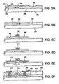
- FIGS. 5A-5F show a manufacturing method of a thin film transistor for a pixel region in accordance with Example 2 of the present invention
- FIGS. 6A-6F show a manufacturing method of a thin film transistor for a pixel region in accordance with Example 3 of the present invention
- FIGS. 7A-7F show a manufacturing method of a thin film transistor for a peripheral circuit in accordance with Example 3 of the present invention.
- FIG. 8 shows a block diagram of an active matrix type liquid crystal device in accordance with Example 4 of the present invention.
- FIG. 1 shows a schematic diagram of a circuit substrate of an active matrix type liquid crystal device in accordance with the present invention.
- peripheral circuit regions (A) and (B) there are peripheral circuit regions (A) and (B), redundant peripheral circuit regions (A′) and (B′) which are used in case where the circuits (A) and (B) are defective.
- a pixel region having a plurality of pixel TFTs arranged in a matrix form on the same substrate for switching a plurality of pixel electrodes.
- a catalyst for promoting the crystallization of a semiconductor film is introduced by a method in which a liquid carrying the catalyst therein is used as explained below.
- a polar solvent selected from the group consisting of water, alcohol, acid and ammonium.
- nickel compounds which can be dissolved in a polar solvent are nickel bromide, nickel acetate, nickel oxalate, nickel carbonate, nickel chloride, nickel iodide, nickel nitrate, nickel sulfate, nickel formate, nickel acetylacetonate, 4-cyclohexyl butyric acid, nickel oxide and nickel hydroxide.
- a non-polar solvent for dissolving a nickel compound, for example, benzene, toluene, xylene, carbon tetrachloride, chloroform or ether.
- nickel compounds suitable for such a solvent are nickel acetyl acetonate and 2-ethyl hexanoic acid nickel.
- a surface activation agent to a catalyst containing solution in order to improve the adhesivity of the catalyst to the surface and control the adsorption property.
- the surface activation agent may be applied directly onto the surface before coating the solution.
- nickel which is a catalyst element is completely dissolved in the solution.
- nickel may not be completely dissolved in a solution.
- a material like an emulsion in which nickel metal or nickel compound powders are uniformly dispersed.
- a solution which is for forming a silicon oxide film for example, OCD (Ohka Diffusion Source) which is supplied by Tokyo Ohka Industry.
- OCD Ohka Diffusion Source
- the foregoing solutions are initially formed on an amorphous silicon film by a Spin coating method and then dried so that a film containing a catalyst for promoting a crystallization of the silicon film is formed.
- This example relates to a manufacture of a circuit substrate of an active matrix liquid crystal device as shown in FIG. 1 in accordance with the above mentioned first aspect of the present invention.
- FIGS. 2A-2F are cross sectional views for showing a manufacturing method of a TFT in the peripheral circuit regions of FIG. 1 .
- FIGS. 3A-3F are cross sectional views for showing a manufacturing method of a TFT in the pixel region of FIG. 1 . Therefore, FIGS. 2A-2F and FIGS. 3A-3F correspond with each other and the both TFTs are formed on the same substrate. It is to be understood that each step of FIGS. 2A-2F and FIGS. 3A-3F is carried out simultaneously. For example, the step of FIG. 2A is simultaneously performed as the step of FIG. 3A . Also, the same reference number is used for showing a like element.
- the substrate 201 is cleaned by washing, following which a silicon oxide film 202 of 2000 ⁇ thick is formed as a base layer by a plasma CVD using TEOS (tetra-ethoxy-silane) and oxygen as starting materials.
- TEOS tetra-ethoxy-silane
- an amorphous silicon film 203 of an intrinsic type is formed by plasma CVD to a thickness of 500-1500 ⁇ , for example, 1000 ⁇ .
- a solution containing nickel as a catalyst for example, a nickel acetate solution is formed by coating.
- the concentration of nickel in the solution is 10 ppm.
- the thickness of the oxide film should be several tens angstroms in order that nickel can penetrate through it.
- a plasma treatment, evaporation, sputtering or CVD may be used to form a nickel film or nickel containing film instead of the above coating method.
- the silicon film 203 is crystallized by a thermal annealing at a temperature of 500-620° C., for example, 550° C., for a period of 4 hours in a nitrogen atmosphere. During the annealing, nickel diffuses into the silicon film from the surface and promotes the crystallization. The crystallization proceeds in a direction perpendicular to the substrate.
- a laser light 216 As a laser light, a KrF excimer laser (wavelength 248 nm, pulse width 20 nsec) is used with an energy density of 250 mJ/cm 2 and at 2 shots/site. It is desirable to heat the substrate by another energy source to 400° C. during the laser irradiation in order to increase the effect of the laser irradiation.
- IR light irradiation is comparable with the effect obtainable with a heat annealing at a high temperature for several minutes.
- the concentration of nickel in the silicon film after the crystallization is about 10 18 atoms/cm 3 .
- the silicon film 203 is patterned by dry etching to form active regions 208 in an island form as shown in FIGS. 2C and 3C .
- the surface of the active regions 208 is exposed to a 100 volume % water vapor at a pressure of 10 atm and at a temperature of 500-600° C., typically, 550° C. for 1 hour in order to oxidize the surface and form a silicon oxide film 209 .
- the thickness of the silicon oxide film 209 is 1000 ⁇ .
- the substrate is then exposed to an ammonium atmosphere (1 atm, 100%) at 400° C.
- an infrared light having a peak at a wavelength of 0.6-4 ⁇ m, for example, 0.8-1.4 g/m for 30-180 seconds is irradiated onto the silicon oxide film 209 to perform a nitridation. It is possible to add HCl at 0.1-10% to the atmosphere during this nitridation.
- an aluminum film containing scandium at 0.01-0.2% is formed by sputtering to a thickness of 3000-8000 ⁇ , e.g. 6000 ⁇ and then patterned into a gate electrode 210 .
- the surface of the aluminum gate electrode is anodic oxidized to form an anodic oxide layer 211 of a thickness of 2000 ⁇ .
- the anodic oxidation is carried out within an ethylene glycol solution in which a tartaric acid is contained at 1-5%.
- the thickness of the anodic oxide layer 211 will determine the thickness of the offset gate area in the later step.
- an N-type conductivity impurity (phosphorous, here) is introduced into the active layer in a self-aligning manner by ion doping method (also called as plasma doping method) in order to form impurity regions 212 and 213 .
- ion doping method also called as plasma doping method
- Phosphine (PH 3 ) is used as a dopant gas.
- the acceleration voltage is 60-90 kV, for example, 80 kV.
- the dose amount is 1 ⁇ 10 15 -8 ⁇ 10 15 cm ⁇ 2 , for example, 4 ⁇ 10 15 cm ⁇ 2 .
- the impurity regions 212 and 213 are offset from the gate electrode by a distance “x”.
- This configuration is advantageous for reducing a leak current (off current) which occurs when applying a reverse bias voltage (i.e. a negative voltage in the case of an NTFT) to the gate electrode.
- a reverse bias voltage i.e. a negative voltage in the case of an NTFT
- the offset configuration is particularly advantageous when the TFT is used for controlling a pixel of an active matrix.
- an annealing is performed with a laser irradiation.
- a laser a KrF excimer laser (wavelength: 248 nm, pulse width: 20 nsec.) or other lasers may be used.
- the conditions of the laser irradiation in the case of KrF excimer laser are: energy density is 200-400 mJ/cm 2 , for example, 250 mJ/cm 2 , a number of shots is 2-10 shots per one site, for example, 2 shots.
- the substrate is heated to 200-450° C. to enhance the effect of the irradiation.
- an interlayer insulating film 214 of silicon oxide is formed through a plasma CVD to a thickness of 6000 ⁇ . Further, a transparent polyimide film 215 is formed by spin coating to obtain a leveled surface. Then, in the pixel region, a transparent conductive film made of, for example, indium tin oxide is formed on the leveled surface and patterned into a pixel electrode 300 as shown in FIG. 3F .
- the ITO electrode will be connected to a terminal of a TFT as a pixel electrode.
- the interlayer insulating films 214 and 215 are provided with contact holes, through which electrode/wirings 217 and 218 are formed to contact the impurity regions of the TFT.
- the electrode/wirings 217 and 218 are formed of a metallic material, for example, a multi-layer of titanium nitride and aluminum. As shown in FIG. 3F , one electrode 218 of the pixel TFT is connected to the pixel electrode 300 made of ITO.
- an annealing in a hydrogen atmosphere of 1 atm is carried out at 350° C. for 30 minutes in order to complete a pixel circuit of an active matrix circuit having TFTs.
- the present example relates to the second aspect of the present invention as mentioned before. Specifically, this example is directed to a manufacture of a circuit substrate for an electro-optical device of the same type shown in FIG. 1 .
- the TFTs for both the peripheral circuit and the pixel circuit have their semiconductor layer in which crystals extend (grow) in a direction parallel with the substrate surface.
- FIGS. 4A-4F are cross sectional views for showing a manufacturing method of a TFT in peripheral circuit regions of FIG. 1 in accordance with the present example
- FIGS. 5A-5F are cross sectional views for showing a manufacturing method of a TFT in the pixel region of FIG. 1 in accordance with the present example. Therefore, FIGS. 4A-4F and FIGS. 5A-5F correspond with each other and the both TFTs are formed on the same substrate. Also, the same reference number is used for showing a like element.
- the substrate 201 is cleaned by washing, following which a silicon oxide film 202 of 2000 ⁇ thick is formed as a base layer by a plasma CVD using TEOS (tetra-ethoxy-silane) and oxygen as starting materials.
- TEOS tetra-ethoxy-silane
- an amorphous silicon film 203 of an intrinsic type is formed by plasma CVD to a thickness of 500-1500 ⁇ , for example, 1000 ⁇ .
- a silicon oxide film 225 of 500-2000 ⁇ thick, for example, 1000 ⁇ is formed by plasma CVD.
- the silicon oxide film 225 is partly etched to form an exposed region 204 of the amorphous silicon film, which is to be provided with nickel in the later step.
- a solution containing nickel as a catalyst for example, a nickel acetate solution is formed by coating.
- concentration of nickel in the solution is 100 ppm.
- the thickness of the oxide film should be several tens angstroms or less in order that nickel can penetrate through it.
- a plasma treatment, evaporation, sputtering or CVD may be used to form a nickel film or nickel containing film instead of the above coating method.
- the silicon film 203 is crystallized by thermal annealing at a temperature of 500-620° C., for example, 550° C., for 4 hours in a nitrogen atmosphere.
- the crystallization starts at the region 204 of the silicon film to which nickel is directly introduced and it proceeds to adjacent regions in a direction parallel with the substrate surface as shown by an arrow in the figure. Accordingly, there is formed a crystalline silicon film in which crystals grow parallel with the substrate below the silicon oxide film 225 .
- the length of the lateral growth region is about 25 ⁇ m. Also, the direction of the crystal growth in the lateral growth region is approximately aligned with the ⁇ 111> axis of the crystal.
- the semiconductor film only in the peripheral circuit region is irradiated with a laser light 216 in order to improve the crystallinity thereof.
- a laser light a KrF excimer laser (wavelength 248 nm, pulse width 20 nsec) is used with an energy density of 250 mJ/cm 2 and at 2 shots/site. It is desirable to heat the substrate by another energy source to 400° C. during the laser irradiation in order to increase the effect of the laser irradiation.
- laser may be used instead of an excimer laser.
- an intense light instead of laser.
- an infrared light of a wavelength of 1.2 ⁇ m may be used.
- the silicon oxide film 205 is removed by etching.
- the thin oxide film formed on the region 204 is also removed.
- the silicon film 203 is patterned by dry etching in order to form active regions 208 in the form of islands.
- the region 204 was directly introduced with nickel so that the concentration of the nickel in this region is higher.
- the end portion 227 of crystal growth contains nickel at a higher concentration.
- the region 204 contains nickel at a lower concentration than the regions 204 and 227 . Accordingly, the patterning of the silicon film is performed in such a manner that the silicon island 208 (active region) does not overlap with the high concentration regions 204 or 227 .
- the surface of the active regions 208 is exposed to a 100 volume % water vapor at a pressure of 10 atm and at a temperature of 500-600° C., typically, 550° C. for 1 hour in order to oxidize the surface and form a silicon oxide film 209 as shown in FIGS. 4C and 5C .
- the thickness of the silicon oxide film 209 is 1000 ⁇ .
- the substrate is exposed to an ammonium atmosphere (1 atm, 100%) at 400° C. At this condition, an infrared light having a peak at a wavelength of 0.6-4 ⁇ m, for example, 0.8-1.4 ⁇ m for 30-180 seconds is irradiated onto the silicon oxide film 209 to perform a nitridation.
- HCl may be added at 0.1-10% to the atmosphere during this nitridation.
- an aluminum film containing scandium at 0.01-0.2% is formed by sputtering to a thickness of 3000-8000 ⁇ , for example, 6000 ⁇ and then patterned into a gate electrode 210 .
- the surface of the aluminum gate electrode is anodic oxidized to form an anodic oxide layer 211 of a thickness of 2000 ⁇ .
- the anodic oxidation is carried out within an ethylene glycol solution in which a tartaric acid is contained at 1-5%.
- the thickness of the anodic oxide layer 211 will determine the thickness of the offset gate area in the subsequent impurity introducing step by ion doping.
- an N-type conductivity impurity (phosphorous, here) is introduced into the active layer in a self-aligning manner by ion doping method (also called as plasma doping method) in order to form impurity regions 212 and 213 as source and drain regions.
- ion doping method also called as plasma doping method
- Phosphine (PH 3 ) is used as a dopant gas.
- the acceleration voltage is 60-90 kV, for example, 80 kV.
- the dose amount is 1 ⁇ 10 15 -8 ⁇ 10 15 cm ⁇ 2 , for example, 4 ⁇ 10 15 cm ⁇ 2 .
- the impurity regions 212 and 213 are offset from the gate electrode by a distance “x”.
- This configuration is advantageous for reducing a leak current (off current) which occurs when applying a reverse bias voltage (i.e. a negative voltage in the case of an NTFT) to the gate electrode.
- a reverse bias voltage i.e. a negative voltage in the case of an NTFT
- the offset configuration is particularly advantageous when the TFT is used for controlling a pixel of an active matrix.
- an annealing is performed with a laser irradiation.
- a laser a KrF excimer laser (wavelength: 248 nm, pulse width: 20 nsec.) or other lasers may be used.
- the conditions of the laser irradiation in the case of KrF excimer laser are: energy density is 200-400 mJ/cm 2 , for example, 250 mJ/cm 2 , a number of shots is 2-10 shots per one site, for example, 2 shots.
- the substrate is heated to 200-450° C. to enhance the effect of the irradiation.
- an interlayer insulating film 214 of silicon oxide is formed through a plasma CVD to a thickness of 6000 ⁇ . Further, a transparent polyimide film 215 is formed by spin coating to obtain a leveled surface. Then, a transparent conductive film made of, for example, indium tin oxide is formed on the leveled surface and patterned into a pixel electrode 300 as shown in FIG. 5F . The ITO electrode will be connected to a terminal of a TFT as a pixel electrode in the pixel region.
- the interlayer insulating films 214 and 215 are provided with contact holes, through which electrode/wirings 217 and 218 are formed to contact the impurity regions of the TFT.
- the electrode/wirings 217 and 218 are formed of a metallic material, for example, a multi-layer of titanium nitride and aluminum. As shown in FIG. 5F , one electrode 218 of the pixel TFT is connected to the pixel electrode 300 made of ITO.
- an annealing in a hydrogen atmosphere of 1 atm is carried out at 350° C. for 30 minutes in order to complete a pixel circuit of an active matrix circuit having TFTs.
- the TFTs of the pixel region shown in FIG. 5F in such a manner that the direction of crystal growth is approximately orthogonal to the direction of the carrier flow of the TFT.
- the TFTs of a peripheral circuit shown in FIG. 4F are arranged so that the direction of the carrier flow is aligned with the direction of the crystal growth. Accordingly, the carriers flow along grain boundaries and it is possible to increase the mobility.
- nickel should be introduced into a region of the silicon film, which is in front of the TFT or behind the TFT in the drawing sheet. By doing so, the crystals laterally grow in a direction which is perpendicular to the direction along source and drain regions 212 and 213 , resulting in that the carriers pass across grain boundaries.
- Other manufacturing conditions may be entirely the same as those explained before.
- the present example is directed to a manufacture of an active matrix liquid crystal device as shown in FIG. 1 .
- the TFTs of the pixel region are formed with a crystalline silicon film in which crystals grew in a direction perpendicular to the substrate surface while the TFTs of the peripheral circuit (also called as driver TFTs) are formed with a crystalline silicon film in which crystals grew in a direction parallel with the substrate surface. Therefore, the present example is characterized in that crystal growths of the pixel TFTs and the driver TFTs occur in different ways from each other.
- the silicon film for forming the pixel TFTs will be directly added in its hole area with a catalyst material for promoting a crystallization thereof and then thermally crystallized.
- the silicon film for forming the driver TFTs will be crystallized by introducing a catalyst into a first region and then thermally annealed in order that the crystals grow from the first region toward a second region adjacent thereto horizontally with respect to the substrate.
- the amount of the catalyst element introduced into the foregoing regions is varied in each region. This is because the crystal structure of the obtained film depends upon the amount of the catalyst element.
- the concentration of the catalyst element in the active regions can be mad almost the same because the concentration of the catalyst element in the lateral growth region is smaller than that in the region to which the catalyst element is directly introduced.
- FIGS. 6A-6F are cross sectional views for showing a manufacturing method of a TFT in the pixel region of FIG. 1 in accordance with the present example
- FIGS. 7A-7F are cross sectional views for showing a manufacturing method of a TFT in the peripheral circuit regions of FIG. 1 in accordance with the present example. Therefore, FIGS. 6A-6F and FIGS. 7A-7F correspond with each other and the both TFTs are formed on the same substrate.
- a surface of a substrate 201 is cleaned by a proper cleaning method and a silicon oxide film 202 is formed on the cleaned surface to a thickness of 2000 ⁇ by plasma CVD using TEOS and oxygen as starting gases.
- an intrinsic (i-type) amorphous silicon film 203 is formed by plasma CVD or LPCVD to a thickness of 500-1500 ⁇ , for example, 1000 ⁇ .
- a silicon oxide film 225 is formed by plasma CVD to a thickness of 500-2000 ⁇ , for example, 1000 ⁇ .
- the oxide film 225 is selectively etched in order that only the pixel region of the amorphous silicon film 203 is exposed. Therefore, the peripheral circuit region of the silicon film remains covered with the oxide film 225 which functions as a mask in the later step.
- an extremely thin oxide film (e.g. several tens A thick) is formed on the exposed surface of the amorphous silicon film 203 .
- This extremely thin oxide film improves the wetting property of the surface with respect to a solution which will be applied later.
- the oxide film may be formed by thermal oxidation, or a UV irradiation in an oxygen gas.
- an acetic acid salt solution 205 which contain nickel is applied onto the entire surface by coating in order that the exposed surfaces of the amorphous silicon film are provided with nickel.
- the volume concentration of nickel in the acetate solution is 10 ppm.
- the substrate is heat treated at 200-500° C., for example, 300° C. so that nickel silicide is formed on the surface of the amorphous silicon film which is directly provided with the acetic acid salt solution. Accordingly, only the pixel region of the silicon film is provided with the nickel silicide while the peripheral circuit region of the silicon film is not provided with nickel silicide because of the existence of the mask made of the silicon oxide film 225 .
- the silicon oxide film 225 used as a mask is removed and another silicon oxide film 225 ′ is formed on the entire surface.
- the formation of the silicon oxide film may be done in the same manner as the formation of the oxide film 225 .
- the silicon oxide film 225 ′ is patterned to expose only a portion of the silicon film as shown in FIG. 7B .
- the silicon film 203 on the pixel region is completely covered with the silicon oxide film 225 ′.
- an acetic acid salt solution 205 ′ which contains nickel as a crystallization promoting catalyst is coated onto the entire surface. Therefore, only the exposed region of the silicon film is provided with the nickel.
- the volume concentration of the nickel in the solution is 100 ppm. Accordingly, the amount of nickel added to the silicon film is 10 times as high as the amount of nickel added to the silicon film in the former step as shown in FIG. 6A .
- the substrate is heat treated at 200-500° C., for example, 300° C. in order to form nickel silicide on the exposed region 204 of the silicon film in FIG. 7B .
- the peripheral circuit region of the amorphous silicon film is provided with nickel at a concentration 10 times as high as the region of the amorphous silicon film in the pixel region.
- the silicon film 203 provided with the catalyst for promoting the crystallization thereof is then crystallized by thermal annealing in a nitrogen gas at 500-620° C. for example at 550° C. for 4 hours.
- the crystallization proceeds in a different manner in the pixel region and the peripheral circuit region. That is, in the pixel region of the silicon film as shown in FIG. 6A , the crystal growth occurs perpendicularly to the substrate because the entire surface of the silicon film is provided with nickel.
- the region 204 is selectively provided with nickel, the crystallization proceeds from the region 204 to a region 228 adjacent thereto in a lateral direction.
- the crystallization of the former type is called a vertical growth and the latter is called a lateral growth as said before.
- the length of the lateral growth is about 30 ⁇ m. This can be increased by increasing the amount of the added nickel, by elevating the temperature of the thermal annealing and/or by increasing the time of the thermal annealing. Also, it was confirmed that the lateral crystal growth direction in the region 228 is aligned with the ⁇ 111> axis of the crystal.
- the concentration of nickel in the silicon film is 1 ⁇ 10 18 atoms/cm 3 at the pixel region of FIG. 6B , and 1 ⁇ 10 19 atoms/cm 3 at the region 204 of FIG. 7B , and 1 ⁇ 10 18 atoms/cm 3 at the region 228 . Accordingly, the nickel concentration in active regions of TFTs for both of the peripheral circuit region and the pixel region is controlled to be 1 ⁇ 10 18 atoms/cm 3 .
- it is possible to control the nickel concentration by changing the amount of nickel to be added. For example, when the crystallinity of the semiconductor film in the pixel region may be lowered, the nickel concentration in the solution 205 may be lowered. Also, when it is desired to increase the crystal growth length in FIG. 7B , the nickel concentration in the acetic acid salt solution 205 ′ should be increased.
- an infrared light having a wavelength of 1.2 ⁇ m or laser light may be used as a light source. Also, it is appropriate to irradiate only the peripheral circuit region with light in the same manner as in the first example of the present invention.
- the silicon oxide film 225 ′ is removed by etching and then the silicon film 203 is patterned by dry etching in order to form active regions 300 and 301 in the form of an island.
- the active region 300 comprises the crystalline silicon in which crystals grew in a direction vertical to the substrate.
- the active region 301 comprises the crystalline silicon film in which crystals grew from the region 204 in a lateral direction.
- the region 204 was directly introduced with nickel so that the concentration of the nickel in this region is higher. Also, the region 227 which is a top end of crystal growth also contains nickel at a higher concentration. Accordingly, the patterning of the silicon film is performed in such a manner that the active region does not overlap with the high concentration regions 204 and 227 .
- a silicon oxide film 209 of 1000 ⁇ thick is formed by LPCVD as a gate insulating film.
- an aluminum film containing scandium 0.01 to 0.2% is deposited to 3000-8000 ⁇ thick, for example, 6000 ⁇ thick by sputtering, and then patterned into a gate electrode 210 . ( FIGS. 6C and 7C )
- the surface of the aluminum gate electrode is anodic oxidized to form an anodic oxide layer 211 of a thickness of 2000 ⁇ .
- the anodic oxidation is carried out within an ethylene glycol solution in which a tartaric acid is contained at 1-5%.
- the thickness of the anodic oxide layer 211 will determine the thickness of the offset gate area in the subsequent impurity introducing step by ion doping.
- an N-type conductivity impurity (phosphorous, for example) is introduced into the active layer in a self-aligning manner by ion doping method in order to form impurity regions 212 and 213 as source and drain regions.
- Phosphine (PH 3 ) is used as a dopant gas.
- the acceleration voltage is 60-90 kV, for example, 80 kV.
- the dose amount is 1 ⁇ 10 15 -8 ⁇ 10 15 cm ⁇ 2 , for example, 4 ⁇ 10 15 cm ⁇ 2 .
- the impurity regions 212 and 213 are offset from the gate electrode by a distance “x”.
- This configuration is advantageous for reducing a leak current (off current) which occurs when applying a reverse bias voltage (i.e. a negative voltage in the case of an NTFT) to the gate electrode.
- a reverse bias voltage i.e. a negative voltage in the case of an NTFT
- CMOS structure for the peripheral circuit, it is necessary to introduce a P-type impurity as a dopant.
- a mask may be used so that the ion doping can be selectively performed.
- an annealing is performed with a laser irradiation.
- a laser a KrF excimer laser (wavelength: 248 nm, pulse width: 20 nsec.) or other lasers may be used.
- the conditions of the laser irradiation in the case of KrF excimer laser are: energy density is 200-400 mJ/cm 2 , for example, 250 mJ/cm 2 , a number of shots is 2-10 shots per one site, for example, 2 shots.
- the substrate is heated to 200-450° C. to enhance the effect of the irradiation.
- an interlayer insulating film 214 of silicon oxide is formed through a plasma CVD to a thickness of 6000 ⁇ . Further, a transparent polyimide film 215 is formed by spin coating to obtain a leveled surface. Then, a transparent conductive film made of, for example, indium tin oxide is formed on the leveled surface and patterned into a pixel electrode 300 as shown in FIG. 6F .
- the interlayer insulating films 214 and 215 are provided with contact holes, through which electrode/wirings 217 and 218 are formed to contact the impurity regions of the TFT.
- the electrode/wirings 217 and 218 are formed of a metallic material, for example, a multi-layer of titanium nitride and aluminum. As shown in FIG. 6F , one electrode 218 of the pixel TFT is connected to the pixel electrode 300 made of ITO.
- an annealing in a hydrogen atmosphere of 1 atm is carried out at 350° C. for 30 minutes in order to complete the TFTs for the active matrix and the peripheral circuit of a liquid crystal device.
- the TFT shown in FIG. 6F utilizes the vertical growth silicon film so that the carriers must pass across grain boundaries. Therefore, the mobility and the ON current is relatively small because of the influence of the grain boundaries. However, the OFF current can be reduced.
- the TFT shown in FIG. 7F utilizes the lateral growth silicon film so that carriers flow in a direction approximately parallel with the crystal growth direction. Therefore, the influence of the grain boundaries can be reduced and the ON current is increased.
- an integrated circuit is to be formed on one glass substrate by mounting thereon a display, CPU, memory etc by employing the third aspect of the invention in which a desired crystalline structure or crystal structure (lateral growth or vertical growth) may be obtained in a desired region.
- FIG. 8 shows a block diagram of an electro-optical system (device).
- the input port is to read a signal input from an outside and to convert it into a display signal
- the correction memory is peculiar to each panel, which corrects the input signal or the like in accordance with a specific characteristics of an active matrix panel.
- the correction memory uses a non-volatile memory in which an information of each pixel is stored in order to perform the correction at each pixel. That is, if there is a defective pixel (point defect) in the electro-optical device, pixels surrounding the defective pixel are supplied with signals which are corrected in order to disappear or cover the defect pixel. Also, when there is a pixel of which brightness is lower than others, the signal to be applied to that pixel is corrected to be a larger signal, thereby, the brightness of that pixel becomes the same as its surrounding pixels.
- the CPU and the memory are equivalent to those used in a conventional computer.
- the memory uses a RAM in which an image memory corresponding to each pixel is stored. Also, it has a function of changing an intensity of back light on the rear side of the substrate in response to the image information.
- the reference numeral 74 shows a region on which a decoder/driver circuit which is a peripheral circuit is formed.
- 71 shows an active matrix TFT
- 72 shows a capacitor
- 73 shows a liquid crystal.
- the foregoing circuits are formed on one substrate.
- a crystalline silicon film is selectively formed depending upon the required crystallinity or crystal structure.
Abstract
A semiconductor device using a crystalline semiconductor film is manufactured. The crystalline semiconductor film is formed by providing an amorphous silicon film with a catalyst metal for promoting a crystallization thereof and then heated for performing a thermal crystallization, following which the crystallized film is further exposed to a laser light for improving the crystallinity. The concentration of the catalyst metal in the semiconductor film and the location of the region to be added with the catalyst metal are so selected in order that a desired crystallinity and a desired crystal structure such as a vertical crystal growth or lateral crystal growth can be obtained. Further, active elements and driver elements of a circuit substrate for an active matrix type liquid crystal device are formed by such semiconductor devices having a desired crystallinity and crystal structure respectively.
Description
The present invention relates to an active-matrix type liquid crystal device or thin film integrated circuit devices using a semiconductor layer with crystallinity.
Active-matrix type liquid crystal devices have been well known which utilize thin film transistors (generally called as TFT). In a conventional active-matrix liquid crystal display device, a peripheral circuit member is constituted by IC and is externally connected to terminals of matrix wirings of the pixels. Further, it is also known to form TFTs for forming a peripheral circuit on the same substrate on which TFTs are arranged in a matrix as a switching element in a pixel region.
Since the TFTs formed on a peripheral circuit portion are to drive the TFTs formed in a matrix form on a pixel portion, they are required to have a capability of passing a large amount of electric current therethrough. Specifically, they are required to have a large ON current and a large mobility.
On the other hand, the TFTs formed on the pixel portion are not required to have a large mobility. Rather, they need to have a lower OFF current (leak current) in order to maintain electric charges on pixel electrodes. Accordingly, the required characteristics for the TFTs of a peripheral circuit are different from those for the TFTs of a pixel portion.
Further, an amorphous silicon film has been used to form a TFT but its characteristics are not satisfactory. Therefore, a TFT using a crystalline silicon film has been investigated. Generally, it is necessary to perform a thermal annealing at 600° C. or higher and for more than 24 hours for obtain a crystalline silicon film from an amorphous silicon film. However, a glass substrate which is usually used as a substrate of a liquid crystal device can not endure such a thermal annealing because for example, a Corning 7059 glass has a distortion point of 593° C. In particular, one problem is that the glass substrate tends to be distorted because of the high temperature so that it is difficult to increase the size of the substrate.
The inventors of the present application have confirmed through their experiments that by contacting a slight amount of catalyst metal such as nickel or platinum with an amorphous silicon film, it is possible to crystallize the silicon film at lower temperatures, for example, at ˜550° C. for about 4 hours. And the resultant crystallinity is comparable with that obtained the above conventional thermal treatment at 600° C. The inventors considered that these metal functions as a catalyst to promote the crystallization of an amorphous silicon film.
The inventors also confirmed that there are two types of crystallization in the case of using a catalyst as indicated below.
(1) A crystallization proceeds in a direction normal to a substrate in a region where a catalyst was introduced.
(2) A crystallization proceeds in a direction parallel with a substrate from a region to which a catalyst was introduced toward a region to which a catalyst was not introduced.
The crystal structure in the case of (2) was confirmed by using a TEM (transmission type electron microscope) that columnar crystals grow in a direction parallel with a substrate. Also, the amount of nickel necessary for causing the above first type of crystallization is different from the amount of nickel necessary for causing the above second type of crystallization. For example, when the (2) type of crystallization extends about 30 μm, the amount of the nickel necessary to be introduced thereto is 10 times as much as that required in the case of (1).
In the present specification, hereinbelow, the region where the above (1) type of crystallization occurs will be called as a vertical growth region and the region where the above (2) type of crystallization occurs will be called as a lateral growth region.
It is an object of the present invention to form thin film transistors on a pixel region (pixel TFTs) and thin film transistors on a peripheral circuit region on a same substrate through a simple process for an active-matrix type liquid crystal device.
Moreover, it is another object of the present invention that, in an active-matrix type liquid crystal device, pixel TFTs have a different crystallinity than TFTs formed on a peripheral circuit region.
In accordance with one aspect of the present invention, the method of the present invention includes a step of irradiating a laser light or a light having a sufficient strength on a selected portion of a semiconductor film to constitute a peripheral circuit region.
In accordance with another aspect of the invention, TFTs constituting a peripheral circuit are formed with a crystalline silicon film in which crystals grew in a direction approximately parallel with a direction along which carriers of the TFTs flow while pixel TFTs are formed with a crystalline silicon film in which crystals grew in a direction approximately perpendicularly with respect to a carrier direction of the pixel TFTs. The carrier direction means the direction along source and drain regions of the TFT. Namely, when a carrier direction is approximately aligned with a crystal growth direction, since carriers move along the direction of grain boundaries, the influence of the grain boundaries with respect to the carrier flow is suppressed and thus such a TFT can have a higher mobility. Accordingly, such a TFT is suitable for forming a peripheral circuit which requires a higher ON current. On the other hand, when a carrier direction is perpendicular to a crystal growth direction, since carriers have to cross grain boundaries, the OFF current can be decreased while the ON current is decreased. Accordingly, such a TFT is suitable as a pixel TFT for switching a pixel electrode in an electro-optical device.
It is still a further aspect of the present invention that TFTs having a channel region formed with a vertical growth silicon film (i.e. in which crystals grew perpendicularly to the substrate) and TFTs having a channel region formed with a lateral growth silicon (i.e. in which crystals grew horizontally with the substrate) are both formed on the same substrate. Specifically, the TFTs associated with the vertical growth region is suitable as pixel TFTs for switching pixel electrodes while the TFTs associated with the lateral growth region is suitable as a peripheral circuit for driving the pixel TFTs. This feature is based on the inventors' discovery that the amount of a catalyst required for forming a vertical growth film and that for forming a lateral growth film are different from each other. In order to accurately control the amount of a catalyst to be introduced into a semiconductor film, the inventors utilize a liquid for carrying a catalyst therein.
In accordance with the present invention the catalyst may be one or more elements selected from the group consisting of Ni, Pd, Pt, Cu, Ag, Au, In, Sn, P, As and Sb. Alternatively, the catalyst may be one or more elements selected from the group consisting of Group VIII elements, Group IIIb elements, Group IVb elements and Group Vb elements.
The foregoing and other objects and features of the present invention will be explained in detail with reference to the attached drawings in which:
In FIG. 1 , on a substrate 201, there are peripheral circuit regions (A) and (B), redundant peripheral circuit regions (A′) and (B′) which are used in case where the circuits (A) and (B) are defective. There is also a pixel region having a plurality of pixel TFTs arranged in a matrix form on the same substrate for switching a plurality of pixel electrodes.
In accordance with the preferred embodiments of the invention, a catalyst for promoting the crystallization of a semiconductor film is introduced by a method in which a liquid carrying the catalyst therein is used as explained below.
For preparing a liquid carrying the catalyst, it is possible to use a polar solvent selected from the group consisting of water, alcohol, acid and ammonium. Examples of nickel compounds which can be dissolved in a polar solvent are nickel bromide, nickel acetate, nickel oxalate, nickel carbonate, nickel chloride, nickel iodide, nickel nitrate, nickel sulfate, nickel formate, nickel acetylacetonate, 4-cyclohexyl butyric acid, nickel oxide and nickel hydroxide.
Also, it is possible to use a non-polar solvent for dissolving a nickel compound, for example, benzene, toluene, xylene, carbon tetrachloride, chloroform or ether. Examples of nickel compounds suitable for such a solvent are nickel acetyl acetonate and 2-ethyl hexanoic acid nickel.
Also, it is advantageous to add a surface activation agent to a catalyst containing solution in order to improve the adhesivity of the catalyst to the surface and control the adsorption property. The surface activation agent may be applied directly onto the surface before coating the solution.
In the above mentioned solutions, nickel which is a catalyst element is completely dissolved in the solution. However, it is to be understood that nickel may not be completely dissolved in a solution. For example, it is possible to use a material like an emulsion in which nickel metal or nickel compound powders are uniformly dispersed. It is also possible to use a solution which is for forming a silicon oxide film, for example, OCD (Ohka Diffusion Source) which is supplied by Tokyo Ohka Industry. In such a case, it is possible to form a silicon oxide film which contains a catalyst therein by simply coating the solution and then baking at 200° C. Desired impurities can be also added to the solution.
The foregoing solutions are initially formed on an amorphous silicon film by a Spin coating method and then dried so that a film containing a catalyst for promoting a crystallization of the silicon film is formed.
This example relates to a manufacture of a circuit substrate of an active matrix liquid crystal device as shown in FIG. 1 in accordance with the above mentioned first aspect of the present invention.
Initially, referring to FIGS. 2A and 3A , the substrate 201 is cleaned by washing, following which a silicon oxide film 202 of 2000 Å thick is formed as a base layer by a plasma CVD using TEOS (tetra-ethoxy-silane) and oxygen as starting materials.
Then, an amorphous silicon film 203 of an intrinsic type is formed by plasma CVD to a thickness of 500-1500 Å, for example, 1000 Å. On the amorphous silicon film 203, a solution containing nickel as a catalyst, for example, a nickel acetate solution is formed by coating. The concentration of nickel in the solution is 10 ppm. Also, it is advantageous to form a very thin oxide film on the amorphous silicon film before the formation of the nickel containing solution in order to improve the wettability of the surface. The thickness of the oxide film should be several tens angstroms in order that nickel can penetrate through it.
It should be noted that a plasma treatment, evaporation, sputtering or CVD may be used to form a nickel film or nickel containing film instead of the above coating method.
After drying the coated solution 205, the silicon film 203 is crystallized by a thermal annealing at a temperature of 500-620° C., for example, 550° C., for a period of 4 hours in a nitrogen atmosphere. During the annealing, nickel diffuses into the silicon film from the surface and promotes the crystallization. The crystallization proceeds in a direction perpendicular to the substrate.
Referring to FIG. 2B , after the above crystallization, only the region of the semiconductor film which corresponds to the peripheral circuit region is irradiated with a laser light 216 in order to improve the crystallinity. As a laser light, a KrF excimer laser (wavelength 248 nm, pulse width 20 nsec) is used with an energy density of 250 mJ/cm2 and at 2 shots/site. It is desirable to heat the substrate by another energy source to 400° C. during the laser irradiation in order to increase the effect of the laser irradiation.
Also, other known lasers may be used instead of the excimer laser. Moreover, it is also possible to use an intense light instead of laser. For example, an infrared light of a wavelength of 1.2 μm may be used. The effect of the IR light irradiation is comparable with the effect obtainable with a heat annealing at a high temperature for several minutes.
The concentration of nickel in the silicon film after the crystallization is about 1018 atoms/cm3. Then, the silicon film 203 is patterned by dry etching to form active regions 208 in an island form as shown in FIGS. 2C and 3C .
Thereafter, the surface of the active regions 208 is exposed to a 100 volume % water vapor at a pressure of 10 atm and at a temperature of 500-600° C., typically, 550° C. for 1 hour in order to oxidize the surface and form a silicon oxide film 209. The thickness of the silicon oxide film 209 is 1000 Å. After the oxidation, the substrate is then exposed to an ammonium atmosphere (1 atm, 100%) at 400° C. At this condition, an infrared light having a peak at a wavelength of 0.6-4 μm, for example, 0.8-1.4 g/m for 30-180 seconds is irradiated onto the silicon oxide film 209 to perform a nitridation. It is possible to add HCl at 0.1-10% to the atmosphere during this nitridation.
Subsequently, an aluminum film containing scandium at 0.01-0.2% is formed by sputtering to a thickness of 3000-8000 Å, e.g. 6000 Å and then patterned into a gate electrode 210.
Then, referring to FIGS. 2D and 3D , the surface of the aluminum gate electrode is anodic oxidized to form an anodic oxide layer 211 of a thickness of 2000 Å. The anodic oxidation is carried out within an ethylene glycol solution in which a tartaric acid is contained at 1-5%. The thickness of the anodic oxide layer 211 will determine the thickness of the offset gate area in the later step.
Referring then to FIGS. 2E and 3E , using the gate electrode 210 and the surrounding anodic oxide film 211 as a mask, an N-type conductivity impurity (phosphorous, here) is introduced into the active layer in a self-aligning manner by ion doping method (also called as plasma doping method) in order to form impurity regions 212 and 213. Phosphine (PH3) is used as a dopant gas. The acceleration voltage is 60-90 kV, for example, 80 kV. The dose amount is 1×10¹⁵-8×1015 cm−2, for example, 4×1015 cm−2. As can be seen in the drawing, the impurity regions 212 and 213 are offset from the gate electrode by a distance “x”. This configuration is advantageous for reducing a leak current (off current) which occurs when applying a reverse bias voltage (i.e. a negative voltage in the case of an NTFT) to the gate electrode. In particular, since it is desired that electric charges stored in a pixel electrode be maintained without leaking in order to obtain an excellent display, the offset configuration is particularly advantageous when the TFT is used for controlling a pixel of an active matrix.
Thereafter, an annealing is performed with a laser irradiation. As a laser, a KrF excimer laser (wavelength: 248 nm, pulse width: 20 nsec.) or other lasers may be used. The conditions of the laser irradiation in the case of KrF excimer laser are: energy density is 200-400 mJ/cm2, for example, 250 mJ/cm2, a number of shots is 2-10 shots per one site, for example, 2 shots. Preferably, the substrate is heated to 200-450° C. to enhance the effect of the irradiation.
Referring to FIGS. 2F and 3F , an interlayer insulating film 214 of silicon oxide is formed through a plasma CVD to a thickness of 6000 Å. Further, a transparent polyimide film 215 is formed by spin coating to obtain a leveled surface. Then, in the pixel region, a transparent conductive film made of, for example, indium tin oxide is formed on the leveled surface and patterned into a pixel electrode 300 as shown in FIG. 3F . The ITO electrode will be connected to a terminal of a TFT as a pixel electrode.
Then, the interlayer insulating films 214 and 215 are provided with contact holes, through which electrode/ wirings 217 and 218 are formed to contact the impurity regions of the TFT. The electrode/ wirings 217 and 218 are formed of a metallic material, for example, a multi-layer of titanium nitride and aluminum. As shown in FIG. 3F , one electrode 218 of the pixel TFT is connected to the pixel electrode 300 made of ITO.
Finally, an annealing in a hydrogen atmosphere of 1 atm is carried out at 350° C. for 30 minutes in order to complete a pixel circuit of an active matrix circuit having TFTs.
The present example relates to the second aspect of the present invention as mentioned before. Specifically, this example is directed to a manufacture of a circuit substrate for an electro-optical device of the same type shown in FIG. 1 . In particular, the TFTs for both the peripheral circuit and the pixel circuit have their semiconductor layer in which crystals extend (grow) in a direction parallel with the substrate surface.
Initially, referring to FIGS. 4A and 5A , the substrate 201 is cleaned by washing, following which a silicon oxide film 202 of 2000 Å thick is formed as a base layer by a plasma CVD using TEOS (tetra-ethoxy-silane) and oxygen as starting materials.
Then, an amorphous silicon film 203 of an intrinsic type is formed by plasma CVD to a thickness of 500-1500 Å, for example, 1000 Å. Subsequently, a silicon oxide film 225 of 500-2000 Å thick, for example, 1000 Å is formed by plasma CVD. Then, the silicon oxide film 225 is partly etched to form an exposed region 204 of the amorphous silicon film, which is to be provided with nickel in the later step.
Then, a solution containing nickel as a catalyst, for example, a nickel acetate solution is formed by coating. The concentration of nickel in the solution is 100 ppm. Also, it is advantageous to form a very thin oxide film on the amorphous silicon film before the formation of the nickel containing solution in order to improve the wettability of the surface. The thickness of the oxide film should be several tens angstroms or less in order that nickel can penetrate through it.
It should be noted that a plasma treatment, evaporation, sputtering or CVD may be used to form a nickel film or nickel containing film instead of the above coating method.
After drying the coated solution 205, the silicon film 203 is crystallized by thermal annealing at a temperature of 500-620° C., for example, 550° C., for 4 hours in a nitrogen atmosphere. The crystallization starts at the region 204 of the silicon film to which nickel is directly introduced and it proceeds to adjacent regions in a direction parallel with the substrate surface as shown by an arrow in the figure. Accordingly, there is formed a crystalline silicon film in which crystals grow parallel with the substrate below the silicon oxide film 225. The length of the lateral growth region is about 25 μm. Also, the direction of the crystal growth in the lateral growth region is approximately aligned with the <111> axis of the crystal.
Referring to FIG. 4B , after the above crystallization, the semiconductor film only in the peripheral circuit region is irradiated with a laser light 216 in order to improve the crystallinity thereof. As a laser light, a KrF excimer laser (wavelength 248 nm, pulse width 20 nsec) is used with an energy density of 250 mJ/cm2 and at 2 shots/site. It is desirable to heat the substrate by another energy source to 400° C. during the laser irradiation in order to increase the effect of the laser irradiation.
Also, another kind of laser may be used instead of an excimer laser. Moreover, it is possible to use an intense light instead of laser. For example, an infrared light of a wavelength of 1.2 μm may be used.
Then, the silicon oxide film 205 is removed by etching. At the same time, the thin oxide film formed on the region 204 is also removed. Further, the silicon film 203 is patterned by dry etching in order to form active regions 208 in the form of islands. The region 204 was directly introduced with nickel so that the concentration of the nickel in this region is higher. Also, the end portion 227 of crystal growth contains nickel at a higher concentration. On the other hand, the region 204 contains nickel at a lower concentration than the regions 204 and 227. Accordingly, the patterning of the silicon film is performed in such a manner that the silicon island 208 (active region) does not overlap with the high concentration regions 204 or 227.
Thereafter, the surface of the active regions 208 is exposed to a 100 volume % water vapor at a pressure of 10 atm and at a temperature of 500-600° C., typically, 550° C. for 1 hour in order to oxidize the surface and form a silicon oxide film 209 as shown in FIGS. 4C and 5C . The thickness of the silicon oxide film 209 is 1000 Å. After the oxidation, the substrate is exposed to an ammonium atmosphere (1 atm, 100%) at 400° C. At this condition, an infrared light having a peak at a wavelength of 0.6-4 μm, for example, 0.8-1.4 μm for 30-180 seconds is irradiated onto the silicon oxide film 209 to perform a nitridation. HCl may be added at 0.1-10% to the atmosphere during this nitridation.
Subsequently, an aluminum film containing scandium at 0.01-0.2% is formed by sputtering to a thickness of 3000-8000 Å, for example, 6000 Å and then patterned into a gate electrode 210.
Then, referring to FIGS. 4D and 5D , the surface of the aluminum gate electrode is anodic oxidized to form an anodic oxide layer 211 of a thickness of 2000 Å. The anodic oxidation is carried out within an ethylene glycol solution in which a tartaric acid is contained at 1-5%. The thickness of the anodic oxide layer 211 will determine the thickness of the offset gate area in the subsequent impurity introducing step by ion doping.
Referring then to FIGS. 4E and 5E , using the gate electrode 210 and the surrounding anodic oxide film 211 as a mask, an N-type conductivity impurity (phosphorous, here) is introduced into the active layer in a self-aligning manner by ion doping method (also called as plasma doping method) in order to form impurity regions 212 and 213 as source and drain regions. Phosphine (PH3) is used as a dopant gas. The acceleration voltage is 60-90 kV, for example, 80 kV. The dose amount is 1×10¹⁵-8×1015 cm−2, for example, 4×1015 cm−2. As can be seen in the drawing, the impurity regions 212 and 213 are offset from the gate electrode by a distance “x”. This configuration is advantageous for reducing a leak current (off current) which occurs when applying a reverse bias voltage (i.e. a negative voltage in the case of an NTFT) to the gate electrode. In particular, since it is desired that electric charges stored in a pixel electrode be maintained without leaking in order to obtain an excellent display, the offset configuration is particularly advantageous when the TFT is used for controlling a pixel of an active matrix.
Thereafter, an annealing is performed with a laser irradiation. As a laser, a KrF excimer laser (wavelength: 248 nm, pulse width: 20 nsec.) or other lasers may be used. The conditions of the laser irradiation in the case of KrF excimer laser are: energy density is 200-400 mJ/cm2, for example, 250 mJ/cm2, a number of shots is 2-10 shots per one site, for example, 2 shots. Preferably, the substrate is heated to 200-450° C. to enhance the effect of the irradiation.
Referring to FIGS. 4F and 5F , an interlayer insulating film 214 of silicon oxide is formed through a plasma CVD to a thickness of 6000 Å. Further, a transparent polyimide film 215 is formed by spin coating to obtain a leveled surface. Then, a transparent conductive film made of, for example, indium tin oxide is formed on the leveled surface and patterned into a pixel electrode 300 as shown in FIG. 5F . The ITO electrode will be connected to a terminal of a TFT as a pixel electrode in the pixel region.
Then, the interlayer insulating films 214 and 215 are provided with contact holes, through which electrode/ wirings 217 and 218 are formed to contact the impurity regions of the TFT. The electrode/ wirings 217 and 218 are formed of a metallic material, for example, a multi-layer of titanium nitride and aluminum. As shown in FIG. 5F , one electrode 218 of the pixel TFT is connected to the pixel electrode 300 made of ITO.
Finally, an annealing in a hydrogen atmosphere of 1 atm is carried out at 350° C. for 30 minutes in order to complete a pixel circuit of an active matrix circuit having TFTs.
As a modification of the second example, it is advantageous to arrange the TFTs of the pixel region shown in FIG. 5F in such a manner that the direction of crystal growth is approximately orthogonal to the direction of the carrier flow of the TFT. Thereby, it is possible to minimize an OFF 10 current when the TFT is in its OFF condition because the carriers must pass across grain boundaries. On the other hand, the TFTs of a peripheral circuit shown in FIG. 4F are arranged so that the direction of the carrier flow is aligned with the direction of the crystal growth. Accordingly, the carriers flow along grain boundaries and it is possible to increase the mobility. In order to achieve such a configuration, during the manufacture of the pixel TFTs shown in FIGS. 5A-5F , nickel should be introduced into a region of the silicon film, which is in front of the TFT or behind the TFT in the drawing sheet. By doing so, the crystals laterally grow in a direction which is perpendicular to the direction along source and drain regions 212 and 213, resulting in that the carriers pass across grain boundaries. Other manufacturing conditions may be entirely the same as those explained before.
The present example is directed to a manufacture of an active matrix liquid crystal device as shown in FIG. 1 . In the device of the present example, the TFTs of the pixel region are formed with a crystalline silicon film in which crystals grew in a direction perpendicular to the substrate surface while the TFTs of the peripheral circuit (also called as driver TFTs) are formed with a crystalline silicon film in which crystals grew in a direction parallel with the substrate surface. Therefore, the present example is characterized in that crystal growths of the pixel TFTs and the driver TFTs occur in different ways from each other.
The silicon film for forming the pixel TFTs will be directly added in its hole area with a catalyst material for promoting a crystallization thereof and then thermally crystallized.
Also, the silicon film for forming the driver TFTs will be crystallized by introducing a catalyst into a first region and then thermally annealed in order that the crystals grow from the first region toward a second region adjacent thereto horizontally with respect to the substrate.
In accordance with the present example, the amount of the catalyst element introduced into the foregoing regions is varied in each region. This is because the crystal structure of the obtained film depends upon the amount of the catalyst element. However, the concentration of the catalyst element in the active regions can be mad almost the same because the concentration of the catalyst element in the lateral growth region is smaller than that in the region to which the catalyst element is directly introduced.
Referring to FIGS. 6A and 7A , a surface of a substrate 201 is cleaned by a proper cleaning method and a silicon oxide film 202 is formed on the cleaned surface to a thickness of 2000 Å by plasma CVD using TEOS and oxygen as starting gases. Then, an intrinsic (i-type) amorphous silicon film 203 is formed by plasma CVD or LPCVD to a thickness of 500-1500 Å, for example, 1000 Å. Subsequently, a silicon oxide film 225 is formed by plasma CVD to a thickness of 500-2000 Å, for example, 1000 Å. The oxide film 225 is selectively etched in order that only the pixel region of the amorphous silicon film 203 is exposed. Therefore, the peripheral circuit region of the silicon film remains covered with the oxide film 225 which functions as a mask in the later step.
Then, an extremely thin oxide film (e.g. several tens A thick) is formed on the exposed surface of the amorphous silicon film 203. This extremely thin oxide film improves the wetting property of the surface with respect to a solution which will be applied later. The oxide film may be formed by thermal oxidation, or a UV irradiation in an oxygen gas.
Thereafter, an acetic acid salt solution 205 which contain nickel is applied onto the entire surface by coating in order that the exposed surfaces of the amorphous silicon film are provided with nickel. The volume concentration of nickel in the acetate solution is 10 ppm.
After the coating, the substrate is heat treated at 200-500° C., for example, 300° C. so that nickel silicide is formed on the surface of the amorphous silicon film which is directly provided with the acetic acid salt solution. Accordingly, only the pixel region of the silicon film is provided with the nickel silicide while the peripheral circuit region of the silicon film is not provided with nickel silicide because of the existence of the mask made of the silicon oxide film 225.
Then, referring to FIG. 7B , the silicon oxide film 225 used as a mask is removed and another silicon oxide film 225′ is formed on the entire surface. The formation of the silicon oxide film may be done in the same manner as the formation of the oxide film 225. The silicon oxide film 225′ is patterned to expose only a portion of the silicon film as shown in FIG. 7B . On the other hand, the silicon film 203 on the pixel region is completely covered with the silicon oxide film 225′.
In the above condition, an acetic acid salt solution 205′ which contains nickel as a crystallization promoting catalyst is coated onto the entire surface. Therefore, only the exposed region of the silicon film is provided with the nickel. The volume concentration of the nickel in the solution is 100 ppm. Accordingly, the amount of nickel added to the silicon film is 10 times as high as the amount of nickel added to the silicon film in the former step as shown in FIG. 6A .
Thereafter, the substrate is heat treated at 200-500° C., for example, 300° C. in order to form nickel silicide on the exposed region 204 of the silicon film in FIG. 7B .
By the foregoing steps, the peripheral circuit region of the amorphous silicon film is provided with nickel at a concentration 10 times as high as the region of the amorphous silicon film in the pixel region.
The silicon film 203 provided with the catalyst for promoting the crystallization thereof is then crystallized by thermal annealing in a nitrogen gas at 500-620° C. for example at 550° C. for 4 hours. The crystallization proceeds in a different manner in the pixel region and the peripheral circuit region. That is, in the pixel region of the silicon film as shown in FIG. 6A , the crystal growth occurs perpendicularly to the substrate because the entire surface of the silicon film is provided with nickel. On the other hand, in the peripheral circuit region as shown in FIG. 7B , since the region 204 is selectively provided with nickel, the crystallization proceeds from the region 204 to a region 228 adjacent thereto in a lateral direction. The crystallization of the former type is called a vertical growth and the latter is called a lateral growth as said before.
The length of the lateral growth is about 30 μm. This can be increased by increasing the amount of the added nickel, by elevating the temperature of the thermal annealing and/or by increasing the time of the thermal annealing. Also, it was confirmed that the lateral crystal growth direction in the region 228 is aligned with the <111> axis of the crystal.
The concentration of nickel in the silicon film is 1×10¹⁸ atoms/cm3 at the pixel region of FIG. 6B , and 1×10¹⁹ atoms/cm3 at the region 204 of FIG. 7B , and 1×10¹⁸ atoms/cm3 at the region 228. Accordingly, the nickel concentration in active regions of TFTs for both of the peripheral circuit region and the pixel region is controlled to be 1×10¹⁸ atoms/cm3. Of course, it is possible to control the nickel concentration by changing the amount of nickel to be added. For example, when the crystallinity of the semiconductor film in the pixel region may be lowered, the nickel concentration in the solution 205 may be lowered. Also, when it is desired to increase the crystal growth length in FIG. 7B , the nickel concentration in the acetic acid salt solution 205′ should be increased.
It is desirable to irradiate the semiconductor film with intense light for improving the crystallinity after the above crystallization. An infrared light having a wavelength of 1.2 μm or laser light may be used as a light source. Also, it is appropriate to irradiate only the peripheral circuit region with light in the same manner as in the first example of the present invention.
After the crystallization step, the silicon oxide film 225′ is removed by etching and then the silicon film 203 is patterned by dry etching in order to form active regions 300 and 301 in the form of an island. In FIG. 6C , the active region 300 comprises the crystalline silicon in which crystals grew in a direction vertical to the substrate. Also, in FIG. 7C , the active region 301 comprises the crystalline silicon film in which crystals grew from the region 204 in a lateral direction.
The region 204 was directly introduced with nickel so that the concentration of the nickel in this region is higher. Also, the region 227 which is a top end of crystal growth also contains nickel at a higher concentration. Accordingly, the patterning of the silicon film is performed in such a manner that the active region does not overlap with the high concentration regions 204 and 227.
After the patterning, a silicon oxide film 209 of 1000 Å thick is formed by LPCVD as a gate insulating film. Subsequently, an aluminum film containing scandium 0.01 to 0.2% is deposited to 3000-8000 Å thick, for example, 6000 Å thick by sputtering, and then patterned into a gate electrode 210. (FIGS. 6C and 7C )
Then, referring to FIGS. 6D and 7D , the surface of the aluminum gate electrode is anodic oxidized to form an anodic oxide layer 211 of a thickness of 2000 Å. The anodic oxidation is carried out within an ethylene glycol solution in which a tartaric acid is contained at 1-5%. The thickness of the anodic oxide layer 211 will determine the thickness of the offset gate area in the subsequent impurity introducing step by ion doping.
Referring then to FIGS. 6E and 7E , using the gate electrode 210 and the surrounding anodic oxide film 211 as a mask, an N-type conductivity impurity (phosphorous, for example) is introduced into the active layer in a self-aligning manner by ion doping method in order to form impurity regions 212 and 213 as source and drain regions. Phosphine (PH3) is used as a dopant gas. The acceleration voltage is 60-90 kV, for example, 80 kV. The dose amount is 1×10¹⁵-8×1015 cm−2, for example, 4×1015 cm−2. As can be seen in the drawing, the impurity regions 212 and 213 are offset from the gate electrode by a distance “x”. This configuration is advantageous for reducing a leak current (off current) which occurs when applying a reverse bias voltage (i.e. a negative voltage in the case of an NTFT) to the gate electrode. In particular, it is advantageous to provide an offset region in the TFT for the pixel region in order to prevent charges applied to a pixel electrode from leaking.
Also, when forming a CMOS structure for the peripheral circuit, it is necessary to introduce a P-type impurity as a dopant. In such a case, a mask may be used so that the ion doping can be selectively performed.
Thereafter, an annealing is performed with a laser irradiation. As a laser, a KrF excimer laser (wavelength: 248 nm, pulse width: 20 nsec.) or other lasers may be used. The conditions of the laser irradiation in the case of KrF excimer laser are: energy density is 200-400 mJ/cm2, for example, 250 mJ/cm2, a number of shots is 2-10 shots per one site, for example, 2 shots. Preferably, the substrate is heated to 200-450° C. to enhance the effect of the irradiation.
Referring to FIGS. 6F and 7F , an interlayer insulating film 214 of silicon oxide is formed through a plasma CVD to a thickness of 6000 Å. Further, a transparent polyimide film 215 is formed by spin coating to obtain a leveled surface. Then, a transparent conductive film made of, for example, indium tin oxide is formed on the leveled surface and patterned into a pixel electrode 300 as shown in FIG. 6F .
Then, the interlayer insulating films 214 and 215 are provided with contact holes, through which electrode/ wirings 217 and 218 are formed to contact the impurity regions of the TFT. The electrode/ wirings 217 and 218 are formed of a metallic material, for example, a multi-layer of titanium nitride and aluminum. As shown in FIG. 6F , one electrode 218 of the pixel TFT is connected to the pixel electrode 300 made of ITO.
Finally, an annealing in a hydrogen atmosphere of 1 atm is carried out at 350° C. for 30 minutes in order to complete the TFTs for the active matrix and the peripheral circuit of a liquid crystal device.
The TFT shown in FIG. 6F utilizes the vertical growth silicon film so that the carriers must pass across grain boundaries. Therefore, the mobility and the ON current is relatively small because of the influence of the grain boundaries. However, the OFF current can be reduced.
Also, the TFT shown in FIG. 7F utilizes the lateral growth silicon film so that carriers flow in a direction approximately parallel with the crystal growth direction. Therefore, the influence of the grain boundaries can be reduced and the ON current is increased.
In this example, an integrated circuit is to be formed on one glass substrate by mounting thereon a display, CPU, memory etc by employing the third aspect of the invention in which a desired crystalline structure or crystal structure (lateral growth or vertical growth) may be obtained in a desired region.
The CPU and the memory are equivalent to those used in a conventional computer. Especially, the memory uses a RAM in which an image memory corresponding to each pixel is stored. Also, it has a function of changing an intensity of back light on the rear side of the substrate in response to the image information.
The reference numeral 74 shows a region on which a decoder/driver circuit which is a peripheral circuit is formed. 71 shows an active matrix TFT, 72 shows a capacitor, and 73 shows a liquid crystal. In this example, the foregoing circuits are formed on one substrate. And, a crystalline silicon film is selectively formed depending upon the required crystallinity or crystal structure.
While various examples have been disclosed, it is to be understood that the scope of the present invention should not be limited to those particular examples. Many modifications may be made without departing the scope of the invention. For example, while thin film transistors are mainly discussed, it is possible to form other types of a semiconductor device in accordance with the present invention, for example, a diode, photoelectric conversion device, etc. Also, the present invention is effective for the use of other catalyst materials in place of nickel. Furthermore, the catalyst may be first formed over a substrate and then a semiconductor film may be formed thereon.
Claims (35)
1. A method of manufacturing a semiconductor device comprising the steps of:
forming an amorphous semiconductor film over a substrate in first and second regions;
providing the amorphous semiconductor film in the first region and a part of the amorphous semiconductor film in the second region with a metal containing material;
crystallizing the semiconductor film in the first and second regions by heating;
patterning the crystallized semiconductor film to respectively form first and second semiconductor islands in the first and second regions;
forming insulating films over the first and second semiconductor islands; and
forming gate electrodes over the first and second semiconductor islands with, respectively, the insulating films interposed therebetween,
wherein the semiconductor device comprises a matrix circuit, and
wherein the matrix circuit comprises capacitors for storing charges.
2. The method according to claim 1 , wherein the metal containing material comprises a metal selected from the group consisting of Ni, Pd, Pt, Cu, Ag, Au, In, Sn, P, As and Sb.
3. The method according to claim 1 , further comprising a step of adding an impurity into the first and second semiconductor islands to for impurity regions with a channel region therebetween in the first and second semiconductor islands.
4. A method of manufacturing a semiconductor device comprising the steps of:
forming an amorphous semiconductor film over a substrate in first and second regions;
providing the amorphous semiconductor film in the first region and a part of the amorphous semiconductor film in the second region with a metal containing material;
crystallizing the semiconductor film in the first and second regions by heating, wherein the crystallization proceeds in parallel with a surface of the substrate from the portion where the metal containing material is provided in the second region;
patterning the crystallized semiconductor film to respectively form first and second semiconductor islands in the first and second regions, wherein the crystals extend in parallel with the surface of the substrate through the second semiconductor island;
forming insulating films over the first and second semiconductor islands; and
forming gate electrodes over the first and second semiconductor islands with, respectively, the insulating films interposed therebetween,
wherein the semiconductor device comprises a matrix circuit, and
wherein the matrix circuit comprises capacitors for storing charges.
5. The method according to claim 4 , wherein the metal containing material comprises a metal selected from the group consisting of Ni, Pd, Pt, Cu, Ag, Au, In, Sn, P, As and Sb.
6. The method according to claim 4 , further comprising a step of adding an impurity into the first and second semiconductor islands to form impurity regions with a channel region therebetween in the first and second semiconductor islands.
7. A method of manufacturing a semiconductor device comprising the steps of:
forming an amorphous semiconductor film over a substrate in first and second regions;
applying a liquid to a surface of the amorphous semiconductor film in the first region and a liquid to a surface of a part of the amorphous semiconductor film in the second region, wherein a metal containing material is contained in the liquid;
crystallizing the semiconductor film in the first and second regions by heating, wherein the crystallization proceeds in parallel with a surface of the substrate from the portion where the metal containing material is provided in the second region;
patterning the crystallized semiconductor film to respectively form first and second semiconductor islands in the first and second regions, wherein the crystals extend in parallel with the surface of the substrate through the second semiconductor island;
forming insulating films over the first and second semiconductor islands; and
forming gate electrodes over the first and second semiconductor islands with, respectively, the insulating films interposed therebetween,
wherein the semiconductor device comprises a matrix circuit, and
wherein the matrix circuit comprises capacitors for storing charges.
8. The method according to claim 7 , wherein the metal containing material comprises a metal selected from the group consisting of Ni, Pd, Pt, Cu, Ag, Au, In, Sn, P, As and Sb.
9. The method according to claim 7 , further comprising a step of adding an impurity into the first and second semiconductor islands to form impurity regions with a channel region therebetween in the first and second semiconductor islands.
10. A method of manufacturing a semiconductor device comprising the steps of:
forming an amorphous semiconductor film over a substrate in first and second regions;
providing the amorphous semiconductor film in the first region and a part of the amorphous semiconductor film in the second region with a metal containing material;
crystallizing the semiconductor film in the first and second regions by heating, wherein the crystallization proceeds in parallel with a surface of the substrate from the portion where the metal containing material is provided in the second region;
patterning the crystallized semiconductor film to respectively form first and second semiconductor islands in the first and second regions, wherein the crystals extend in parallel with the surface of the substrate through the second semiconductor island;
forming insulating films over the first and second semiconductor islands;
forming gate electrodes over the first and second semiconductor islands with, respectively, the insulating films interposed therebetween; and
forming at least two impurity regions with a channel region therebetween in the first and second semiconductor islands,
wherein crystals extend in the channel region of the second semiconductor island along a carrier flow direction of the channel region,
wherein the semiconductor device comprises a matrix circuit, and
wherein the matrix circuit comprises capacitors for storing charges.
11. The method according to claim 10 , wherein the metal containing material comprises a metal selected from the group consisting of Ni, Pd, Pt, Cu, Ag, Au, In, Sn, P, As and Sb.
12. A method of manufacturing a semiconductor device comprising the steps of:
forming an amorphous semiconductor film over a substrate in first and second regions;
applying a liquid to a surface of the amorphous semiconductor film in the first region and a liquid to a surface of a part of the amorphous semiconductor film in the second region, wherein a metal containing material is contained in the liquid;
crystallizing the semiconductor film in the first and second regions by heating, wherein the crystallization proceeds in parallel with a surface of the substrate from the portion where the metal containing material is provided in the second region;
patterning the crystallized semiconductor film to respectively form first and second semiconductor islands in the first and second regions, wherein the crystals extend in parallel with the surface of the substrate through the second semiconductor island;
forming insulating films over the first and second semiconductor islands;
forming gate electrodes over the first and second semiconductor islands with, respectively, the insulating films interposed therebetween; and
forming at least two impurity regions with a channel region therebetween in the first and second semiconductor islands,
wherein crystals extend in the channel region of the second semiconductor island along a carrier flow direction of the channel region,
wherein the semiconductor device comprises a matrix circuit, and
wherein the matrix circuit comprises capacitors for storing charges.
13. The method according to claim 12 , wherein the metal containing material comprises a metal selected from the group consisting of Ni, Pd, Pt, Cu, Ag, Au, In, Sn, P, As and Sb.
14. The method according to claim 1 , further comprising a step of irradiating the crystallized semiconductor film with a laser light prior to the patterning.
15. The method according to claim 4 , further comprising a step of irradiating the crystallized semiconductor film with a laser light prior to the patterning.
16. The method according to claim 7 , further comprising a step of irradiating the crystallized semiconductor film with a laser light prior to the patterning.
17. The method according to claim 10 , further comprising a step of irradiating the crystallized semiconductor film with a laser light prior to the patterning.
18. The method according to claim 12 , further comprising a step of irradiating the crystallized semiconductor film with a laser light prior to the patterning.
19. The method according to claim 1 , the matrix circuit is included in a non-volatile memory.
20. The method according to claim 1 , wherein the matrix circuit is included in a RAM.
21. The method according to claim 4 , the matrix circuit is included in a non-volatile memory.
22. The method according to claim 4 , wherein the matrix circuit is included in a RAM.
23. The method according to claim 7 , the matrix circuit is included in a non-volatile memory.
24. The method according to claim 7 , wherein the matrix circuit is included in a RAM.
25. The method according to claim 10 , the matrix circuit is included in a non-volatile memory.
26. The method according to claim 10 , wherein the matrix circuit is included in a RAM.
27. The method according to claim 12 , the matrix circuit is included in a non-volatile memory.
28. The method according to claim 12 , wherein the matrix circuit is included in a RAM.
29. The method according to claim 1 , wherein the first semiconductor island is used in a pixel region and the second semiconductor island is used in peripheral circuit region.
30. The method according to claim 4 , wherein the first semiconductor island is used in a pixel region and the second semiconductor island is used in peripheral circuit region.
31. The method according to claim 7 , wherein the first semiconductor island is used in a pixel region and the second semiconductor island is used in peripheral circuit region.
32. The method according to claim 10 , wherein the first semiconductor island is used in a pixel region and the second semiconductor island is used in peripheral circuit region.
33. The method according to claim 12 , wherein the first semiconductor island is used in a pixel region and the second semiconductor island is used in peripheral circuit region.
34. The method according to claim 7 , wherein the metal containing material is dissolved in the liquid.
35. The method according to claim 12 , wherein the metal containing material is dissolved in the liquid.
Priority Applications (1)
| Application Number | Priority Date | Filing Date | Title |
|---|---|---|---|
| US12/175,481 US7700421B2 (en) | 1993-12-22 | 2008-07-18 | Semiconductor device and method for manufacturing the same |
Applications Claiming Priority (14)
| Application Number | Priority Date | Filing Date | Title |
|---|---|---|---|
| JP5-346712 | 1993-12-22 | ||
| JP05-346714 | 1993-12-22 | ||
| JP34671093A JP2762218B2 (en) | 1993-12-22 | 1993-12-22 | Semiconductor device and manufacturing method thereof |
| JP34671493A JP3025814B2 (en) | 1993-12-22 | 1993-12-22 | Semiconductor device |
| JP5-346710 | 1993-12-22 | ||
| JP5-346714 | 1993-12-22 | ||
| JP34671293A JP2762219B2 (en) | 1993-12-22 | 1993-12-22 | Semiconductor device and manufacturing method thereof |
| JP05-346710 | 1993-12-22 | ||
| JP05-346712 | 1993-12-22 | ||
| US35658494A | 1994-12-15 | 1994-12-15 | |
| US97591897A | 1997-11-21 | 1997-11-21 | |
| US10/747,165 US6955954B2 (en) | 1993-12-22 | 2003-12-30 | Semiconductor device and method for manufacturing the same |
| US11/250,635 US7402471B2 (en) | 1993-12-22 | 2005-10-17 | Semiconductor device and method for manufacturing the same |
| US12/175,481 US7700421B2 (en) | 1993-12-22 | 2008-07-18 | Semiconductor device and method for manufacturing the same |
Related Parent Applications (1)
| Application Number | Title | Priority Date | Filing Date |
|---|---|---|---|
| US11/250,635 Continuation US7402471B2 (en) | 1993-12-22 | 2005-10-17 | Semiconductor device and method for manufacturing the same |
Publications (2)
| Publication Number | Publication Date |
|---|---|
| US20080286950A1 US20080286950A1 (en) | 2008-11-20 |
| US7700421B2 true US7700421B2 (en) | 2010-04-20 |
Family
ID=37531630
Family Applications (5)
| Application Number | Title | Priority Date | Filing Date |
|---|---|---|---|
| US08/592,513 Expired - Lifetime US5705829A (en) | 1993-12-22 | 1996-01-26 | Semiconductor device formed using a catalyst element capable of promoting crystallization |
| US10/135,773 Expired - Fee Related US6624445B2 (en) | 1993-12-22 | 2002-05-01 | Semiconductor device and method of manufacturing the same |
| US10/747,165 Expired - Fee Related US6955954B2 (en) | 1993-12-22 | 2003-12-30 | Semiconductor device and method for manufacturing the same |
| US11/250,635 Expired - Fee Related US7402471B2 (en) | 1993-12-22 | 2005-10-17 | Semiconductor device and method for manufacturing the same |
| US12/175,481 Expired - Fee Related US7700421B2 (en) | 1993-12-22 | 2008-07-18 | Semiconductor device and method for manufacturing the same |
Family Applications Before (4)
| Application Number | Title | Priority Date | Filing Date |
|---|---|---|---|
| US08/592,513 Expired - Lifetime US5705829A (en) | 1993-12-22 | 1996-01-26 | Semiconductor device formed using a catalyst element capable of promoting crystallization |
| US10/135,773 Expired - Fee Related US6624445B2 (en) | 1993-12-22 | 2002-05-01 | Semiconductor device and method of manufacturing the same |
| US10/747,165 Expired - Fee Related US6955954B2 (en) | 1993-12-22 | 2003-12-30 | Semiconductor device and method for manufacturing the same |
| US11/250,635 Expired - Fee Related US7402471B2 (en) | 1993-12-22 | 2005-10-17 | Semiconductor device and method for manufacturing the same |
Country Status (2)
| Country | Link |
|---|---|
| US (5) | US5705829A (en) |
| KR (2) | KR100319332B1 (en) |
Families Citing this family (127)
| Publication number | Priority date | Publication date | Assignee | Title |
|---|---|---|---|---|
| JP3255942B2 (en) * | 1991-06-19 | 2002-02-12 | 株式会社半導体エネルギー研究所 | Method for manufacturing inverted staggered thin film transistor |
| CN1244891C (en) | 1992-08-27 | 2006-03-08 | 株式会社半导体能源研究所 | Active matrix display |
| TW226478B (en) * | 1992-12-04 | 1994-07-11 | Semiconductor Energy Res Co Ltd | Semiconductor device and method for manufacturing the same |
| US6323071B1 (en) | 1992-12-04 | 2001-11-27 | Semiconductor Energy Laboratory Co., Ltd. | Method for forming a semiconductor device |
| US5403762A (en) | 1993-06-30 | 1995-04-04 | Semiconductor Energy Laboratory Co., Ltd. | Method of fabricating a TFT |
| EP1119053B1 (en) * | 1993-02-15 | 2011-11-02 | Semiconductor Energy Laboratory Co., Ltd. | Method for fabricating TFT semiconductor device |
| US6997985B1 (en) | 1993-02-15 | 2006-02-14 | Semiconductor Energy Laboratory Co., Ltd. | Semiconductor, semiconductor device, and method for fabricating the same |
| JP3562588B2 (en) * | 1993-02-15 | 2004-09-08 | 株式会社半導体エネルギー研究所 | Method for manufacturing semiconductor device |
| TW241377B (en) | 1993-03-12 | 1995-02-21 | Semiconductor Energy Res Co Ltd | |
| US6413805B1 (en) | 1993-03-12 | 2002-07-02 | Semiconductor Energy Laboratory Co., Ltd. | Semiconductor device forming method |
| KR100355938B1 (en) * | 1993-05-26 | 2002-12-16 | 가부시키가이샤 한도오따이 에네루기 켄큐쇼 | Semiconductor device manufacturing method |
| US6090646A (en) | 1993-05-26 | 2000-07-18 | Semiconductor Energy Laboratory Co., Ltd. | Method for producing semiconductor device |
| KR100186886B1 (en) * | 1993-05-26 | 1999-04-15 | 야마자끼 승페이 | Semiconductor device manufacturing method |
| JPH06349735A (en) * | 1993-06-12 | 1994-12-22 | Semiconductor Energy Lab Co Ltd | Semiconductor device |
| US5663077A (en) | 1993-07-27 | 1997-09-02 | Semiconductor Energy Laboratory Co., Ltd. | Method of manufacturing a thin film transistor in which the gate insulator comprises two oxide films |
| JPH0766424A (en) * | 1993-08-20 | 1995-03-10 | Semiconductor Energy Lab Co Ltd | Semiconductor device and its manufacture |
| JP2814049B2 (en) | 1993-08-27 | 1998-10-22 | 株式会社半導体エネルギー研究所 | Semiconductor device and manufacturing method thereof |
| JPH07335904A (en) | 1994-06-14 | 1995-12-22 | Semiconductor Energy Lab Co Ltd | Thin film semiconductor integrated circuit |
| US6798023B1 (en) * | 1993-12-02 | 2004-09-28 | Semiconductor Energy Laboratory Co., Ltd. | Semiconductor device comprising first insulating film, second insulating film comprising organic resin on the first insulating film, and pixel electrode over the second insulating film |
| CN100472752C (en) | 1993-12-02 | 2009-03-25 | 株式会社半导体能源研究所 | Method for manufacturing a semiconductor device |
| US5869362A (en) * | 1993-12-02 | 1999-02-09 | Semiconductor Energy Laboratory Co., Ltd. | Method of manufacturing semiconductor device |
| KR100319332B1 (en) * | 1993-12-22 | 2002-04-22 | 야마자끼 순페이 | Semiconductor device and electro-optical device |
| JPH0869967A (en) * | 1994-08-26 | 1996-03-12 | Semiconductor Energy Lab Co Ltd | Manufacturing method of semiconductor device |
| JP3442500B2 (en) | 1994-08-31 | 2003-09-02 | 株式会社半導体エネルギー研究所 | Method for manufacturing semiconductor circuit |
| TW374247B (en) * | 1994-09-15 | 1999-11-11 | Semiconductor Energy Lab Co Ltd | Method of fabricating semiconductor device |
| US6300659B1 (en) | 1994-09-30 | 2001-10-09 | Semiconductor Energy Laboratory Co., Ltd. | Thin-film transistor and fabrication method for same |
| US5915174A (en) | 1994-09-30 | 1999-06-22 | Semiconductor Energy Laboratory Co., Ltd. | Semiconductor device and method for producing the same |
| US6337229B1 (en) | 1994-12-16 | 2002-01-08 | Semiconductor Energy Laboratory Co., Ltd. | Method of making crystal silicon semiconductor and thin film transistor |
| KR100265179B1 (en) | 1995-03-27 | 2000-09-15 | 야마자끼 순페이 | Semiconductor device and manufacturing method thereof |
| JP4056571B2 (en) | 1995-08-02 | 2008-03-05 | 株式会社半導体エネルギー研究所 | Method for manufacturing semiconductor device |
| JPH09146108A (en) * | 1995-11-17 | 1997-06-06 | Semiconductor Energy Lab Co Ltd | Liquid crystal display device and its driving method |
| TW439003B (en) * | 1995-11-17 | 2001-06-07 | Semiconductor Energy Lab | Display device |
| US6800875B1 (en) | 1995-11-17 | 2004-10-05 | Semiconductor Energy Laboratory Co., Ltd. | Active matrix electro-luminescent display device with an organic leveling layer |
| JP3907726B2 (en) | 1995-12-09 | 2007-04-18 | 株式会社半導体エネルギー研究所 | Method for manufacturing microcrystalline silicon film, method for manufacturing semiconductor device, and method for manufacturing photoelectric conversion device |
| JP3124480B2 (en) | 1995-12-12 | 2001-01-15 | 株式会社半導体エネルギー研究所 | Method for manufacturing semiconductor device |
| TW309633B (en) * | 1995-12-14 | 1997-07-01 | Handotai Energy Kenkyusho Kk | |
| TW319912B (en) * | 1995-12-15 | 1997-11-11 | Handotai Energy Kenkyusho Kk | |
| US6204101B1 (en) | 1995-12-15 | 2001-03-20 | Semiconductor Energy Laboratory Co., Ltd. | Method of manufacturing semiconductor device |
| US6478263B1 (en) | 1997-01-17 | 2002-11-12 | Semiconductor Energy Laboratory Co., Ltd. | Semiconductor device and its manufacturing method |
| JP3645380B2 (en) | 1996-01-19 | 2005-05-11 | 株式会社半導体エネルギー研究所 | Manufacturing method of semiconductor device, information terminal, head mounted display, navigation system, mobile phone, video camera, projection display device |
| JP3645379B2 (en) | 1996-01-19 | 2005-05-11 | 株式会社半導体エネルギー研究所 | Method for manufacturing semiconductor device |
| JP3645378B2 (en) | 1996-01-19 | 2005-05-11 | 株式会社半導体エネルギー研究所 | Method for manufacturing semiconductor device |
| JP3729955B2 (en) * | 1996-01-19 | 2005-12-21 | 株式会社半導体エネルギー研究所 | Method for manufacturing semiconductor device |
| US5985740A (en) | 1996-01-19 | 1999-11-16 | Semiconductor Energy Laboratory Co., Ltd. | Method of manufacturing a semiconductor device including reduction of a catalyst |
| US5888858A (en) * | 1996-01-20 | 1999-03-30 | Semiconductor Energy Laboratory Co., Ltd. | Semiconductor device and fabrication method thereof |
| US6180439B1 (en) * | 1996-01-26 | 2001-01-30 | Semiconductor Energy Laboratory Co., Ltd. | Method for fabricating a semiconductor device |
| US7056381B1 (en) * | 1996-01-26 | 2006-06-06 | Semiconductor Energy Laboratory Co., Ltd. | Fabrication method of semiconductor device |
| US6465287B1 (en) | 1996-01-27 | 2002-10-15 | Semiconductor Energy Laboratory Co., Ltd. | Method for fabricating a semiconductor device using a metal catalyst and high temperature crystallization |
| US6063654A (en) * | 1996-02-20 | 2000-05-16 | Semiconductor Energy Laboratory Co., Ltd. | Method of manufacturing a thin film transistor involving laser treatment |
| TW317643B (en) * | 1996-02-23 | 1997-10-11 | Handotai Energy Kenkyusho Kk | |
| TW374196B (en) | 1996-02-23 | 1999-11-11 | Semiconductor Energy Lab Co Ltd | Semiconductor thin film and method for manufacturing the same and semiconductor device and method for manufacturing the same |
| TW335503B (en) | 1996-02-23 | 1998-07-01 | Semiconductor Energy Lab Kk | Semiconductor thin film and manufacturing method and semiconductor device and its manufacturing method |
| US6100562A (en) * | 1996-03-17 | 2000-08-08 | Semiconductor Energy Laboratory Co., Ltd. | Method of manufacturing a semiconductor device |
| JPH1048610A (en) * | 1996-07-31 | 1998-02-20 | Furontetsuku:Kk | Liquid crystal display element |
| JPH10154815A (en) * | 1996-11-25 | 1998-06-09 | Furontetsuku:Kk | Thin film transistor, manufacture thereof and liquid crystal display device |
| JP3630894B2 (en) | 1996-12-24 | 2005-03-23 | 株式会社半導体エネルギー研究所 | Charge transfer semiconductor device, manufacturing method thereof, and image sensor |
| JPH10199807A (en) | 1996-12-27 | 1998-07-31 | Semiconductor Energy Lab Co Ltd | Manufacture of crystalline silicon film |
| JP3856889B2 (en) * | 1997-02-06 | 2006-12-13 | 株式会社半導体エネルギー研究所 | Reflective display device and electronic device |
| JP3544280B2 (en) | 1997-03-27 | 2004-07-21 | 株式会社半導体エネルギー研究所 | Method for manufacturing semiconductor device |
| US6541793B2 (en) | 1997-05-30 | 2003-04-01 | Semiconductor Energy Laboratory Co., Ltd. | Thin-film transistor and semiconductor device using thin-film transistors |
| JP3376247B2 (en) * | 1997-05-30 | 2003-02-10 | 株式会社半導体エネルギー研究所 | Thin film transistor and semiconductor device using thin film transistor |
| US6307214B1 (en) | 1997-06-06 | 2001-10-23 | Semiconductor Energy Laboratory Co., Ltd. | Semiconductor thin film and semiconductor device |
| JP3844561B2 (en) | 1997-06-10 | 2006-11-15 | 株式会社半導体エネルギー研究所 | Method for manufacturing semiconductor device |
| US6501094B1 (en) * | 1997-06-11 | 2002-12-31 | Semiconductor Energy Laboratory Co., Ltd. | Semiconductor device comprising a bottom gate type thin film transistor |
| JP3717634B2 (en) | 1997-06-17 | 2005-11-16 | 株式会社半導体エネルギー研究所 | Method for manufacturing semiconductor device |
| JP4831850B2 (en) * | 1997-07-08 | 2011-12-07 | 株式会社半導体エネルギー研究所 | Method for manufacturing thin film transistor |
| JP3830623B2 (en) | 1997-07-14 | 2006-10-04 | 株式会社半導体エネルギー研究所 | Method for manufacturing crystalline semiconductor film |
| JP3295346B2 (en) | 1997-07-14 | 2002-06-24 | 株式会社半導体エネルギー研究所 | Method for producing crystalline silicon film and thin film transistor using the same |
| JPH1140498A (en) | 1997-07-22 | 1999-02-12 | Semiconductor Energy Lab Co Ltd | Manufacture of semiconductor device |
| JP3939399B2 (en) | 1997-07-22 | 2007-07-04 | 株式会社半導体エネルギー研究所 | Method for manufacturing semiconductor device |
| JP4318768B2 (en) * | 1997-07-23 | 2009-08-26 | 株式会社半導体エネルギー研究所 | Method for manufacturing semiconductor device |
| JP4180689B2 (en) | 1997-07-24 | 2008-11-12 | 株式会社半導体エネルギー研究所 | Method for manufacturing semiconductor device |
| US6717179B1 (en) | 1997-08-19 | 2004-04-06 | Semiconductor Energy Laboratory Co., Ltd. | Semiconductor device and semiconductor display device |
| US6667494B1 (en) | 1997-08-19 | 2003-12-23 | Semiconductor Energy Laboratory Co., Ltd. | Semiconductor device and semiconductor display device |
| JP3980178B2 (en) * | 1997-08-29 | 2007-09-26 | 株式会社半導体エネルギー研究所 | Nonvolatile memory and semiconductor device |
| JPH11143379A (en) | 1997-09-03 | 1999-05-28 | Semiconductor Energy Lab Co Ltd | Semiconductor display device correcting system and its method |
| JP3955156B2 (en) | 1998-08-31 | 2007-08-08 | エルジー フィリップス エルシーディー カンパニー リミテッド | Electronic equipment component board and electronic equipment |
| JP2000174282A (en) | 1998-12-03 | 2000-06-23 | Semiconductor Energy Lab Co Ltd | Semiconductor device |
| US6475836B1 (en) * | 1999-03-29 | 2002-11-05 | Semiconductor Energy Laboratory Co., Ltd. | Semiconductor device and manufacturing method thereof |
| US7088322B2 (en) * | 2000-05-12 | 2006-08-08 | Semiconductor Energy Laboratory Co., Ltd. | Semiconductor device |
| US7045444B2 (en) * | 2000-12-19 | 2006-05-16 | Semiconductor Energy Laboratory Co., Ltd. | Method of manufacturing semiconductor device that includes selectively adding a noble gas element |
| US6858480B2 (en) | 2001-01-18 | 2005-02-22 | Semiconductor Energy Laboratory Co., Ltd. | Method of manufacturing semiconductor device |
| TW586141B (en) * | 2001-01-19 | 2004-05-01 | Semiconductor Energy Lab | Semiconductor device and method of manufacturing the same |
| US7115453B2 (en) * | 2001-01-29 | 2006-10-03 | Semiconductor Energy Laboratory Co., Ltd. | Semiconductor device and manufacturing method of the same |
| JP2002231627A (en) * | 2001-01-30 | 2002-08-16 | Semiconductor Energy Lab Co Ltd | Method of manufacturing photoelectric conversion unit |
| US7141822B2 (en) * | 2001-02-09 | 2006-11-28 | Semiconductor Energy Laboratory Co., Ltd. | Semiconductor device and method for manufacturing the same |
| JP5088993B2 (en) | 2001-02-16 | 2012-12-05 | 株式会社半導体エネルギー研究所 | Method for manufacturing semiconductor device |
| JP4993810B2 (en) | 2001-02-16 | 2012-08-08 | 株式会社半導体エネルギー研究所 | Method for manufacturing semiconductor device |
| US6972223B2 (en) * | 2001-03-15 | 2005-12-06 | Micron Technology, Inc. | Use of atomic oxygen process for improved barrier layer |
| JP4718700B2 (en) | 2001-03-16 | 2011-07-06 | 株式会社半導体エネルギー研究所 | Method for manufacturing semiconductor device |
| US7052943B2 (en) | 2001-03-16 | 2006-05-30 | Semiconductor Energy Laboratory Co., Ltd. | Method of manufacturing a semiconductor device |
| US6812081B2 (en) * | 2001-03-26 | 2004-11-02 | Semiconductor Energy Laboratory Co.,.Ltd. | Method of manufacturing semiconductor device |
| JP2002299632A (en) * | 2001-03-30 | 2002-10-11 | Sanyo Electric Co Ltd | Semiconductor device and active matrix type display device |
| JP4709442B2 (en) * | 2001-08-28 | 2011-06-22 | 株式会社 日立ディスプレイズ | Thin film transistor manufacturing method |
| JP2003163221A (en) * | 2001-11-28 | 2003-06-06 | Semiconductor Energy Lab Co Ltd | Manufacturing method for semiconductor device |
| US7232714B2 (en) * | 2001-11-30 | 2007-06-19 | Semiconductor Energy Laboratory Co., Ltd. | Semiconductor device |
| TW594336B (en) * | 2002-01-30 | 2004-06-21 | Sanyo Electric Co | Semiconductor display device, method for making the same, and active matrix type display device |
| TWI244571B (en) * | 2002-01-30 | 2005-12-01 | Sanyo Electric Co | Semiconductor display device |
| JP2003332560A (en) * | 2002-05-13 | 2003-11-21 | Semiconductor Energy Lab Co Ltd | Semiconductor device and microprocessor |
| JP4373063B2 (en) | 2002-09-02 | 2009-11-25 | 株式会社半導体エネルギー研究所 | Electronic circuit equipment |
| JP4094386B2 (en) | 2002-09-02 | 2008-06-04 | 株式会社半導体エネルギー研究所 | Electronic circuit equipment |
| SG143934A1 (en) * | 2002-11-08 | 2008-07-29 | Semiconductor Energy Lab | Display appliance |
| US7374976B2 (en) * | 2002-11-22 | 2008-05-20 | Semiconductor Energy Laboratory Co., Ltd. | Method for fabricating thin film transistor |
| US7652359B2 (en) * | 2002-12-27 | 2010-01-26 | Semiconductor Energy Laboratory Co., Ltd. | Article having display device |
| EP1437683B1 (en) * | 2002-12-27 | 2017-03-08 | Semiconductor Energy Laboratory Co., Ltd. | IC card and booking account system using the IC card |
| JP4574118B2 (en) * | 2003-02-12 | 2010-11-04 | 株式会社半導体エネルギー研究所 | Semiconductor device and manufacturing method thereof |
| CN1324540C (en) * | 2003-06-05 | 2007-07-04 | 三星Sdi株式会社 | Flat panel display device with polycrystalline silicon thin film transistor |
| US6825530B1 (en) | 2003-06-11 | 2004-11-30 | International Business Machines Corporation | Zero Threshold Voltage pFET and method of making same |
| CN100437912C (en) * | 2003-08-25 | 2008-11-26 | 松下电器产业株式会社 | Method for forming impurity-introduced layer, method for cleaning object to be processed, apparatus for introducing impurity and method for producing device |
| US7566001B2 (en) * | 2003-08-29 | 2009-07-28 | Semiconductor Energy Laboratory Co., Ltd. | IC card |
| WO2005043617A1 (en) * | 2003-10-31 | 2005-05-12 | Semiconductor Energy Laboratory Co., Ltd. | Semiconductor integrated circuit and design method thereof |
| KR100611764B1 (en) * | 2004-08-20 | 2006-08-10 | 삼성에스디아이 주식회사 | fabrication method of Thin Film Transitor |
| US8058652B2 (en) | 2004-10-28 | 2011-11-15 | Semiconductor Energy Laboratory Co., Ltd. | Semiconductor device used as electro-optical device having channel formation region containing first element, and source or drain region containing second element |
| US20060103299A1 (en) * | 2004-11-15 | 2006-05-18 | The Hong Kong University Of Science And Technology | Polycrystalline silicon as an electrode for a light emitting diode & method of making the same |
| US7381600B2 (en) * | 2004-12-02 | 2008-06-03 | The Hong Kong University Of Science And Technology | Method of annealing polycrystalline silicon using solid-state laser and devices built thereon |
| KR101127533B1 (en) * | 2005-04-11 | 2012-03-23 | 엘지디스플레이 주식회사 | Method of fabrication the array substrate for liquid crystal display device |
| WO2006126968A1 (en) * | 2005-05-21 | 2006-11-30 | The Hong Kong University Of Science And Technology | A transflective liquid crystal device and method of manufacturing the same |
| US8754416B2 (en) * | 2005-11-25 | 2014-06-17 | The Hong Hong University of Science and Technology | Method for fabrication of active-matrix display panels |
| US7790580B2 (en) * | 2006-03-13 | 2010-09-07 | Hong Kong University Of Science And Technology | Metal-induced crystallization of amorphous silicon in thin film transistors |
| EP2141742A1 (en) * | 2007-04-25 | 2010-01-06 | Sharp Kabushiki Kaisha | Semiconductor device, and its manufacturing method |
| JP5219162B2 (en) * | 2009-12-29 | 2013-06-26 | シャープ株式会社 | Photoelectric conversion device |
| JP5711565B2 (en) * | 2010-02-26 | 2015-05-07 | 株式会社半導体エネルギー研究所 | Power storage device |
| US9318741B2 (en) * | 2010-04-28 | 2016-04-19 | Semiconductor Energy Laboratory Co., Ltd. | Positive electrode active material of power storage device, power storage device, electrically propelled vehicle, and method for manufacturing power storage device |
| JP5859746B2 (en) | 2010-05-28 | 2016-02-16 | 株式会社半導体エネルギー研究所 | Power storage device and manufacturing method thereof |
| KR101899374B1 (en) * | 2010-11-26 | 2018-09-17 | 가부시키가이샤 한도오따이 에네루기 켄큐쇼 | Semiconductor film, method for manufacturing the same, and power storage device |
| KR101912674B1 (en) | 2011-01-21 | 2018-10-29 | 가부시키가이샤 한도오따이 에네루기 켄큐쇼 | Hydrogen generating element, hydrogen generation device, power generation device, and driving device |
| KR20130024769A (en) | 2011-08-30 | 2013-03-08 | 가부시키가이샤 한도오따이 에네루기 켄큐쇼 | Power storage device |
Citations (79)
| Publication number | Priority date | Publication date | Assignee | Title |
|---|---|---|---|---|
| US3108914A (en) | 1959-06-30 | 1963-10-29 | Fairchild Camera Instr Co | Transistor manufacturing process |
| US3389024A (en) | 1964-05-12 | 1968-06-18 | Licentia Gmbh | Method of forming a semiconductor by diffusion through the use of a cobalt salt |
| US3783049A (en) | 1971-03-31 | 1974-01-01 | Trw Inc | Method of platinum diffusion |
| US3988762A (en) | 1974-05-28 | 1976-10-26 | General Electric Company | Minority carrier isolation barriers for semiconductor devices |
| US4068020A (en) | 1975-02-28 | 1978-01-10 | Siemens Aktiengesellschaft | Method of depositing elemental amorphous silicon |
| US4379020A (en) | 1980-06-16 | 1983-04-05 | Massachusetts Institute Of Technology | Polycrystalline semiconductor processing |
| US4409724A (en) | 1980-11-03 | 1983-10-18 | Texas Instruments Incorporated | Method of fabricating display with semiconductor circuits on monolithic structure and flat panel display produced thereby |
| US4472458A (en) | 1982-01-27 | 1984-09-18 | Bayer Aktiengesellschaft | Process for the production of metallized semiconductors |
| US4746628A (en) | 1983-08-26 | 1988-05-24 | Sharp Kabushiki Kaisha | Method for making a thin film transistor |
| US4911781A (en) | 1987-05-05 | 1990-03-27 | The Standard Oil Company | VLS Fiber growth process |
| US4959247A (en) | 1987-12-14 | 1990-09-25 | Donnelly Corporation | Electrochromic coating and method for making same |
| US5010033A (en) | 1987-03-27 | 1991-04-23 | Canon Kabushiki Kaisha | Process for producing compound semiconductor using an amorphous nucleation site |
| US5060197A (en) | 1989-12-30 | 1991-10-22 | Samsung Electronics Co., Ltd | Static random access memory with redundancy |
| US5075259A (en) | 1989-08-22 | 1991-12-24 | Motorola, Inc. | Method for forming semiconductor contacts by electroless plating |
| US5130103A (en) | 1987-08-24 | 1992-07-14 | Canon Kabushiki Kaisha | Method for forming semiconductor crystal and semiconductor crystal article obtained by said method |
| US5147826A (en) | 1990-08-06 | 1992-09-15 | The Pennsylvania Research Corporation | Low temperature crystallization and pattering of amorphous silicon films |
| US5236850A (en) | 1990-09-25 | 1993-08-17 | Semiconductor Energy Laboratory Co., Ltd. | Method of manufacturing a semiconductor film and a semiconductor device by sputtering in a hydrogen atmosphere and crystallizing |
| US5244836A (en) | 1991-12-30 | 1993-09-14 | North American Philips Corporation | Method of manufacturing fusible links in semiconductor devices |
| US5254480A (en) | 1992-02-20 | 1993-10-19 | Minnesota Mining And Manufacturing Company | Process for producing a large area solid state radiation detector |
| US5262350A (en) | 1980-06-30 | 1993-11-16 | Semiconductor Energy Laboratory Co., Ltd. | Forming a non single crystal semiconductor layer by using an electric current |
| US5275851A (en) | 1993-03-03 | 1994-01-04 | The Penn State Research Foundation | Low temperature crystallization and patterning of amorphous silicon films on electrically insulating substrates |
| US5278093A (en) | 1989-09-23 | 1994-01-11 | Canon Kabushiki Kaisha | Method for forming semiconductor thin film |
| US5308998A (en) | 1991-08-26 | 1994-05-03 | Semiconductor Energy Laboratory Co., Ltd. | Insulated gate field effect semiconductor devices having a LDD region and an anodic oxide film of a gate electrode |
| US5354697A (en) | 1991-09-23 | 1994-10-11 | U.S. Philips Corporation | Implantation method having improved material purity |
| US5358907A (en) | 1990-01-30 | 1994-10-25 | Xerox Corporation | Method of electrolessly depositing metals on a silicon substrate by immersing the substrate in hydrofluoric acid containing a buffered metal salt solution |
| US5387530A (en) | 1993-06-29 | 1995-02-07 | Digital Equipment Corporation | Threshold optimization for soi transistors through use of negative charge in the gate oxide |
| US5397718A (en) | 1992-02-21 | 1995-03-14 | Matsushita Electric Industrial Co., Ltd. | Method of manufacturing thin film transistor |
| US5403772A (en) | 1992-12-04 | 1995-04-04 | Semiconductor Energy Laboratory Co., Ltd. | Method for manufacturing semiconductor device |
| US5426064A (en) | 1993-03-12 | 1995-06-20 | Semiconductor Energy Laboratory Co., Ltd. | Method of fabricating a semiconductor device |
| US5453858A (en) | 1990-12-25 | 1995-09-26 | Semiconductor Energy Laboratory Co., Ltd. | Electro-optical device constructed with thin film transistors |
| US5480811A (en) | 1990-06-14 | 1996-01-02 | Chiang; Shang-Yi | Isolation of photogenerated carriers within an originating collecting region |
| US5481121A (en) | 1993-05-26 | 1996-01-02 | Semiconductor Energy Laboratory Co., Ltd. | Semiconductor device having improved crystal orientation |
| US5488000A (en) | 1993-06-22 | 1996-01-30 | Semiconductor Energy Laboratory Co., Ltd. | Method of fabricating a thin film transistor using a nickel silicide layer to promote crystallization of the amorphous silicon layer |
| US5492843A (en) | 1993-07-31 | 1996-02-20 | Semiconductor Energy Laboratory Co., Ltd. | Method of fabricating semiconductor device and method of processing substrate |
| US5501989A (en) | 1993-03-22 | 1996-03-26 | Semiconductor Energy Laboratory Co., Ltd. | Method of making semiconductor device/circuit having at least partially crystallized semiconductor layer |
| US5508532A (en) | 1994-06-16 | 1996-04-16 | Semiconductor Energy Laboratory Co., Ltd. | Semiconductor device with braded silicon nitride |
| US5508533A (en) | 1993-08-12 | 1996-04-16 | Semiconductor Energy Laboratory Co., Ltd. | Semiconductor device and method of fabricating same |
| US5529937A (en) | 1993-07-27 | 1996-06-25 | Semiconductor Energy Laboratory Co., Ltd. | Process for fabricating thin film transistor |
| US5531182A (en) | 1989-03-31 | 1996-07-02 | Canon Kabushiki Kaisha | Method of making a semiconductor thin-film |
| US5534716A (en) | 1993-08-27 | 1996-07-09 | Semiconductor Energy Laboratory Co., Ltd. | Semiconductor device having transistors with different orientations of crystal channel growth with respect to current carrier direction |
| US5534884A (en) | 1990-12-27 | 1996-07-09 | Semiconductor Energy Laboratory Co., Ltd. | Electro-optical device system and method of driving an electro-optical device |
| US5543352A (en) | 1993-12-01 | 1996-08-06 | Semiconductor Energy Laboratory Co., Ltd. | Method for manufacturing a semiconductor device using a catalyst |
| US5569936A (en) | 1993-03-12 | 1996-10-29 | Semiconductor Energy Laboratory Co., Ltd. | Semiconductor device employing crystallization catalyst |
| US5569610A (en) | 1993-03-12 | 1996-10-29 | Semiconductor Energy Laboratory Co., Ltd. | Method of manufacturing multiple polysilicon TFTs with varying degrees of crystallinity |
| US5585291A (en) | 1993-12-02 | 1996-12-17 | Semiconductor Energy Laboratory Co., Ltd. | Method for manufacturing a semiconductor device containing a crystallization promoting material |
| US5595944A (en) | 1993-03-12 | 1997-01-21 | Semiconductor Energy Laboratory Co., Inc. | Transistor and process for fabricating the same |
| US5604360A (en) | 1992-12-04 | 1997-02-18 | Semiconductor Energy Laboratory Co., Ltd. | Semiconductor device including a plurality of thin film transistors at least some of which have a crystalline silicon film crystal-grown substantially in parallel to the surface of a substrate for the transistor |
| US5606179A (en) | 1994-10-20 | 1997-02-25 | Semiconductor Energy Laboratory Co., Ltd. | Insulated gate field effect transistor having a crystalline channel region |
| US5605846A (en) | 1994-02-23 | 1997-02-25 | Semiconductor Energy Laboratory Co., Ltd. | Method for manufacturing semiconductor device |
| US5608232A (en) | 1993-02-15 | 1997-03-04 | Semiconductor Energy Laboratory Co., Ltd. | Semiconductor, semiconductor device, and method for fabricating the same |
| US5612250A (en) | 1993-12-01 | 1997-03-18 | Semiconductor Energy Laboratory Co., Ltd. | Method for manufacturing a semiconductor device using a catalyst |
| US5614426A (en) | 1993-08-10 | 1997-03-25 | Semiconductor Energy Laboratory Co., Ltd. | Method of manufacturing semiconductor device having different orientations of crystal channel growth |
| US5621224A (en) | 1994-10-07 | 1997-04-15 | Semiconductor Energy Laboratory Co., Ltd. | Semiconductor device including a silicon film having an irregular surface |
| US5620910A (en) | 1994-06-23 | 1997-04-15 | Semiconductor Energy Laboratory Co., Ltd. | Method for producing semiconductor device with a gate insulating film consisting of silicon oxynitride |
| US5624851A (en) | 1993-03-12 | 1997-04-29 | Semiconductor Energy Laboratory Co., Ltd. | Process of fabricating a semiconductor device in which one portion of an amorphous silicon film is thermally crystallized and another portion is laser crystallized |
| US5643826A (en) | 1993-10-29 | 1997-07-01 | Semiconductor Energy Laboratory Co., Ltd. | Method for manufacturing a semiconductor device |
| US5650338A (en) | 1991-08-26 | 1997-07-22 | Semiconductor Energy Laboratory Co., Ltd. | Method for forming thin film transistor |
| US5654203A (en) | 1993-12-02 | 1997-08-05 | Semiconductor Energy Laboratory, Co., Ltd. | Method for manufacturing a thin film transistor using catalyst elements to promote crystallization |
| US5656825A (en) | 1994-06-14 | 1997-08-12 | Semiconductor Energy Laboratory Co., Ltd. | Thin film transistor having crystalline semiconductor layer obtained by irradiation |
| US5663077A (en) | 1993-07-27 | 1997-09-02 | Semiconductor Energy Laboratory Co., Ltd. | Method of manufacturing a thin film transistor in which the gate insulator comprises two oxide films |
| US5696386A (en) | 1993-02-10 | 1997-12-09 | Semiconductor Energy Laboratory Co. Ltd. | Semiconductor device |
| US5696003A (en) | 1993-12-20 | 1997-12-09 | Sharp Kabushiki Kaisha | Method for fabricating a semiconductor device using a catalyst introduction region |
| US5700333A (en) | 1995-03-27 | 1997-12-23 | Semiconductor Energy Laboratory Co., Ltd. | Thin-film photoelectric conversion device and a method of manufacturing the same |
| US5705829A (en) | 1993-12-22 | 1998-01-06 | Semiconductor Energy Laboratory Co., Ltd. | Semiconductor device formed using a catalyst element capable of promoting crystallization |
| US5712191A (en) | 1994-09-16 | 1998-01-27 | Semiconductor Energy Laboratory Co., Ltd. | Method for producing semiconductor device |
| US5744824A (en) | 1994-06-15 | 1998-04-28 | Sharp Kabushiki Kaisha | Semiconductor device method for producing the same and liquid crystal display including the same |
| US5773327A (en) | 1993-02-15 | 1998-06-30 | Semiconductor Energy Laboratory Co., Ltd. | Semiconductor device and method of fabricating the same |
| US5818076A (en) | 1993-05-26 | 1998-10-06 | Semiconductor Energy Laboratory Co., Ltd. | Transistor and semiconductor device |
| US5879977A (en) | 1993-02-15 | 1999-03-09 | Semiconductor Energy Laboratory Co., Ltd. | Process for fabricating a thin film transistor semiconductor device |
| US5882960A (en) | 1993-06-25 | 1999-03-16 | Semiconductor Energy Laboratory Co., Ltd | Method of preparing a semiconductor having a controlled crystal orientation |
| US5923962A (en) | 1993-10-29 | 1999-07-13 | Semiconductor Energy Laboratory Co., Ltd. | Method for manufacturing a semiconductor device |
| US5942768A (en) | 1994-10-07 | 1999-08-24 | Semionductor Energy Laboratory Co., Ltd. | Semiconductor device having improved crystal orientation |
| US5985704A (en) | 1993-07-27 | 1999-11-16 | Semiconductor Energy Laboratory Co., Ltd. | Method for manufacturing a semiconductor device |
| US6048780A (en) | 1994-06-07 | 2000-04-11 | Semiconductor Energy Laboratory Co., Ltd. | Semiconductor device and manufacturing method for the same |
| US6140165A (en) | 1993-03-12 | 2000-10-31 | Semiconductor Energy Laboratory Co., Ltd. | Semiconductor device forming method |
| US6261875B1 (en) | 1993-03-12 | 2001-07-17 | Semiconductor Energy Laboratory Co., Ltd. | Transistor and process for fabricating the same |
| US6348367B1 (en) | 1993-12-02 | 2002-02-19 | Semiconductor Energy Laboratory Co., Ltd. | Method for manufacturing a semiconductor device |
| US6730549B1 (en) | 1993-06-25 | 2004-05-04 | Semiconductor Energy Laboratory Co., Ltd. | Semiconductor device and method for its preparation |
| US6798023B1 (en) | 1993-12-02 | 2004-09-28 | Semiconductor Energy Laboratory Co., Ltd. | Semiconductor device comprising first insulating film, second insulating film comprising organic resin on the first insulating film, and pixel electrode over the second insulating film |
Family Cites Families (21)
| Publication number | Priority date | Publication date | Assignee | Title |
|---|---|---|---|---|
| JP2507464B2 (en) | 1987-08-13 | 1996-06-12 | 株式会社日立製作所 | Method for manufacturing semiconductor device |
| JP2730900B2 (en) | 1988-02-15 | 1998-03-25 | 三洋電機株式会社 | Method for manufacturing semiconductor device |
| JPH02119122A (en) | 1988-10-28 | 1990-05-07 | Sony Corp | Manufacture of low resistive polycrystalline semiconductor thin film |
| JPH02140915A (en) | 1988-11-22 | 1990-05-30 | Seiko Epson Corp | Manufacture of semiconductor device |
| JPH0328042A (en) | 1989-06-02 | 1991-02-06 | Sakae Riken Kogyo Kk | Mounting structure for plastic molding |
| JPH0760807B2 (en) | 1990-03-29 | 1995-06-28 | 株式会社ジーティシー | Method for manufacturing semiconductor thin film |
| JPH059090A (en) | 1991-06-28 | 1993-01-19 | Canon Inc | Method for growing crystal |
| JPH05203991A (en) | 1992-01-28 | 1993-08-13 | Canon Inc | Liquid crystal panel display device |
| JPH05210364A (en) | 1992-01-31 | 1993-08-20 | Canon Inc | Liquid crystal panel display device |
| JP3359690B2 (en) | 1993-03-12 | 2002-12-24 | 株式会社半導体エネルギー研究所 | Method for manufacturing semiconductor circuit |
| JP3359689B2 (en) * | 1993-03-12 | 2002-12-24 | 株式会社半導体エネルギー研究所 | Semiconductor circuit and manufacturing method thereof |
| JP3431681B2 (en) * | 1993-03-12 | 2003-07-28 | 株式会社半導体エネルギー研究所 | Method for manufacturing semiconductor circuit |
| JP3197385B2 (en) * | 1993-03-24 | 2001-08-13 | 株式会社日本自動車部品総合研究所 | Fuel injection valve |
| JP3190482B2 (en) * | 1993-05-21 | 2001-07-23 | 株式会社半導体エネルギー研究所 | Semiconductor device and manufacturing method thereof |
| JP3190483B2 (en) * | 1993-05-21 | 2001-07-23 | 株式会社半導体エネルギー研究所 | Semiconductor device manufacturing method |
| JPH06349735A (en) * | 1993-06-12 | 1994-12-22 | Semiconductor Energy Lab Co Ltd | Semiconductor device |
| JP3076490B2 (en) | 1993-12-20 | 2000-08-14 | シャープ株式会社 | Method for manufacturing semiconductor device |
| JP3090847B2 (en) * | 1994-06-27 | 2000-09-25 | シャープ株式会社 | Method for manufacturing semiconductor substrate and method for manufacturing semiconductor device |
| JP3844526B2 (en) * | 1994-04-13 | 2006-11-15 | 株式会社半導体エネルギー研究所 | Crystalline silicon film manufacturing method |
| US5639968A (en) * | 1995-10-23 | 1997-06-17 | The United States Of America As Represented By The Secretary Of The Navy | Optical fiber strain-to-failure sensor |
| JP4236722B2 (en) | 1998-02-05 | 2009-03-11 | 株式会社半導体エネルギー研究所 | Method for manufacturing semiconductor device |
-
1994
- 1994-12-22 KR KR1019940035849A patent/KR100319332B1/en not_active IP Right Cessation
-
1996
- 1996-01-26 US US08/592,513 patent/US5705829A/en not_active Expired - Lifetime
-
2000
- 2000-04-28 KR KR1020000022831A patent/KR100315888B1/en not_active IP Right Cessation
-
2002
- 2002-05-01 US US10/135,773 patent/US6624445B2/en not_active Expired - Fee Related
-
2003
- 2003-12-30 US US10/747,165 patent/US6955954B2/en not_active Expired - Fee Related
-
2005
- 2005-10-17 US US11/250,635 patent/US7402471B2/en not_active Expired - Fee Related
-
2008
- 2008-07-18 US US12/175,481 patent/US7700421B2/en not_active Expired - Fee Related
Patent Citations (118)
| Publication number | Priority date | Publication date | Assignee | Title |
|---|---|---|---|---|
| US3108914A (en) | 1959-06-30 | 1963-10-29 | Fairchild Camera Instr Co | Transistor manufacturing process |
| US3389024A (en) | 1964-05-12 | 1968-06-18 | Licentia Gmbh | Method of forming a semiconductor by diffusion through the use of a cobalt salt |
| US3783049A (en) | 1971-03-31 | 1974-01-01 | Trw Inc | Method of platinum diffusion |
| US3988762A (en) | 1974-05-28 | 1976-10-26 | General Electric Company | Minority carrier isolation barriers for semiconductor devices |
| US4068020A (en) | 1975-02-28 | 1978-01-10 | Siemens Aktiengesellschaft | Method of depositing elemental amorphous silicon |
| US4379020A (en) | 1980-06-16 | 1983-04-05 | Massachusetts Institute Of Technology | Polycrystalline semiconductor processing |
| US5262350A (en) | 1980-06-30 | 1993-11-16 | Semiconductor Energy Laboratory Co., Ltd. | Forming a non single crystal semiconductor layer by using an electric current |
| US4409724A (en) | 1980-11-03 | 1983-10-18 | Texas Instruments Incorporated | Method of fabricating display with semiconductor circuits on monolithic structure and flat panel display produced thereby |
| US4472458A (en) | 1982-01-27 | 1984-09-18 | Bayer Aktiengesellschaft | Process for the production of metallized semiconductors |
| US4746628A (en) | 1983-08-26 | 1988-05-24 | Sharp Kabushiki Kaisha | Method for making a thin film transistor |
| US5010033A (en) | 1987-03-27 | 1991-04-23 | Canon Kabushiki Kaisha | Process for producing compound semiconductor using an amorphous nucleation site |
| US4911781A (en) | 1987-05-05 | 1990-03-27 | The Standard Oil Company | VLS Fiber growth process |
| US5130103A (en) | 1987-08-24 | 1992-07-14 | Canon Kabushiki Kaisha | Method for forming semiconductor crystal and semiconductor crystal article obtained by said method |
| US4959247A (en) | 1987-12-14 | 1990-09-25 | Donnelly Corporation | Electrochromic coating and method for making same |
| US5531182A (en) | 1989-03-31 | 1996-07-02 | Canon Kabushiki Kaisha | Method of making a semiconductor thin-film |
| US5075259A (en) | 1989-08-22 | 1991-12-24 | Motorola, Inc. | Method for forming semiconductor contacts by electroless plating |
| US5278093A (en) | 1989-09-23 | 1994-01-11 | Canon Kabushiki Kaisha | Method for forming semiconductor thin film |
| US5060197A (en) | 1989-12-30 | 1991-10-22 | Samsung Electronics Co., Ltd | Static random access memory with redundancy |
| US5358907A (en) | 1990-01-30 | 1994-10-25 | Xerox Corporation | Method of electrolessly depositing metals on a silicon substrate by immersing the substrate in hydrofluoric acid containing a buffered metal salt solution |
| US5480811A (en) | 1990-06-14 | 1996-01-02 | Chiang; Shang-Yi | Isolation of photogenerated carriers within an originating collecting region |
| US5147826A (en) | 1990-08-06 | 1992-09-15 | The Pennsylvania Research Corporation | Low temperature crystallization and pattering of amorphous silicon films |
| US5236850A (en) | 1990-09-25 | 1993-08-17 | Semiconductor Energy Laboratory Co., Ltd. | Method of manufacturing a semiconductor film and a semiconductor device by sputtering in a hydrogen atmosphere and crystallizing |
| US5453858A (en) | 1990-12-25 | 1995-09-26 | Semiconductor Energy Laboratory Co., Ltd. | Electro-optical device constructed with thin film transistors |
| US5534884A (en) | 1990-12-27 | 1996-07-09 | Semiconductor Energy Laboratory Co., Ltd. | Electro-optical device system and method of driving an electro-optical device |
| US5913112A (en) | 1991-03-06 | 1999-06-15 | Semiconductor Energy Laboratory Co., Ltd. | Method of manufacturing an insulated gate field effect semiconductor device having an offset region and/or lightly doped region |
| US6331723B1 (en) | 1991-08-26 | 2001-12-18 | Semiconductor Energy Laboratory Co., Ltd. | Active matrix display device having at least two transistors having LDD region in one pixel |
| US5650338A (en) | 1991-08-26 | 1997-07-22 | Semiconductor Energy Laboratory Co., Ltd. | Method for forming thin film transistor |
| US5962870A (en) | 1991-08-26 | 1999-10-05 | Semiconductor Energy Laboratory Co., Ltd. | Insulated gate field effect semiconductor devices |
| US5308998A (en) | 1991-08-26 | 1994-05-03 | Semiconductor Energy Laboratory Co., Ltd. | Insulated gate field effect semiconductor devices having a LDD region and an anodic oxide film of a gate electrode |
| US20020024047A1 (en) | 1991-08-26 | 2002-02-28 | Shunpei Yamazaki | Insulated gate field effect semiconductor devices and method of manufacturing the same |
| US5354697A (en) | 1991-09-23 | 1994-10-11 | U.S. Philips Corporation | Implantation method having improved material purity |
| US5244836A (en) | 1991-12-30 | 1993-09-14 | North American Philips Corporation | Method of manufacturing fusible links in semiconductor devices |
| US5254480A (en) | 1992-02-20 | 1993-10-19 | Minnesota Mining And Manufacturing Company | Process for producing a large area solid state radiation detector |
| US5397718A (en) | 1992-02-21 | 1995-03-14 | Matsushita Electric Industrial Co., Ltd. | Method of manufacturing thin film transistor |
| US5403772A (en) | 1992-12-04 | 1995-04-04 | Semiconductor Energy Laboratory Co., Ltd. | Method for manufacturing semiconductor device |
| US5604360A (en) | 1992-12-04 | 1997-02-18 | Semiconductor Energy Laboratory Co., Ltd. | Semiconductor device including a plurality of thin film transistors at least some of which have a crystalline silicon film crystal-grown substantially in parallel to the surface of a substrate for the transistor |
| US5563426A (en) | 1992-12-04 | 1996-10-08 | Semiconductor Energy Laboratory Co., Ltd. | Thin film transistor |
| US5696386A (en) | 1993-02-10 | 1997-12-09 | Semiconductor Energy Laboratory Co. Ltd. | Semiconductor device |
| US5956579A (en) | 1993-02-15 | 1999-09-21 | Semiconductor Energy Laboratory Co., Ltd. | Semiconductor, semiconductor device, and method for fabricating the same |
| US5608232A (en) | 1993-02-15 | 1997-03-04 | Semiconductor Energy Laboratory Co., Ltd. | Semiconductor, semiconductor device, and method for fabricating the same |
| US6110770A (en) | 1993-02-15 | 2000-08-29 | Semiconductor Energy Laboratory Co., Ltd. | Semiconductor and process for fabricating the same |
| US5897347A (en) | 1993-02-15 | 1999-04-27 | Semiconductor Energy Laboratory Co., Ltd. | Semiconductor, semiconductor device, and method for fabricating the same |
| US5879977A (en) | 1993-02-15 | 1999-03-09 | Semiconductor Energy Laboratory Co., Ltd. | Process for fabricating a thin film transistor semiconductor device |
| US5773327A (en) | 1993-02-15 | 1998-06-30 | Semiconductor Energy Laboratory Co., Ltd. | Semiconductor device and method of fabricating the same |
| US6451638B1 (en) | 1993-02-15 | 2002-09-17 | Semiconductor Energy Laboratory Co., Ltd. | Semiconductor and process for fabricating the same |
| US5639698A (en) | 1993-02-15 | 1997-06-17 | Semiconductor Energy Laboratory Co., Ltd. | Semiconductor, semiconductor device, and method for fabricating the same |
| US5275851A (en) | 1993-03-03 | 1994-01-04 | The Penn State Research Foundation | Low temperature crystallization and patterning of amorphous silicon films on electrically insulating substrates |
| US6140165A (en) | 1993-03-12 | 2000-10-31 | Semiconductor Energy Laboratory Co., Ltd. | Semiconductor device forming method |
| US6987283B2 (en) | 1993-03-12 | 2006-01-17 | Semiconductor Energy Laboratory Co., Ltd. | Semiconductor device structure |
| US5595944A (en) | 1993-03-12 | 1997-01-21 | Semiconductor Energy Laboratory Co., Inc. | Transistor and process for fabricating the same |
| US6939749B2 (en) | 1993-03-12 | 2005-09-06 | Semiconductor Energy Laboratory Co., Ltd | Method of manufacturing a semiconductor device that includes heating the gate insulating film |
| US5773846A (en) | 1993-03-12 | 1998-06-30 | Semiconductor Energy Laboratory Co., Ltd. | Transistor and process for fabricating the same |
| US6261875B1 (en) | 1993-03-12 | 2001-07-17 | Semiconductor Energy Laboratory Co., Ltd. | Transistor and process for fabricating the same |
| US5677549A (en) | 1993-03-12 | 1997-10-14 | Semiconductor Energy Laboratory Co., Ltd. | Semiconductor device having a plurality of crystalline thin film transistors |
| US5569610A (en) | 1993-03-12 | 1996-10-29 | Semiconductor Energy Laboratory Co., Ltd. | Method of manufacturing multiple polysilicon TFTs with varying degrees of crystallinity |
| US5426064A (en) | 1993-03-12 | 1995-06-20 | Semiconductor Energy Laboratory Co., Ltd. | Method of fabricating a semiconductor device |
| US5614733A (en) | 1993-03-12 | 1997-03-25 | Semiconductor Energy Laboratory Co., Inc. | Semiconductor device having crystalline thin film transistors |
| US6413805B1 (en) | 1993-03-12 | 2002-07-02 | Semiconductor Energy Laboratory Co., Ltd. | Semiconductor device forming method |
| US5595923A (en) | 1993-03-12 | 1997-01-21 | Semiconductor Energy Laboratory Co., Ltd. | Method of forming a thin film transistor |
| US6541313B2 (en) | 1993-03-12 | 2003-04-01 | Semiconductor Energy Laboratory Co., Ltd. | Transistor and process for fabricating the same |
| US5624851A (en) | 1993-03-12 | 1997-04-29 | Semiconductor Energy Laboratory Co., Ltd. | Process of fabricating a semiconductor device in which one portion of an amorphous silicon film is thermally crystallized and another portion is laser crystallized |
| US6060725A (en) | 1993-03-12 | 2000-05-09 | Semiconductor Energy Laboratory Co., Ltd. | Thin film transistor using a semiconductor film |
| US5569936A (en) | 1993-03-12 | 1996-10-29 | Semiconductor Energy Laboratory Co., Ltd. | Semiconductor device employing crystallization catalyst |
| US5580792A (en) | 1993-03-12 | 1996-12-03 | Semiconductor Energy Laboratory Co., Ltd. | Method of removing a catalyst substance from the channel region of a TFT after crystallization |
| US5646424A (en) | 1993-03-12 | 1997-07-08 | Semiconductor Energy Laboratory Co., Ltd. | Transistor device employing crystallization catalyst |
| US5501989A (en) | 1993-03-22 | 1996-03-26 | Semiconductor Energy Laboratory Co., Ltd. | Method of making semiconductor device/circuit having at least partially crystallized semiconductor layer |
| US5589694A (en) | 1993-03-22 | 1996-12-31 | Semiconductor Energy Laboratory Co., Ltd. | Semiconductor device having a thin film transistor and thin film diode |
| US5481121A (en) | 1993-05-26 | 1996-01-02 | Semiconductor Energy Laboratory Co., Ltd. | Semiconductor device having improved crystal orientation |
| US6608325B1 (en) | 1993-05-26 | 2003-08-19 | Semiconductor Energy Laboratory Co., Ltd. | Transistor and semiconductor device having columnar crystals |
| US5818076A (en) | 1993-05-26 | 1998-10-06 | Semiconductor Energy Laboratory Co., Ltd. | Transistor and semiconductor device |
| US6037610A (en) | 1993-05-26 | 2000-03-14 | Semiconductor Energy Laboratory Co., Ltd. | Transistor and semiconductor device having columnar crystals |
| US5488000A (en) | 1993-06-22 | 1996-01-30 | Semiconductor Energy Laboratory Co., Ltd. | Method of fabricating a thin film transistor using a nickel silicide layer to promote crystallization of the amorphous silicon layer |
| US7148094B2 (en) | 1993-06-25 | 2006-12-12 | Semiconductor Energy Laboratory Co., Ltd. | Semiconductor device and method for its preparation |
| US5882960A (en) | 1993-06-25 | 1999-03-16 | Semiconductor Energy Laboratory Co., Ltd | Method of preparing a semiconductor having a controlled crystal orientation |
| US6730549B1 (en) | 1993-06-25 | 2004-05-04 | Semiconductor Energy Laboratory Co., Ltd. | Semiconductor device and method for its preparation |
| US6756657B1 (en) | 1993-06-25 | 2004-06-29 | Semiconductor Energy Laboratory Co., Ltd. | Method of preparing a semiconductor having controlled crystal orientation |
| US5387530A (en) | 1993-06-29 | 1995-02-07 | Digital Equipment Corporation | Threshold optimization for soi transistors through use of negative charge in the gate oxide |
| US6599359B2 (en) | 1993-07-27 | 2003-07-29 | Semiconductor Energy Laboratory Co., Ltd. | Method for manufacturing a semiconductor device |
| US6171890B1 (en) | 1993-07-27 | 2001-01-09 | Semiconductor Energy Laboratory Co., Ltd. | Method for manufacturing a semiconductor device |
| US5663077A (en) | 1993-07-27 | 1997-09-02 | Semiconductor Energy Laboratory Co., Ltd. | Method of manufacturing a thin film transistor in which the gate insulator comprises two oxide films |
| US5529937A (en) | 1993-07-27 | 1996-06-25 | Semiconductor Energy Laboratory Co., Ltd. | Process for fabricating thin film transistor |
| US5985704A (en) | 1993-07-27 | 1999-11-16 | Semiconductor Energy Laboratory Co., Ltd. | Method for manufacturing a semiconductor device |
| US5492843A (en) | 1993-07-31 | 1996-02-20 | Semiconductor Energy Laboratory Co., Ltd. | Method of fabricating semiconductor device and method of processing substrate |
| US5696388A (en) | 1993-08-10 | 1997-12-09 | Semiconductor Energy Laboratory Co., Ltd. | Thin film transistors for the peripheral circuit portion and the pixel portion |
| US5614426A (en) | 1993-08-10 | 1997-03-25 | Semiconductor Energy Laboratory Co., Ltd. | Method of manufacturing semiconductor device having different orientations of crystal channel growth |
| US5508533A (en) | 1993-08-12 | 1996-04-16 | Semiconductor Energy Laboratory Co., Ltd. | Semiconductor device and method of fabricating same |
| US5637515A (en) | 1993-08-12 | 1997-06-10 | Semiconductor Energy Laboratory Co., Ltd. | Method of making thin film transistor using lateral crystallization |
| US5534716A (en) | 1993-08-27 | 1996-07-09 | Semiconductor Energy Laboratory Co., Ltd. | Semiconductor device having transistors with different orientations of crystal channel growth with respect to current carrier direction |
| US5616506A (en) | 1993-08-27 | 1997-04-01 | Semiconductor Energy Laboratory Co., Ltd. | Semiconductor device having a crystallized silicon thin film in which the crystallization direction is oriented either vertically or horizontally to the current flow direction |
| US6285042B1 (en) | 1993-10-29 | 2001-09-04 | Semiconductor Energy Laboratory Co., Ltd. | Active Matry Display |
| US6335541B1 (en) | 1993-10-29 | 2002-01-01 | Semiconductor Energy Laboratory Co., Ltd. | Semiconductor thin film transistor with crystal orientation |
| US5923962A (en) | 1993-10-29 | 1999-07-13 | Semiconductor Energy Laboratory Co., Ltd. | Method for manufacturing a semiconductor device |
| US5643826A (en) | 1993-10-29 | 1997-07-01 | Semiconductor Energy Laboratory Co., Ltd. | Method for manufacturing a semiconductor device |
| US6998639B2 (en) | 1993-10-29 | 2006-02-14 | Semiconductor Energy Laboratory Co., Ltd. | Method for manufacturing a semiconductor device |
| US5612250A (en) | 1993-12-01 | 1997-03-18 | Semiconductor Energy Laboratory Co., Ltd. | Method for manufacturing a semiconductor device using a catalyst |
| US5543352A (en) | 1993-12-01 | 1996-08-06 | Semiconductor Energy Laboratory Co., Ltd. | Method for manufacturing a semiconductor device using a catalyst |
| US6348367B1 (en) | 1993-12-02 | 2002-02-19 | Semiconductor Energy Laboratory Co., Ltd. | Method for manufacturing a semiconductor device |
| US5654203A (en) | 1993-12-02 | 1997-08-05 | Semiconductor Energy Laboratory, Co., Ltd. | Method for manufacturing a thin film transistor using catalyst elements to promote crystallization |
| US5585291A (en) | 1993-12-02 | 1996-12-17 | Semiconductor Energy Laboratory Co., Ltd. | Method for manufacturing a semiconductor device containing a crystallization promoting material |
| US6798023B1 (en) | 1993-12-02 | 2004-09-28 | Semiconductor Energy Laboratory Co., Ltd. | Semiconductor device comprising first insulating film, second insulating film comprising organic resin on the first insulating film, and pixel electrode over the second insulating film |
| US5696003A (en) | 1993-12-20 | 1997-12-09 | Sharp Kabushiki Kaisha | Method for fabricating a semiconductor device using a catalyst introduction region |
| US7402471B2 (en) * | 1993-12-22 | 2008-07-22 | Semiconductor Energy Laboratory Co., Ltd. | Semiconductor device and method for manufacturing the same |
| US6955954B2 (en) * | 1993-12-22 | 2005-10-18 | Semiconductor Energy Laboratory Co., Ltd. | Semiconductor device and method for manufacturing the same |
| US5705829A (en) | 1993-12-22 | 1998-01-06 | Semiconductor Energy Laboratory Co., Ltd. | Semiconductor device formed using a catalyst element capable of promoting crystallization |
| US6624445B2 (en) | 1993-12-22 | 2003-09-23 | Semiconductor Energy Laboratory Co., Ltd | Semiconductor device and method of manufacturing the same |
| US5605846A (en) | 1994-02-23 | 1997-02-25 | Semiconductor Energy Laboratory Co., Ltd. | Method for manufacturing semiconductor device |
| US6048780A (en) | 1994-06-07 | 2000-04-11 | Semiconductor Energy Laboratory Co., Ltd. | Semiconductor device and manufacturing method for the same |
| US5656825A (en) | 1994-06-14 | 1997-08-12 | Semiconductor Energy Laboratory Co., Ltd. | Thin film transistor having crystalline semiconductor layer obtained by irradiation |
| US5744824A (en) | 1994-06-15 | 1998-04-28 | Sharp Kabushiki Kaisha | Semiconductor device method for producing the same and liquid crystal display including the same |
| US5508532A (en) | 1994-06-16 | 1996-04-16 | Semiconductor Energy Laboratory Co., Ltd. | Semiconductor device with braded silicon nitride |
| US5620910A (en) | 1994-06-23 | 1997-04-15 | Semiconductor Energy Laboratory Co., Ltd. | Method for producing semiconductor device with a gate insulating film consisting of silicon oxynitride |
| US5712191A (en) | 1994-09-16 | 1998-01-27 | Semiconductor Energy Laboratory Co., Ltd. | Method for producing semiconductor device |
| US6627487B2 (en) | 1994-10-07 | 2003-09-30 | Semiconductor Energy Laboratory Co., Ltd. | Semiconductor device and manufacturing method thereof |
| US5621224A (en) | 1994-10-07 | 1997-04-15 | Semiconductor Energy Laboratory Co., Ltd. | Semiconductor device including a silicon film having an irregular surface |
| US6211536B1 (en) | 1994-10-07 | 2001-04-03 | Semiconductor Energy Laboratory Co., Ltd. | Semiconductor device having improved crystal orientation |
| US5942768A (en) | 1994-10-07 | 1999-08-24 | Semionductor Energy Laboratory Co., Ltd. | Semiconductor device having improved crystal orientation |
| US5606179A (en) | 1994-10-20 | 1997-02-25 | Semiconductor Energy Laboratory Co., Ltd. | Insulated gate field effect transistor having a crystalline channel region |
| US5700333A (en) | 1995-03-27 | 1997-12-23 | Semiconductor Energy Laboratory Co., Ltd. | Thin-film photoelectric conversion device and a method of manufacturing the same |
Non-Patent Citations (18)
| Title |
|---|
| A. V. Dvurechenskii et al., Phys. Stat. Sol. (a) 95 (1986) pp. 635-640 "Transport Phenomena in Amorphous Silicon Doped by Ion Implantation of 3d Metals". |
| A. Yu. Kuznetsov et al., Nucl. Instr. & Meth. Phys. Res. B80/81 (1993) pp. 990-993, "Enhanced Solid Phase Epitaxial Recrystallization of Amorphous Silicon Due to Nickel Silicide Precipitation Resulting From Ion Implantation and Annealing". |
| C. Hayzelden et al., "In Situ Transmission Electron Microscopy Studies of Silicide-Mediated Crystallization of Amorphous Silicon"(3 pages). |
| C. Hayzelden et al., "In Situ Transmission Electron Microscopy Studies of Silicide-Mediated Crystallization of Amorphous Silicon", vol. 60, No. 2, pp. 225-227. |
| C. Hayzelden et al., J. Appl. Phys., vol. 73, No. 12, Jun. 15, 1993, pp. 8279-8289, Silicide Formation and Silicide- Mediated Crystallization of Nickel-Implanted Amorphous Silicon Thin Films. |
| F. Oki et al., Japan Journal Appl. Phys., 8 (1969) 1056, "Effect of deposited metals on the crystallization temperature . . . ". |
| F. Spaepen et al., "Metal-Eniianced Growth of Silicon", Crucial Issues in Semic. Mater. & Proc. Technol., S. Coffa et al. (eds)., Kulwer, (1992), pp. 483-499. |
| F. Spaepen et al., Crucial Issues in Semic. Mater. & Proc. Technol., S. Coffa et al. (eds)., Kulwer (1992) 483-99. |
| G. Liu and S.J. Fonash, Appl. Phys. Lett. 55 (7), Aug. 14, 1989, 1989 American Institute of Physics, p. 660-662, "Selective Area Crystallization of Amorphous Silicon Films by Low-Temperature Rapid Thermal Annealing". |
| G. Liu, S.J. Fonash, Appl. Phys. Lett. 62 (20), May 17, 1993, 1993 American Institute of Physics, p. 2554-2556, "Polycrystalline Silicon Thin Film Transistors on Corning 7059 Glass substrates Using Short Time, Low Temperature Processing". |
| J. Stoemenos et al., Appl. Phys. Lett., vol. 58, No. 11, Mar. 18, 1991, pp. 1196-1198 "Crystallization of Amorphous Silicon by Reconstructive Transformation Utilizing Gold". |
| R. Kakkad, G. Liu, S.J. Fonash, Journal of Non-Crystalline Solids, vol. 115, (1989), p. 66-68, "Low Temperature Selective Crystallization of Amorphous Silicon". |
| R. Kakkad, J. Smith, W.S. Lau, S.J. Fonash, J. Appl. Phys. 65 (5), Mar. 1, 1989, 1989 American Institute of Physics, p. 2069-2072, "Crystallized Si Films by Low-Temperature Rapid Thermal Annealing of Amorphous Silicon". |
| S. Caune et al., Appl. Surf. Sci., 36 (1989), "Combined CW laser and furnace annealing of a-Si and Ge in contact with some metals", pp. 597-604. |
| S. P. Murarka, "Silicides for VLSI Applications", p. 112, 82, no date. |
| T. Hempel et al., Solid State Communications, vol. 85, No. 11 (1993) pp. 921-924 "Needle-Like Crystallization of Ni Doped Amorphous Silicon Thin Films". |
| T.B. Suresh et al., Thin Solid Films, 252 (1994) 78 "Electroless Plated Ni Contacts to a-Si:H", pp. 78-81. |
| Y. Kawazu et al., Japanese Journal of Applied Physics, vol. 29, No. 4, Apr. 1990, pp. 729-738, "Initial Stage of the Interfacial Reaction between Nickel and Hydrogenated Amorphous Silicon". |
Also Published As
| Publication number | Publication date |
|---|---|
| KR100319332B1 (en) | 2002-04-22 |
| KR100315888B1 (en) | 2001-12-20 |
| US6955954B2 (en) | 2005-10-18 |
| US20080286950A1 (en) | 2008-11-20 |
| US20040232491A1 (en) | 2004-11-25 |
| US20060068569A1 (en) | 2006-03-30 |
| US20020130323A1 (en) | 2002-09-19 |
| US7402471B2 (en) | 2008-07-22 |
| US6624445B2 (en) | 2003-09-23 |
| US5705829A (en) | 1998-01-06 |
Similar Documents
| Publication | Publication Date | Title |
|---|---|---|
| US7700421B2 (en) | Semiconductor device and method for manufacturing the same | |
| JP3562590B2 (en) | Semiconductor device manufacturing method | |
| JP2860869B2 (en) | Semiconductor device and manufacturing method thereof | |
| US5612250A (en) | Method for manufacturing a semiconductor device using a catalyst | |
| JP3221473B2 (en) | Method for manufacturing semiconductor device | |
| KR19980071254A (en) | Manufacturing Method of Semiconductor Device | |
| US7186601B2 (en) | Method of fabricating a semiconductor device utilizing a catalyst material solution | |
| JP2791635B2 (en) | Semiconductor device and manufacturing method thereof | |
| JP2762218B2 (en) | Semiconductor device and manufacturing method thereof | |
| JP3025814B2 (en) | Semiconductor device | |
| JP3545289B2 (en) | Semiconductor device manufacturing method | |
| JP3242884B2 (en) | Semiconductor device | |
| JP3824898B2 (en) | Method for manufacturing semiconductor device | |
| JP3600092B2 (en) | Semiconductor device manufacturing method | |
| JP3618604B2 (en) | Semiconductor device manufacturing method | |
| JP3573969B2 (en) | Semiconductor device manufacturing method | |
| JP3435561B2 (en) | Semiconductor device and manufacturing method thereof | |
| JP3105492B2 (en) | Method for manufacturing thin film transistor | |
| JP3950307B2 (en) | Method for manufacturing semiconductor device | |
| JP4105197B2 (en) | Memory fabrication method | |
| JP2001338877A (en) | Manufacturing method of semiconductor device | |
| JP2001332496A (en) | Method of manufacturing semiconductor device | |
| JP2000150381A (en) | Semiconductor device | |
| JPH1055961A (en) | Manufacture of semiconductor device | |
| JP2000114543A (en) | Semiconductor device |
Legal Events
| Date | Code | Title | Description |
|---|---|---|---|
| REMI | Maintenance fee reminder mailed | ||
| LAPS | Lapse for failure to pay maintenance fees | ||
| STCH | Information on status: patent discontinuation |
Free format text: PATENT EXPIRED DUE TO NONPAYMENT OF MAINTENANCE FEES UNDER 37 CFR 1.362 |
|
| FP | Lapsed due to failure to pay maintenance fee |
Effective date: 20140420 |