US7702032B2 - Transmitter and method of transmitting a signal - Google Patents
Transmitter and method of transmitting a signal Download PDFInfo
- Publication number
- US7702032B2 US7702032B2 US11/544,319 US54431906A US7702032B2 US 7702032 B2 US7702032 B2 US 7702032B2 US 54431906 A US54431906 A US 54431906A US 7702032 B2 US7702032 B2 US 7702032B2
- Authority
- US
- United States
- Prior art keywords
- signal
- transmitter
- output
- demodulator
- switching element
- Prior art date
- Legal status (The legal status is an assumption and is not a legal conclusion. Google has not performed a legal analysis and makes no representation as to the accuracy of the status listed.)
- Expired - Fee Related, expires
Links
Images


Classifications
-
- H—ELECTRICITY
- H03—ELECTRONIC CIRCUITRY
- H03C—MODULATION
- H03C5/00—Amplitude modulation and angle modulation produced simultaneously or at will by the same modulating signal
Definitions
- a transmitter can be used to transmit information using a data signal via a physical transmission channel in a communication system.
- the physical transmission channel may be a cable or, as in the example of a mobile radio system, a radio channel.
- the transmission power of the transmitter corresponds to a signal level for the outgoing data signal.
- GSM Global System for Mobile Communication
- UMTS Universal Mobile Telecommunication System
- WLAN Wireless Local Area Network
- Another approach is to use a Cartesian loop to perform a demodulation of a sample of the outgoing signal to reconstruct an Inphase signal and a Quadrature signal to control the linearity of the transmission path.
- Still another approach is to use a polar loop as a feedback loop in an amplitude path of a polar transmitter to ensure the linearity of an amplitude component of the transmission signal.
- FIG. 1 shows a schematic illustration of one embodiment of a transmitter with a Cartesian feedback path.
- FIG. 2 shows a schematic illustration of one embodiment of a transmitter with a feedback path.
- FIG. 3 shows a schematic illustration of one embodiment a transmitter with a feedback path.
- FIG. 4 shows a schematic illustration of one embodiment of a six-port-junction receiver.
- a transmitter has an output and includes a coupler.
- the coupler receives at least a derivative of the output and provides a feedback signal.
- a demodulator receives the feedback signal, and performs an additive mixing to demodulate the feedback signal.
- the return signal which corresponds to a radio-frequency signal
- the return signal is overlaid with a local-frequency signal provided by a local oscillator or by other means.
- the overlaid signal is supplied to an element with a nonlinear characteristic that includes, but is not limited to, a transistor or a diode. In one embodiment, from the element it is possible to reconstruct a demodulated signal.
- the incoming return signal is multiplied with a local-frequency signal provided by the local oscillator. In various embodiments, this can be accomplished by using an analoge multiplier or a Gilbert cell.
- the use of additive mixing in the demodulator provides low-complexity demodulation and a simple way of determining the signal level for the output signal.
- multiplicative mixing in the demodulator for example such as with a Cartesian demodulator, it is advantageously possible to dispense with analoge multipliers, which have complex designs and typically use a large portion of the surface area on an integrated circuit.
- the demands on an oscillator for demodulation are less than with a Cartesian demodulator.
- the demodulator includes a first adder, to which the return signal and a local frequency signal are supplied, for providing a first overlay signal, and a first non-linear transmission element, to which the first overlay signal is supplied.
- the demodulator is designed in a particularly low-complexity implementation for performing additive mixing. The elements mentioned above make the demodulator suitable for establishing a signal level for the return signal.
- the demodulator includes a phase shifter for shifting the local frequency signal by a first phase value, a second adder for providing a second overlay signal, to which the return signal and the local frequency signal shifted by a first phase value are supplied, and a second nonlinear transmission element, to which the second overlay signal is supplied.
- the demodulator is therefore suitable for producing at least two signals, from which various information can be evaluated, for example, a power parameter or information regarding the linearity in a transmission path of the transmitter.
- the demodulator includes an oscillator for producing the local frequency signal.
- the oscillator can produce the local frequency signal in accordance with the needs of the demodulator.
- the demodulator applies the principle of additive mixing, so that it is not necessary to have a comparable level of stability in a local frequency signal, for example with regard to phase noise, e.g. jitter, as in the case of multiplicative mixing. It is possible to provide a low-complexity oscillator, such as a ring oscillator, in order to produce the frequency signal.
- Other embodiments of an oscillator or a frequency synthesizer, such as a phase-locked loop or a voltage controlled oscillator, or even quartz oscillator may be applicable as well.
- a modulator includes a second oscillator, and the second oscillator may be coupled to the demodulator for providing the local frequency signal.
- the modulator is arranged in the transmission path of the transmitter, for example.
- the second oscillator can be used to produce the modulated output signal. Since it may be coupled to the demodulator, the second oscillator can likewise be used to produce the local frequency signal. It is therefore advantageously possible to turn off the oscillator in the demodulator, or it can be dispensed with completely, which lowers the power consumption of the transmitter, in particular. This embodiment is advantageous for use as a mobile transmitter.
- the demodulator includes an evaluation unit which is coupled to the first nonlinear transmission element and/or to the second nonlinear transmission element.
- this evaluation unit is set up to ascertain a power parameter from the return signal or a reference baseband signal from the return signal. The ascertained values can be used to ensure the linearity for the transmission path, for example by pre-distorting input data on a modulator or setting the output power for the power amplifier.
- the transmitter includes a Cartesian modulator for producing the modulated output signal. In one embodiment, this is a simple implementation of a modulator in a transmitter.
- the transmitter includes a polar modulator for producing the modulated output signal. This may enable data signals to be transmitted with in a broadband communication system.
- the coupling element is set up such that the return signal provided is either the amplified output signal or an output-signal component which is reflected at an output of the transmitter.
- This allows the feedback path optionally to be used for regulating the linearity in the transmission path or monitoring the impedance at the output of the transmitter.
- monitoring of the output impedance is advantageous in order to prevent the power amplifier from malfunctioning. A malfunction can be prevented, by way of example, by matching the impedance of the power amplifier to a change in impedance at the output of the transmitter.
- FIG. 1 shows a schematic illustration of one embodiment of a transmitter with a Cartesian feedback path.
- the transmitter has a first input 101 and a second input 102 to which a data signal to be transmitted is supplied in the form of a Quadrature-modulated baseband signal.
- an Inphase signal (I) is provided at the first input 101 and a Quadrature signal (Q) is provided at the second input 102 .
- These signals can be produced, in various embodiments, by baseband-processing devices such as microprocessors.
- the first input 101 and the second input 102 are respectively connected to a coordinate transformer 103 .
- the Quadrature-modulated baseband signals are transformed from the Cartesian representation into polar coordinates i.e. into an amplitude information signal and a phase information signal.
- the coordinate transformer 103 is connected to a phase modulator 104 .
- the phase modulator 104 is supplied with the phase information signal by the coordinate transformer 103 .
- the phase modulator 104 puts the phase information signal on a carrier frequency.
- a modulated phase signal accordingly produced by the phase transformer 104 is supplied to a power amplifier 105 , to which the output of the phase modulator 104 is connected.
- the coordinate transformer 103 is connected to the power amplifier 105 and supplies the amplitude information signal to the power amplifier 105 .
- the amplitude information signal is modulated onto the modulated phase signal to produce a modulated and amplified output signal at an output of the power amplifier 105 .
- the output of the power amplifier 105 is connected to an antenna 107 via an output line 106 .
- the antenna 107 is used to send the output signal to a radio channel.
- the transmitter may be used for applications in a wireless communication system, such as a mobile radio system.
- the transmitter corresponds to a polar modulator in which the modulation to the carrier frequency is performed using polar coordinates.
- Amplitude modulation as takes place in the case of 8PSK modulation, for example, may be performed by power amplifier 105 .
- the polar modulator has the advantage that it can be used in broadband transmission systems such as GSM EDGE, UMTS, WLAN, or W-CDMA.
- the output line 106 is electrically coupled to a return line 109 via a coupling element 108 .
- a portion of the return line 109 is routed in parallel to the output line 106 .
- the return line 109 includes a parallel section. An end of the parallel section which is oriented toward the antenna 107 may be open or may be provided with a terminating resistance of suitable value such as 50 ohms. The other end of the parallel section is connected to a node 110 via the return line.
- the coupling element 108 samples a return signal which corresponds to an attenuated version of the modulated and amplified output signal.
- the node 110 is respectively connected to a first multiplier 111 and a second multiplier 112 which are supplied with the return signal.
- the input side of the first multiplier 111 is connected to an output of a local oscillator 113 .
- the local oscillator 113 is connected to the second multiplier 112 via a 90° phase shifter 114 .
- the first multiplier 111 and the second multiplier 112 together form a Cartesian demodulator which may be used to reconstruct an Inphase signal and a Quadrature signal from the output signal. Using the reconstructed signals, the output power of the output signal can be determined.
- the Quadrature-modulated baseband signals applied to the first input 101 and the second input 102 may be distorted so that an output signal at the output of the power amplifier is linearly related to the Quadrature-modulated baseband signals at the inputs of the transmitter.
- the linearity of the transmission path may be influenced by a series of factors, such as temperature, process inaccuracies that arise during the manufacture of the integrated semiconductor component containing the transmitter, the selected frequency band of the communication system, the signal level, aging effects, changes in the power supply for the transmitter, impedance changes or what is known as the voltage standing wave ratio (VSWR), etc.
- VSWR voltage standing wave ratio
- LUTs look-up tables
- the transmitter shown in FIG. 1 is based on a polar modulator with a Cartesian feedback path or a Cartesian feedback loop.
- FIG. 2 shows a schematic illustration of one embodiment a transmitter embodiment with a feedback path.
- the embodiment of the transmitter shown in FIG. 2 differs from that shown in FIG. 1 by virtue of the feedback path.
- the polar modulator in the transmission path includes the same elements as in FIG. 1 .
- the elements interact likewise as in FIG. 1 . For this reason, those elements in FIG. 2 which correspond to those in FIG. 1 have been provided with the same labels and reference symbols.
- the return path in this embodiment may be designed as follows.
- the output line 106 is electrically coupled to a return line 201 via a coupling element 108 .
- a portion of the return line 201 is routed parallel to the output line 106 in the coupling element 108 such that the return line 201 has a parallel section.
- the return line 201 has both ends of the parallel section connected to a first switching element 203 in a demodulator 202 (shown in dashes).
- the output side of the first switching element 203 is connected to a receiver 204 . According to a switching state of the first switching element 203 , one of the two ends of the parallel section is connected to the receiver 204 .
- the respective free end may have a suitable defined terminating resistance such as 50 ohms, for example.
- the receiver can be supplied either with the output signal from the power amplifier 105 or with an output-signal component which is reflected at the antenna 107 .
- the receiver 204 is designed for additive mixing.
- the receiver 204 may be in the form of a “six-port junction” receiver or in the form of a “five-port junction” receiver, for example.
- the receiver 204 has a frequency input 205 which is used to supply it with a local frequency signal.
- the local frequency signal is used for demodulating an input signal for the receiver 204 from the carrier frequency of the transmitter to baseband.
- the receiver 204 may include an Inphase output 208 for providing an Inphase component of a reconstructed baseband signal, a Quadrature output 209 for providing a Quadrature component of a reconstructed baseband signal and a power characteristic output 210 for providing a signal level for the return signal.
- the demodulator 202 includes a local oscillator 206 which can be coupled to the frequency input 205 via a second switching element 207 .
- the phase modulator 104 may be coupled to the frequency input 205 via the second switching element 207 .
- the frequency input 205 in line with the switching state of the second switching element 207 , may be provided with a local frequency signal from the local oscillator 206 or with a phase-modulated frequency signal from the phase modulator 104 for the purpose of demodulating the input signal for the receiver 204 .
- the local oscillator 206 may be in the form of a power-saving ring oscillator.
- other apparatuses can be provided to produce a radio-frequency signal, such as a voltage controlled oscillator (VCO) or a phase-locked loop.
- VCO voltage controlled oscillator
- the local oscillator 206 has no coil, i.e. it is coil-less. This reduces an overlay for its signal with a signal from an oscillator in the modulator or other oscillators in the transmitter, and the existence of the local oscillator 206 may not result in interference in other frequency generators, e.g. in crosstalk.
- the receiver 204 takes its input signal and the local frequency signal and reconstructs the Inphase and Quadrature phase components of the output signal in baseband. These may be used to pre-distort input signals for the transmitter at the first input 101 and the second input 102 .
- the receiver 204 produces information about the signal level at the output of the power amplifier 105 .
- the first switching element 203 may been switched to a first switching state so that the receiver is supplied with the output signal from the power amplifier 105 .
- the first switching element 203 couples the end of the parallel section of the return line 201 which is closer to the power amplifier 105 to the receiver 204 , while the end of the parallel section of the return line 201 which is closer to the antenna may have a suitable defined terminating resistance such as 50 ohms, for example.
- the end of the parallel section of the return line 201 which is closer to the antenna is coupled to the receiver 204 , while that end of the parallel section of the return line 201 which is closer to the power amplifier 105 may have a suitable defined terminating resistance of 50 ohms, for example.
- an output signal component reflected by the antenna 107 is thus supplied to the receiver 204 . This component changes with the impedance of the antenna 107 .
- a change in the impedance of the antenna 107 may be produced by a change in the environment which contains the antenna 107 . If the antenna is touched or grasped by a user, the impedance is increased considerably and the reflected component rises. Hence, an increased component of the signal level is likewise reflected. A large reflected component of the signal level can result in the power amplifier being destroyed and is therefore undesirable.
- the receiver 204 ascertains the reflected signal level from the reflected signal component.
- the reflected signal level is evaluated and, if it exceeds a prescribed threshold value, the amplification power of the power amplifier 105 can be lowered such that the reflected signal level is small enough to prevent the power amplifier 105 from being destroyed.
- the reflected signal level may be monitored periodically.
- the first switching element 203 is switched at particular times such that the reflected component of the output signal is supplied to the receiver 204 . Between the times, the output signal is supplied to the receiver 204 in order to monitor, and to be able to regulate accordingly, the linearity of the signal level of the transmission path.
- the second switching element 207 enables different local frequency signals to be supplied to the receiver 204 .
- the second switching element 207 is switched such that the local oscillator 206 is connected to the receiver 204 . This supplies the receiver 204 with the local frequency signal, produced in the local oscillator 206 , for the purpose of demodulating the return signal.
- the second switching element 207 may be switched such that the phase modulator 104 is connected to the receiver 204 .
- the receiver 204 is supplied with the local phase-modulated frequency signal produced in the phase modulator 104 for the purpose of demodulating the return signal. Since this frequency signal has been phase-modulated, it may be used to ascertain a signal level or may not be used to reconstruct a reference baseband signal.
- the phase modulator 104 includes an oscillator for producing a frequency signal and for this frequency signal, which may not be phase-modulated, to be supplied to the receiver 204 . In this embodiment, it may be possible to reconstruct a reference baseband signal.
- supplying the frequency signal from the phase modulator 104 has the associated advantage that it is possible to interrupt operation of the local oscillator 206 in order to save power during the operation of the transmitter.
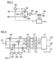
- FIG. 3 shows a schematic illustration of one embodiment of a transmitter with a feedback path.
- the transmitter includes a third input 301 and a fourth input 302 which may be used to supply the data signal for transmission in the form of a Quadrature-modulated baseband signal.
- an Inphase signal (I) is provided at the third input 301 and a Quadrature signal is provided at the fourth input 302 .
- These signals may be produced from a baseband-processing device such as a microprocessor.
- the third input 301 is connected to a first mixer 303 ; and the fourth input 302 is connected to a second mixer 304 .
- the transmitter has a local oscillator 305 .
- the output side of the local oscillator 305 is connected to the third mixer 303 and to a phase shifter 306 .
- a local frequency signal produced by the local oscillator 305 is supplied to the first mixer 303 .
- the second mixer 304 is supplied with a local frequency signal shifted by a phase, for example by pi/2 or 90°.
- the first mixer 303 and the second mixer 304 are connected to an input of a power amplifier 307 .
- An output of the power amplifier 307 is connected to a transmission output 309 via an output line 308 .
- the transmission output 309 may be connected to a transmission medium (not shown in FIG. 3 ).
- the transmission medium may be, in various embodiments, an antenna or a transmission line, such as a copper wire.
- Other transmission media are likewise conceivable, e.g. designed for optical transmission using an optical fiber.
- the transmitter shown in the FIG. 3 may include a transmission path which uses a Cartesian modulator, i.e. multiplicative mixing. This largely ensures a linear transmission chain.
- the output line 308 is electrically coupled to a return line 310 via a coupling element 309 .
- a portion of the return line 310 is routed parallel to the output line 308 in the coupling element 309 , so that the return line 310 has a parallel section.
- the return line 310 therefore has both ends of the parallel section connected to a switching element in a demodulator 311 .
- the demodulator 311 can be designed in the same way as the demodulator shown in FIG. 2 , for example. In one embodiment, it is particularly suitable for performing additive mixing.
- the local oscillator 305 is likewise connected to the demodulator 311 . It is therefore possible to dispense with a separate oscillator in the demodulator 311 for producing a second frequency signal for demodulating the return signal. In various embodiments, this is advantageously possible because the local frequency signal produced by the local oscillator 305 is not phase-modulated.
- the demodulator 311 takes the demodulated return signal and determines at least one signal level. Depending on how the return line is connected to the demodulator 311 , the signal level of an output signal from the transmitter or of a returning reflected signal present at the transmission output is determined as in the embodiment shown in FIG. 2 .
- the demodulator 211 may be designed in various embodiments, likewise as illustrated in FIG. 2 , to provide a reference baseband signal, for example, as a reference Inphase signal and as a reference Quadrature phase signal. However, this may be necessary if high demands have been placed on the linearity of the signal path.
- FIG. 4 shows a schematic illustration of one embodiment of a six-port junction receiver.
- the six-port junction receiver includes a first signal input 401 which is connected to a first adder 402 , to a second adder 403 , to a third adder 404 and to a fourth adder 405 in parallel.
- the six-port junction receiver also further includes a second signal input 406 which is connected to the first adder 402 and to a first phase shifter 407 .
- the output side of the first phase shifter 407 is connected to the second adder 404 and to a second phase shifter 408 .
- the output side of the second phase shifter 408 is connected to the third adder 404 and to a third phase shifter 409 .
- the output side of the third phase shifter 409 is connected to the fourth adder 405 .
- the output side of the first adder 402 is connected to an evaluation unit 412 via a first nonlinear transmission element 410 , for example, such as a diode with a square transmission characteristic, and via a first low-pass filter 411 .
- the output side of the second adder 403 is connected to the evaluation unit 412 via a second nonlinear transmission element 413 , for example, a diode with a square transmission characteristic, and via a second low-pass filter 414 .
- the output side of the third adder 404 is connected to the evaluation unit 412 via a third nonlinear transmission element 415 , for example, a diode with a square transmission characteristic, and via a third low-pass filter 416 .
- the output side of the fourth adder 405 is connected to the evaluation unit 412 via a fourth nonlinear transmission element 417 , for example a diode with a square transmission characteristic, and via a fourth low-pass filter 418 .
- the evaluation unit 412 has an Inphase output 419 , a Quadrature phase output 420 and a signal level output 421 .
- the six-port junction receiver may be arranged as a receiver 204 in the embodiments shown in FIG. 2 and in FIG. 3 respectively.
- the first signal input 401 is supplied with the return signal, subsequently called r(t).
- the second signal input 406 is supplied with the local frequency signal, subsequently called f(t).
- the return signal r(t) and the local frequency signal f(t) are added in four signal paths—respectively comprising an adder, a nonlinear transmission element and a low-pass filter—and the sum is squared and filtered.
- the four signal paths differ by virtue of the phase of the local frequency signal f(t). The phase difference is useful for subsequently reconstructing a reference baseband signal or a signal level from the return signal in the evaluation unit 511 .
- FIG. 5 shows a schematic illustration of one embodiment of a five-port junction receiver.
- the five-port junction receiver includes a third signal input 501 which is connected to a fifth adder 502 , to a sixth adder 503 and to a seventh adder 504 in parallel.
- the five-port junction receiver also further includes a fourth signal input 505 which is connected to a fourth phase shifter 506 .
- the output side of the fourth phase shifter 506 is connected to the fifth adder 502 .
- the fourth signal input 505 is also connected to a fifth phase shifter 507 and to a sixth phase shifter 508 .
- the output side of the fifth phase shifter 507 is connected to the sixth adder 503 .
- the output side of the sixth phase shifter 508 is connected to the seventh adder 504 .
- the output side of the fifth adder 502 is connected to an evaluation unit 511 via a fifth nonlinear transmission element 509 , for example a diode with a square transmission characteristic, and via a fifth low-pass filter 510 .
- the output side of the sixth adder 503 is connected to the evaluation unit 511 via a sixth nonlinear transmission element 512 , for example a diode with a square transmission characteristic, and via a sixth low-pass filter 513 .
- the output side of the seventh adder 504 is connected to the evaluation unit 511 via a seventh nonlinear transmission element 514 , for example a diode with a square transmission characteristic, and via a seventh low-pass filter 515 .
- the evaluation unit 511 has an Inphase output 516 , a Quadrature output 517 and a signal level output 518 .
- the five-port junction receiver may be arranged as a receiver 204 in the embodiments shown in FIG. 2 and in FIG. 3 .
- the third signal input 501 is supplied with the return signal, subsequently called r(t).
- the fourth signal input 505 is supplied with the local frequency signal, subsequently called f(t).
- the return signal r(t) and the local frequency signal f(t) are added in three signal paths—respectively comprising an adder, a nonlinear transmission element and a low-pass filter—and the sum is squared and filtered.
- the three signal paths differ by virtue of the phase of the local frequency signal f(t). The phase difference is useful for subsequently reconstructing a reference baseband signal or a signal level from the return signal in the evaluation unit 511 .
Abstract
Description
Claims (30)
Applications Claiming Priority (3)
| Application Number | Priority Date | Filing Date | Title |
|---|---|---|---|
| DE102006016761A DE102006016761A1 (en) | 2006-04-10 | 2006-04-10 | Transmitter and method for transmitting a data signal |
| DE102006016761 | 2006-04-10 | ||
| DE102006016761.9 | 2006-04-10 |
Publications (2)
| Publication Number | Publication Date |
|---|---|
| US20070237256A1 US20070237256A1 (en) | 2007-10-11 |
| US7702032B2 true US7702032B2 (en) | 2010-04-20 |
Family
ID=38514475
Family Applications (1)
| Application Number | Title | Priority Date | Filing Date |
|---|---|---|---|
| US11/544,319 Expired - Fee Related US7702032B2 (en) | 2006-04-10 | 2006-10-06 | Transmitter and method of transmitting a signal |
Country Status (2)
| Country | Link |
|---|---|
| US (1) | US7702032B2 (en) |
| DE (1) | DE102006016761A1 (en) |
Cited By (1)
| Publication number | Priority date | Publication date | Assignee | Title |
|---|---|---|---|---|
| US10567154B1 (en) | 2018-11-21 | 2020-02-18 | The Regents Of The University Of Michigan | Ring oscillator based all-digital Bluetooth low energy transmitter |
Families Citing this family (3)
| Publication number | Priority date | Publication date | Assignee | Title |
|---|---|---|---|---|
| US8085869B2 (en) * | 2008-02-14 | 2011-12-27 | Broadcom Corporation | Configurable load impedance for power amplifier predistortion calibration |
| US8442457B2 (en) | 2009-09-08 | 2013-05-14 | Google Inc. | System and method for adaptive beamforming for specific absorption rate control |
| DE102013112548B4 (en) * | 2013-11-14 | 2022-04-21 | Fujitsu Technology Solutions Intellectual Property Gmbh | Transmission device, use of a transmission device and method |
Citations (11)
| Publication number | Priority date | Publication date | Assignee | Title |
|---|---|---|---|---|
| DE31120C (en) | R. WlLCOX in St. Kilda, Colonie Victoria, Australien | Propulsion device for ships | ||
| DE3821181A1 (en) | 1988-06-23 | 1989-12-28 | Licentia Gmbh | POWER CONTROL ARRANGEMENT |
| US5420536A (en) * | 1993-03-16 | 1995-05-30 | Victoria University Of Technology | Linearized power amplifier |
| US6233438B1 (en) * | 1998-03-26 | 2001-05-15 | Ericsson Inc. | Wide-range power control systems and methods for radio frequency transmitters and mobile radiotelephones |
| US20010044323A1 (en) * | 1997-10-21 | 2001-11-22 | Waylett Nicholas S. A. | Self-contained masthead units for cellular communication networks |
| US20020044613A1 (en) * | 2000-09-06 | 2002-04-18 | Veselin Brankovic | I/Q demodulator device with three power detectors and two A/D converters |
| US20020171476A1 (en) * | 2001-04-20 | 2002-11-21 | Hiroyuki Yamamoto | Negative feedback amplifier and method of controlling loop gain thereof |
| US20030038675A1 (en) * | 2001-08-20 | 2003-02-27 | Gailus Paul H. | Feedback loop with adjustable bandwidth |
| US20030109222A1 (en) * | 2001-12-12 | 2003-06-12 | Agere Systems, Inc. | Group delay precompensator for broadband radio frequency transmitter and method of operating the same |
| US20040002322A1 (en) * | 2002-01-10 | 2004-01-01 | Dragan Krupezevic | Five-port topology for direct down-conversion |
| US6704562B1 (en) * | 1999-06-16 | 2004-03-09 | Sony International (Europe) Gmbh | N-port receiver with RF/LO isolation |
Family Cites Families (1)
| Publication number | Priority date | Publication date | Assignee | Title |
|---|---|---|---|---|
| DD31120A1 (en) * | 1961-07-15 | 1964-09-05 | Rudolf Kuehn | Single-stroke mixing part for very high frequencies |
-
2006
- 2006-04-10 DE DE102006016761A patent/DE102006016761A1/en active Pending
- 2006-10-06 US US11/544,319 patent/US7702032B2/en not_active Expired - Fee Related
Patent Citations (11)
| Publication number | Priority date | Publication date | Assignee | Title |
|---|---|---|---|---|
| DE31120C (en) | R. WlLCOX in St. Kilda, Colonie Victoria, Australien | Propulsion device for ships | ||
| DE3821181A1 (en) | 1988-06-23 | 1989-12-28 | Licentia Gmbh | POWER CONTROL ARRANGEMENT |
| US5420536A (en) * | 1993-03-16 | 1995-05-30 | Victoria University Of Technology | Linearized power amplifier |
| US20010044323A1 (en) * | 1997-10-21 | 2001-11-22 | Waylett Nicholas S. A. | Self-contained masthead units for cellular communication networks |
| US6233438B1 (en) * | 1998-03-26 | 2001-05-15 | Ericsson Inc. | Wide-range power control systems and methods for radio frequency transmitters and mobile radiotelephones |
| US6704562B1 (en) * | 1999-06-16 | 2004-03-09 | Sony International (Europe) Gmbh | N-port receiver with RF/LO isolation |
| US20020044613A1 (en) * | 2000-09-06 | 2002-04-18 | Veselin Brankovic | I/Q demodulator device with three power detectors and two A/D converters |
| US20020171476A1 (en) * | 2001-04-20 | 2002-11-21 | Hiroyuki Yamamoto | Negative feedback amplifier and method of controlling loop gain thereof |
| US20030038675A1 (en) * | 2001-08-20 | 2003-02-27 | Gailus Paul H. | Feedback loop with adjustable bandwidth |
| US20030109222A1 (en) * | 2001-12-12 | 2003-06-12 | Agere Systems, Inc. | Group delay precompensator for broadband radio frequency transmitter and method of operating the same |
| US20040002322A1 (en) * | 2002-01-10 | 2004-01-01 | Dragan Krupezevic | Five-port topology for direct down-conversion |
Non-Patent Citations (2)
| Title |
|---|
| Of Hentschel ,The Six-Port as a Communications Receiver, IEEE Transactions on Microwave Theory and Techniques, vol. 53, No. 3, Mar. 2005, pp. 1039-1047. * |
| Tim Hentschel, The Six-Port as a Communication Reciever, IEEE Trans. on Microwave Theory and Technology, Vo. 53, No. 3, Mar. 2005. |
Cited By (1)
| Publication number | Priority date | Publication date | Assignee | Title |
|---|---|---|---|---|
| US10567154B1 (en) | 2018-11-21 | 2020-02-18 | The Regents Of The University Of Michigan | Ring oscillator based all-digital Bluetooth low energy transmitter |
Also Published As
| Publication number | Publication date |
|---|---|
| DE102006016761A1 (en) | 2007-10-18 |
| US20070237256A1 (en) | 2007-10-11 |
Similar Documents
| Publication | Publication Date | Title |
|---|---|---|
| US7817970B2 (en) | Transmitting/receiving device having a polar modulator with variable predistortion | |
| US7915954B2 (en) | Amplifier predistortion and autocalibration method and apparatus | |
| US7522676B2 (en) | Method and system for transmitter envelope delay calibration | |
| US6980604B2 (en) | Transmission device and transmission method | |
| US7072421B2 (en) | IQ modulation systems and methods that use separate phase and amplitude signal paths and perform modulation within a phase locked loop | |
| US7539268B2 (en) | Transmission/reception arrangement and method for reducing nonlinearities in output signals from a transmission/reception arrangement | |
| CN101167325B (en) | Polar modulation transmitter circuit and communications device | |
| Presti et al. | Closed-loop digital predistortion system with fast real-time adaptation applied to a handset WCDMA PA module | |
| JP4676383B2 (en) | Transmitter circuit and transmitter for mobile communication using the same | |
| US8326239B1 (en) | Power amplifier linearization using digital predistortion | |
| US20160173030A1 (en) | Method and Apparatus for Correcting Inconvenient Power Amplifier Load Characteristics in an Envelope Tracking Based System | |
| US8948700B2 (en) | Method and system for compensating for distortion in a transmitter by utilizing a digital predistortion scheme with a feedback mixer configuration | |
| US7702032B2 (en) | Transmitter and method of transmitting a signal | |
| WO2007116122A1 (en) | Measurement method and arrangement for amplitude and phase synchronization in a polar transmitter | |
| US7599669B2 (en) | Transmitting arrangement, transreceiver with a transmitting arrangement and method for signal processing | |
| KR101411170B1 (en) | Systems and methods of rf power transmission, modulation, and amplification | |
| US7773969B2 (en) | Current converter, frequency mixer, radiofrequency transmission system and method for frequency mixing | |
| Briffa | Linearization of RF power amplifiers | |
| KR101980862B1 (en) | Apparatus and methods for phase synchronization of local oscillators in a transceiver | |
| US6977968B1 (en) | Transmitting-receiving device comprising a closed cartesian feedback loop | |
| JP2011182267A (en) | Radio base station device | |
| Ahmed | Feedback linearization of RF power amplifier for TETRA standard | |
| JP2000201091A (en) | Frequency converting part and radio transmitter | |
| Tuovila | Characterization of an envelope tracking system for a mobile device | |
| Nielsen | Linearisation of RF Power Amplifiers |
Legal Events
| Date | Code | Title | Description |
|---|---|---|---|
| AS | Assignment |
Owner name: INFINEON TECHNOLOGIES AG, GERMANY Free format text: ASSIGNMENT OF ASSIGNORS INTEREST;ASSIGNOR:BOOS, ZDRAVKO;REEL/FRAME:018462/0677 Effective date: 20060925 Owner name: INFINEON TECHNOLOGIES AG,GERMANY Free format text: ASSIGNMENT OF ASSIGNORS INTEREST;ASSIGNOR:BOOS, ZDRAVKO;REEL/FRAME:018462/0677 Effective date: 20060925 |
|
| FEPP | Fee payment procedure |
Free format text: PAYOR NUMBER ASSIGNED (ORIGINAL EVENT CODE: ASPN); ENTITY STATUS OF PATENT OWNER: LARGE ENTITY |
|
| STCF | Information on status: patent grant |
Free format text: PATENTED CASE |
|
| AS | Assignment |
Owner name: INTEL MOBILE COMMUNICATIONS TECHNOLOGY GMBH, GERMA Free format text: ASSIGNMENT OF ASSIGNORS INTEREST;ASSIGNOR:INFINEON TECHNOLOGIES AG;REEL/FRAME:027548/0623 Effective date: 20110131 |
|
| AS | Assignment |
Owner name: INTEL MOBILE COMMUNICATIONS GMBH, GERMANY Free format text: ASSIGNMENT OF ASSIGNORS INTEREST;ASSIGNOR:INTEL MOBILE COMMUNICATIONS TECHNOLOGY GMBH;REEL/FRAME:027556/0709 Effective date: 20111031 |
|
| FPAY | Fee payment |
Year of fee payment: 4 |
|
| AS | Assignment |
Owner name: INTEL DEUTSCHLAND GMBH, GERMANY Free format text: CHANGE OF NAME;ASSIGNOR:INTEL MOBILE COMMUNICATIONS GMBH;REEL/FRAME:037057/0061 Effective date: 20150507 |
|
| MAFP | Maintenance fee payment |
Free format text: PAYMENT OF MAINTENANCE FEE, 8TH YEAR, LARGE ENTITY (ORIGINAL EVENT CODE: M1552) Year of fee payment: 8 |
|
| AS | Assignment |
Owner name: INTEL CORPORATION, CALIFORNIA Free format text: CONFIRMATORY ASSIGNMENT EFFECTIVE AS OF JANUARY 1, 2018;ASSIGNOR:INTEL DEUTSCHLAND GMBH;REEL/FRAME:053477/0001 Effective date: 20200615 |
|
| AS | Assignment |
Owner name: APPLE INC., CALIFORNIA Free format text: ASSIGNMENT OF ASSIGNORS INTEREST;ASSIGNOR:INTEL CORPORATION;REEL/FRAME:053518/0586 Effective date: 20191130 |
|
| FEPP | Fee payment procedure |
Free format text: MAINTENANCE FEE REMINDER MAILED (ORIGINAL EVENT CODE: REM.); ENTITY STATUS OF PATENT OWNER: LARGE ENTITY |
|
| LAPS | Lapse for failure to pay maintenance fees |
Free format text: PATENT EXPIRED FOR FAILURE TO PAY MAINTENANCE FEES (ORIGINAL EVENT CODE: EXP.); ENTITY STATUS OF PATENT OWNER: LARGE ENTITY |
|
| STCH | Information on status: patent discontinuation |
Free format text: PATENT EXPIRED DUE TO NONPAYMENT OF MAINTENANCE FEES UNDER 37 CFR 1.362 |
|
| FP | Lapsed due to failure to pay maintenance fee |
Effective date: 20220420 |