US7710083B2 - Electronic device, method for controlling the same, and optical semiconductor module - Google Patents
Electronic device, method for controlling the same, and optical semiconductor module Download PDFInfo
- Publication number
- US7710083B2 US7710083B2 US11/727,682 US72768207A US7710083B2 US 7710083 B2 US7710083 B2 US 7710083B2 US 72768207 A US72768207 A US 72768207A US 7710083 B2 US7710083 B2 US 7710083B2
- Authority
- US
- United States
- Prior art keywords
- voltage
- power supply
- converter
- electronic circuit
- electronic device
- Prior art date
- Legal status (The legal status is an assumption and is not a legal conclusion. Google has not performed a legal analysis and makes no representation as to the accuracy of the status listed.)
- Active, expires
Links
Images


Classifications
-
- H—ELECTRICITY
- H02—GENERATION; CONVERSION OR DISTRIBUTION OF ELECTRIC POWER
- H02J—CIRCUIT ARRANGEMENTS OR SYSTEMS FOR SUPPLYING OR DISTRIBUTING ELECTRIC POWER; SYSTEMS FOR STORING ELECTRIC ENERGY
- H02J1/00—Circuit arrangements for dc mains or dc distribution networks
- H02J1/06—Two-wire systems
-
- H—ELECTRICITY
- H02—GENERATION; CONVERSION OR DISTRIBUTION OF ELECTRIC POWER
- H02M—APPARATUS FOR CONVERSION BETWEEN AC AND AC, BETWEEN AC AND DC, OR BETWEEN DC AND DC, AND FOR USE WITH MAINS OR SIMILAR POWER SUPPLY SYSTEMS; CONVERSION OF DC OR AC INPUT POWER INTO SURGE OUTPUT POWER; CONTROL OR REGULATION THEREOF
- H02M3/00—Conversion of dc power input into dc power output
- H02M3/02—Conversion of dc power input into dc power output without intermediate conversion into ac
- H02M3/04—Conversion of dc power input into dc power output without intermediate conversion into ac by static converters
- H02M3/10—Conversion of dc power input into dc power output without intermediate conversion into ac by static converters using discharge tubes with control electrode or semiconductor devices with control electrode
- H02M3/145—Conversion of dc power input into dc power output without intermediate conversion into ac by static converters using discharge tubes with control electrode or semiconductor devices with control electrode using devices of a triode or transistor type requiring continuous application of a control signal
- H02M3/155—Conversion of dc power input into dc power output without intermediate conversion into ac by static converters using discharge tubes with control electrode or semiconductor devices with control electrode using devices of a triode or transistor type requiring continuous application of a control signal using semiconductor devices only
- H02M3/156—Conversion of dc power input into dc power output without intermediate conversion into ac by static converters using discharge tubes with control electrode or semiconductor devices with control electrode using devices of a triode or transistor type requiring continuous application of a control signal using semiconductor devices only with automatic control of output voltage or current, e.g. switching regulators
Definitions
- This invention generally relates to an electronic device, a method for controlling the same, and an optical semiconductor device. More particularly, the present invention relates to an electronic device equipped with a DC/DC converter, a method for controlling such an electronic device, and an optical semiconductor module.
- Electronic devices having electronic circuits are used in various fields.
- Electronic circuits built in the electronic devices are supplied as semiconductor devices such as integrated circuits.
- the electronic devices are supplied with a power supply voltage that falls within a defined range prescribed as a recommended operating condition.
- the recommended operating condition is an operating condition guaranteed by the supplier of the electronic circuits.
- the electronic circuits incorporated into the electronic devices are supplied with the power supply voltages within the range of the recommended operating condition.
- FIG. 1 is a block diagram of an electronic device 60 a equipped with an electronic circuit 50 .
- the electronic device 60 a may include multiple electronic circuits 50 .
- the electronic device 60 a has one electronic circuit 50 .
- the recommended operating condition for a power supply input to the electronic circuit 50 is assumed as Vc(1 ⁇ ) where Vc is the center value of the recommended operating condition for the voltage of the power supply input to the electronic circuit 50 , while the lower limit Vmin of the recommended operating condition is equal to Vc(1 ⁇ ) and the upper limit Vmax thereof is equal to Vc(1+ ⁇ ).
- the power supply inputs of the electronic circuit 50 are directly connected to an external power supply outside of the electronic device 60 a and ground. Generally, the power supply voltage Vc is applied to the electronic circuit 50 .
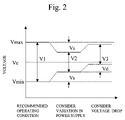
- FIG. 2 is a block diagram for explaining the voltage of an external power supply generally used. As shown in the left-side portion of FIG. 2 , the recommended operating condition for the power supply input voltage of the electronic circuit 50 ranges from Vmin to Vmax at the center of V 1 . When a variation (assumed as Vs) in the power supply voltage is considered, the usable range as the power supply input to the electronic circuit 50 is V 2 that ranges from Vmin+Vs to Vmax ⁇ Vs.
- the voltage supplied from the external power supply falls within a range V 3 of Vmin+Vs+Vd to Vmax ⁇ Vs+Vd.
- Vc voltage of the external power supply
- Vc voltage of the power supply input to the electronic circuit 50
- P of the electronic device 60 a that is, the electronic circuit 50
- Ic current consumed in the electronic circuit 50 as has been defined previously.
- Vmax is the allowable maximum voltage of the external power supply as long as the recommended operating condition of the power supply input to the electronic circuit 50 is satisfied.
- P max Vc (1+ ⁇ ) ⁇ Ic (1+ ⁇ ) (2) As described above, when the voltage of the external power supply varies, the power of the electronic device 60 a is changed.
- Japanese Patent Application Publication No. 2005-245152 discloses a DC/DC converter.
- the electronic devices are required to reduce power consumed in the internal electronic circuits.
- the present invention has been made taking the above into consideration and aims at reducing power consumed in electronic circuits.
- an electronic device including: a DC/DC converter supplied with an external power supply; and an electronic circuit having a power supply input to which an output of the DC/DC converter is supplied, a converted voltage that is the output of the DC/DC converter being lower than a center value of a recommended operating condition for a voltage of the power supply input of the electronic circuit.
- an optical semiconductor module including: a conversion circuit that performs a conversion between an electric signal and an optical signal; and an electronic device communicating with the conversion circuit, the electronic device including: a DC/DC converter supplied with an external power supply; and an electronic circuit having a power supply input to which an output of the DC/DC converter is supplied, a converted voltage that is the output of the DC/DC converter being lower than a center value of a recommended operating condition for a voltage of the power supply input of the electronic circuit.
- a method for controlling an electronic device equipped with an electronic circuit including: inputting an external power supply; converting a voltage of the external power supply into a voltage lower than a center value of a recommended operating condition for a voltage of the power supply input of the electronic circuit; and supplying a converted voltage to the electronic circuit.
- FIG. 1 is a block diagram of a conventional electronic device
- FIG. 2 is a block diagram of a power supply voltage used for the conventional electronic device shown in FIG. 1 ;
- FIG. 3 is a block diagram of an electronic device in accordance with a first embodiment
- FIG. 4 is a block diagram of explaining effects of the electronic device of the first embodiment
- FIG. 5 is a block diagram of a DC/DC converter used for the first embodiment
- FIG. 6 is a block diagram of a DC/DC converter and its peripheral circuit in accordance with a second embodiment
- FIG. 7 is a block diagram of an electronic device in accordance with a third embodiment.
- FIG. 8 is a block diagram of an optical semiconductor module in accordance with a fourth embodiment.
- FIG. 3 is a block diagram of an electronic device configured in accordance with a first embodiment of the present invention.
- an electronic device 60 has a DC/DC converter 20 having a conversion efficiency ⁇ .
- An external power supply is applied to an input “in” of the DC/DC converter 20 , and an output “out” thereof is applied to a power supply input of the electronic circuit 50 .
- the voltage of the external power supply may, for example, be the center value Vc of the recommended operating condition. However, an arbitrary voltage may be used.
- the DC/DC converter 20 converts an arbitrary voltage into a voltage Vcon, which is then applied to the electronic circuit 50 .
- the DC/DC converter 20 When the output of the DC/DC converter 20 is highly accurate with respect to Vc ⁇ (Vc ⁇ Vmin), the DC/DC converter 20 is capable of stably outputting the converted voltage Vcon even if the power supply voltage Vc varies.
- the power supply input to the electronic circuit 50 may be set to the lower limit Vmin of the recommended operating condition.
- the recommended operating condition of the power supply input to the electronic circuit 50 is 3.3 V ⁇ 5%.
- the external power supply outputs a voltage of 3.3 V ⁇ 5%.
- the electronic device 60 of the first embodiment consumes a reduced amount of power when the same external power supply as that for the conventional electronic device 60 a is used.
- the voltage at the output “out” of the DC/DC converter 20 is set lower than the center value Vc of the recommended operating condition for the power supply input to the electronic circuit 50 . It is thus possible to reduce power consumption of the electronic device 60 .
- the condition ⁇ >(1 ⁇ ) or ⁇ >1 ⁇ ( ⁇ + ⁇ ) reduces the power consumption of the electronic device 60 , as compared to the conventional electronic device 60 a with Vc of the external power supply.
- FIG. 5 is a block diagram of a step-down type of the DC/DC converter 20 in accordance with the first embodiment.
- a DC/DC converter circuit 21 includes a switching circuit 22 , a PWM (Pulse Width Modulation) generator circuit 24 , a differential amplifier 26 and a voltage source 28 .
- the output voltage of the DC/DC converter 20 is applied to a feedback terminal FB thereof.
- the differential amplifier 26 is supplied with the fed back voltage FB and a reference voltage of the voltage source 28 and amplifies the difference between these voltages.
- the voltage corresponding to the difference is applied to the PWM generator circuit 24 .
- the PWM generator circuit 24 adjusts the pulse width applied to the switching circuit 22 in accordance with the voltage from the differential amplifier 26 .
- the switching circuit 22 switches the voltage applied to the input terminal of the DC/DC converter 20 on the basis of the pulse signal from the PWM generator circuit 24 .
- An inductor 36 and a capacitor 38 function to remove high-frequency components from the output voltage from the switching circuit 22 , and the DC voltage thus regulated is finally output.
- the DC/DC converter 20 is not limited to the step-down type but may be of step-up type or Buck-Boost type.
- the voltage of the external power supply may be set higher than Vc.
- the step-up type DC/DC converter is used, the voltage of the external power supply may be set lower than Vc.
- the Buck-Boost type DC/DC converter the voltage of the external power supply may be equal to Vc. Since the step-down type DC/DC converter has a conversion efficiency of 95% or higher, it is suitable for the DC/DC converter 20 employed in the first embodiment.
- the Buck-Boost type DC/DC converter has a conversion efficiency as low as 90 to 95%, the voltage of the external power supply may be set equal to the power supply voltage of the electronic circuit 50 .
- this type of DC/DC converter has an interchangeability with the conventional electronic device 60 a.
- a second embodiment has an exemplary structure in which a circuit 40 for improving the accuracy of the output voltage of the DC/DC converter 20 is added thereto.
- FIG. 6 is a block diagram of a DC/DC converter having the circuit 40 for improving the accuracy of the output voltage of the DC/DC converter 20 shown in FIG. 5 .
- the other structures of the DC/DC converter are the same as those of the DC/DC converter 20 shown in FIG. 5 , and a description thereof will be omitted here while the identical reference numerals are assigned to the identical parts.
- the circuit 40 has a differential amplifier 42 and a voltage source 44 .
- the differential amplifier 42 amplifies the difference between the output voltage of the DC/DC converter 20 and a reference voltage of the voltage source 44 .
- the output voltage of the differential amplifier 42 is applied to the inverting input terminal of the differential amplifier 26 of the DC/DC converter circuit 21 via the feedback terminal FB.
- the circuit 40 feeds the output of the DC/DC converter 20 back to the feedback terminal FB.
- the DC/DC converter 20 is capable of regulating the output voltage more accurately. It is thus possible to supply the electronic circuit 50 with a power supply voltage closer to Vmin and reduce power consumed in the electronic circuit 60 .
- a third embodiment has an exemplary structure in which there is provided a voltage setting circuit 52 that outputs a voltage to the feedback terminal FB of the DC/DC converter 20 on the basis of the output of the DC/DC converter 20 .
- FIG. 7 is a block diagram of an electronic device 60 b in accordance with the third embodiment.
- the electronic device 60 b has a configuration obtained by adding the voltage setting circuit 52 to the electronic device 60 shown in FIG. 3 .
- the other structures of the electronic device 60 b are the same as those of the electronic device 60 , and a description thereof will be omitted here while the identical reference numerals are assigned to the identical parts.
- the output voltage of the DC/DC converter 20 is applied to an AD converter 58 of the voltage setting circuit 52 .
- the AD converter 58 converts the output voltage of the DC/DC converter 20 into a digital signal, which is applied to an external communication circuit 54 of the voltage setting circuit 52 .
- the external communication circuit 54 outputs the input digital signal to a controller 62 , which may be inside or outside of the electronic device 60 b .
- the controller 62 computes a voltage applied to the feedback terminal FB of the DC/DC converter so that the output voltage of the DC/DC converter 20 is regulated at a defined voltage on the basis of the digital signal from the voltage setting circuit 54 . Then, the controller 62 outputs a digital signal corresponding to the voltage thus computed to the external communication circuit 54 .
- the circuit 54 supplies a DA converter 56 of the voltage setting circuit 52 with the digital signal indicative of the voltage applied to the feedback terminal FB.
- the DA converter 56 converts the digital signal into a corresponding voltage, which is then applied to the DC/DC converter 20 .
- the voltage setting circuit 52 supplies the feedback terminal FB with the voltage computed so that the output voltage of the DC/DC converter 20 can be regulated at the defined voltage on the basis of the output voltage of the DC/DC converter 20 .
- the voltage setting circuit 52 may always feed the output of the DC/DC converter 20 back to the feedback terminal FB thereof.
- the voltage that is to be fed back to the feedback terminal FB may be determined when the electronic device 60 b is powered on or every certain constant time (at the time of calibration). That is, the controller 62 computes, at the time of calibration, the voltage applied to the feedback terminal FB of the DC/DC converter 20 on the basis of the output of the DC/DC converter 20 .
- the voltage setting circuit 52 retains the voltage thus computed and applies it to the feedback terminal FB until the next calibration.
- the feedback circuit for applying the voltage to the feedback terminal FB of the DC/DC converter 20 is not limited to the aforementioned circuit 40 employed in the second embodiment and the voltage setting circuit 52 in the third embodiment, but may have another configuration.
- a fourth embodiment is an optical semiconductor module, which is an example of the electronic device.
- FIG. 8 shows an optical module 10 in accordance with the fourth embodiment.
- the external power supply is applied to the DC/DC converter 20 .
- the output of the DC/DC converter 20 is applied to an electronic circuit that includes CDR (Clock and Data Recovery) circuits 11 and 16 , a limiting amplifier 12 , an ROSA (Receiver Optical Sub Assembly) 13 , an LD (Laser Diode) driver 17 , and TOSA (Transmitter Optical Sub Assembly) 18 .
- the DC/DC converter 20 operates in the same manner as that of the first embodiment.
- the optical semiconductor module 10 has such a function that a laser diode in the TOSA 18 converts an electric input signal into an optical signal, which is then output to an optical fiber, and has another function such that a photodiode in the ROSA 13 converts an optical signal from the optical fiber into an electric signal.
- the optical semiconductor module is required to operate with reduced power consumption.
- the optical semiconductor module shown in FIG. 8 meets the above requirement.
- the optical semiconductor module of the present invention may include either a semiconductor light-emitting device such as a semiconductor laser diode or LED, or a semiconductor light-receiving device such as a photodiode, or both.
- the optical semiconductor module of the present invention may include an optical semiconductor module capable of converting an electric signal into an optical signal, or another optical semiconductor module capable of converting an optical signal into an electric signal.
- the electronic device of the second or third embodiment may be embedded in the optical semiconductor module.
- the electronic devices of the first through third embodiments may be a portable electronic device or part thereof, such as a notebook personal computer, a portable phone, radio, audio, camera or PDA.
- the portable electronic device is particularly required to operate with reduced power consumption.
- the portable electronic device of the present invention consumes reduced power and operates more efficiently.
- the present invention may be an in-vehicle electronic device such as a car navigation system, a car audio system or an in-vehicle DVD.
- the recommended operating conditions for the electronic circuits guarantee the stable operation thereof.
- the electronic circuit When an electronic circuit is supplied with a power supply lower than the center value of the recommended operating condition, the electronic circuit may operate unstably. However, the unstable operation should be avoided.
- the DC/DC converter is originally a power supply circuit capable of setting up the voltage. The setting up of voltage is realized by storing charge from the external power supply in a capacitor and then discharging it.
- the electronic devices of the first through third embodiments have the DC/DC converters via which the external power is applied to the electronic circuits. It is thus possible to stabilize the voltage of the power supply and supply the electronic circuit with the power supply lower than the center value of the voltage range that meets the recommended operating condition.
Abstract
Description
P=Vc×Ic (1)
where Ic is current consumed in the
Pmax=Vc(1+α)×Ic(1+β) (2)
As described above, when the voltage of the external power supply varies, the power of the
P=(Vc(1−α)×Ic(1−β))/η (3)
Pmax=(Vc(1−α)×Ic(1−β))/η (4)
It can be seen from the above that the
P=3.3 V×0.3 A=0.99 W
Pmax=(3.3 V×1.05)×(0.3 A×1.03)=1.07 W.
P=(3.3 V×0.95)×(0.3 A×0.97)/η=0.96 W
Pmax=(3.3 V×0.95)×(0.3 A×0.97)/η=0.96 W
Vc×Ic>(Vc(1−β)×Ic)/η
that is,
η>(1−λ)
η>(1−λ)×(1−γ)
η>1−(λ+γ)
λ×γ=0.05×0.03=0.0015.
Claims (8)
η>(1−λ)
η>1(λ+γ)
η>(1−λ)
η>(1−λ)
η>1−(λ+γ)
Applications Claiming Priority (2)
| Application Number | Priority Date | Filing Date | Title |
|---|---|---|---|
| JP2006-096050 | 2006-03-30 | ||
| JP2006096050A JP4650947B2 (en) | 2006-03-30 | 2006-03-30 | Electronic device, control method thereof, and optical semiconductor module |
Publications (2)
| Publication Number | Publication Date |
|---|---|
| US20070229040A1 US20070229040A1 (en) | 2007-10-04 |
| US7710083B2 true US7710083B2 (en) | 2010-05-04 |
Family
ID=38557879
Family Applications (1)
| Application Number | Title | Priority Date | Filing Date |
|---|---|---|---|
| US11/727,682 Active 2028-05-10 US7710083B2 (en) | 2006-03-30 | 2007-03-28 | Electronic device, method for controlling the same, and optical semiconductor module |
Country Status (2)
| Country | Link |
|---|---|
| US (1) | US7710083B2 (en) |
| JP (1) | JP4650947B2 (en) |
Families Citing this family (3)
| Publication number | Priority date | Publication date | Assignee | Title |
|---|---|---|---|---|
| JP2008236551A (en) * | 2007-03-22 | 2008-10-02 | Nec Corp | Transceiver for optical transmission and transmission method for the same |
| JP6687425B2 (en) * | 2015-07-31 | 2020-04-22 | 株式会社小糸製作所 | Lighting circuit and vehicle lamp using the same |
| KR101822280B1 (en) * | 2016-05-04 | 2018-01-26 | 현대자동차주식회사 | Method for correcting output voltage sensing error of low voltage dc-dc converter |
Citations (12)
| Publication number | Priority date | Publication date | Assignee | Title |
|---|---|---|---|---|
| US6091940A (en) * | 1998-10-21 | 2000-07-18 | Parkervision, Inc. | Method and system for frequency up-conversion |
| US6154015A (en) * | 1998-07-14 | 2000-11-28 | Ricoh Company, Ltd. | DC-DC converter |
| US6229932B1 (en) * | 1997-11-26 | 2001-05-08 | Hitachi, Ltd. | Optical signal switching apparatus |
| JP2004208365A (en) | 2002-12-24 | 2004-07-22 | Ricoh Co Ltd | Switching power supply |
| US20050047181A1 (en) | 2003-08-29 | 2005-03-03 | Isao Yamamoto | Power supply apparatus |
| JP2005245152A (en) | 2004-02-27 | 2005-09-08 | Toko Inc | Dc/dc converter |
| US20060001409A1 (en) * | 2004-07-02 | 2006-01-05 | Rohm Co., Ltd. | DC/DC converter |
| US7031615B2 (en) * | 2001-10-04 | 2006-04-18 | Finisar Corporation | Optical channel selection and evaluation system |
| US20060208718A1 (en) * | 2003-04-28 | 2006-09-21 | Shohichi Nitta | Step-up/down dc-dc converter |
| US7173377B2 (en) * | 2004-05-24 | 2007-02-06 | Samsung Sdi Co., Ltd. | Light emission device and power supply therefor |
| US20070195565A1 (en) * | 2004-07-12 | 2007-08-23 | Murata Manufacturing Co., Ltd. | Dc-dc converter |
| US7321735B1 (en) * | 1998-10-21 | 2008-01-22 | Parkervision, Inc. | Optical down-converter using universal frequency translation technology |
Family Cites Families (1)
| Publication number | Priority date | Publication date | Assignee | Title |
|---|---|---|---|---|
| JP4512938B2 (en) * | 2003-08-22 | 2010-07-28 | 寛一 大杉 | Light-emitting diode lamp powered by dynamo |
-
2006
- 2006-03-30 JP JP2006096050A patent/JP4650947B2/en active Active
-
2007
- 2007-03-28 US US11/727,682 patent/US7710083B2/en active Active
Patent Citations (13)
| Publication number | Priority date | Publication date | Assignee | Title |
|---|---|---|---|---|
| US6229932B1 (en) * | 1997-11-26 | 2001-05-08 | Hitachi, Ltd. | Optical signal switching apparatus |
| US6154015A (en) * | 1998-07-14 | 2000-11-28 | Ricoh Company, Ltd. | DC-DC converter |
| US7321735B1 (en) * | 1998-10-21 | 2008-01-22 | Parkervision, Inc. | Optical down-converter using universal frequency translation technology |
| US6091940A (en) * | 1998-10-21 | 2000-07-18 | Parkervision, Inc. | Method and system for frequency up-conversion |
| US7031615B2 (en) * | 2001-10-04 | 2006-04-18 | Finisar Corporation | Optical channel selection and evaluation system |
| JP2004208365A (en) | 2002-12-24 | 2004-07-22 | Ricoh Co Ltd | Switching power supply |
| US20060208718A1 (en) * | 2003-04-28 | 2006-09-21 | Shohichi Nitta | Step-up/down dc-dc converter |
| JP2005080395A (en) | 2003-08-29 | 2005-03-24 | Rohm Co Ltd | Power supply device |
| US20050047181A1 (en) | 2003-08-29 | 2005-03-03 | Isao Yamamoto | Power supply apparatus |
| JP2005245152A (en) | 2004-02-27 | 2005-09-08 | Toko Inc | Dc/dc converter |
| US7173377B2 (en) * | 2004-05-24 | 2007-02-06 | Samsung Sdi Co., Ltd. | Light emission device and power supply therefor |
| US20060001409A1 (en) * | 2004-07-02 | 2006-01-05 | Rohm Co., Ltd. | DC/DC converter |
| US20070195565A1 (en) * | 2004-07-12 | 2007-08-23 | Murata Manufacturing Co., Ltd. | Dc-dc converter |
Non-Patent Citations (1)
| Title |
|---|
| Japanese Notification of Reason(s) for Refusal dated Dec. 8, 2009, issued in Japanese patent application No. 2006-096050. |
Also Published As
| Publication number | Publication date |
|---|---|
| JP2007274797A (en) | 2007-10-18 |
| JP4650947B2 (en) | 2011-03-16 |
| US20070229040A1 (en) | 2007-10-04 |
Similar Documents
| Publication | Publication Date | Title |
|---|---|---|
| US9523990B2 (en) | Control circuit of step-down DC-DC converter, control circuit of step-up DC-DC converter and step-up/step-down DC-DC converter | |
| US8174209B2 (en) | DC-DC converter and method for minimizing battery peak pulse loading | |
| US9154037B2 (en) | Current-mode buck converter and electronic system using the same | |
| US8749213B2 (en) | Mixed mode control for switching regulator with fast transient responses | |
| US8324825B2 (en) | Method and circuit for driving a low voltage light emitting diode | |
| US20060181340A1 (en) | Regulating charge pump | |
| US8989598B2 (en) | Power-saving driver circuit for providing a bias current or driving a current-driven load | |
| US20070262763A1 (en) | Power supply circuit device and electronic apparatus provided therewith | |
| JP2006187187A (en) | Power supply and light-emitting device using the same, electronic apparatus | |
| US7646153B2 (en) | Switching regulator | |
| US20090184699A1 (en) | Power supply apparatus and power supply method | |
| EP2312569B1 (en) | Apparatus for controlling power consumption of light source in mobile projector | |
| US20100045252A1 (en) | Power supply circuit | |
| US20160134246A1 (en) | Apparatus and method for high-efficiency envelope amplifier using adjustment of switch current | |
| JP2007242886A (en) | Light emitting element driving circuit, and portable device equipped therewith | |
| US7710083B2 (en) | Electronic device, method for controlling the same, and optical semiconductor module | |
| JP2009136097A (en) | Dc/dc converter, control circuit for the same, and electronic appliance using the same | |
| KR20080076735A (en) | Detection circuit and power supply system | |
| US20070200542A1 (en) | Voltage regulating power supply for noise sensitive circuits | |
| US9214860B2 (en) | Comparator multiplexing LDO and converted output to DC-DC converter circuitry | |
| KR20100066267A (en) | Apparatus for detecting current, and driver for light emitting diode comprising the same | |
| JP4974653B2 (en) | Step-up switching regulator control circuit, step-up switching regulator using the same, and electronic equipment using them | |
| US8018207B2 (en) | Switching regulator | |
| JP4467395B2 (en) | Power supply | |
| US7415053B2 (en) | Optical transmitter with a least pair of semiconductor laser diodes |
Legal Events
| Date | Code | Title | Description |
|---|---|---|---|
| AS | Assignment |
Owner name: EUDYNA DEVICES INC., JAPAN Free format text: ASSIGNMENT OF ASSIGNORS INTEREST;ASSIGNOR:INOUE, SHINGO;REEL/FRAME:019155/0652 Effective date: 20070319 Owner name: EUDYNA DEVICES INC.,JAPAN Free format text: ASSIGNMENT OF ASSIGNORS INTEREST;ASSIGNOR:INOUE, SHINGO;REEL/FRAME:019155/0652 Effective date: 20070319 |
|
| STCF | Information on status: patent grant |
Free format text: PATENTED CASE |
|
| FEPP | Fee payment procedure |
Free format text: PAYOR NUMBER ASSIGNED (ORIGINAL EVENT CODE: ASPN); ENTITY STATUS OF PATENT OWNER: LARGE ENTITY |
|
| FPAY | Fee payment |
Year of fee payment: 4 |
|
| MAFP | Maintenance fee payment |
Free format text: PAYMENT OF MAINTENANCE FEE, 8TH YEAR, LARGE ENTITY (ORIGINAL EVENT CODE: M1552) Year of fee payment: 8 |
|
| MAFP | Maintenance fee payment |
Free format text: PAYMENT OF MAINTENANCE FEE, 12TH YEAR, LARGE ENTITY (ORIGINAL EVENT CODE: M1553); ENTITY STATUS OF PATENT OWNER: LARGE ENTITY Year of fee payment: 12 |