US7712675B2 - Physical items for holding data securely, and methods and apparatus for publishing and reading them - Google Patents

Physical items for holding data securely, and methods and apparatus for publishing and reading them Download PDF

Info

Publication number
US7712675B2
US7712675B2 US11/493,031 US49303106A US7712675B2 US 7712675 B2 US7712675 B2 US 7712675B2 US 49303106 A US49303106 A US 49303106A US 7712675 B2 US7712675 B2 US 7712675B2
Authority
US
United States
Prior art keywords
data
memory
memory tag
memory circuit
tag
Prior art date
Legal status (The legal status is an assumption and is not a legal conclusion. Google has not performed a legal analysis and makes no representation as to the accuracy of the status listed.)
Active, expires
Application number
US11/493,031
Other versions
US20070095928A1 (en
Inventor
Helen Balinsky
Weng Wah Loh
Fraser John Dickin
Thomas Rathbone
Stefek Malkowski Zaba
Keith Alexander Harrison
John Waters
James Thomas Edward McDonnell
Current Assignee (The listed assignees may be inaccurate. Google has not performed a legal analysis and makes no representation or warranty as to the accuracy of the list.)
Hewlett Packard Development Co LP
Original Assignee
Hewlett Packard Development Co LP
Priority date (The priority date is an assumption and is not a legal conclusion. Google has not performed a legal analysis and makes no representation as to the accuracy of the date listed.)
Filing date
Publication date
Priority claimed from GB0300906A external-priority patent/GB2397272B/en
Application filed by Hewlett Packard Development Co LP filed Critical Hewlett Packard Development Co LP
Priority to US11/493,031 priority Critical patent/US7712675B2/en
Assigned to HEWLETT-PACKARD DEVELOPMENT COMPANY, L.P. reassignment HEWLETT-PACKARD DEVELOPMENT COMPANY, L.P. ASSIGNMENT OF ASSIGNORS INTEREST (SEE DOCUMENT FOR DETAILS). Assignors: HEWLETT-PACKARD LIMITED
Publication of US20070095928A1 publication Critical patent/US20070095928A1/en
Application granted granted Critical
Publication of US7712675B2 publication Critical patent/US7712675B2/en
Active legal-status Critical Current
Adjusted expiration legal-status Critical

Links

Images

Classifications

    • GPHYSICS
    • G06COMPUTING; CALCULATING OR COUNTING
    • G06KGRAPHICAL DATA READING; PRESENTATION OF DATA; RECORD CARRIERS; HANDLING RECORD CARRIERS
    • G06K19/00Record carriers for use with machines and with at least a part designed to carry digital markings
    • G06K19/06Record carriers for use with machines and with at least a part designed to carry digital markings characterised by the kind of the digital marking, e.g. shape, nature, code
    • G06K19/067Record carriers with conductive marks, printed circuits or semiconductor circuit elements, e.g. credit or identity cards also with resonating or responding marks without active components
    • G06K19/07Record carriers with conductive marks, printed circuits or semiconductor circuit elements, e.g. credit or identity cards also with resonating or responding marks without active components with integrated circuit chips
    • G06K19/073Special arrangements for circuits, e.g. for protecting identification code in memory
    • GPHYSICS
    • G06COMPUTING; CALCULATING OR COUNTING
    • G06FELECTRIC DIGITAL DATA PROCESSING
    • G06F21/00Security arrangements for protecting computers, components thereof, programs or data against unauthorised activity
    • G06F21/30Authentication, i.e. establishing the identity or authorisation of security principals
    • G06F21/31User authentication
    • G06F21/34User authentication involving the use of external additional devices, e.g. dongles or smart cards
    • G06F21/35User authentication involving the use of external additional devices, e.g. dongles or smart cards communicating wirelessly
    • GPHYSICS
    • G06COMPUTING; CALCULATING OR COUNTING
    • G06KGRAPHICAL DATA READING; PRESENTATION OF DATA; RECORD CARRIERS; HANDLING RECORD CARRIERS
    • G06K19/00Record carriers for use with machines and with at least a part designed to carry digital markings
    • G06K19/02Record carriers for use with machines and with at least a part designed to carry digital markings characterised by the selection of materials, e.g. to avoid wear during transport through the machine
    • G06K19/025Record carriers for use with machines and with at least a part designed to carry digital markings characterised by the selection of materials, e.g. to avoid wear during transport through the machine the material being flexible or adapted for folding, e.g. paper or paper-like materials used in luggage labels, identification tags, forms or identification documents carrying RFIDs
    • GPHYSICS
    • G06COMPUTING; CALCULATING OR COUNTING
    • G06KGRAPHICAL DATA READING; PRESENTATION OF DATA; RECORD CARRIERS; HANDLING RECORD CARRIERS
    • G06K19/00Record carriers for use with machines and with at least a part designed to carry digital markings
    • G06K19/06Record carriers for use with machines and with at least a part designed to carry digital markings characterised by the kind of the digital marking, e.g. shape, nature, code
    • G06K19/067Record carriers with conductive marks, printed circuits or semiconductor circuit elements, e.g. credit or identity cards also with resonating or responding marks without active components
    • G06K19/07Record carriers with conductive marks, printed circuits or semiconductor circuit elements, e.g. credit or identity cards also with resonating or responding marks without active components with integrated circuit chips
    • G06K19/073Special arrangements for circuits, e.g. for protecting identification code in memory
    • G06K19/07309Means for preventing undesired reading or writing from or onto record carriers
    • G06K19/07372Means for preventing undesired reading or writing from or onto record carriers by detecting tampering with the circuit
    • GPHYSICS
    • G06COMPUTING; CALCULATING OR COUNTING
    • G06KGRAPHICAL DATA READING; PRESENTATION OF DATA; RECORD CARRIERS; HANDLING RECORD CARRIERS
    • G06K19/00Record carriers for use with machines and with at least a part designed to carry digital markings
    • G06K19/06Record carriers for use with machines and with at least a part designed to carry digital markings characterised by the kind of the digital marking, e.g. shape, nature, code
    • G06K19/067Record carriers with conductive marks, printed circuits or semiconductor circuit elements, e.g. credit or identity cards also with resonating or responding marks without active components
    • G06K19/07Record carriers with conductive marks, printed circuits or semiconductor circuit elements, e.g. credit or identity cards also with resonating or responding marks without active components with integrated circuit chips
    • G06K19/077Constructional details, e.g. mounting of circuits in the carrier
    • G06K19/07749Constructional details, e.g. mounting of circuits in the carrier the record carrier being capable of non-contact communication, e.g. constructional details of the antenna of a non-contact smart card
    • G06K19/07758Constructional details, e.g. mounting of circuits in the carrier the record carrier being capable of non-contact communication, e.g. constructional details of the antenna of a non-contact smart card arrangements for adhering the record carrier to further objects or living beings, functioning as an identification tag
    • GPHYSICS
    • G06COMPUTING; CALCULATING OR COUNTING
    • G06QINFORMATION AND COMMUNICATION TECHNOLOGY [ICT] SPECIALLY ADAPTED FOR ADMINISTRATIVE, COMMERCIAL, FINANCIAL, MANAGERIAL OR SUPERVISORY PURPOSES; SYSTEMS OR METHODS SPECIALLY ADAPTED FOR ADMINISTRATIVE, COMMERCIAL, FINANCIAL, MANAGERIAL OR SUPERVISORY PURPOSES, NOT OTHERWISE PROVIDED FOR
    • G06Q20/00Payment architectures, schemes or protocols
    • G06Q20/30Payment architectures, schemes or protocols characterised by the use of specific devices or networks
    • G06Q20/32Payment architectures, schemes or protocols characterised by the use of specific devices or networks using wireless devices
    • G06Q20/327Short range or proximity payments by means of M-devices
    • G06Q20/3278RFID or NFC payments by means of M-devices
    • GPHYSICS
    • G06COMPUTING; CALCULATING OR COUNTING
    • G06QINFORMATION AND COMMUNICATION TECHNOLOGY [ICT] SPECIALLY ADAPTED FOR ADMINISTRATIVE, COMMERCIAL, FINANCIAL, MANAGERIAL OR SUPERVISORY PURPOSES; SYSTEMS OR METHODS SPECIALLY ADAPTED FOR ADMINISTRATIVE, COMMERCIAL, FINANCIAL, MANAGERIAL OR SUPERVISORY PURPOSES, NOT OTHERWISE PROVIDED FOR
    • G06Q20/00Payment architectures, schemes or protocols
    • G06Q20/30Payment architectures, schemes or protocols characterised by the use of specific devices or networks
    • G06Q20/34Payment architectures, schemes or protocols characterised by the use of specific devices or networks using cards, e.g. integrated circuit [IC] cards or magnetic cards
    • G06Q20/341Active cards, i.e. cards including their own processing means, e.g. including an IC or chip
    • GPHYSICS
    • G06COMPUTING; CALCULATING OR COUNTING
    • G06QINFORMATION AND COMMUNICATION TECHNOLOGY [ICT] SPECIALLY ADAPTED FOR ADMINISTRATIVE, COMMERCIAL, FINANCIAL, MANAGERIAL OR SUPERVISORY PURPOSES; SYSTEMS OR METHODS SPECIALLY ADAPTED FOR ADMINISTRATIVE, COMMERCIAL, FINANCIAL, MANAGERIAL OR SUPERVISORY PURPOSES, NOT OTHERWISE PROVIDED FOR
    • G06Q20/00Payment architectures, schemes or protocols
    • G06Q20/30Payment architectures, schemes or protocols characterised by the use of specific devices or networks
    • G06Q20/34Payment architectures, schemes or protocols characterised by the use of specific devices or networks using cards, e.g. integrated circuit [IC] cards or magnetic cards
    • G06Q20/346Cards serving only as information carrier of service
    • GPHYSICS
    • G06COMPUTING; CALCULATING OR COUNTING
    • G06QINFORMATION AND COMMUNICATION TECHNOLOGY [ICT] SPECIALLY ADAPTED FOR ADMINISTRATIVE, COMMERCIAL, FINANCIAL, MANAGERIAL OR SUPERVISORY PURPOSES; SYSTEMS OR METHODS SPECIALLY ADAPTED FOR ADMINISTRATIVE, COMMERCIAL, FINANCIAL, MANAGERIAL OR SUPERVISORY PURPOSES, NOT OTHERWISE PROVIDED FOR
    • G06Q20/00Payment architectures, schemes or protocols
    • G06Q20/30Payment architectures, schemes or protocols characterised by the use of specific devices or networks
    • G06Q20/34Payment architectures, schemes or protocols characterised by the use of specific devices or networks using cards, e.g. integrated circuit [IC] cards or magnetic cards
    • G06Q20/352Contactless payments by cards
    • GPHYSICS
    • G06COMPUTING; CALCULATING OR COUNTING
    • G06QINFORMATION AND COMMUNICATION TECHNOLOGY [ICT] SPECIALLY ADAPTED FOR ADMINISTRATIVE, COMMERCIAL, FINANCIAL, MANAGERIAL OR SUPERVISORY PURPOSES; SYSTEMS OR METHODS SPECIALLY ADAPTED FOR ADMINISTRATIVE, COMMERCIAL, FINANCIAL, MANAGERIAL OR SUPERVISORY PURPOSES, NOT OTHERWISE PROVIDED FOR
    • G06Q20/00Payment architectures, schemes or protocols
    • G06Q20/38Payment protocols; Details thereof
    • G06Q20/40Authorisation, e.g. identification of payer or payee, verification of customer or shop credentials; Review and approval of payers, e.g. check credit lines or negative lists
    • G06Q20/401Transaction verification
    • G06Q20/4014Identity check for transactions
    • G06Q20/40145Biometric identity checks
    • GPHYSICS
    • G07CHECKING-DEVICES
    • G07FCOIN-FREED OR LIKE APPARATUS
    • G07F7/00Mechanisms actuated by objects other than coins to free or to actuate vending, hiring, coin or paper currency dispensing or refunding apparatus
    • G07F7/08Mechanisms actuated by objects other than coins to free or to actuate vending, hiring, coin or paper currency dispensing or refunding apparatus by coded identity card or credit card or other personal identification means
    • G07F7/0806Details of the card
    • G07F7/0833Card having specific functional components
    • GPHYSICS
    • G07CHECKING-DEVICES
    • G07FCOIN-FREED OR LIKE APPARATUS
    • G07F7/00Mechanisms actuated by objects other than coins to free or to actuate vending, hiring, coin or paper currency dispensing or refunding apparatus
    • G07F7/08Mechanisms actuated by objects other than coins to free or to actuate vending, hiring, coin or paper currency dispensing or refunding apparatus by coded identity card or credit card or other personal identification means
    • G07F7/10Mechanisms actuated by objects other than coins to free or to actuate vending, hiring, coin or paper currency dispensing or refunding apparatus by coded identity card or credit card or other personal identification means together with a coded signal, e.g. in the form of personal identification information, like personal identification number [PIN] or biometric data
    • G07F7/1008Active credit-cards provided with means to personalise their use, e.g. with PIN-introduction/comparison system

Definitions

  • the invention relates to secure physical items (such as documents), to methods by which they can be created, and to methods by which they can be read. Aspects of the invention are particularly suitable for use in physical credentials (such as passbooks), either to identify an authorised bearer (such as passports) or to allow access by an authorised bearer to an asset (such as bank books).
  • physical credentials such as passbooks
  • an authorised bearer such as passports
  • an asset such as bank books
  • the invention provides a physical object, comprising one or more memory circuits adapted to be read wirelessly by a reader device attached to or incorporated within the physical object, wherein data in the memory circuit is protected from access by an unauthorised reader, wherein data in the memory circuit is adapted to identify an authorised bearer of the physical object, and wherein data in the memory circuit is adapted to allow access to a specified asset or assets by the authorised bearer.
  • FIG. 1 illustrates a sheet of paper annotated with electronic data in a manner illustrative of an embodiment of the invention
  • FIG. 2 illustrates an RFID memory tag suitable for use in the embodiments of the invention
  • FIG. 3 illustrates the circuitry of the memory tag of FIG. 2 and of a read/write device for wireless communication with the memory tag;
  • FIG. 4 is a schematic of the main elements of a printing device suitable for executing a method according to embodiments of the invention from the side;
  • FIG. 5 is a schematic of the apparatus of FIG. 4 from above;
  • FIG. 6 is a block diagram of the control of the apparatus of FIGS. 4 and 5 ;
  • FIG. 7 describes a tamper-evident security feature for a security document with respect to physical tampering
  • FIG. 8 describes a tamper-resistant security feature for a security document with respect to physical tampering
  • FIG. 9 shows a security document according to an embodiment of the invention and a method for reading it
  • FIG. 10 shows a method of publishing a security document according to an embodiment of the invention
  • FIG. 11 shows a method of reading a security document according to an embodiment of the invention
  • FIG. 12 shows schematically a memory tag and reader according to an embodiment of the invention
  • FIG. 13 shows a prior art data packet structure and a data packet structure for use in authenticating a memory tag according to an embodiment of the invention
  • FIG. 14 shows a flow diagram depicting a process of authenticating a memory tag according to an embodiment of the invention
  • FIG. 15 shows a flow diagram depicting a process of authenticating data stored on a memory tag according to an embodiment of the invention
  • FIG. 16 shows a physical object according to a further embodiment of the invention.
  • FIG. 17 shows initialisation of a memory tag in a physical object in accordance with a further embodiment of the invention.
  • FIG. 18 shows authentication of an authorised bearer of a physical object in accordance with a further embodiment of the invention.
  • the memory spot can be accessed wireless (and is preferably also wirelessly powered, most conveniently) inductively powered, it can be embedded in the document, allowing forms of tamperproofing that involve physical isolation from potential attacks. Data can be held which personalises the document to a user in a way that is not readily obvious (for example, an image of the user held electronically in a document which itself contains no visible image of the user).
  • the memory spot can be provided with processing power to enable a security exchange to be conducted with a reader so as to prevent unauthorised readers from gaining access to the retained information in any useful form. Specific elements used by embodiments of the invention will be described before full embodiments of the invention are themselves described.
  • FIGS. 1 to 3 a particularly suitable technology by which memory circuits can be attached to or incorporated within printed documents to enable security documents according to embodiments of the invention to be produced.
  • the memory circuits described are a form of inductively powered circuit read and written by radio-frequency communication—as such they resemble the existing RFID tag—but it will be appreciated by the skilled person that alternative forms of memory circuit may also be employable for the purpose described.
  • FIGS. 4 to 6 an exemplary method of printing documents whose content for is divided between a printed document and one or more memory circuits attached to or incorporated within printed documents—the publishing of such documents will also be discussed, particularly in the context of security documents.
  • FIGS. 7 and 8 There will then be described, with reference to FIGS. 7 and 8 , approaches that may be employed to physical isolation of a memory tag using tamper resistant or tamper evident technologies. After this, there will be described approaches for protecting information stored in a memory tag against reading by an unauthorised reader.
  • a memory tag with processing capabilities particularly suitable for use in certain embodiments of the invention is discussed with reference to FIGS. 12 to 15 .
  • FIG. 9 shows a physical item according to an embodiment of the invention, together with methods of publishing and reading such items in FIGS. 10 and 11 .
  • FIG. 16 onwards illustrate a further embodiment of the invention in which the physical item includes data hidden by steganography.
  • FIG. 1 illustrates an item, in this case a sheet of paper 10 , bearing printing 12 , which has been annotated with electronic data using a plurality of memory tags 14 .
  • the memory tags 14 have been secured to the sheet of paper 10 at various locations over its surface, although they may alternatively be embedded in the paper sheet 10 , preferably in locations identified by the printing 12 , in order to assist in locating them for the purposes of reading data from or writing data to the memory tags 14 .
  • a hand held reader device 16 is used to communicate with the memory tags 14 in wireless manner, as will be discussed further below.
  • the reader device 16 is also connected to a host computer, display, data rendering device or other apparatus 18 to which the data read from the memory tags 14 is passed.
  • reader device 16 will also be able to write to the memory tags 14 —however, in the case of security documents, this will either be prevented, or such writing will only be in addition to, rather than to replace, security data stored within the memory tag 14 .
  • the memory tag 14 is an RFID memory tag provided on a chip, and comprises an RFID transponder circuit 20 , a memory 22 , a power supply capacitor 24 and an antenna coil 26 having only a few turns e.g. five, or as in this case a single turn.
  • the RFID transponder circuit 20 operates at 2.45 GHz, is of an area of approximately 0.5 mm 2 , and will be described further below.
  • the memory 22 provides 1 Mbit of capacity of non-volatile memory and is of an area of approximately 1 mm 2 , and may generally FRAM (ferroelectric random access memory) or MRAM (magnetoresistive random access memory) or similar memory technology requiring low power—in the case of security applications, an appropriate form of read only memory (ROM) may instead be employed.
  • the memory tags 14 are of a substantially square shape in plan view with an external dimension D for their sides of around 1 mm.
  • the RFID transponder circuit 20 of the memory tag 14 comprises a capacitor C 2 which, in combination with the antenna coil L 2 ( 26 ), forms a resonant circuit with component values being chosen to tune the combination to approximately 2.45 GHz for inductive coupling with the read/write device 16 .
  • the portion of transponder circuit 20 responsible for power supply is diode D 1 and capacitor C 4 ( 24 ), with diode D 1 rectifying the alternating current generated by the inductive coupling and the capacitor C 4 acts as a power supply storage.
  • the portion of the transponder circuit 20 responsible for receiving transmitted data from the reader device 16 is diode D 2 , capacitor C 5 and resistor R 1 which form a simple envelope detector; the data thus received is stored in memory 22 (in the case of a security document, memory 22 may be divided into RAM which can be written to by the reader 16 , and ROM which cannot be so written to—writing to the memory tag 14 may of course be inhibited altogether).
  • the portion of the transponder circuit 20 responsible for the reading of data from the memory 22 is the tuned circuit L 2 /C 2 in combination with S 1 and C 3 , switching C 3 in and out of the circuit using S 1 changes the resonance of tuned circuit L 2 /C 2 resulting in phase modulation of the reflected power from the memory tag 14 to the reader device 16 .
  • the circuit 28 of the reader device 16 comprises a signal generator 30 which generates a signal at the chosen frequency of 2.45 GHz.
  • This signal passes via an amplitude modulator 32 , where it is amplitude modulated with data to be written to the memory tag 14 , and a splitter 34 , to an antenna L 1 and capacitor C 1 which form a tuned circuit.
  • the component values of L 1 and C 1 being chosen to tune it to 2.45 GHz, as for the tuned circuit in the memory tag 14 , in order to maximise inductive coupling between the two circuits, and thus transmission of power and data to the memory tag 14 .
  • the splitter 34 takes a part (as much as 50% of the power) of the amplitude modulated signal, for use as a reference signal, and passes it to a multiplier 36 .
  • the signal received from the memory tag 14 via the tuned circuit L 1 /C 1 and divided from the outgoing signal by a coupler 38 , is also passed to the multiplier 36 .
  • the transmitted amplitude modulated signal and received signal are multiplied and then pass through a low pass filter 40 to provide a signal comprising the phase modulation from the memory tag 14 and thus indicative of the data read from the memory tag 14 .
  • This signal is then passed to the host computer or other device 18 to which the reader device 16 is connected, for subsequent data processing.
  • Amplitude Shift Keying (ASK) which only requires the simple envelope detector D 2 /C 5 described in the circuit 20 .
  • ASK Amplitude Shift Keying
  • FSK Frequency Shift Keying
  • PSK Phase Shift Keying
  • power transfer of around 25% can be achieved with a distance of around 1.8 mm between the antennae L 1 and L 2 , of the reader device 16 and memory tag 14 respectively. This is sufficient to transfer enough power to the memory tag 14 for it to operate.
  • the memory tags 14 have an external dimension D of around 1 mm, as described above, and therefore the reader device 16 can communicate with them over a relatively short range, in this example of approximately 2D, (as illustrated on FIG. 1 by broken circle 17 ).
  • the distance over which the reader device 16 and memory tag 14 will communicate effectively will clearly vary with the exact details of their construction, and it may therefore be up to 10D.
  • Distances greater than this would limit the ability to use a plurality of memory tags 14 on a single sheet of paper 10 , or other item, due to the distances which would be necessary between the memory tags 14 to ensure that the read/write device 16 does communicate with the desired memory tag 14 out of a number present.
  • a communication distance of 5D or less is preferable.
  • the memory tags 14 will preferably have a data rate of 10 Mbitss ⁇ 1 , which is two orders of magnitude faster than is typical in prior art devices. Such a data rate would enable the read/write device 16 to be held over the memory tag for a very short period of time (“brush and go”) for the data to be read or written as appropriate.
  • memory tags 14 described above operate at 2.45 GHz it should be understood that memory tags operating at other frequencies may be used to implement the invention.
  • Factors affacting the choice of operating frequency for the memory tags are: a) government regulations concerning radio frequency transmissions; b) adequate bandwidth (consistent with government regulations); c) frequency high enough to render the physical size of components in the memory tag small enough to keep the area of silicon required low (and hence the cost to manufacture low); d) frequency low enough to provide adequate performance when using low-cost high-volume CMOS technology to manufacture the memory tag.
  • memory tags of this functional type can be produced without using RFID technology.
  • optical technologies can be used to power, read and write to memory tags, as described in the applicant's earlier British Patent Application No. 0227152.6.
  • apparatus 110 for printing onto a base medium and data writing to a memory tag in or on the base medium is illustrated.
  • This embodiment is for use with a base medium in the form of sheet paper 112 , to which memory tags 108 have been applied or within which memory tags 108 have been embedded (as shown in FIG. 4 ).
  • the memory tags 108 are RFID memory tags for which the manner of writing data to the tags and reading data from the tags is well known (see above, but in addition for example the RFID Handbook, Klaus Finkenzeller, 1999, John Wiley & Sons). For simplicity only those parts of the apparatus 110 which need to be shown to describe the invention are illustrated and described. It will be understood that the apparatus 110 includes much known technology from the prior art of printers, and from the prior art of RFID memory tags, which is not described here.
  • the apparatus 110 includes paper feed rollers 114 which are driven to rotate as indicated by arrows R 1 to feed the paper sheets 112 through the apparatus 110 along a first axis in the direction indicated by arrows A 1 .
  • the apparatus 110 further includes a print head 116 , which in this example is of ink jet form, mounted on a print head carriage 118 which extends across the apparatus 110 substantially perpendicular to the axis A 1 .
  • the print head 116 is moveable back and forth along the print head carriage 118 , in known manner.
  • the print head 116 is moveable back and forth along a second axis indicated by arrows A 2 , substantially perpendicular to the axis A 1 , to enable the print head 116 to access most of the upper surface 112 a of the paper sheet 112 as it moves through the apparatus 110 , and thus to print anywhere on that accessible area of surface 112 a as required.
  • the apparatus 110 also includes a memory tag read/write device 120 which operates in known manner to write data to and/or read data from memory tags as required using an inductive coil 121 .
  • the inductive coil 121 of the memory tag read/write device 120 is connected to the print head 116 for movement back and forth along the print head carriage 118 with the print head 116 .
  • the inductive coil 121 is moveable back and forth along a third axis indicated by arrows A 3 , substantially perpendicular to the axis A 1 , and parallel to the axis A 2 , to enable the memory tag read/write device 120 to read data from and/or write data to memory tags 108 located anywhere on or in the accessible area of the paper sheet 112 , as will be described further below.
  • the apparatus 110 also includes a main processor 122 and a mechanics controller 126 , which controls all the mechanical operations of the apparatus 110 , (i.e. the paper feed rollers 114 , the movement of the print head 116 and inductive coil 121 along the print head carriage 118 ).
  • the main processor 122 receives instruction signals from a host computer 124 , including the details of:
  • the memory tag 108 is or tags 108 are in/on the paper sheet 112 ;
  • the main processor 122 sends command signals as required to:
  • the paper sheet 112 is fed through the apparatus 110 and has the required information printed on its upper surface 112 a .
  • the memory tags 108 on or within the paper sheet 112 have the necessary data written to them by the memory tag read/write device 120 , with the movement of the memory tag read/write device 120 (and print head 116 ) being paused with the memory tag read/write device 120 over the or each memory tag 108 as necessary for the data writing to take place.
  • the manner of co-ordination of the printing and data writing processes will depend on a number of factors. If, for example, the memory tags 108 are only present adjacent the top and/or bottom of the paper sheet 112 then the data writing process can take place before and/or after the printing. This would avoid the necessity for the printing process to be interrupted, and would make the co-ordination simpler. Further, when implemented with an inkjet printer, which in general requires a pause, after printing has been completed before the paper sheet is ejected, to allow the ink to dry, the data writing process could conveniently take place during this pause for memory tags present adjacent the bottom of the paper sheet 112 .
  • the memory tags 108 will typically be read by hand held readers.
  • the memory tags 108 may have icons printed over their locations which can be readily identified by users. It is of course possible in the case of security documents that the location of memory tags 108 may not be advertised in this fashion, and that the position of memory tags may be concealed or multiple memory tags, some of which contain deceptive content, are provided, and that part of the authorisation information received by an authorised reader of the document is the knowledge of which memory tag 108 contains the valid information.
  • the memory tag read/write device 120 may, in addition to writing the data to the memory tags 108 , also conduct a read operation to check that the data has written successfully before the paper sheet 112 is moved on following the data write operation.
  • a separate data check device (not shown) may be included in the apparatus such that this operation takes place downstream of a memory tag write device which in this case need not also be capable of data reading.
  • the security document contains at least two discrete forms of protection for the security information stored in the memory tag: protection against physical tampering, and protection against unauthorised reading. These will be considered in turn, together with any modification to the basic technology described above (in many cases it will be necessary for the physical isolation step to be completed after the document creation stages indicated above—in particular, to convert the memory tag to a read-only one, either by physically modifying the memory tag structure after writing or by preventing write access to the memory tag).
  • the memory tag As the memory tag is both read and powered wirelessly, it is possible for it to be physically isolated (by encapsulation or otherwise). This physical isolation needs to be such that the memory tag can still be powered and read, and such that it can still be incorporated within or attached to the printed document. It is possible to protect the memory tag against the effects of physical tampering and still accept these constraints.
  • Approaches to protection against tampering include using tamper-evident protection, and using tamper-resistant protection. Examples of each will now be described.
  • Tamper-evident protection does not itself prevent physical tampering. It does, however, show when physical tampering has occurred. For tamper-evident protection, it is necessary only that physical tampering will result in irreparable effects to the physical document that will be apparent on subsequent inspection.
  • An example is the tamper-evident signature strip described in U.S. Pat. No. 5,762,378, in which the fabric of the tamper-evident area is weakened by a pattern of cuts through the paper substrate (illustrated in exemplary fashion in FIG.
  • Tamper-resistant protection aims to prevent physical tampering.
  • tamper-resistant it is not here implied that a tamper-resistant device is immune to all forms of tampering, however technically sophisticated.
  • most forms of tamper resistance can be overcome with sufficient time, money, and technical sophistication.
  • protection is “tamper-resistant” if it is sufficient to increase significantly the level of difficulty for an attacker in achieving effective physical tampering.
  • FIG. 8 shows an antenna structure for tamper protection.
  • An antenna 801 on a Mylar sheet 802 is attached through an earth plane sheet 803 to the memory tag 804 —the whole assembly being encapsulated and fixed on to the paper document (not shown).
  • the memory tag in this arrangement may be written to, and then physically prevented from being rewritten, before the construction of the tamper-protected device.
  • the meandering structure of the antenna (which may of course be a great deal more complex than shown here) has a secondary use as an inhibitor of the memory tag.
  • a physical property of the antenna (such as its impedance, or time of flight along it) may be measured by the memory tag (which therefore will need to be provided with appropriate measurement circuits—the construction of which will be readily determinable by the skilled person) and compared with a known value. If this value is not returned, this will be taken as indicative of physical tampering (for example, the shorting together of two adjacent wires in the antenna) and the memory tag will not allow itself to be read by any reader.
  • the memory tag In addition to physical resistance to the effects of tampering, the memory tag itself provides security protection in that the information it holds is only usefully accessable to an authorised reader. This can be achieved in a number of ways, depending on factors such as the degree of security required, the length of time for which security is required, and the processing capacity (if any) available on the memory tag itself. Options, in ascending level of security, are described below.
  • the security operations in this case take place on or before writing—for example, that the data stored in the memory tag is written with a secret.
  • a hash function is used to take a hash over the picture of the holder, their access permissions, a reference to any credentials they produced when the badge was first created, and so on.
  • the hash is authenticated using a secret shared among all authorised readers which could then be used (for example) as the access code in a keyed hash or MAC (Message Authentication Code). This may work very well in short term applications (eg entry to a specific event), but is less readily applicable to circumstances in which it is desired to write to the memory tag, particularly where it is necessary for the memory tag to contain updatable state information.
  • Each write to the memory tag which wishes to preserve integrity now incorporates the spot's unique ID in the hash which is MACed or signed; and each validator asks the spot afresh for its unique ID in recomputing the information-to-be-validated. This makes casual copying from one memory tag to another detectable, as the difference in unique IDs between the original and the clone will cause the hash comparison to fail.
  • a unique ID may be (or is the unkeyed hash of) a manufacturer ID: week code: batch code: sequential number.
  • An untrackable approach would be for the memory tag to contain a hardware-based random number generator (RNG), and upon first activation (maybe during manufacturing test) the RNG runs, the resulting unique-ID is written into write-once storage, and the writeability of that storage is reliably and permanently disabled.
  • RNG hardware-based random number generator
  • the unique ID is made accessible to the readers and writers: this can range from returning a raw ID to returning only a hash of a random number supplied by a reader with the unique ID. For random generation, to prevent clashes it would be desirable to have at least 256 bit unique Ids.
  • a first cryptographic processing technology to employ in the tag itself is hashing, with SHA-1 being a logical choice of hash function. Hash functions are fast to execute, use relatively little RAM and code space, and are a building-block for reliable integrity checks.
  • One immediate use of an on-chip hashing capability is to hide the raw unique ID value from readers, instead of reporting the result of hashing that ID and a reader-supplied value.
  • the use of that additional value would vary: it may be recorded alongside information recorded on memory tag, to allow a later recalculation of a hashed value; it may in other uses be a secret which is deliberately not recorded on the memory tag, allowing for a hash value recorded on the memory tag to be revalidated only by a validator which knows that secret value.
  • An on-chip hashing function would also allow the memory tag to implement cryptographically-protected write-once storage, using a rolling hash of the data written into the “update-only” memory keyed with the unique ID so that the memory tag itself can report the integrity of the append-only log.
  • hash function it is possible to implement on-chip encryption. Briefly described, this can be done by hashing (a transform of) the unique ID and the starting address of a block of memory to create a pseudo-random stream which we XOR against the block of memory. What is stored is that encrypted form, while to read it out to a suitably-privileged reader (that would be a reader who can supply the extra secret needed for the transform of the unique ID) we recreate the keystream and XOR it against the stored data to derive plaintext.
  • a suitably-privileged reader that would be a reader who can supply the extra secret needed for the transform of the unique ID
  • the memory tag is required to be a self-standing cryptographic object implementing a sophisticated information management policy. Again, the number of application scenarios where this will be appropriate may be rare. This is in part because the memory tag doesn't have human-interface capabilities of its own: so although it is now capable of doing symmetric cryptography as well as asymmetric, any bulk data it is handling still has to be passed, as plaintext, either into or out of the memory tag to interact with a person (be read, listened to, dictated in, or whatever). Thus, you have to trust the interaction device not to violate your security policy—i.e. to handle that valuable plain text resulting as securely as the highly secure memory tag.
  • a suitable processor for use in a memory tag to achieve functionalities as taught in sections (3) to (5) above is now described with reference to FIGS. 12 to 15 .
  • This processor is fully described in the present assignee's copending U.S. patent application Ser. No. 11/359,458 entitled “Memory Tags With Write Only Memory And Reader Devices And Methods Of Use Therefor”, filed on 23 Feb. 2006, which is incorporated by reference herein.
  • a further memory tag processor design not discussed further here but also suitable for achieving elements of the functionality described above, is described in the present assignee's copending U.S. patent application Ser. No. 11/294,479 entitled “Central Processor For Memory Tag”, filed on 6 Dec. 2005 and also incorporated by reference herein.
  • FIG. 12 shows schematically a memory tag reader and a memory tag suitable for use for embodiments of the present invention.
  • the following elements are also provided.
  • the memory 102 of the memory tag is sub-divided into a number of memory types. There is an area of read-only memory (ROM) 108 , an area of write only memory (WOM) 110 , an area of system space 112 and an area of random access memory (RAM) 114 . Each area of the memory 102 is controlled, in the preferred embodiment, by the memory controller 106 under the control of the device processor 104 .
  • the memory tag 100 in this case also incorporates a hash co processor 116 —it will be appreciated that to achieve alternative security functionalities, alternative co-processor function may be provided.
  • the read-only memory 108 is a portion of memory which may, for example, be a single memory location, in which a global unique identification (GUID) that is assigned to the memory tag is stored.
  • This global unique identification (GUID) is generally assigned to a tag upon its manufacture, that is it is stored in the ROM 108 when a tag is made.
  • the global unique identification (GUID) may be written into the ROM 108 by the person/establishment, etc, issuing the tags prior to issuance. The area of ROM will then be locked such that it may no longer be modified.
  • the write-only memory 110 is an area of memory that is locked for the purposes of reading. This, for example, may consist of memory areas 2 to 31 (when the global unique identification is stored between memory addresses 0 and 1). This memory may only be written to by a write enabled reader device 200 accessing the memory tag. It may not be read. Should a memory tag reader device, such as device 200 , attempt to read the memory addresses within the write-only section of memory 102 , an erroneous response such as “0000” will be returned. The information stored at the memory addresses in question will not be provided to the reader device. Of course, the device processor 104 of the memory tag 100 is able to read the contents of the write-only memory 110 within the memory tag 100 .
  • the system space 112 within the memory 102 is a portion of the memory 102 for use by the memory tag 100 itself in carrying out its operations.
  • the random access memory 114 is an area of general storage within the memory tag. This area of the memory is utilised to store data on the memory tag, the purpose of memory tags, and is accessible by the reader device 200 for both reading and writing as required.
  • this area of the memory tag memory 102 need not be non-volatile RAM. It may, for example, consist of non-volatile FLASH MEMORY or ROM.
  • the hash co-processor is a module within the memory tag 100 data stream which receives, via the device processor 104 and/or memory controller 106 , a variable length input and performs a hash function upon that input.
  • the output of the hash co-processor is therefore a fixed size bit stream known as a digest.
  • Any cryptographically secure hash function may be used in the hash co-processor 116 of the present invention.
  • the hash functions MD5 or SHA1 may be utilised.
  • an optimised version of SHA1 is run by hash co-processor 116 .
  • the SHA1 hash function is a secure hash function which receives a variable size stream of data (i.e.
  • SHA1 is a one-way hash function, i.e. it is not possible to look at the digest produced by SHA1 and work backwards to find the data which was input to the function to produce the digest. SHA1 is particularly secure. It cannot be run backwards even to guess the last two or three digits of the input data sequence.
  • SHA1 In its full implementation, 2 64 bits of data can be input to the SHA1 function before the digest produced by the function starts to repeat. SHA1 splits received data into blocks and processes one block at a time in order to produce the digest. However, in the optimised version which is preferably used in the hash co-processor 116 of the present invention, only one block, of 480 bits for example, is provided to the co-processor. This reduces significantly the time taken and power utilised to produce the digest.
  • the memory tag reader 200 also incorporates an area of write-only memory 204 and a hash co-processor 206 .
  • These elements have the same characteristics and operate in the same fashion as their counterparts in the memory tag 100 .
  • the hash co-processor 206 will always employ the same hash function as the co-processor 116 in the memory tag.
  • the hash co-processor 206 and the read-only memory 204 provided in the memory tag reader 200 may be provided in the form of a memory tag 100 operating as a co-processor within the reader device 200 .
  • there may be provided only the hash co-processor and write-only memory in addition to usual reader device functionality. All other functions may be provided through the reader device processor for example. This will prevent the presence of elements of a memory tag that are redundant when utilised as a co-processor in the memory tag reader 200 .
  • FIG. 13 shows a data packet which incorporates two synchronisation fields followed by a command field, an address field, a length field, a cyclic redundancy check field and a data field.
  • the command field will be populated with either a read or a write command.
  • This packet structure may be used when performing a read or a write operation on a memory tag using a memory tag reader device, with write capability as necessary. However, a further command is required in order to enable an “authentication function” to be carried out. Accordingly, a data packet as shown in FIG. 13( ii ) is required. Similarly to the prior art data packet, this data packet 300 incorporates two synchronisation data fields 302 and 304 . These are followed by a command field 306 . The command field may be populated with either a read command, a write command or an authenticate command. Where the command field is populated with an authenticate command, the next field in the data packet is a key address 308 .
  • the key address field is followed by a random data length field 310 , which specifies the length of the random data that will follow.
  • a random data field is included in the data packet. The data in this field must be random as will be described later.
  • the random data field is numbered 312 in FIG. 13 ( ii ).
  • the data packet which enables authentication omits a cyclic redundancy check-check sum data field.
  • the memory tag can be scanned many times by the memory tag reader device 200 .
  • a cyclic redundancy check data field may be included in the data packet.
  • the memory tag reader will know, by virtue of the use of cyclic redundancy checking as is known in the art, that the packet was sent and received correctly, and the memory tag need only be scanned once by the memory tag reader 200 .
  • the data returned to the reader device 200 from the memory tag 100 is incorrect, it is known as will be discussed below, without the need for further scans of the memory tag 100 , that the memory tag 100 is not authentic.
  • FIG. 14 The use of the architecture set forth in and with respect to FIGS. 12 and 13 will now be described with reference to FIG. 14 , and utilising the example of a museum entry access system.
  • a museum wishing to utilise memory tags to enable its patrons to gain access a given number of times will purchase, for example, a number of blank memory tags suitable for use according to embodiments of the invention. As is discussed further below, these may be incorporated into physical items in accordance with embodiments of the invention.
  • these memory tags may have a global unique identification pre-assigned in the read only memory area of the memory tag. Alternatively, the read only memory area will be unlocked at delivery and blank to enable the museum to insert its own global unique identifier in the memory tags and to lock the read-only memory area once this is done.
  • the global unique ID may be 1024 bits long.
  • the museum In order for the entry access system to be effective, the museum must have what may be termed a “clean room” in which is located a memory tag read and write device 200 .
  • This device is the device utilised to issue key sequences to memory tags, i.e. to write a selected piece of data into the write-only memory area of each tag that is to be issued for use as a museum access device.
  • the clean room is a room that is completely secure. Only authorised personnel are able to obtain access to that room and therefore only authorised personnel will know the key that is stored in the write-only memory area of issued memory tags.
  • the museum takes the blank tags which are purchased and, utilising the read and write device 200 within the clean room, writes one or more key sequences into the write-only memory area of these memory tags.
  • Each tag is preferably provided with WOM sized to accommodate 2*16*240 bit key sequences, as are the reader devices.
  • the memory tags are also configured to allow a predetermined number of accesses to the museum. The museum then issues these memory tags to museum patrons. When a patron wishes to gain access to the museum, for example, the memory tag is brought into close proximity to a memory tag reader device 200 that is present in the museum entry portal. Bringing the tag into close proximity causes it to be powered up and to interact with the reader as discussed above. Upon authentication of the tag and the data within the tag, access is granted.
  • a memory tag 100 presented to a memory tag reader 200 is authentic (in the example of the museum access tag given above, determining that the memory tag presented to the reader is a memory tag issued by the museum rather than a copy or clone thereof) is described.
  • a key sequence which is known only to certain museum personnel is written into the write only memory area of the memory tag.
  • the same key is written into the write-only memory area 204 in each memory reader device 200 that is to be employed to read that tag 100 .
  • the key sequence will be represented by the sequence “ABC”, but the key sequence may be any combination of letters and/or numbers and/or symbols.
  • This is a secret key sequence known only to the personnel who operate the clean room in the museum and it cannot be read from the write only memory area 110 in the memory tag 100 other than by the memory tag device processor 104 . Similarly, it cannot be read from the write only memory area 204 in the memory tag reader other than by the memory tag reader device 200 processor.
  • the key may be used in any number of memory tags 100 .
  • the memory tag 100 When a patron of the museum arrives at the museum portal and wishes to gain access, the memory tag 100 is presented to the reader 200 on the door, as already discussed.
  • the reader device 200 on the door of the museum sends an authentication data packet, as shown in FIG. 13 to the memory tag 100 .
  • the device processor 104 within the memory tag 100 makes use of the memory controller 106 and accesses the data specified by the key address field 308 in the data packet 300 received from the reader device 200 .
  • the device processor 104 therefore reads, in this example, the sequence “ABC” from the write only memory area 110 . This step is set forth in function box 402 of FIG. 14 .
  • the memory tag 100 has also received, by way of data field 312 in data packet 300 , an amount of random data.
  • This random data is combined with the key sequence “ABC” (function box 404 ).
  • the key sequence and random data may be combined in any suitable fashion. However, in a preferred embodiment, the key sequence data and random data are interleaved.
  • the random data is provided to the memory tag 100 from the memory reader 200 .
  • the reader device functionality 202 is provided with a random number generator. It is necessary to use random data in order to prevent what is termed “the man in the middle attack”. This will be described in more detail below.
  • the combined key sequence and random data is then passed, in the memory tag 100 , under control of the device processor 104 to the hash co-processor 116 .
  • the hash co-processor performs a hash function, in the preferred embodiment an optimised SHA1 function, on the data passed to it and produces a hash digest (function box 406 ).
  • the hash digest is then passed under the control of the device processor 104 , via the inductive link, to the memory tag reader 200 .
  • the hash digest is, in the preferred embodiment, a 160 bit SHA1 digest.
  • the following steps are carried out within the memory tag reader device 200 .
  • the following steps are carried out either under the control of the reader device functionality in one embodiment, or under the control of the device processor and memory controller of the memory tag that is utilised in the memory tag reader device 200 as a co-processor.
  • the device processor of the memory tag is operated under the control of the reader device functionality, which includes the reader device processor.
  • the key sequence in this example “ABC”
  • ABS the key sequence
  • This sequence is identified by the key address value which is also provided to the memory tag (function box 408 ).
  • the memory tag reader device 200 also retains within it a copy of the random data which is forwarded to the memory tag 100 in random data field 312 of data packet 300 .
  • This random data is combined, in the same way as in the memory tag 100 , with the key sequence that has been read from the write only memory area 204 within the memory tag reader 200 (function box 410 ).
  • This combination of data is then passed through the hash co-processor 206 within memory tag reader 200 , which is identical to that in memory tag 100 and which therefore will provide an identical digest as long as the key stored in the memory tag reader is identical to the key stored in the memory tag 100 (function box 412 ).
  • the memory tag reader device 200 and thus the memory tag reader device processor is now in possession of the hash digest produced in the memory tag 100 and the hash digest produced in the memory tag reader 200 . These are compared (function box 414 , 416 ) and if they match the memory tag is identified as authentic (function 418 ). Otherwise, the memory tag is not an authentic tag and may be rejected (function box 420 ).
  • this process of authentication prevents the copying or cloning of memory tags.
  • the write only memory area of the memory tag cannot be read by a memory tag reader device, such as device 200 , and therefore cannot be written into a second memory tag. Therefore, if a memory tag is cloned, upon carrying out the authentication process described above, the hash digest produced in the memory tag will be different to that produced in the memory tag reader, because the key sequence “ABC” will not be present in the memory tag. This will result in the memory tag being identified as not authentic.
  • This authentication procedure also prevents the man in the middle attack, as mentioned above.
  • the man in the middle attack is as follows. A device placed between a reader and a tag will read the output of a tag when it is queried by a reader device. Thereafter, every time the tag is read, the “man in the middle” device will send to the reader that first output. That is, the man in the middle looks at the hash digest that is produced by the memory tag and sends it to the reader. Thereafter, whenever the tag is read, the man in the middle returns the same hash digest. If deterministic data is combined with the key sequence it is possible to determine what the key stored in the tag is by looking at various digests sent by the tag. This is not possible if random data is used as in the present invention.
  • the global unique identification (GUID) assigned to a memory tag may be read from the ROM area of the tag 100 and combined with the chosen key sequence. This combination may then be passed through a hash co-processor and the digest produced may be stored as the key sequence in the WOM areas in the memory tag and the memory tag reader. Doing this ties the key sequence to the memory tag and therefore gives more security. Again, the combination of the global unique identification and the chosen sequence may be performed in any way, such as interleaving.
  • the person or institution issuing memory tags chooses a key sequence, which will be “ABC” again in this example.
  • This is stored as the first key value in the write only memory 110 of a memory tag 100 and also in a write only memory 204 of a memory tag reader 200 as described above.
  • This sequence is only known to the person/institution issuing the memory tags.
  • Other data which is readable by the memory tag reader device 200 , is stored in the random access memory area 114 in the memory tag 100 . In the example of museum access, this may be a number of entries that are permitted to the museum, for example 20.
  • the data stored in the random access memory area 114 is also combined with the first key sequence (in any suitable fashion, but preferably by interleaving) and that combination is then passed through a hash co-processor, either in the memory tag 100 or in the memory tag reader 200 , when the key sequences are written.
  • This hash digest is then stored as the second key sequence in the write only memory area 110 of memory tag 100 only.
  • the reader device 200 sends to the memory tag 100 a normal read request in order to read from the random access memory area 114 the data that is stored in it.
  • the memory tag device processor 104 activates the memory controller 106 and reads from the random access memory area 114 the data stored therein, in this example the value “20”. That data is then passed, via the inductive link, to the memory tag reader 200 (function box 502 ).
  • RAM random access memory
  • the reader device 200 then sends to the memory tag 100 a data packet including an authenticate command and the address of the second key sequence along with random data.
  • the memory tag 100 reads the second key sequence from the specified memory location in the area of WOM 110 (function box 504 ) and combines the second key sequence with the random data (function box 506 ). This combination is carried out in any suitable manner, but again interleaving is preferred.
  • This data sequence is then passed through the hash co-processor which produces a hash digest, in the preferred embodiment an optimised SHA1 digest of 160 bits in length (function box 508 ).
  • the hash digest is then passed, via the inductive link and under the control of the memory tag device processor 104 , to the tag reader device 200 .
  • the key sequence “ABC” stored in the write only memory area 204 within the memory tag reader device 200 is read in the same fashion as described above with regard to FIG. 15 (function box 510 ).
  • This key sequence is combined with the value read from the random access memory area 114 of the memory tag 100 (function box 512 ).
  • a hash digest of the combination is generated in the reader device. This hash digest is then combined with the random data that was forwarded to the memory tag, which is also forwarded to the relevant module within the reader device functionality 202 (function box 514 ).
  • the final combination of data produced in function box 514 is then passed through the hash co-processor 206 in the memory tag reader 200 , which operates as described previously to generate a hash digest (function box 516 ).
  • This hash digest is compared by the memory tag reader device processor with the hash digest received from the memory tag (function 518 ).
  • the hash digest produced in the memory tag is produced from the combination of the second key value with random data.
  • the hash digest generated in the reader device 200 is generated from a hash digest (generated from the first key value combined with the data stored in the random access memory area 114 of the memory tag) combined with random data in the same manner as in the memory tag before being hashed.
  • the second key sequence in the memory tag 100 corresponds to the hash digest of the first key sequence combined with the data stored in the random access memory area 114 , if the data stored in the random access memory 114 is tampered with, the hash digest generated in the reader will be different to that generated in the memory tag.
  • the portal can allow access to the museum and the reader device 200 can i) write a decremented value into the random access memory area, and ii) generate a hash digest of the new data combined with the first key sequence and write this to the second key sequence location in the write only memory.
  • One of the permitted entries to the museum is therefore wiped from the memory tag access device.
  • Such a process may be utilised equally in bus/train passes and telephone payment cards for example. It may also be used in payment cards for other services and/or items, for example.
  • the process of FIG. 14 and the process of FIG. 15 may be carried out on the same memory tag.
  • the authenticity of a memory tag may be ascertained utilising a first key sequence and the authenticity of the data stored upon the memory tag may be ascertained utilising the first key sequence, a second key sequence and the data stored in the random access memory area 114 .
  • more than one key sequence (present in both the memory tag and the reader device areas of WOM) may be combined and then be combined with the random data in either of the above examples, thereby providing greater security.
  • a security document can be created which comprises a printed document and one or more memory tags.
  • These memory tags are memory circuits adapted to be read wirelessly (preferably, inductively powered also) and are attached to or incorporated within the printed document. Data in the memory circuit is protected from access by an unauthorised reader, either by measures taken in writing the data, or by presence of a unique ID or cryptographic capacity in the memory tag itself.
  • the memory tag is physically isolated so as to inhibit physical tampering (for example, by tamper-resistant techniques of the kind discussed with reference to FIG. 8 ) or to indicate when physical tampering has occurred (for example, by tamper-evident techniques of the kind discussed with reference to FIG. 7 ).
  • a first step 1001 is to determine some information for printing in a printed document, and further information for writing to the memory physically located in the document.
  • the document is a bearer document (such as a passport or bank passbook)
  • the printed information may include a photograph, a signature, a name or other biographical or practical details
  • the stored information may provide similar information but most effectively will contain information which is complementary rather than identical (it may, for example, be particularly useful for bearer image information to be stored only in the memory, so that it is not visually apparent from the document on its own).
  • a next step is to protect 1002 the memory information from unauthorised reading by one of the methods discussed above.
  • the relevant information is printed 1003 to the printed document, and the protected information written 1004 to a memory circuit, with the memory circuit being incorporated 1005 into the document such that it can be read wirelessly but in a physically isolated manner such that physical tampering is inhibited or made detectable.
  • FIG. 9 A security document of this type is shown in FIG. 9 , which also illustrates how a document of this type would be read, with reference to FIG. 11 .
  • a security document 901 contains printed material and a signature strip 902 , signed by an authorised bearer.
  • Embedded within the security document 901 is a memory tag 903 embedded in a tamper-resistant region 903 .
  • a reader for the memory tag comprises a stylus 910 used in conjunction with a computer or other processing device 911 —the processing device has a display 912 .
  • the reader may now, or later, be equipped 1101 with authorisation information enabling it to interpret or obtain information received from the memory tag. While a user views 1102 printed information, the reader accesses 1103 the memory tag 903 to obtain information from it.
  • the information in the memory tag is then downloaded, after whatever security interchange between the memory tag processor (if there is one) and the processor 911 is required, and decrypted or otherwise converted 1104 to usable form by use of the authorisation information, to which processor 911 has access.
  • the results are then displayed on display 912 .
  • the user of the reading device can therefore use 1105 these complementary pieces of information to determine not only whether the security document is valid (by the matching of the signatures) but also whether it is being carried by the correct person—this information not being available to an unauthorised bearer, as the security document itself contains no printed picture.
  • Such a security document could be used, as in the scenario described above, identify an authorised bearer of the security document. However, it could also be used to allow access to a specified asset or assets by the authorised bearer (such as a bank account). A part of this process could be to update state information (such as a withdrawal log) on the memory tag itself, for a memory tag which contains writable memory.
  • FIG. 16 A further approach to providing a physical item according to embodiments of the invention is discussed with reference to FIG. 16 onwards.
  • data hidden by combination with other elements on the physical device is shown to enable an exemplary authentication solution.
  • This uses steganographic techniques—steganography is the discipline of writing hidden messages in such a way that no one apart from the intended recipient knows of the existence of the message; this is in contrast to cryptography, which involves obscuring the content of messages which are known to exist.
  • the example shown uses a combination of steganographic, cryptographic and biometric techniques to provide an effective method of secure authentication without connection to an authorization server.
  • FIG. 16 shows an exemplary physical item according to this embodiment of the invention. It is here in the form of a card 1601 , with images 1602 , 1603 and text 1604 , and a memory tag 1605 .
  • the memory tag 1605 is adapted to store user biometric data, the biometric data itself containing further data hidden steganographically.
  • a process for creating such a card 1601 will now be described with reference to FIG. 17 .
  • the physical item need not be a card as shown here—it could be any physical object to be held personal to a user (such as a key tag, charm, pen, watch, locket or even a mobile phone).
  • Creation and initialization of the card 1601 involves use of one or more servers (for example, a suitably configured authorization server 1702 ).
  • Various inputs 1701 to the process are required, all of which need to be supplied to at least one of the server side blocks required for the creation and initialization process.
  • the system has a number of outputs 1703 to be provided either in the card 1601 (image or memory spot), or to the user associated with the card 1601 .
  • the different elements of creation and initialization of the card by server 1702 will be discussed in turn.
  • Block 1710 involves the generation or selection of encryption and decryption keys. This may be done by standard cryptographic techniques, with number of bits of encryption and mechanism selection (for example, symmetric or asymmetric) chosen on the basis of degree of security required against convenience and processing power available.
  • the encryption key 1711 will be used further by the server 1702 .
  • the decryption key is in this arrangement split into two parts, which may be done in any conventional way.
  • a first part 1713 is to be provided by the user, as a user PIN (or as part of a user PIN).
  • a second part 1714 is to be used to form part of the steganographically hidden data, and so provides an input to a later server side block. This ensures that user input is required when the memory tag is read from the subsequently produced card to allow the hidden data to be decrypted.
  • Block 1720 involves the encryption of data to be held steganographically. This involves three of the inputs 1701 .
  • the first of these inputs is a unique memory tag ID 1721 .
  • a unique memory tag ID has the desirable effect of preventing the cloning of a physical item containing a memory tag by simply copying data to a different memory tag.
  • the second of these inputs is data 1722 relating to a resource to be accessed by a user—for example, an indication of user privileges, or time limits for valid authorisation.
  • the third of these inputs is data 1723 private to the user (such as medical or other private data which the user would only wish to release to known other parties). For some purposes, the second input or the third input may not be required.
  • combined data 1724 which is encrypted by the encryption block 1720 using the encryption key 1711 .
  • the encryption key 1711 may be destroyed at this point to prevent replication of the encryption procedure should the key be subsequently found.
  • the encrypted data 1725 resulting is then added to the second part 1714 of the decryption key (further unencrypted data may be added at this point, for example to present an appropriate message to the successful decrypter of the message or to round the data to a uniform size) to form the data 1726 for hiding.
  • Block 1730 involves the generation or selection of a key (termed a “stego key”) for the hiding of data steganographically.
  • This key which may be any kind of key conventionally used for the purpose—should be disclosed to the relevant user.
  • This key is, preferably, one that can be memorized by the user—though secure storage personal to the user may provide an alternative.
  • Block 1740 involves the creation of the steganographically hidden data.
  • This requires a further input from the user in the form of user biometric data 1741 .
  • This biometric data is preferably of high quality—not only is this in itself desirable for authentication, but it also provides for additional bits of resolution which can readily be used to hide data.
  • This and the stego key 1731 are provided as inputs to a steganographic algorithm—which, again, may be of any conventional type (examples are discussed in “Information Hiding Techniques for Steganography and Digital Watermarking”, edited by S. Katzenbeisser and F. A. P. Petitcolas, Artech House, 2000).
  • the result is “stego-object” 1742 , which comprises user biometric data 1741 with the data for hiding 1726 steganographically hidden within.
  • This stego-object 1742 is to be written to the memory of the memory tag of the card 1601 .
  • the stego-object 1742 written to the memory of the memory tag is desirably written into memory which can only be written once but read many times. Such a function may be achieved physically (by burning out one or more switches on the memory tag after writing data) or in software.
  • FIG. 18 The process of authentication of a user to an appropriate third party is shown in FIG. 18 . It can be noted that this authentication process does not rely on the active presence of any authentication server—all such interactions take place only during initialization, rendering this approach to authentication particularly effective where there will not always be a network (or perhaps a trustworthy network) present. It will be shown that the arrangement described will satisfy the basic principles of authentication processes—it establishes who you are, what you have, and what you know.
  • the three entities interacting in the authentication process shown in FIG. 18 are the memory tag 1801 embedded in the physical item, the memory tag reader 1802 of the third party, and the user 1803 who is associated with the physical item.
  • the memory tag 1801 contains the stego-object 1804 , which has within it both biometric data 1811 and the hidden data 1821 , and the memory tag unique ID 1805 .
  • the memory tag reader 1802 has the relevant software for validation and decryption of data, but has no input data. The other input data not provided at the memory tag 1801 is provided by the user 1803 .
  • the first step 1810 is the extraction of biometric data. This involves the collection of biometric data 1812 from the user 1803 and uploading of the biometric data 1811 from the memory tag 1801 .
  • the complexity of this procedure may depend on the degree of security required and the appropriateness of a credential to a particular purpose. For example, an appropriate solution may be for the biometric data 1811 on the memory tag to be an image of the user (for security purposes, it may be desirable for this image not to be identical to any user image printed on to the physical item itself).
  • the “validator” 1810 for this biometric data may simply be a display function at the memory tag reader 1802 to allow the third party controlling the user to compare the image data 1811 stored on the tag with the user's actual appearance 1812 .
  • biometric data 1811 stored on the memory tag 1801 may need to be compared with data 1812 measured from the user 1801 with an appropriate measurement function of, or associated with, the memory tag reader 1802 (such as a fingerprint reader) and then compared by an appropriate comparison program within the biometric data validation block 1810 .
  • the stored biometric data 1811 should not need to be separated from the hidden data 1821 to be evaluated—while it is the biometric data 1811 that is being in effect compared, any comparison operation performed by the validation block 1810 is in fact carried out on the whole stego-object 1804 . It is therefore desirable for the biometric data to be of sufficiently high resolution that the very highest data resolution is not necessary for validation (so this level of resolution can be “corrupted” by hidden data).
  • the whole process fails 1860 —typically this will mean that the user is not allowed access to resources controlled by the third party controlling the memory spot reader 1802 .
  • the control passes to the next functional, the steganographic extractor (SE) block 1820 .
  • This block contains a steganographic algorithm for data extraction (matching the steganographic algorithm used for hiding the hidden data). As indicated previously, any appropriate existing steganographic method may be used for this purpose. It is desirable for the steganographic algorithm to be “non-robust”, meaning that it is sensitive to relatively minor changes to the “hiding” data—in this case, the biometric data.
  • a digest for example, a hash such as that produced by one of the SHA algorithms
  • the steganographic algorithm requires an input from the user—this is the stego password 1822 produced before the hiding algorithm was run in the initialization phase and provided to the user at that time. Successful extraction of the hidden data is only possible with this password—if it is not provided, then (depending on the algorithm used) there may be either no data produced at all by running the algorithm, or only garbage data.
  • the extracted hidden data 1830 will comprise some encrypted data (as discussed below), a partial decryption key and a message digest or other information related to the original biometric data—if the data takes this form, it is possible to move to the next functional block, whereas if it does not, authentication fails 1860 .
  • the final stage 1840 is the decryption of the encrypted data contained in the extracted hidden data 1830 . While part of the password for decryption is provided with the hidden data 1830 , the other part 1823 is in the possession of the user 1803 and must be supplied by them. The two parts of the decryption key are then combined (in whatever way they were previously separated—this may simply be by having the first half of the bits assigned to the hidden data and the second half assigned to the user, for example) and the full decryption key used to decrypt the encrypted data according to the appropriate encryption algorithm.
  • the resulting plain data may contain information relating to the rights allowed to the user 803 in respect of the resources to which the user is requesting access from the third party controlling the memory tag reader 802 —these may include an authorization to use a particular resource, explanatory information from resource owners, access time limits, or user personal information, for example.
  • the plain data also contains the memory tag unique ID which can be compared directly against the memory tag ID 1805 uploaded from the memory tag 1801 . If the unique IDs match, that confirms that the stego object 1804 has not been copied from one memory tag to another in a cloning attack. If the tag IDs match and the data is of an allowable type, access to the desired resource or resources is granted 1870 —if this stage fails, access is denied 1860 .
  • This approach allows for effective authentication even without an authorisation server (or network connection). It defends against alteration of the biometric data in that such alteration will compromise the hidden data. It defends against data modification as reinsertion of data requires knowledge of relevant algorithms and encryption keys, and as the memory tag stores (in preferred embodiments) such data in a write-once memory. Memory spot unique ID provides a defence against cloning.

Abstract

A physical object comprises one or more memory circuits adapted to be read wirelessly by a reader device attached to or incorporated within the physical object. Data in the memory circuit is protected from access by an unauthorised reader. Data in the memory circuit is also adapted to identify an authorised bearer of the physical object. Moreover, data in the memory circuit is adapted to allow access to a specified asset or assets by the authorised bearer.

Description

CROSS-REFERENCE TO RELATED APPLICATIONS
This application is a continuation-in-part of copending U.S. patent application Ser. No. 10/697,272 entitled “Secure Physical Documents, And Methods And Apparatus For Publishing And Reading Them”, filed on 31 Oct. 2003. The subject matter of the present assignee's copending U.S. patent application Ser. No. 11/359,458 entitled “Memory Tags With Write Only Memory And Reader Devices And Methods Of Use Therefor”, filed on 23 Feb. 2006, and Ser. No. 11/294,479 entitled “Central Processor For Memory Tag”, filed on 6 Dec. 2005 are incorporated by reference herein.
FIELD OF THE INVENTION
The invention relates to secure physical items (such as documents), to methods by which they can be created, and to methods by which they can be read. Aspects of the invention are particularly suitable for use in physical credentials (such as passbooks), either to identify an authorised bearer (such as passports) or to allow access by an authorised bearer to an asset (such as bank books).
BACKGROUND OF THE INVENTION
It is well known for smart cards (both conventional smart cards with contacts, and inductively powered contactless smart cards) to contain information identifying a bearer and to allow access to a user asset. Security passes are a further example of a technology in which inductively powered devices are used to identify a bearer—for conventional security pass technology, the presence of a valid security pass is sufficient to operate the security mechanism.
For a number of applications, existing technologies such are these are unsatisfactory. They may be relatively insecure—in the case of a conventional security pass, simply obtaining the security pass may be enough to enable access for an unauthorised person. Many techniques for physical attack upon smart cards are known, and smart cards are also an unsatisfactory form factor for many applications—such as a passport, or a bank passbook. In such cases a known approach is to provide a physical book and a separate smart card—however, it would clearly be desirable to provide instead a single physical item that provides satisfactory security and ease of use, while preserving the possibility of providing various significant information digitally, as is possible with a smart card.
SUMMARY OF THE INVENTION
In a first aspect, the invention provides a physical object, comprising one or more memory circuits adapted to be read wirelessly by a reader device attached to or incorporated within the physical object, wherein data in the memory circuit is protected from access by an unauthorised reader, wherein data in the memory circuit is adapted to identify an authorised bearer of the physical object, and wherein data in the memory circuit is adapted to allow access to a specified asset or assets by the authorised bearer.
DESCRIPTION OF THE DRAWINGS
Specific embodiments of the invention will now be described, by way of example, with reference to the accompanying drawings, of which:
FIG. 1 illustrates a sheet of paper annotated with electronic data in a manner illustrative of an embodiment of the invention;
FIG. 2 illustrates an RFID memory tag suitable for use in the embodiments of the invention;
FIG. 3 illustrates the circuitry of the memory tag of FIG. 2 and of a read/write device for wireless communication with the memory tag;
FIG. 4 is a schematic of the main elements of a printing device suitable for executing a method according to embodiments of the invention from the side;
FIG. 5 is a schematic of the apparatus of FIG. 4 from above;
FIG. 6 is a block diagram of the control of the apparatus of FIGS. 4 and 5;
FIG. 7 describes a tamper-evident security feature for a security document with respect to physical tampering;
FIG. 8 describes a tamper-resistant security feature for a security document with respect to physical tampering;
FIG. 9 shows a security document according to an embodiment of the invention and a method for reading it;
FIG. 10 shows a method of publishing a security document according to an embodiment of the invention;
FIG. 11 shows a method of reading a security document according to an embodiment of the invention;
FIG. 12 shows schematically a memory tag and reader according to an embodiment of the invention;
FIG. 13 shows a prior art data packet structure and a data packet structure for use in authenticating a memory tag according to an embodiment of the invention;
FIG. 14 shows a flow diagram depicting a process of authenticating a memory tag according to an embodiment of the invention;
FIG. 15 shows a flow diagram depicting a process of authenticating data stored on a memory tag according to an embodiment of the invention;
FIG. 16 shows a physical object according to a further embodiment of the invention;
FIG. 17 shows initialisation of a memory tag in a physical object in accordance with a further embodiment of the invention; and
FIG. 18 shows authentication of an authorised bearer of a physical object in accordance with a further embodiment of the invention.
DESCRIPTION OF SPECIFIC EMBODIMENTS
The combination of elements used in embodiments of the present invention allows for security models that do not currently exist. As the memory spot is accessed wireless (and is preferably also wirelessly powered, most conveniently) inductively powered, it can be embedded in the document, allowing forms of tamperproofing that involve physical isolation from potential attacks. Data can be held which personalises the document to a user in a way that is not readily obvious (for example, an image of the user held electronically in a document which itself contains no visible image of the user). In certain embodiments, the memory spot can be provided with processing power to enable a security exchange to be conducted with a reader so as to prevent unauthorised readers from gaining access to the retained information in any useful form. Specific elements used by embodiments of the invention will be described before full embodiments of the invention are themselves described.
There will first be described, with reference to FIGS. 1 to 3, a particularly suitable technology by which memory circuits can be attached to or incorporated within printed documents to enable security documents according to embodiments of the invention to be produced. The memory circuits described, referred to as memory tags, are a form of inductively powered circuit read and written by radio-frequency communication—as such they resemble the existing RFID tag—but it will be appreciated by the skilled person that alternative forms of memory circuit may also be employable for the purpose described. There will then be described, with reference to FIGS. 4 to 6, an exemplary method of printing documents whose content for is divided between a printed document and one or more memory circuits attached to or incorporated within printed documents—the publishing of such documents will also be discussed, particularly in the context of security documents. There will then be described, with reference to FIGS. 7 and 8, approaches that may be employed to physical isolation of a memory tag using tamper resistant or tamper evident technologies. After this, there will be described approaches for protecting information stored in a memory tag against reading by an unauthorised reader. A memory tag with processing capabilities particularly suitable for use in certain embodiments of the invention is discussed with reference to FIGS. 12 to 15. FIG. 9 shows a physical item according to an embodiment of the invention, together with methods of publishing and reading such items in FIGS. 10 and 11. FIG. 16 onwards illustrate a further embodiment of the invention in which the physical item includes data hidden by steganography.
FIG. 1 illustrates an item, in this case a sheet of paper 10, bearing printing 12, which has been annotated with electronic data using a plurality of memory tags 14. The memory tags 14 have been secured to the sheet of paper 10 at various locations over its surface, although they may alternatively be embedded in the paper sheet 10, preferably in locations identified by the printing 12, in order to assist in locating them for the purposes of reading data from or writing data to the memory tags 14.
A hand held reader device 16 is used to communicate with the memory tags 14 in wireless manner, as will be discussed further below. The reader device 16 is also connected to a host computer, display, data rendering device or other apparatus 18 to which the data read from the memory tags 14 is passed. In the general case for this technology, reader device 16 will also be able to write to the memory tags 14—however, in the case of security documents, this will either be prevented, or such writing will only be in addition to, rather than to replace, security data stored within the memory tag 14.
Referring now to FIG. 2, a schematic of a memory tag 14 is shown. The memory tag 14 is an RFID memory tag provided on a chip, and comprises an RFID transponder circuit 20, a memory 22, a power supply capacitor 24 and an antenna coil 26 having only a few turns e.g. five, or as in this case a single turn. The RFID transponder circuit 20 operates at 2.45 GHz, is of an area of approximately 0.5 mm2, and will be described further below. The memory 22 provides 1 Mbit of capacity of non-volatile memory and is of an area of approximately 1 mm2, and may generally FRAM (ferroelectric random access memory) or MRAM (magnetoresistive random access memory) or similar memory technology requiring low power—in the case of security applications, an appropriate form of read only memory (ROM) may instead be employed. The memory tags 14 are of a substantially square shape in plan view with an external dimension D for their sides of around 1 mm.
Referring now to FIG. 3, the circuitry of a memory tag 14 and circuitry 28 of the read/write device 16 are illustrated schematically, using conventional component identifications (C-capacitor, L-inductance, R-resistor, D-diode and S-switch). The RFID transponder circuit 20 of the memory tag 14 comprises a capacitor C2 which, in combination with the antenna coil L2(26), forms a resonant circuit with component values being chosen to tune the combination to approximately 2.45 GHz for inductive coupling with the read/write device 16. The portion of transponder circuit 20 responsible for power supply is diode D1 and capacitor C4(24), with diode D1 rectifying the alternating current generated by the inductive coupling and the capacitor C4 acts as a power supply storage. The portion of the transponder circuit 20 responsible for receiving transmitted data from the reader device 16 is diode D2, capacitor C5 and resistor R1 which form a simple envelope detector; the data thus received is stored in memory 22 (in the case of a security document, memory 22 may be divided into RAM which can be written to by the reader 16, and ROM which cannot be so written to—writing to the memory tag 14 may of course be inhibited altogether). The portion of the transponder circuit 20 responsible for the reading of data from the memory 22 is the tuned circuit L2/C2 in combination with S1 and C3, switching C3 in and out of the circuit using S1 changes the resonance of tuned circuit L2/C2 resulting in phase modulation of the reflected power from the memory tag 14 to the reader device 16.
The circuit 28 of the reader device 16 comprises a signal generator 30 which generates a signal at the chosen frequency of 2.45 GHz. This signal passes via an amplitude modulator 32, where it is amplitude modulated with data to be written to the memory tag 14, and a splitter 34, to an antenna L1 and capacitor C1 which form a tuned circuit. The component values of L1 and C1 being chosen to tune it to 2.45 GHz, as for the tuned circuit in the memory tag 14, in order to maximise inductive coupling between the two circuits, and thus transmission of power and data to the memory tag 14.
The splitter 34 takes a part (as much as 50% of the power) of the amplitude modulated signal, for use as a reference signal, and passes it to a multiplier 36. The signal received from the memory tag 14, via the tuned circuit L1/C1 and divided from the outgoing signal by a coupler 38, is also passed to the multiplier 36. Thus the transmitted amplitude modulated signal and received signal are multiplied and then pass through a low pass filter 40 to provide a signal comprising the phase modulation from the memory tag 14 and thus indicative of the data read from the memory tag 14. This signal is then passed to the host computer or other device 18 to which the reader device 16 is connected, for subsequent data processing.
One amplitude modulation format which may be used to apply the data to be transmitted to the 2.45 GHz signal is Amplitude Shift Keying (ASK) which only requires the simple envelope detector D2/C5 described in the circuit 20. However, other amplitude modulation formats may also be employed. Further alternatives are Frequency Shift Keying (FSK) and Phase Shift Keying (PSK) that provide near constant envelope modulation, that is without any significant amplitude modulation, however these options have more complex demodulation requirements and thus demand more complex circuitry in the memory tag 14.
With the apparatus of memory tag 14 and reader device 16 described above power transfer of around 25% can be achieved with a distance of around 1.8 mm between the antennae L1 and L2, of the reader device 16 and memory tag 14 respectively. This is sufficient to transfer enough power to the memory tag 14 for it to operate.
The memory tags 14 have an external dimension D of around 1 mm, as described above, and therefore the reader device 16 can communicate with them over a relatively short range, in this example of approximately 2D, (as illustrated on FIG. 1 by broken circle 17). However, the distance over which the reader device 16 and memory tag 14 will communicate effectively will clearly vary with the exact details of their construction, and it may therefore be up to 10D. Distances greater than this would limit the ability to use a plurality of memory tags 14 on a single sheet of paper 10, or other item, due to the distances which would be necessary between the memory tags 14 to ensure that the read/write device 16 does communicate with the desired memory tag 14 out of a number present. To ensure that communication is with the correct memory tag 14 in every circumstance a communication distance of 5D or less is preferable.
The memory tags 14 will preferably have a data rate of 10 Mbitss−1, which is two orders of magnitude faster than is typical in prior art devices. Such a data rate would enable the read/write device 16 to be held over the memory tag for a very short period of time (“brush and go”) for the data to be read or written as appropriate.
Although the memory tags 14 described above operate at 2.45 GHz it should be understood that memory tags operating at other frequencies may be used to implement the invention. Factors affacting the choice of operating frequency for the memory tags are: a) government regulations concerning radio frequency transmissions; b) adequate bandwidth (consistent with government regulations); c) frequency high enough to render the physical size of components in the memory tag small enough to keep the area of silicon required low (and hence the cost to manufacture low); d) frequency low enough to provide adequate performance when using low-cost high-volume CMOS technology to manufacture the memory tag.
It should further be appreciated that memory tags of this functional type can be produced without using RFID technology. For example, optical technologies can be used to power, read and write to memory tags, as described in the applicant's earlier British Patent Application No. 0227152.6.
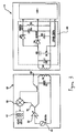
Referring to FIGS. 4 and 5, apparatus 110 for printing onto a base medium and data writing to a memory tag in or on the base medium is illustrated. This embodiment is for use with a base medium in the form of sheet paper 112, to which memory tags 108 have been applied or within which memory tags 108 have been embedded (as shown in FIG. 4). The memory tags 108 are RFID memory tags for which the manner of writing data to the tags and reading data from the tags is well known (see above, but in addition for example the RFID Handbook, Klaus Finkenzeller, 1999, John Wiley & Sons). For simplicity only those parts of the apparatus 110 which need to be shown to describe the invention are illustrated and described. It will be understood that the apparatus 110 includes much known technology from the prior art of printers, and from the prior art of RFID memory tags, which is not described here.
The apparatus 110 includes paper feed rollers 114 which are driven to rotate as indicated by arrows R1 to feed the paper sheets 112 through the apparatus 110 along a first axis in the direction indicated by arrows A1.
The apparatus 110 further includes a print head 116, which in this example is of ink jet form, mounted on a print head carriage 118 which extends across the apparatus 110 substantially perpendicular to the axis A1. The print head 116 is moveable back and forth along the print head carriage 118, in known manner. Thus the print head 116 is moveable back and forth along a second axis indicated by arrows A2, substantially perpendicular to the axis A1, to enable the print head 116 to access most of the upper surface 112 a of the paper sheet 112 as it moves through the apparatus 110, and thus to print anywhere on that accessible area of surface 112 a as required.
The apparatus 110 also includes a memory tag read/write device 120 which operates in known manner to write data to and/or read data from memory tags as required using an inductive coil 121. The inductive coil 121 of the memory tag read/write device 120 is connected to the print head 116 for movement back and forth along the print head carriage 118 with the print head 116. Thus the inductive coil 121 is moveable back and forth along a third axis indicated by arrows A3, substantially perpendicular to the axis A1, and parallel to the axis A2, to enable the memory tag read/write device 120 to read data from and/or write data to memory tags 108 located anywhere on or in the accessible area of the paper sheet 112, as will be described further below.
Referring now also to FIG. 6, the apparatus 110 also includes a main processor 122 and a mechanics controller 126, which controls all the mechanical operations of the apparatus 110, (i.e. the paper feed rollers 114, the movement of the print head 116 and inductive coil 121 along the print head carriage 118). The main processor 122 receives instruction signals from a host computer 124, including the details of:
what to print;
where to print it;
where the memory tag 108 is or tags 108 are in/on the paper sheet 112; and
what data to write to the memory tag(s) 108.
The main processor 122 sends command signals as required to:
the mechanics controller;
the print head 116; and
the memory tag read/write device 120,
to implement the instruction signals.
Thus the paper sheet 112 is fed through the apparatus 110 and has the required information printed on its upper surface 112 a. At the same time the memory tags 108 on or within the paper sheet 112 have the necessary data written to them by the memory tag read/write device 120, with the movement of the memory tag read/write device 120 (and print head 116) being paused with the memory tag read/write device 120 over the or each memory tag 108 as necessary for the data writing to take place.
The manner of co-ordination of the printing and data writing processes will depend on a number of factors. If, for example, the memory tags 108 are only present adjacent the top and/or bottom of the paper sheet 112 then the data writing process can take place before and/or after the printing. This would avoid the necessity for the printing process to be interrupted, and would make the co-ordination simpler. Further, when implemented with an inkjet printer, which in general requires a pause, after printing has been completed before the paper sheet is ejected, to allow the ink to dry, the data writing process could conveniently take place during this pause for memory tags present adjacent the bottom of the paper sheet 112.
In embodiments of the invention, the memory tags 108 will typically be read by hand held readers. Thus in order to assist users in the future to locate the memory tags 108 on the paper sheet 112 the memory tags 108 may have icons printed over their locations which can be readily identified by users. It is of course possible in the case of security documents that the location of memory tags 108 may not be advertised in this fashion, and that the position of memory tags may be concealed or multiple memory tags, some of which contain deceptive content, are provided, and that part of the authorisation information received by an authorised reader of the document is the knowledge of which memory tag 108 contains the valid information.
The memory tag read/write device 120 may, in addition to writing the data to the memory tags 108, also conduct a read operation to check that the data has written successfully before the paper sheet 112 is moved on following the data write operation. Alternatively, particularly if the apparatus 110 is operating at high speed, a separate data check device (not shown) may be included in the apparatus such that this operation takes place downstream of a memory tag write device which in this case need not also be capable of data reading.
It will be readily appreciated by the person skilled in the art that the modification to a conventional printing technology (in this case, the functional structure of the printing device is that customarily found in inkjet printing technology) can be employed to functional structures used in other printing technologies, such as laserjet and digital presses (such as HP Indigo presses). This last technology is particularly suitable for mass production of documents, for example book publication.
It can be seen from the above that there is no fundamental complexity involved in creating and publishing documents in accordance with embodiments of the invention using printing technology described in FIGS. 4 to 6. As for the content generation stage, conventional word processing and web publishing software (such as Microsoft Word and Microsoft Frontpage respectively) familiarly allows inserts of data of a different data type—in web publishing in particular, it is familiar to determine an icon for rendering that has a hyperlink function and can serve, if activated by a reader of the document, to link to another page or a file (such as a sound clip). Essentially the same approach can be taken here—the user composing the document on host computer 124 can place or identify a memory tag position on the page being composed and may designate a particular file to be stored in that memory tag. The document for printing, the files for the memory tags, and all placement information can then be provided by the document generation software on host computer 124 to the main processor 122 of the printing device for rendering as described above.
The security document contains at least two discrete forms of protection for the security information stored in the memory tag: protection against physical tampering, and protection against unauthorised reading. These will be considered in turn, together with any modification to the basic technology described above (in many cases it will be necessary for the physical isolation step to be completed after the document creation stages indicated above—in particular, to convert the memory tag to a read-only one, either by physically modifying the memory tag structure after writing or by preventing write access to the memory tag).
As the memory tag is both read and powered wirelessly, it is possible for it to be physically isolated (by encapsulation or otherwise). This physical isolation needs to be such that the memory tag can still be powered and read, and such that it can still be incorporated within or attached to the printed document. It is possible to protect the memory tag against the effects of physical tampering and still accept these constraints. Approaches to protection against tampering include using tamper-evident protection, and using tamper-resistant protection. Examples of each will now be described.
Tamper-evident protection does not itself prevent physical tampering. It does, however, show when physical tampering has occurred. For tamper-evident protection, it is necessary only that physical tampering will result in irreparable effects to the physical document that will be apparent on subsequent inspection. An example is the tamper-evident signature strip described in U.S. Pat. No. 5,762,378, in which the fabric of the tamper-evident area is weakened by a pattern of cuts through the paper substrate (illustrated in exemplary fashion in FIG. 7) in such a way that the cuts 701 through the paper substrate 702 in the tamper-evident area 703, which here also includes a memory tag 704, are such that attempts at physical modification within the tamper-evident area 703 will lead to irregular tearing patterns.
Tamper-resistant protection, by contrast, aims to prevent physical tampering. By “tamper-resistant”, it is not here implied that a tamper-resistant device is immune to all forms of tampering, however technically sophisticated. As is described in the literature of tamper protection (see, for example “Tamper Resistance—a Cautionary Note”, by Ross Anderson and Markus Kuhn, published in “The Second USENIX Workshop on Electronic Commerce Proceedings”, Oakland, Calif., Nov. 18-21, 1996, pp 1-11), most forms of tamper resistance can be overcome with sufficient time, money, and technical sophistication. Here, it is understood that protection is “tamper-resistant” if it is sufficient to increase significantly the level of difficulty for an attacker in achieving effective physical tampering.
As indicated above, a significant consideration in achieving effective tamper-resistant protection is that the ability to read data from the memory tag should be preserved. Full electromagnetic shielding of the memory tag—one known tamper-resistance technique—is thus not an option. A technique which may be an option, however, is effective design of the memory tag antenna. FIG. 8 shows an antenna structure for tamper protection. An antenna 801 on a Mylar sheet 802 is attached through an earth plane sheet 803 to the memory tag 804—the whole assembly being encapsulated and fixed on to the paper document (not shown). Advantageously, the memory tag in this arrangement may be written to, and then physically prevented from being rewritten, before the construction of the tamper-protected device. The meandering structure of the antenna (which may of course be a great deal more complex than shown here) has a secondary use as an inhibitor of the memory tag. A physical property of the antenna (such as its impedance, or time of flight along it) may be measured by the memory tag (which therefore will need to be provided with appropriate measurement circuits—the construction of which will be readily determinable by the skilled person) and compared with a known value. If this value is not returned, this will be taken as indicative of physical tampering (for example, the shorting together of two adjacent wires in the antenna) and the memory tag will not allow itself to be read by any reader.
Additional tamperproofing technologies, some but not all of which are applicable to the present use (again, this will be clearly evident to the person skilled in the art) are discussed in the applicants European Patent Application Publication No. 1273997. Again, for many of the techniques described here it will be desirable to write to the memory tag and to physically prevent further writing to the memory tag (or to a specific memory of the memory tag) before completing the tamperproofing process itself.
In addition to physical resistance to the effects of tampering, the memory tag itself provides security protection in that the information it holds is only usefully accessable to an authorised reader. This can be achieved in a number of ways, depending on factors such as the degree of security required, the length of time for which security is required, and the processing capacity (if any) available on the memory tag itself. Options, in ascending level of security, are described below.
(1) Pure Memory without Additional Security Features on Tag—all Security Operations Take Place Before Writing to Tag.
The security operations in this case take place on or before writing—for example, that the data stored in the memory tag is written with a secret. (For example, a hash function is used to take a hash over the picture of the holder, their access permissions, a reference to any credentials they produced when the badge was first created, and so on. The hash is authenticated using a secret shared among all authorised readers which could then be used (for example) as the access code in a keyed hash or MAC (Message Authentication Code). This may work very well in short term applications (eg entry to a specific event), but is less readily applicable to circumstances in which it is desired to write to the memory tag, particularly where it is necessary for the memory tag to contain updatable state information.
(2) Memory Tag with Unique ID
This provides substantial advantages for applications where writing to the memory tag is necessary. Each write to the memory tag which wishes to preserve integrity now incorporates the spot's unique ID in the hash which is MACed or signed; and each validator asks the spot afresh for its unique ID in recomputing the information-to-be-validated. This makes casual copying from one memory tag to another detectable, as the difference in unique IDs between the original and the clone will cause the hash comparison to fail.
There are a number of ways to create a unique ID. For maximum trackability, the format of a unique-ID may be (or is the unkeyed hash of) a manufacturer ID: week code: batch code: sequential number. An untrackable approach would be for the memory tag to contain a hardware-based random number generator (RNG), and upon first activation (maybe during manufacturing test) the RNG runs, the resulting unique-ID is written into write-once storage, and the writeability of that storage is reliably and permanently disabled. There's also a choice over how the unique ID is made accessible to the readers and writers: this can range from returning a raw ID to returning only a hash of a random number supplied by a reader with the unique ID. For random generation, to prevent clashes it would be desirable to have at least 256 bit unique Ids.
(3) Memory Tag with Unique ID, and On-Spot Hashing (with Some Access-Protected Storage)
This is the lowest security level which requires processing capacity on the memory tag. It is suitable for applications in which duplication of credentials must be detectable. It is particularly suitable where the memory tag should be relied upon to deliver results of processing over data it doesn't directly reveal, should be able to self-check the integrity of data it stores, or should be able to participate in providing confidentiality for data it stores.
Without its own processing, the memory tag needs to rely on the other components of a writing/reading/credentialing/validating system to hold all long-term and short-term secrets. A first cryptographic processing technology to employ in the tag itself is hashing, with SHA-1 being a logical choice of hash function. Hash functions are fast to execute, use relatively little RAM and code space, and are a building-block for reliable integrity checks.
One immediate use of an on-chip hashing capability is to hide the raw unique ID value from readers, instead of reporting the result of hashing that ID and a reader-supplied value. The use of that additional value would vary: it may be recorded alongside information recorded on memory tag, to allow a later recalculation of a hashed value; it may in other uses be a secret which is deliberately not recorded on the memory tag, allowing for a hash value recorded on the memory tag to be revalidated only by a validator which knows that secret value. An on-chip hashing function would also allow the memory tag to implement cryptographically-protected write-once storage, using a rolling hash of the data written into the “update-only” memory keyed with the unique ID so that the memory tag itself can report the integrity of the append-only log.
Using the hash function, it is possible to implement on-chip encryption. Briefly described, this can be done by hashing (a transform of) the unique ID and the starting address of a block of memory to create a pseudo-random stream which we XOR against the block of memory. What is stored is that encrypted form, while to read it out to a suitably-privileged reader (that would be a reader who can supply the extra secret needed for the transform of the unique ID) we recreate the keystream and XOR it against the stored data to derive plaintext.
Arrangements of this type allow for the possibility of access control: that areas of memory may be either encrypted or simply not returned to a reader unless that reader provides some suitable secret. The hash-derived keystream provides one way of doing that, with the chip returning contents of memory locations either as-they-are or XORed against a keystream determined by a combination of the unique ID and a reader-supplied quantity (a similar approach can be applied to writing). This still leaves the chip responding to all requests from all readers to read memory (with the notable exception of the uniqueID itself), relying on the result to be unintelligible without the correct key having been supplied. It may in some cases be advantageous to give the chip the capability of simply not responding to particular commands, and/or parameter values for some commands (for example, particular address ranges), unless the reader can supply an authentication value (or prove knowledge of an authentication value).
(4) Memory Tag with Unique ID On-Spot Hashing and Asymmetric Cryptographic Capability
This is appropriate where the memory tag has responsibility for control of data it stores, and can receive and transmit data with confidentiality and integrity. It is not apparent that many applications will require this approach to security, as the overall security of the system will generally be better improved by considering another aspect of the system (such as secure handling of authentication information provided to authorised readers).
Adding asymmetric cryptographic capability—RSA and elliptic-curve capability are both possibilities—to the spot has some notable costs: the codespace and memory requirements are non-trivial, the execution times for public-key operations are substantial (whole seconds), the management of key material and partial results becomes more complicated, and if the memory tags are expected to understand standard-format certificates too, the processing requirements go up some more. The advantage, though, is that we get a well-understood way of both validating data as having come from the memory tag, and sending it data which only it can read, without having to share the material for creating the validation and decrypting the data with any entity outside the memory tag (whether it's firmware in the reader/writer or code executing on a conventional host—PC, PDA, or similar).
(5) Memory Tag with Unique ID On-Spot Hashing, and Both Asymmetric and Symmetric Cryptographic Capability
This is useful where the memory tag is required to be a self-standing cryptographic object implementing a sophisticated information management policy. Again, the number of application scenarios where this will be appropriate may be rare. This is in part because the memory tag doesn't have human-interface capabilities of its own: so although it is now capable of doing symmetric cryptography as well as asymmetric, any bulk data it is handling still has to be passed, as plaintext, either into or out of the memory tag to interact with a person (be read, listened to, dictated in, or whatever). Thus, you have to trust the interaction device not to violate your security policy—i.e. to handle that valuable plain text resulting as securely as the highly secure memory tag.
A suitable processor for use in a memory tag to achieve functionalities as taught in sections (3) to (5) above is now described with reference to FIGS. 12 to 15. This processor is fully described in the present assignee's copending U.S. patent application Ser. No. 11/359,458 entitled “Memory Tags With Write Only Memory And Reader Devices And Methods Of Use Therefor”, filed on 23 Feb. 2006, which is incorporated by reference herein. A further memory tag processor design, not discussed further here but also suitable for achieving elements of the functionality described above, is described in the present assignee's copending U.S. patent application Ser. No. 11/294,479 entitled “Central Processor For Memory Tag”, filed on 6 Dec. 2005 and also incorporated by reference herein.
FIG. 12 shows schematically a memory tag reader and a memory tag suitable for use for embodiments of the present invention. In addition to the basic elements of a memory tag and reader discussed earlier, the following elements are also provided.
Firstly, the memory 102 of the memory tag is sub-divided into a number of memory types. There is an area of read-only memory (ROM) 108, an area of write only memory (WOM) 110, an area of system space 112 and an area of random access memory (RAM) 114. Each area of the memory 102 is controlled, in the preferred embodiment, by the memory controller 106 under the control of the device processor 104. The memory tag 100 in this case also incorporates a hash co processor 116—it will be appreciated that to achieve alternative security functionalities, alternative co-processor function may be provided.
The read-only memory 108 is a portion of memory which may, for example, be a single memory location, in which a global unique identification (GUID) that is assigned to the memory tag is stored. This global unique identification (GUID) is generally assigned to a tag upon its manufacture, that is it is stored in the ROM 108 when a tag is made. Alternatively, the global unique identification (GUID) may be written into the ROM 108 by the person/establishment, etc, issuing the tags prior to issuance. The area of ROM will then be locked such that it may no longer be modified.
The write-only memory 110 is an area of memory that is locked for the purposes of reading. This, for example, may consist of memory areas 2 to 31 (when the global unique identification is stored between memory addresses 0 and 1). This memory may only be written to by a write enabled reader device 200 accessing the memory tag. It may not be read. Should a memory tag reader device, such as device 200, attempt to read the memory addresses within the write-only section of memory 102, an erroneous response such as “0000” will be returned. The information stored at the memory addresses in question will not be provided to the reader device. Of course, the device processor 104 of the memory tag 100 is able to read the contents of the write-only memory 110 within the memory tag 100.
The system space 112 within the memory 102 is a portion of the memory 102 for use by the memory tag 100 itself in carrying out its operations. Finally, the random access memory 114 is an area of general storage within the memory tag. This area of the memory is utilised to store data on the memory tag, the purpose of memory tags, and is accessible by the reader device 200 for both reading and writing as required. Of course, this area of the memory tag memory 102 need not be non-volatile RAM. It may, for example, consist of non-volatile FLASH MEMORY or ROM.
The hash co-processor is a module within the memory tag 100 data stream which receives, via the device processor 104 and/or memory controller 106, a variable length input and performs a hash function upon that input. The output of the hash co-processor is therefore a fixed size bit stream known as a digest. Any cryptographically secure hash function may be used in the hash co-processor 116 of the present invention. For example, the hash functions MD5 or SHA1 may be utilised. However, in the preferred embodiment, an optimised version of SHA1 is run by hash co-processor 116. The SHA1 hash function is a secure hash function which receives a variable size stream of data (i.e. bytes) and produces a 160 bit digest in response to whatever data stream is supplied to it. Moreover, SHA1 is a one-way hash function, i.e. it is not possible to look at the digest produced by SHA1 and work backwards to find the data which was input to the function to produce the digest. SHA1 is particularly secure. It cannot be run backwards even to guess the last two or three digits of the input data sequence.
In its full implementation, 264 bits of data can be input to the SHA1 function before the digest produced by the function starts to repeat. SHA1 splits received data into blocks and processes one block at a time in order to produce the digest. However, in the optimised version which is preferably used in the hash co-processor 116 of the present invention, only one block, of 480 bits for example, is provided to the co-processor. This reduces significantly the time taken and power utilised to produce the digest.
It can be seen from FIG. 12 that the memory tag reader 200 also incorporates an area of write-only memory 204 and a hash co-processor 206. These elements have the same characteristics and operate in the same fashion as their counterparts in the memory tag 100. For example, the hash co-processor 206 will always employ the same hash function as the co-processor 116 in the memory tag. In fact, the hash co-processor 206 and the read-only memory 204 provided in the memory tag reader 200 may be provided in the form of a memory tag 100 operating as a co-processor within the reader device 200. However, in alternative memory tag reader devices there may be provided only the hash co-processor and write-only memory in addition to usual reader device functionality. All other functions may be provided through the reader device processor for example. This will prevent the presence of elements of a memory tag that are redundant when utilised as a co-processor in the memory tag reader 200.
The way in which the additional functionality described above with reference to FIG. 12 operates to provide a high confidence of the identity of a memory tag that is being read will now be discussed. Firstly, referring to FIG. 13, both a prior art data packet and a data packet utilised in authenticating a memory tag, for example, according to embodiments of the present invention, are shown. FIG. 13( i) shows a data packet which incorporates two synchronisation fields followed by a command field, an address field, a length field, a cyclic redundancy check field and a data field. In such a data packet, the command field will be populated with either a read or a write command. This packet structure may be used when performing a read or a write operation on a memory tag using a memory tag reader device, with write capability as necessary. However, a further command is required in order to enable an “authentication function” to be carried out. Accordingly, a data packet as shown in FIG. 13( ii) is required. Similarly to the prior art data packet, this data packet 300 incorporates two synchronisation data fields 302 and 304. These are followed by a command field 306. The command field may be populated with either a read command, a write command or an authenticate command. Where the command field is populated with an authenticate command, the next field in the data packet is a key address 308. This indicates the address at which key sequence data (as will be discussed in more detail below) commences within the write only memory area 110 of the memory tag 102. The key address field is followed by a random data length field 310, which specifies the length of the random data that will follow. Finally, a random data field is included in the data packet. The data in this field must be random as will be described later. The random data field is numbered 312 in FIG. 13 (ii).
In one suitable embodiment, the data packet which enables authentication omits a cyclic redundancy check-check sum data field. In this embodiment, the memory tag can be scanned many times by the memory tag reader device 200. However, in an alternative embodiment, a cyclic redundancy check data field may be included in the data packet. In this case, the memory tag reader will know, by virtue of the use of cyclic redundancy checking as is known in the art, that the packet was sent and received correctly, and the memory tag need only be scanned once by the memory tag reader 200. Hence, if the data returned to the reader device 200 from the memory tag 100 is incorrect, it is known as will be discussed below, without the need for further scans of the memory tag 100, that the memory tag 100 is not authentic.
The use of the architecture set forth in and with respect to FIGS. 12 and 13 will now be described with reference to FIG. 14, and utilising the example of a museum entry access system. A museum wishing to utilise memory tags to enable its patrons to gain access a given number of times will purchase, for example, a number of blank memory tags suitable for use according to embodiments of the invention. As is discussed further below, these may be incorporated into physical items in accordance with embodiments of the invention. As already discussed, these memory tags may have a global unique identification pre-assigned in the read only memory area of the memory tag. Alternatively, the read only memory area will be unlocked at delivery and blank to enable the museum to insert its own global unique identifier in the memory tags and to lock the read-only memory area once this is done. In a preferred embodiment, the global unique ID may be 1024 bits long.
In order for the entry access system to be effective, the museum must have what may be termed a “clean room” in which is located a memory tag read and write device 200. This device is the device utilised to issue key sequences to memory tags, i.e. to write a selected piece of data into the write-only memory area of each tag that is to be issued for use as a museum access device. The clean room is a room that is completely secure. Only authorised personnel are able to obtain access to that room and therefore only authorised personnel will know the key that is stored in the write-only memory area of issued memory tags.
The museum takes the blank tags which are purchased and, utilising the read and write device 200 within the clean room, writes one or more key sequences into the write-only memory area of these memory tags. Each tag is preferably provided with WOM sized to accommodate 2*16*240 bit key sequences, as are the reader devices. The memory tags are also configured to allow a predetermined number of accesses to the museum. The museum then issues these memory tags to museum patrons. When a patron wishes to gain access to the museum, for example, the memory tag is brought into close proximity to a memory tag reader device 200 that is present in the museum entry portal. Bringing the tag into close proximity causes it to be powered up and to interact with the reader as discussed above. Upon authentication of the tag and the data within the tag, access is granted.
Referring to FIG. 14, the process of determining whether a memory tag 100 presented to a memory tag reader 200 is authentic (in the example of the museum access tag given above, determining that the memory tag presented to the reader is a memory tag issued by the museum rather than a copy or clone thereof) is described. As already mentioned, when a memory tag is issued in the museum access example given above, a key sequence which is known only to certain museum personnel is written into the write only memory area of the memory tag. At the same time, the same key is written into the write-only memory area 204 in each memory reader device 200 that is to be employed to read that tag 100. For the purposes of this example, the key sequence will be represented by the sequence “ABC”, but the key sequence may be any combination of letters and/or numbers and/or symbols. This is a secret key sequence known only to the personnel who operate the clean room in the museum and it cannot be read from the write only memory area 110 in the memory tag 100 other than by the memory tag device processor 104. Similarly, it cannot be read from the write only memory area 204 in the memory tag reader other than by the memory tag reader device 200 processor. Of course, the key may be used in any number of memory tags 100.
When a patron of the museum arrives at the museum portal and wishes to gain access, the memory tag 100 is presented to the reader 200 on the door, as already discussed. In order to authenticate the tag as a tag issued by the museum, the reader device 200 on the door of the museum sends an authentication data packet, as shown in FIG. 13 to the memory tag 100. Upon receiving an authentication command, the device processor 104 within the memory tag 100 makes use of the memory controller 106 and accesses the data specified by the key address field 308 in the data packet 300 received from the reader device 200. The device processor 104 therefore reads, in this example, the sequence “ABC” from the write only memory area 110. This step is set forth in function box 402 of FIG. 14. The memory tag 100 has also received, by way of data field 312 in data packet 300, an amount of random data. This random data is combined with the key sequence “ABC” (function box 404). The key sequence and random data may be combined in any suitable fashion. However, in a preferred embodiment, the key sequence data and random data are interleaved.
At this point it is to be mentioned that the random data is provided to the memory tag 100 from the memory reader 200. The reader device functionality 202 is provided with a random number generator. It is necessary to use random data in order to prevent what is termed “the man in the middle attack”. This will be described in more detail below.
The combined key sequence and random data is then passed, in the memory tag 100, under control of the device processor 104 to the hash co-processor 116. The hash co-processor performs a hash function, in the preferred embodiment an optimised SHA1 function, on the data passed to it and produces a hash digest (function box 406). The hash digest is then passed under the control of the device processor 104, via the inductive link, to the memory tag reader 200. As already noted, the hash digest is, in the preferred embodiment, a 160 bit SHA1 digest.
Whilst the above operations are being performed in the memory tag 100, the following steps are carried out within the memory tag reader device 200. The following steps are carried out either under the control of the reader device functionality in one embodiment, or under the control of the device processor and memory controller of the memory tag that is utilised in the memory tag reader device 200 as a co-processor. In the latter scenario, the device processor of the memory tag is operated under the control of the reader device functionality, which includes the reader device processor.
Firstly, the key sequence, in this example “ABC”, is read from the write only memory area 204 in the memory tag reader 200. This sequence is identified by the key address value which is also provided to the memory tag (function box 408). The memory tag reader device 200 also retains within it a copy of the random data which is forwarded to the memory tag 100 in random data field 312 of data packet 300. This random data is combined, in the same way as in the memory tag 100, with the key sequence that has been read from the write only memory area 204 within the memory tag reader 200 (function box 410). This combination of data is then passed through the hash co-processor 206 within memory tag reader 200, which is identical to that in memory tag 100 and which therefore will provide an identical digest as long as the key stored in the memory tag reader is identical to the key stored in the memory tag 100 (function box 412).
The memory tag reader device 200 and thus the memory tag reader device processor is now in possession of the hash digest produced in the memory tag 100 and the hash digest produced in the memory tag reader 200. These are compared (function box 414, 416) and if they match the memory tag is identified as authentic (function 418). Otherwise, the memory tag is not an authentic tag and may be rejected (function box 420).
As will be appreciated, this process of authentication prevents the copying or cloning of memory tags. The write only memory area of the memory tag cannot be read by a memory tag reader device, such as device 200, and therefore cannot be written into a second memory tag. Therefore, if a memory tag is cloned, upon carrying out the authentication process described above, the hash digest produced in the memory tag will be different to that produced in the memory tag reader, because the key sequence “ABC” will not be present in the memory tag. This will result in the memory tag being identified as not authentic.
This authentication procedure also prevents the man in the middle attack, as mentioned above. The man in the middle attack is as follows. A device placed between a reader and a tag will read the output of a tag when it is queried by a reader device. Thereafter, every time the tag is read, the “man in the middle” device will send to the reader that first output. That is, the man in the middle looks at the hash digest that is produced by the memory tag and sends it to the reader. Thereafter, whenever the tag is read, the man in the middle returns the same hash digest. If deterministic data is combined with the key sequence it is possible to determine what the key stored in the tag is by looking at various digests sent by the tag. This is not possible if random data is used as in the present invention.
In order to make the above process more secure, the global unique identification (GUID) assigned to a memory tag may be read from the ROM area of the tag 100 and combined with the chosen key sequence. This combination may then be passed through a hash co-processor and the digest produced may be stored as the key sequence in the WOM areas in the memory tag and the memory tag reader. Doing this ties the key sequence to the memory tag and therefore gives more security. Again, the combination of the global unique identification and the chosen sequence may be performed in any way, such as interleaving.
It is also possible to authenticate the data that is stored in the random access memory area 114 of a memory tag 100 memory 102. This procedure requires the use of a further key sequence which is also stored in the write only memory of the memory tag. This is discussed with reference to FIG. 15.
As before, the person or institution issuing memory tags chooses a key sequence, which will be “ABC” again in this example. This is stored as the first key value in the write only memory 110 of a memory tag 100 and also in a write only memory 204 of a memory tag reader 200 as described above. This sequence is only known to the person/institution issuing the memory tags. Other data, which is readable by the memory tag reader device 200, is stored in the random access memory area 114 in the memory tag 100. In the example of museum access, this may be a number of entries that are permitted to the museum, for example 20. The data stored in the random access memory area 114 is also combined with the first key sequence (in any suitable fashion, but preferably by interleaving) and that combination is then passed through a hash co-processor, either in the memory tag 100 or in the memory tag reader 200, when the key sequences are written. This hash digest is then stored as the second key sequence in the write only memory area 110 of memory tag 100 only.
In order to authenticate that the data stored in the random access memory area 114 of the memory tag 100 is correct, and has not, for example, been tampered with by someone wishing to increase their number of allowed accesses, the following steps are carried out.
When the memory tag is brought into close proximity with the memory tag reader at the museum portal the procedure set forth above is carried out in order to permit interaction between the two devices. The reader device 200 then sends to the memory tag 100 a normal read request in order to read from the random access memory area 114 the data that is stored in it. Upon receipt of this read request, which may for example take the form of a data packet such as that shown in FIG. 1 b(i), the memory tag device processor 104 activates the memory controller 106 and reads from the random access memory area 114 the data stored therein, in this example the value “20”. That data is then passed, via the inductive link, to the memory tag reader 200 (function box 502). It should be appreciated that the data stored in the random access memory (RAM) area 114 of the memory may be accessed and altered by unauthorised personnel, in this example to increase the permitted number of accesses to the museum. Such behaviour will however be detected, as discussed below.
The reader device 200 then sends to the memory tag 100 a data packet including an authenticate command and the address of the second key sequence along with random data. In response to this, the memory tag 100 reads the second key sequence from the specified memory location in the area of WOM 110 (function box 504) and combines the second key sequence with the random data (function box 506). This combination is carried out in any suitable manner, but again interleaving is preferred.
This data sequence is then passed through the hash co-processor which produces a hash digest, in the preferred embodiment an optimised SHA1 digest of 160 bits in length (function box 508). The hash digest is then passed, via the inductive link and under the control of the memory tag device processor 104, to the tag reader device 200.
Meanwhile, in the memory tag reader 200, the key sequence “ABC” stored in the write only memory area 204 within the memory tag reader device 200 is read in the same fashion as described above with regard to FIG. 15 (function box 510). This key sequence is combined with the value read from the random access memory area 114 of the memory tag 100 (function box 512). A hash digest of the combination is generated in the reader device. This hash digest is then combined with the random data that was forwarded to the memory tag, which is also forwarded to the relevant module within the reader device functionality 202 (function box 514).
The final combination of data produced in function box 514 is then passed through the hash co-processor 206 in the memory tag reader 200, which operates as described previously to generate a hash digest (function box 516). This hash digest is compared by the memory tag reader device processor with the hash digest received from the memory tag (function 518).
As will now be apparent, the hash digest produced in the memory tag is produced from the combination of the second key value with random data. The hash digest generated in the reader device 200 is generated from a hash digest (generated from the first key value combined with the data stored in the random access memory area 114 of the memory tag) combined with random data in the same manner as in the memory tag before being hashed. As the second key sequence in the memory tag 100 corresponds to the hash digest of the first key sequence combined with the data stored in the random access memory area 114, if the data stored in the random access memory 114 is tampered with, the hash digest generated in the reader will be different to that generated in the memory tag. Hence, if the digests match (function box 520), the data stored in the random access memory area 114 is authentic (function box 522). However, if the digests do not match, the data stored in the random access memory 114 is not authentic, and has therefore been tampered with or the like (function box 524). Hence, the authenticity of any data stored in the area of general access memory (RAM 114) may be assured.
In the example of museum access, therefore, once the data stored in the random access memory area 114 has been authenticated, the portal can allow access to the museum and the reader device 200 can i) write a decremented value into the random access memory area, and ii) generate a hash digest of the new data combined with the first key sequence and write this to the second key sequence location in the write only memory. One of the permitted entries to the museum is therefore wiped from the memory tag access device. Such a process may be utilised equally in bus/train passes and telephone payment cards for example. It may also be used in payment cards for other services and/or items, for example.
Of course, the process of FIG. 14 and the process of FIG. 15 may be carried out on the same memory tag. Hence, the authenticity of a memory tag may be ascertained utilising a first key sequence and the authenticity of the data stored upon the memory tag may be ascertained utilising the first key sequence, a second key sequence and the data stored in the random access memory area 114. Moreover, more than one key sequence (present in both the memory tag and the reader device areas of WOM) may be combined and then be combined with the random data in either of the above examples, thereby providing greater security.
Using the approaches described above, a security document can be created which comprises a printed document and one or more memory tags. These memory tags are memory circuits adapted to be read wirelessly (preferably, inductively powered also) and are attached to or incorporated within the printed document. Data in the memory circuit is protected from access by an unauthorised reader, either by measures taken in writing the data, or by presence of a unique ID or cryptographic capacity in the memory tag itself. The memory tag is physically isolated so as to inhibit physical tampering (for example, by tamper-resistant techniques of the kind discussed with reference to FIG. 8) or to indicate when physical tampering has occurred (for example, by tamper-evident techniques of the kind discussed with reference to FIG. 7).
The steps involved in creation of such a document are illustrated in FIG. 10. A first step 1001 is to determine some information for printing in a printed document, and further information for writing to the memory physically located in the document. Where the document is a bearer document (such as a passport or bank passbook), the printed information may include a photograph, a signature, a name or other biographical or practical details, whereas the stored information may provide similar information but most effectively will contain information which is complementary rather than identical (it may, for example, be particularly useful for bearer image information to be stored only in the memory, so that it is not visually apparent from the document on its own). A next step is to protect 1002 the memory information from unauthorised reading by one of the methods discussed above. After this, the relevant information is printed 1003 to the printed document, and the protected information written 1004 to a memory circuit, with the memory circuit being incorporated 1005 into the document such that it can be read wirelessly but in a physically isolated manner such that physical tampering is inhibited or made detectable.
A security document of this type is shown in FIG. 9, which also illustrates how a document of this type would be read, with reference to FIG. 11. A security document 901 contains printed material and a signature strip 902, signed by an authorised bearer. Embedded within the security document 901 is a memory tag 903 embedded in a tamper-resistant region 903. A reader for the memory tag comprises a stylus 910 used in conjunction with a computer or other processing device 911—the processing device has a display 912.
The reader may now, or later, be equipped 1101 with authorisation information enabling it to interpret or obtain information received from the memory tag. While a user views 1102 printed information, the reader accesses 1103 the memory tag 903 to obtain information from it. The physical isolation and protection of the memory tag, together with the security policy employed in writing to or electronically protecting the memory tag, should be sufficient to give adequate confidence to the authorised reader that the memory tag has not been subverted. The information in the memory tag is then downloaded, after whatever security interchange between the memory tag processor (if there is one) and the processor 911 is required, and decrypted or otherwise converted 1104 to usable form by use of the authorisation information, to which processor 911 has access. The results are then displayed on display 912. In this case, what is displayed is the signature matching the signature on the signature strip 902, but also the face of an authorised bearer—the user of the reading device can therefore use 1105 these complementary pieces of information to determine not only whether the security document is valid (by the matching of the signatures) but also whether it is being carried by the correct person—this information not being available to an unauthorised bearer, as the security document itself contains no printed picture.
Such a security document could be used, as in the scenario described above, identify an authorised bearer of the security document. However, it could also be used to allow access to a specified asset or assets by the authorised bearer (such as a bank account). A part of this process could be to update state information (such as a withdrawal log) on the memory tag itself, for a memory tag which contains writable memory.
A further approach to providing a physical item according to embodiments of the invention is discussed with reference to FIG. 16 onwards. In this approach, data hidden by combination with other elements on the physical device is shown to enable an exemplary authentication solution. This uses steganographic techniques—steganography is the discipline of writing hidden messages in such a way that no one apart from the intended recipient knows of the existence of the message; this is in contrast to cryptography, which involves obscuring the content of messages which are known to exist. The example shown uses a combination of steganographic, cryptographic and biometric techniques to provide an effective method of secure authentication without connection to an authorization server.
FIG. 16 shows an exemplary physical item according to this embodiment of the invention. It is here in the form of a card 1601, with images 1602, 1603 and text 1604, and a memory tag 1605. The memory tag 1605 is adapted to store user biometric data, the biometric data itself containing further data hidden steganographically. A process for creating such a card 1601 will now be described with reference to FIG. 17. It should however be noted that the physical item need not be a card as shown here—it could be any physical object to be held personal to a user (such as a key tag, charm, pen, watch, locket or even a mobile phone).
Creation and initialization of the card 1601 involves use of one or more servers (for example, a suitably configured authorization server 1702). Various inputs 1701 to the process are required, all of which need to be supplied to at least one of the server side blocks required for the creation and initialization process. The system has a number of outputs 1703 to be provided either in the card 1601 (image or memory spot), or to the user associated with the card 1601. The different elements of creation and initialization of the card by server 1702 will be discussed in turn.
Block 1710 involves the generation or selection of encryption and decryption keys. This may be done by standard cryptographic techniques, with number of bits of encryption and mechanism selection (for example, symmetric or asymmetric) chosen on the basis of degree of security required against convenience and processing power available. The encryption key 1711 will be used further by the server 1702. The decryption key is in this arrangement split into two parts, which may be done in any conventional way. A first part 1713 is to be provided by the user, as a user PIN (or as part of a user PIN). A second part 1714 is to be used to form part of the steganographically hidden data, and so provides an input to a later server side block. This ensures that user input is required when the memory tag is read from the subsequently produced card to allow the hidden data to be decrypted.
Block 1720 involves the encryption of data to be held steganographically. This involves three of the inputs 1701. The first of these inputs is a unique memory tag ID 1721. As indicated previously, a unique memory tag ID has the desirable effect of preventing the cloning of a physical item containing a memory tag by simply copying data to a different memory tag. The second of these inputs is data 1722 relating to a resource to be accessed by a user—for example, an indication of user privileges, or time limits for valid authorisation. The third of these inputs is data 1723 private to the user (such as medical or other private data which the user would only wish to release to known other parties). For some purposes, the second input or the third input may not be required. These three inputs are combined together in any appropriate manner to form combined data 1724, which is encrypted by the encryption block 1720 using the encryption key 1711. The encryption key 1711 may be destroyed at this point to prevent replication of the encryption procedure should the key be subsequently found. The encrypted data 1725 resulting is then added to the second part 1714 of the decryption key (further unencrypted data may be added at this point, for example to present an appropriate message to the successful decrypter of the message or to round the data to a uniform size) to form the data 1726 for hiding.
Block 1730 involves the generation or selection of a key (termed a “stego key”) for the hiding of data steganographically. This key—which may be any kind of key conventionally used for the purpose—should be disclosed to the relevant user. This key is, preferably, one that can be memorized by the user—though secure storage personal to the user may provide an alternative.
Block 1740 involves the creation of the steganographically hidden data. This requires a further input from the user in the form of user biometric data 1741. This could be effectively any form of biometric data—fingerprint, iris scan, high resolution image, voice sample, even DNA—in digital form. This biometric data is preferably of high quality—not only is this in itself desirable for authentication, but it also provides for additional bits of resolution which can readily be used to hide data. This and the stego key 1731 are provided as inputs to a steganographic algorithm—which, again, may be of any conventional type (examples are discussed in “Information Hiding Techniques for Steganography and Digital Watermarking”, edited by S. Katzenbeisser and F. A. P. Petitcolas, Artech House, 2000). The result is “stego-object” 1742, which comprises user biometric data 1741 with the data for hiding 1726 steganographically hidden within. This stego-object 1742 is to be written to the memory of the memory tag of the card 1601.
The stego-object 1742 written to the memory of the memory tag is desirably written into memory which can only be written once but read many times. Such a function may be achieved physically (by burning out one or more switches on the memory tag after writing data) or in software.
The process of authentication of a user to an appropriate third party is shown in FIG. 18. It can be noted that this authentication process does not rely on the active presence of any authentication server—all such interactions take place only during initialization, rendering this approach to authentication particularly effective where there will not always be a network (or perhaps a trustworthy network) present. It will be shown that the arrangement described will satisfy the basic principles of authentication processes—it establishes who you are, what you have, and what you know.
The three entities interacting in the authentication process shown in FIG. 18 are the memory tag 1801 embedded in the physical item, the memory tag reader 1802 of the third party, and the user 1803 who is associated with the physical item. The memory tag 1801 contains the stego-object 1804, which has within it both biometric data 1811 and the hidden data 1821, and the memory tag unique ID 1805. The memory tag reader 1802 has the relevant software for validation and decryption of data, but has no input data. The other input data not provided at the memory tag 1801 is provided by the user 1803.
The first step 1810 is the extraction of biometric data. This involves the collection of biometric data 1812 from the user 1803 and uploading of the biometric data 1811 from the memory tag 1801. The complexity of this procedure may depend on the degree of security required and the appropriateness of a credential to a particular purpose. For example, an appropriate solution may be for the biometric data 1811 on the memory tag to be an image of the user (for security purposes, it may be desirable for this image not to be identical to any user image printed on to the physical item itself). The “validator” 1810 for this biometric data may simply be a display function at the memory tag reader 1802 to allow the third party controlling the user to compare the image data 1811 stored on the tag with the user's actual appearance 1812. If different biometric data is desired—for example user fingerprints—then the biometric data 1811 stored on the memory tag 1801 may need to be compared with data 1812 measured from the user 1801 with an appropriate measurement function of, or associated with, the memory tag reader 1802 (such as a fingerprint reader) and then compared by an appropriate comparison program within the biometric data validation block 1810. The stored biometric data 1811 should not need to be separated from the hidden data 1821 to be evaluated—while it is the biometric data 1811 that is being in effect compared, any comparison operation performed by the validation block 1810 is in fact carried out on the whole stego-object 1804. It is therefore desirable for the biometric data to be of sufficiently high resolution that the very highest data resolution is not necessary for validation (so this level of resolution can be “corrupted” by hidden data).
If this biometric check fails, the whole process fails 1860—typically this will mean that the user is not allowed access to resources controlled by the third party controlling the memory spot reader 1802. If the biometric check succeeds, the control passes to the next functional, the steganographic extractor (SE) block 1820. This block contains a steganographic algorithm for data extraction (matching the steganographic algorithm used for hiding the hidden data). As indicated previously, any appropriate existing steganographic method may be used for this purpose. It is desirable for the steganographic algorithm to be “non-robust”, meaning that it is sensitive to relatively minor changes to the “hiding” data—in this case, the biometric data. This is advantageous as even minor tampering to the biometric data will affect the steganographically hidden data—this can be reinforced by including a digest (for example, a hash such as that produced by one of the SHA algorithms) of the original biometric data in the hidden data. The steganographic algorithm requires an input from the user—this is the stego password 1822 produced before the hiding algorithm was run in the initialization phase and provided to the user at that time. Successful extraction of the hidden data is only possible with this password—if it is not provided, then (depending on the algorithm used) there may be either no data produced at all by running the algorithm, or only garbage data. Assuming successful recovery, the extracted hidden data 1830 will comprise some encrypted data (as discussed below), a partial decryption key and a message digest or other information related to the original biometric data—if the data takes this form, it is possible to move to the next functional block, whereas if it does not, authentication fails 1860.
The final stage 1840 is the decryption of the encrypted data contained in the extracted hidden data 1830. While part of the password for decryption is provided with the hidden data 1830, the other part 1823 is in the possession of the user 1803 and must be supplied by them. The two parts of the decryption key are then combined (in whatever way they were previously separated—this may simply be by having the first half of the bits assigned to the hidden data and the second half assigned to the user, for example) and the full decryption key used to decrypt the encrypted data according to the appropriate encryption algorithm. The resulting plain data may contain information relating to the rights allowed to the user 803 in respect of the resources to which the user is requesting access from the third party controlling the memory tag reader 802—these may include an authorization to use a particular resource, explanatory information from resource owners, access time limits, or user personal information, for example. As a final defence against cloning, the plain data also contains the memory tag unique ID which can be compared directly against the memory tag ID 1805 uploaded from the memory tag 1801. If the unique IDs match, that confirms that the stego object 1804 has not been copied from one memory tag to another in a cloning attack. If the tag IDs match and the data is of an allowable type, access to the desired resource or resources is granted 1870—if this stage fails, access is denied 1860.
This approach allows for effective authentication even without an authorisation server (or network connection). It defends against alteration of the biometric data in that such alteration will compromise the hidden data. It defends against data modification as reinsertion of data requires knowledge of relevant algorithms and encryption keys, and as the memory tag stores (in preferred embodiments) such data in a write-once memory. Memory spot unique ID provides a defence against cloning.
It can thus be seen that the integration of a memory tag into a physical item may be used very effectively to provide authentication solutions, particularly solutions that do not rely on the presence of other networked components such as an authorization server.

Claims (12)

1. A physical object, comprising one or more memory circuits attached to or incorporated within the physical object that are wirelessly readable by a reader device, wherein data in the memory circuit is protected from access by an unauthorized reader, wherein data in the memory circuit identifies an authorized bearer of the physical object, and wherein data in the memory circuit allows access to a specified asset or assets by the authorized bearer,
wherein the memory circuit contains biometric data of the authorized bearer and further authorization data steganographically hidden in the biometric data of the authorized bearer,
wherein the further authorization data comprises encrypted data and a part of a decryption key for the encrypted data,
wherein the encrypted data includes information relating to the specified asset or assets and the authorized bearers entitlement to access to it or them, and
wherein the part of the decryption key is combinable with a bearer provided part of the decryption key to form a decryption key for decryption of the encrypted data.
2. A physical object as claimed in claim 1, wherein the memory circuit is inductively powered.
3. A physical object as claimed in claim 2, wherein the memory circuit receives and transmits data wirelessly at radio frequency.
4. A physical object as claimed in claim 1, wherein the memory circuit is physically isolated so as to inhibit physical tampering or to indicate when physical tampering has occurred.
5. A physical object as claimed in claim 1, wherein the memory circuit comprises a read only memory holding a unique ID for the memory circuit.
6. A physical object as claimed in claim 1, wherein the memory circuit comprises a processor operable to process received data and to generate data to be transmitted to the reader device.
7. A physical object as claimed in claim 6, wherein the memory circuit further comprises an area of write-only memory which may be written to by a suitable memory tag reader device but which may be read only by the processor of the memory circuit.
8. A physical object as claimed in claim 7, wherein the memory circuit further comprises a hash co-processor configured to apply a cryptographically secure hash function to data input to it.
9. A physical object as claimed in claim 1, wherein the encrypted data includes information relating to the specified asset or assets and the authorized bearers entitlement to access to it or them.
10. A physical object as claimed in claim 1, wherein the memory circuit comprises a read only memory holding a unique ID for the memory circuit, and wherein the encrypted data also contains the unique ID for the memory circuit.
11. A method of providing a physical object for an authorized bearer to allow access to a specified asset or assets by the authorized bearer, comprising:
a. generating an encryption key and a decryption key, and dividing the decryption key into a first part and a second part;
b. encrypting data relating to the specified asset or assets and a unique ID of a memory circuit to form encrypted data, and combining the encrypted data with the second part of the decryption key to form data for hiding;
c. generating a steganographic key; and
d. obtaining biometric data of the authorized bearer, and using the steganographic key and a steganographic algorithm to create a steganographic data object in which the data for hiding is hidden in the biometric data of the authorized bearer; and
e. writing the steganographic data object into the memory circuit whose unique ID is included in the encrypted data,
wherein a decryption key for decrypting the encrypted data is formed by combining the first part of the decryption key which is provided by the bearer with the second part of the decryption key which is included in the data for hiding.
12. A method of authenticating a bearer of a physical object as an authorized bearer entitled to access to a specified asset or assets, comprising:
a. obtaining biometric data from the bearer and comparing the obtained biometric data with biometric data stored in a memory circuit of the physical object;
b. if the obtained biometric data matches the stored biometric data, extracting data hidden steganographically in the stored biometric data by use of a steganographic key provided by the bearer;
c. if the data hidden steganographically has an expected form and comprises encrypted data and a second part of a decryption key, decrypting the encrypted data by use of a decryption key formed by combining the second part of the decryption key and a first part of the decryption key which is provided by the bearer; and
d. if the decrypted data has an expected form, allowing the bearer access to the specified asset or assets as the authorized bearer of the physical object.
US11/493,031 2003-01-15 2006-07-26 Physical items for holding data securely, and methods and apparatus for publishing and reading them Active 2026-03-14 US7712675B2 (en)

Priority Applications (1)

Application Number Priority Date Filing Date Title
US11/493,031 US7712675B2 (en) 2003-01-15 2006-07-26 Physical items for holding data securely, and methods and apparatus for publishing and reading them

Applications Claiming Priority (4)

Application Number Priority Date Filing Date Title
GB0300906.5 2003-01-15
GB0300906A GB2397272B (en) 2003-01-15 2003-01-15 Secure physical documents and methods and apparatus for publishing and reading them
US10/697,272 US7309017B2 (en) 2003-01-15 2003-10-31 Secure physical documents, and methods and apparatus for publishing and reading them
US11/493,031 US7712675B2 (en) 2003-01-15 2006-07-26 Physical items for holding data securely, and methods and apparatus for publishing and reading them

Related Parent Applications (1)

Application Number Title Priority Date Filing Date
US10/697,272 Continuation-In-Part US7309017B2 (en) 2003-01-15 2003-10-31 Secure physical documents, and methods and apparatus for publishing and reading them

Publications (2)

Publication Number Publication Date
US20070095928A1 US20070095928A1 (en) 2007-05-03
US7712675B2 true US7712675B2 (en) 2010-05-11

Family

ID=40265973

Family Applications (1)

Application Number Title Priority Date Filing Date
US11/493,031 Active 2026-03-14 US7712675B2 (en) 2003-01-15 2006-07-26 Physical items for holding data securely, and methods and apparatus for publishing and reading them

Country Status (1)

Country Link
US (1) US7712675B2 (en)

Cited By (14)

* Cited by examiner, † Cited by third party
Publication number Priority date Publication date Assignee Title
US20050207823A1 (en) * 2004-03-20 2005-09-22 Hewlett-Packard Development Co., L.P. Digital pen and a method of storing digital records of the use made of the digital pen
US20070036470A1 (en) * 2005-08-12 2007-02-15 Ricoh Company, Ltd. Techniques for generating and using a fingerprint for an article
US20070233612A1 (en) * 2006-03-31 2007-10-04 Ricoh Company, Ltd. Techniques for generating a media key
US20070233613A1 (en) * 2006-03-31 2007-10-04 Ricoh Company, Ltd. Techniques for using media keys
US20070230703A1 (en) * 2006-03-31 2007-10-04 Ricoh Company, Ltd. Transmission of media keys
US20070234215A1 (en) * 2006-03-31 2007-10-04 Ricoh Company, Ltd. User interface for creating and using media keys
US20080244721A1 (en) * 2007-03-30 2008-10-02 Ricoh Company, Ltd. Techniques for Sharing Data
US20080243702A1 (en) * 2007-03-30 2008-10-02 Ricoh Company, Ltd. Tokens Usable in Value-Based Transactions
US20080240816A1 (en) * 2007-03-30 2008-10-02 Ricoh Company, Ltd. Pre-Scanning Printer with Paper Fingerprinting
US20090240955A1 (en) * 2006-05-31 2009-09-24 Datamark Technologies Pte Ltd. Secure media storage device and method of securing media storage devices
US20100102966A1 (en) * 2008-10-27 2010-04-29 First Data Corporation Devices and Methods for Protecting a Packaged Radio Frequency Identification Device from Electronic Reading
US20150242608A1 (en) * 2014-02-21 2015-08-27 Samsung Electronics Co., Ltd. Controlling input/output devices
US9460688B2 (en) 2014-06-16 2016-10-04 Rod G. Kosann Electronic display locket and system
US9721127B2 (en) 2014-03-10 2017-08-01 The Raymond Corporation Systems and methods for controlling activation of options preloaded on a material handling vehicle

Families Citing this family (26)

* Cited by examiner, † Cited by third party
Publication number Priority date Publication date Assignee Title
GB2397272B (en) * 2003-01-15 2006-11-15 Hewlett Packard Co Secure physical documents and methods and apparatus for publishing and reading them
US7712675B2 (en) * 2003-01-15 2010-05-11 Hewlett-Packard Development Company, L.P. Physical items for holding data securely, and methods and apparatus for publishing and reading them
US7246754B2 (en) * 2004-02-18 2007-07-24 Hewlett-Packard Development Company, L.P. Secure currency
JP4208776B2 (en) * 2004-06-25 2009-01-14 キヤノン株式会社 Print client, network printer and printing system
US20080230615A1 (en) * 2007-03-19 2008-09-25 Sony Corporation Near-field communication card for communication of contact information
WO2009079734A1 (en) * 2007-12-20 2009-07-02 Bce Inc. Contact-less tag with signature, and applications thereof
WO2009130086A1 (en) * 2008-04-22 2009-10-29 Siemens Aktiengesellschaft Method and device for providing compatible data
US8098825B2 (en) * 2008-06-30 2012-01-17 Condel International Technologies Inc. Method and system for enhancing data encryption using multiple-key lists
US8009831B2 (en) * 2008-06-30 2011-08-30 Condel International Technologies Inc. Method and system for hiding the decryption key in a dispersive way
JP4548524B2 (en) 2008-07-29 2010-09-22 ソニー株式会社 COMMUNICATION DEVICE, PROGRAM, COMMUNICATION METHOD, AND COMMUNICATION SYSTEM
TWI451740B (en) * 2008-09-24 2014-09-01 Shrisinha Technology Corp Hardware Password Verification Method and Its System
TWI400925B (en) * 2008-11-12 2013-07-01 Condel Internat Technologies Inc Method and system for enhancing data encryption using multiple-key lists
CA2747553C (en) 2008-12-18 2016-06-07 Sean Maclean Murray Validation method and system for use in securing nomadic electronic transactions
US20120102322A1 (en) 2008-12-18 2012-04-26 O'brien William G Processing of communication device signatures for use in securing nomadic electronic transactions
EP2237519A1 (en) * 2009-03-31 2010-10-06 France Telecom Method and system for securely linking digital user's data to an NFC application running on a terminal
US8547232B2 (en) 2010-05-28 2013-10-01 Nokia Corporation Method and apparatus for transferring data via radio frequency (RF) memory tags
AU2012371253A1 (en) * 2012-03-01 2014-09-18 Siemens Aktiengesellschaft RFID transponder having a plurality of memory areas
US9128811B2 (en) * 2012-06-26 2015-09-08 Intel Corporation Assigning addresses to devices on an interconnect
DE102013222273A1 (en) * 2013-11-01 2015-05-07 Bundesdruckerei Gmbh reader
EP2930663B1 (en) * 2014-04-11 2020-07-01 Nxp B.V. Electronic circuit chip for an RFID tag with a read-only-once functionality
WO2020162898A1 (en) 2019-02-06 2020-08-13 Hewlett-Packard Development Company, L.P. Identifying random bits in control data packets
MX2021008854A (en) 2019-02-06 2021-09-08 Hewlett Packard Development Co Integrated circuit with address drivers for fluidic die.
WO2020162894A1 (en) * 2019-02-06 2020-08-13 Hewlett-Packard Development Company, L.P. Data packets comprising random numbers for controlling fluid dispensing devices
PL3717247T3 (en) 2019-02-06 2021-11-29 Hewlett-Packard Development Company, L.P. Print component with memory array using intermittent clock signal
US20220164806A1 (en) * 2019-04-16 2022-05-26 Stegvision Corp. Product authentication systems, methods, and devices
US10691938B1 (en) * 2019-09-30 2020-06-23 Capital One Services, Llc Systems and methods for authenticating a stack of cards

Citations (97)

* Cited by examiner, † Cited by third party
Publication number Priority date Publication date Assignee Title
US5055913A (en) 1986-11-20 1991-10-08 Gao Gesellschaft Fur Automation Und Organisation Mbh Terminal arrangement for integrated circuit device
US5090736A (en) 1991-01-28 1992-02-25 Transilwrap Company, Inc. Multi-sheet laminated identification card with tamper resistant, ultrasonic weldments
US5469506A (en) * 1994-06-27 1995-11-21 Pitney Bowes Inc. Apparatus for verifying an identification card and identifying a person by means of a biometric characteristic
US5590038A (en) * 1994-06-20 1996-12-31 Pitroda; Satyan G. Universal electronic transaction card including receipt storage and system and methods of conducting electronic transactions
US5762378A (en) 1996-02-16 1998-06-09 Verify First Technologies, Inc. Tamper resistant validation marks
US5898370A (en) 1997-12-16 1999-04-27 At&T Corp Security monitoring system and method
US5991412A (en) * 1995-12-08 1999-11-23 Koninklijke Kpn N.V. Method for protectedly debiting an electronic payment means
US6024287A (en) * 1996-11-28 2000-02-15 Nec Corporation Card recording medium, certifying method and apparatus for the recording medium, forming system for recording medium, enciphering system, decoder therefor, and recording medium
US6100804A (en) * 1998-10-29 2000-08-08 Intecmec Ip Corp. Radio frequency identification system
US6208746B1 (en) * 1997-05-09 2001-03-27 Gte Service Corporation Biometric watermarks
US6257486B1 (en) 1998-11-23 2001-07-10 Cardis Research & Development Ltd. Smart card pin system, card, and reader
US20010025342A1 (en) * 2000-02-03 2001-09-27 Kaoru Uchida Biometric identification method and system
EP1139302A1 (en) 1998-12-07 2001-10-04 Hitachi, Ltd. Method of checking authenticity of sheet with built-in electronic circuit chip
EP1148440A1 (en) 1998-12-17 2001-10-24 Hitachi, Ltd. Semiconductor device and production method thereof
US20010034836A1 (en) * 2000-01-31 2001-10-25 Netmarks Inc. System for secure certification of network
US6317834B1 (en) * 1999-01-29 2001-11-13 International Business Machines Corporation Biometric authentication system with encrypted models
US20020010684A1 (en) * 1999-12-07 2002-01-24 Moskowitz Scott A. Systems, methods and devices for trusted transactions
EP1179811A1 (en) 2000-08-11 2002-02-13 European Central Bank Security document and process for producing a security document
EP1179810A1 (en) 2000-08-11 2002-02-13 European Central Bank, Directorate Banknotes, RDDO Security documents data exchange system
US20020024419A1 (en) * 1997-04-16 2002-02-28 Dunn Christopher S. Method of detecting authorised biometric information sensor
US20020057440A1 (en) 2000-05-19 2002-05-16 Michael Weiner Document with embedded information
US20020087867A1 (en) 2000-11-28 2002-07-04 Oberle Robert R. RF ID card
US20020094639A1 (en) * 1999-10-22 2002-07-18 Damoder Reddy Inexpensive, reliable, planar RFID tag structure and method for making same
US20020100803A1 (en) 1997-06-24 2002-08-01 Sehr Richard P. Passport system and methods utilizing multi-application passport cards
US20020135481A1 (en) 2001-03-06 2002-09-26 Conwell Kevin Girard Tamper evident smart label with RF transponder
US20020138291A1 (en) * 2001-03-21 2002-09-26 Vijay Vaidyanathan Digital file marketplace
US20020147918A1 (en) * 2001-04-05 2002-10-10 Osthoff Harro R. System and method for securing information in memory
US6480869B1 (en) 1999-02-03 2002-11-12 Mitsubishi Denki Kabushiki Kaisha Random-number generating circuit, non-contact IC card having random-number generating circuit, reader/writer, and method of testing an apparatus having the random generating circuit
US20020170973A1 (en) 2001-05-15 2002-11-21 Nobuyuki Teraura Sheet of printing paper, a printer, a copy machine, a facsimile, a document scanner, a method of controlling a printer, a method of controlling a document scanner, a method of controlling a scanner, a printer and a communication unit
US6490680B1 (en) * 1997-12-04 2002-12-03 Tecsec Incorporated Access control and authorization system
US20030005311A1 (en) * 2001-06-28 2003-01-02 Matsushita Electric Industrial Co., Ltd. Sending apparatus, receiving apparatus, use limit system and method of sending contents
US20030005310A1 (en) * 1999-12-10 2003-01-02 Fujitsu Limited User verification system, and portable electronic device with user verification function utilizing biometric information
US20030031819A1 (en) 2001-07-17 2003-02-13 Adams Matthew Thomas Tamper evident label with transponder employing multiple propagation points
US20030040913A1 (en) * 2000-03-10 2003-02-27 Denis Praca Biometric identification method, portable electronic device and electronic device acquiring biometric data therefor
US20030050900A1 (en) * 2001-09-07 2003-03-13 Takashi Kuraishi Card user identification system, host device used for said system, card reader, and card
US20030089764A1 (en) * 2001-11-13 2003-05-15 Payformance Corporation Creating counterfeit-resistant self-authenticating documents using cryptographic and biometric techniques
US20030136851A1 (en) * 2002-01-22 2003-07-24 Hitachi Electronic Service Co. Ltd. Identification photograph with ID chip
US20030154355A1 (en) 2002-01-24 2003-08-14 Xtec, Incorporated Methods and apparatus for providing a memory challenge and response
US20030161475A1 (en) * 2002-02-28 2003-08-28 Crumly James D. Encryption of digitized physical information based on physical tags
US20030172280A1 (en) * 1998-12-04 2003-09-11 Scheidt Edward M. Access control and authorization system
US20030179903A1 (en) * 1993-11-18 2003-09-25 Rhoads Geoffrey B. Methods and products employing biometrics and steganography
US20030214388A1 (en) * 2002-05-20 2003-11-20 Stuart James Riley RFID deployment system
US20030229789A1 (en) * 2002-06-10 2003-12-11 Morais Dinarte R. Secure key exchange with mutual authentication
US20030229779A1 (en) * 2002-06-10 2003-12-11 Morais Dinarte R. Security gateway for online console-based gaming
US6672512B2 (en) 1999-12-27 2004-01-06 Symbol Technologies, Inc. Combined biometric reader/RFID circuit
US20040012496A1 (en) * 2002-07-17 2004-01-22 Ncr Corporation Radio frequency identification (RFID) tag and a method of operating an RFID tag
US20040025046A1 (en) * 2002-08-02 2004-02-05 Blume Leo Robert Alternate encodings of a biometric identifier
US20040041707A1 (en) * 2002-09-03 2004-03-04 Ricoh Company, Ltd. Document security system
US6704608B1 (en) * 1998-07-31 2004-03-09 Matsushita Electric Industrial Co., Ltd. Portable body used in two way, communication system, communication method, terminal, computer-readable recorded medium on which program is recorded
US20040049451A1 (en) * 2001-07-10 2004-03-11 Berardi Michael J. System and method for payment using radio frequency identification in contact and contactless transactions
US20040050931A1 (en) * 2002-09-17 2004-03-18 Kowa Co., Ltd. ID card, ID card issuing device, and ID card reading device
US20040066296A1 (en) 2001-11-15 2004-04-08 Atherton Peter S. Tamper indicating radio frequency identification label with tracking capability
US20040069846A1 (en) * 2000-11-22 2004-04-15 Francis Lambert Method and apparatus for non-intrusive biometric capture
US20040100363A1 (en) 2002-11-23 2004-05-27 Kathleen Lane Birth and other legal documents having an RFID device and method of use for certification and authentication
US20040118930A1 (en) 2001-07-10 2004-06-24 American Express Travel Related Services Company, Inc. Transparent transaction card
US20040118658A1 (en) * 2002-12-19 2004-06-24 Ncr Corporation Multiple-pass item processing system and method of operating a multiple-pass item processing system to match document items
US20040123115A1 (en) * 2001-03-05 2004-06-24 Marko Schuba Method for the safe use and transmission of biometric data for authentication purposes
US20040128520A1 (en) * 2002-07-25 2004-07-01 Bio-Key International, Inc. Trusted biometric device
US20040139329A1 (en) * 2002-08-06 2004-07-15 Abdallah David S. Methods for secure enrollment and backup of personal identity credentials into electronic devices
US20040134994A1 (en) * 2003-01-15 2004-07-15 Hewlett-Packard Development Company, L.P. Secure physical documents, and methods and apparatus for publishing and reading them
US20040158724A1 (en) * 2001-04-30 2004-08-12 Carr J. Scott Digital watermarking for identification documents
US6776332B2 (en) 2002-12-26 2004-08-17 Micropin Technologies Inc. System and method for validating and operating an access card
US20040173686A1 (en) 2001-10-02 2004-09-09 Al Amri Moosa Eisa Smart documents
US20040192438A1 (en) * 2003-03-25 2004-09-30 Igt Method and apparatus for limiting access to games using biometric data
US20040210821A1 (en) 2001-09-14 2004-10-21 Stmicroelectronics Sa Method and system for secure distribution of digital documents
US6823459B1 (en) * 1999-03-04 2004-11-23 International Business Machines Corporation Method for prohibiting unauthorized access in a non-contacting data carrier system
US20040233040A1 (en) * 2002-11-23 2004-11-25 Kathleen Lane Secure personal RFID documents and method of use
US20040243806A1 (en) * 2001-04-30 2004-12-02 Mckinley Tyler J. Digital watermarking security systems
US20050007236A1 (en) * 2002-11-23 2005-01-13 Kathleen Lane Hierarchical electronic watermarks and method of use
US20050038741A1 (en) * 2001-07-10 2005-02-17 American Express Travel Related Services Company, Inc. Method and system for a travel-related multi-function fob
US20050035860A1 (en) * 2003-08-11 2005-02-17 Accenture Global Services Gmbh. Manufactured article recovery system
US20050144464A1 (en) * 2003-12-02 2005-06-30 Aimgene Technology Co., Ltd Memory storage device with a fingerprint sensor and method for protecting the data therein
US20050156035A1 (en) * 2003-12-15 2005-07-21 Justin Gyi Inventory management system and methods for secure identification document issuance
US20050244037A1 (en) * 2004-04-30 2005-11-03 Aimgene Technology Co., Ltd Portable encrypted storage device with biometric identification and method for protecting the data therein
US6990587B2 (en) * 2001-04-13 2006-01-24 Symbol Technologies, Inc. Cryptographic architecture for secure, private biometric identification
US6994262B1 (en) * 1999-06-16 2006-02-07 Vanguard Identification Systems, Inc. Printed sheet products with integral, removable, radio frequency identification elements
US20060077034A1 (en) * 2004-10-08 2006-04-13 Stephen Hillier RFID transponder information security methods systems and devices
US7066382B2 (en) * 2000-04-17 2006-06-27 Robert Kaplan Method and apparatus for transferring or receiving data via the Internet securely
US7076083B2 (en) * 2002-12-12 2006-07-11 Eastman Kodak Company Personnel access control system
US20060157559A1 (en) * 2004-07-07 2006-07-20 Levy Kenneth L Systems and methods for document verification
US7083090B2 (en) * 2002-08-09 2006-08-01 Patrick Zuili Remote portable and universal smartcard authentication and authorization device
US20060174134A1 (en) * 2003-03-04 2006-08-03 Grosvenor Leisure Incorporated Secure steganographic biometric identification
US20060175420A1 (en) * 2005-02-09 2006-08-10 Nec Electronics Corporation Passive type RFID semiconductor device, IC tag, and control method
US20060199196A1 (en) * 2004-11-05 2006-09-07 Invitrogen Corporation Compositions and methods for using radio frequency identifiers in biological sciences
US20060200683A1 (en) * 2005-03-07 2006-09-07 The Boeing Company Biometric platform radio identification anti-theft system
US20060208903A1 (en) * 2005-02-23 2006-09-21 Hewlett-Packard Development Company, L.P. Memory tags with write only memory and reader devices and methods of use therefor
US20070014443A1 (en) * 2005-07-12 2007-01-18 Anthony Russo System for and method of securing fingerprint biometric systems against fake-finger spoofing
US20070036599A1 (en) * 2005-08-12 2007-02-15 Ricoh Company, Ltd. Techniques for printing with integrated paper sheet identification
US20070095928A1 (en) * 2003-01-15 2007-05-03 Hewlett-Packard Development Company, L.P. Physical items for holding data securely, and methods and apparatus for publishing and reading them
US20070102920A1 (en) * 2005-07-26 2007-05-10 Daoshen Bi Forensic feature for secure documents
US20070204162A1 (en) * 2006-02-24 2007-08-30 Rodriguez Tony F Safeguarding private information through digital watermarking
US20070250718A1 (en) * 2006-04-19 2007-10-25 Lee Lane W Removable storage medium with biometric access
US20070299783A1 (en) * 2001-07-10 2007-12-27 American Express Travel Related Services Company, Inc. System and method for proffering multiple biometrics for use with a fob
US20080094220A1 (en) * 2006-10-19 2008-04-24 Joseph Foley Methods and Systems for Improving RFID Security
US20080162943A1 (en) * 2006-12-28 2008-07-03 Ali Valiuddin Y Biometric security system and method
US20090201128A1 (en) * 2002-06-25 2009-08-13 Campisi Steven E Transaction authentication card
US7616777B2 (en) * 2004-02-04 2009-11-10 Digimarc Corporation Digital watermarking methods, systems and apparatus

Patent Citations (105)

* Cited by examiner, † Cited by third party
Publication number Priority date Publication date Assignee Title
US5055913A (en) 1986-11-20 1991-10-08 Gao Gesellschaft Fur Automation Und Organisation Mbh Terminal arrangement for integrated circuit device
US5090736A (en) 1991-01-28 1992-02-25 Transilwrap Company, Inc. Multi-sheet laminated identification card with tamper resistant, ultrasonic weldments
US6804378B2 (en) * 1993-11-18 2004-10-12 Digimarc Corporation Methods and products employing biometrics and steganography
US20030179903A1 (en) * 1993-11-18 2003-09-25 Rhoads Geoffrey B. Methods and products employing biometrics and steganography
US5590038A (en) * 1994-06-20 1996-12-31 Pitroda; Satyan G. Universal electronic transaction card including receipt storage and system and methods of conducting electronic transactions
US5469506A (en) * 1994-06-27 1995-11-21 Pitney Bowes Inc. Apparatus for verifying an identification card and identifying a person by means of a biometric characteristic
US5991412A (en) * 1995-12-08 1999-11-23 Koninklijke Kpn N.V. Method for protectedly debiting an electronic payment means
US5762378A (en) 1996-02-16 1998-06-09 Verify First Technologies, Inc. Tamper resistant validation marks
US6024287A (en) * 1996-11-28 2000-02-15 Nec Corporation Card recording medium, certifying method and apparatus for the recording medium, forming system for recording medium, enciphering system, decoder therefor, and recording medium
US20020024419A1 (en) * 1997-04-16 2002-02-28 Dunn Christopher S. Method of detecting authorised biometric information sensor
US6208746B1 (en) * 1997-05-09 2001-03-27 Gte Service Corporation Biometric watermarks
US20020100803A1 (en) 1997-06-24 2002-08-01 Sehr Richard P. Passport system and methods utilizing multi-application passport cards
US6490680B1 (en) * 1997-12-04 2002-12-03 Tecsec Incorporated Access control and authorization system
US5898370A (en) 1997-12-16 1999-04-27 At&T Corp Security monitoring system and method
US6704608B1 (en) * 1998-07-31 2004-03-09 Matsushita Electric Industrial Co., Ltd. Portable body used in two way, communication system, communication method, terminal, computer-readable recorded medium on which program is recorded
US6100804A (en) * 1998-10-29 2000-08-08 Intecmec Ip Corp. Radio frequency identification system
US6257486B1 (en) 1998-11-23 2001-07-10 Cardis Research & Development Ltd. Smart card pin system, card, and reader
US20030172280A1 (en) * 1998-12-04 2003-09-11 Scheidt Edward M. Access control and authorization system
EP1139302A1 (en) 1998-12-07 2001-10-04 Hitachi, Ltd. Method of checking authenticity of sheet with built-in electronic circuit chip
EP1148440A1 (en) 1998-12-17 2001-10-24 Hitachi, Ltd. Semiconductor device and production method thereof
US6317834B1 (en) * 1999-01-29 2001-11-13 International Business Machines Corporation Biometric authentication system with encrypted models
US6480869B1 (en) 1999-02-03 2002-11-12 Mitsubishi Denki Kabushiki Kaisha Random-number generating circuit, non-contact IC card having random-number generating circuit, reader/writer, and method of testing an apparatus having the random generating circuit
US6823459B1 (en) * 1999-03-04 2004-11-23 International Business Machines Corporation Method for prohibiting unauthorized access in a non-contacting data carrier system
US6994262B1 (en) * 1999-06-16 2006-02-07 Vanguard Identification Systems, Inc. Printed sheet products with integral, removable, radio frequency identification elements
US20020094639A1 (en) * 1999-10-22 2002-07-18 Damoder Reddy Inexpensive, reliable, planar RFID tag structure and method for making same
US20020010684A1 (en) * 1999-12-07 2002-01-24 Moskowitz Scott A. Systems, methods and devices for trusted transactions
US20030005310A1 (en) * 1999-12-10 2003-01-02 Fujitsu Limited User verification system, and portable electronic device with user verification function utilizing biometric information
US6672512B2 (en) 1999-12-27 2004-01-06 Symbol Technologies, Inc. Combined biometric reader/RFID circuit
US20010034836A1 (en) * 2000-01-31 2001-10-25 Netmarks Inc. System for secure certification of network
US20010025342A1 (en) * 2000-02-03 2001-09-27 Kaoru Uchida Biometric identification method and system
US20030040913A1 (en) * 2000-03-10 2003-02-27 Denis Praca Biometric identification method, portable electronic device and electronic device acquiring biometric data therefor
US7066382B2 (en) * 2000-04-17 2006-06-27 Robert Kaplan Method and apparatus for transferring or receiving data via the Internet securely
US20020057440A1 (en) 2000-05-19 2002-05-16 Michael Weiner Document with embedded information
EP1179810A1 (en) 2000-08-11 2002-02-13 European Central Bank, Directorate Banknotes, RDDO Security documents data exchange system
EP1179811A1 (en) 2000-08-11 2002-02-13 European Central Bank Security document and process for producing a security document
US20040069846A1 (en) * 2000-11-22 2004-04-15 Francis Lambert Method and apparatus for non-intrusive biometric capture
US20020087867A1 (en) 2000-11-28 2002-07-04 Oberle Robert R. RF ID card
US20040123115A1 (en) * 2001-03-05 2004-06-24 Marko Schuba Method for the safe use and transmission of biometric data for authentication purposes
US20020135481A1 (en) 2001-03-06 2002-09-26 Conwell Kevin Girard Tamper evident smart label with RF transponder
US20020138291A1 (en) * 2001-03-21 2002-09-26 Vijay Vaidyanathan Digital file marketplace
US20020147918A1 (en) * 2001-04-05 2002-10-10 Osthoff Harro R. System and method for securing information in memory
US6990587B2 (en) * 2001-04-13 2006-01-24 Symbol Technologies, Inc. Cryptographic architecture for secure, private biometric identification
US20040243806A1 (en) * 2001-04-30 2004-12-02 Mckinley Tyler J. Digital watermarking security systems
US20040158724A1 (en) * 2001-04-30 2004-08-12 Carr J. Scott Digital watermarking for identification documents
US6827279B2 (en) 2001-05-15 2004-12-07 Denso Wave Incorporated Sheet of printing paper, a printer, a copy machine, a facsimile, a document scanner, a method of controlling a printer, a method of controlling a document scanner, a method of controlling a scanner, a printer and a communication unit
US20020170973A1 (en) 2001-05-15 2002-11-21 Nobuyuki Teraura Sheet of printing paper, a printer, a copy machine, a facsimile, a document scanner, a method of controlling a printer, a method of controlling a document scanner, a method of controlling a scanner, a printer and a communication unit
US20030005311A1 (en) * 2001-06-28 2003-01-02 Matsushita Electric Industrial Co., Ltd. Sending apparatus, receiving apparatus, use limit system and method of sending contents
US20040118930A1 (en) 2001-07-10 2004-06-24 American Express Travel Related Services Company, Inc. Transparent transaction card
US20050038741A1 (en) * 2001-07-10 2005-02-17 American Express Travel Related Services Company, Inc. Method and system for a travel-related multi-function fob
US20040049451A1 (en) * 2001-07-10 2004-03-11 Berardi Michael J. System and method for payment using radio frequency identification in contact and contactless transactions
US20070299783A1 (en) * 2001-07-10 2007-12-27 American Express Travel Related Services Company, Inc. System and method for proffering multiple biometrics for use with a fob
US6794000B2 (en) 2001-07-17 2004-09-21 Intermec Ip Corp. Tamper evident label with transponder employing multiple propagation points
US20030031819A1 (en) 2001-07-17 2003-02-13 Adams Matthew Thomas Tamper evident label with transponder employing multiple propagation points
US20030050900A1 (en) * 2001-09-07 2003-03-13 Takashi Kuraishi Card user identification system, host device used for said system, card reader, and card
US20040210821A1 (en) 2001-09-14 2004-10-21 Stmicroelectronics Sa Method and system for secure distribution of digital documents
US20040173686A1 (en) 2001-10-02 2004-09-09 Al Amri Moosa Eisa Smart documents
US20030089764A1 (en) * 2001-11-13 2003-05-15 Payformance Corporation Creating counterfeit-resistant self-authenticating documents using cryptographic and biometric techniques
US20040066296A1 (en) 2001-11-15 2004-04-08 Atherton Peter S. Tamper indicating radio frequency identification label with tracking capability
US20030136851A1 (en) * 2002-01-22 2003-07-24 Hitachi Electronic Service Co. Ltd. Identification photograph with ID chip
US20030154355A1 (en) 2002-01-24 2003-08-14 Xtec, Incorporated Methods and apparatus for providing a memory challenge and response
US20030161475A1 (en) * 2002-02-28 2003-08-28 Crumly James D. Encryption of digitized physical information based on physical tags
US20030214388A1 (en) * 2002-05-20 2003-11-20 Stuart James Riley RFID deployment system
US20030229789A1 (en) * 2002-06-10 2003-12-11 Morais Dinarte R. Secure key exchange with mutual authentication
US20030229779A1 (en) * 2002-06-10 2003-12-11 Morais Dinarte R. Security gateway for online console-based gaming
US20090201128A1 (en) * 2002-06-25 2009-08-13 Campisi Steven E Transaction authentication card
US20040012496A1 (en) * 2002-07-17 2004-01-22 Ncr Corporation Radio frequency identification (RFID) tag and a method of operating an RFID tag
US20040128520A1 (en) * 2002-07-25 2004-07-01 Bio-Key International, Inc. Trusted biometric device
US20040025046A1 (en) * 2002-08-02 2004-02-05 Blume Leo Robert Alternate encodings of a biometric identifier
US20040139329A1 (en) * 2002-08-06 2004-07-15 Abdallah David S. Methods for secure enrollment and backup of personal identity credentials into electronic devices
US7083090B2 (en) * 2002-08-09 2006-08-01 Patrick Zuili Remote portable and universal smartcard authentication and authorization device
US20040041707A1 (en) * 2002-09-03 2004-03-04 Ricoh Company, Ltd. Document security system
US20040050931A1 (en) * 2002-09-17 2004-03-18 Kowa Co., Ltd. ID card, ID card issuing device, and ID card reading device
US20050007236A1 (en) * 2002-11-23 2005-01-13 Kathleen Lane Hierarchical electronic watermarks and method of use
US7170391B2 (en) * 2002-11-23 2007-01-30 Kathleen Lane Birth and other legal documents having an RFID device and method of use for certification and authentication
US7221258B2 (en) * 2002-11-23 2007-05-22 Kathleen Lane Hierarchical electronic watermarks and method of use
US20040100363A1 (en) 2002-11-23 2004-05-27 Kathleen Lane Birth and other legal documents having an RFID device and method of use for certification and authentication
US20040233040A1 (en) * 2002-11-23 2004-11-25 Kathleen Lane Secure personal RFID documents and method of use
US7333001B2 (en) * 2002-11-23 2008-02-19 Kathleen Lane Secure personal RFID documents and method of use
US7076083B2 (en) * 2002-12-12 2006-07-11 Eastman Kodak Company Personnel access control system
US20040118658A1 (en) * 2002-12-19 2004-06-24 Ncr Corporation Multiple-pass item processing system and method of operating a multiple-pass item processing system to match document items
US6776332B2 (en) 2002-12-26 2004-08-17 Micropin Technologies Inc. System and method for validating and operating an access card
US20070095928A1 (en) * 2003-01-15 2007-05-03 Hewlett-Packard Development Company, L.P. Physical items for holding data securely, and methods and apparatus for publishing and reading them
US20040134994A1 (en) * 2003-01-15 2004-07-15 Hewlett-Packard Development Company, L.P. Secure physical documents, and methods and apparatus for publishing and reading them
US20060174134A1 (en) * 2003-03-04 2006-08-03 Grosvenor Leisure Incorporated Secure steganographic biometric identification
US20040192438A1 (en) * 2003-03-25 2004-09-30 Igt Method and apparatus for limiting access to games using biometric data
US6967577B2 (en) * 2003-08-11 2005-11-22 Accenture Global Services Gmbh Manufactured article recovery system
US7385509B2 (en) * 2003-08-11 2008-06-10 Accentures Global Services Gmbh Manufactured article recovery system
US20050035860A1 (en) * 2003-08-11 2005-02-17 Accenture Global Services Gmbh. Manufactured article recovery system
US20050144464A1 (en) * 2003-12-02 2005-06-30 Aimgene Technology Co., Ltd Memory storage device with a fingerprint sensor and method for protecting the data therein
US20050156035A1 (en) * 2003-12-15 2005-07-21 Justin Gyi Inventory management system and methods for secure identification document issuance
US7616777B2 (en) * 2004-02-04 2009-11-10 Digimarc Corporation Digital watermarking methods, systems and apparatus
US20050244037A1 (en) * 2004-04-30 2005-11-03 Aimgene Technology Co., Ltd Portable encrypted storage device with biometric identification and method for protecting the data therein
US20060157559A1 (en) * 2004-07-07 2006-07-20 Levy Kenneth L Systems and methods for document verification
US20060077034A1 (en) * 2004-10-08 2006-04-13 Stephen Hillier RFID transponder information security methods systems and devices
US20060199196A1 (en) * 2004-11-05 2006-09-07 Invitrogen Corporation Compositions and methods for using radio frequency identifiers in biological sciences
US20060175420A1 (en) * 2005-02-09 2006-08-10 Nec Electronics Corporation Passive type RFID semiconductor device, IC tag, and control method
US20060208903A1 (en) * 2005-02-23 2006-09-21 Hewlett-Packard Development Company, L.P. Memory tags with write only memory and reader devices and methods of use therefor
US20060200683A1 (en) * 2005-03-07 2006-09-07 The Boeing Company Biometric platform radio identification anti-theft system
US20070014443A1 (en) * 2005-07-12 2007-01-18 Anthony Russo System for and method of securing fingerprint biometric systems against fake-finger spoofing
US20070102920A1 (en) * 2005-07-26 2007-05-10 Daoshen Bi Forensic feature for secure documents
US20070036599A1 (en) * 2005-08-12 2007-02-15 Ricoh Company, Ltd. Techniques for printing with integrated paper sheet identification
US20070204162A1 (en) * 2006-02-24 2007-08-30 Rodriguez Tony F Safeguarding private information through digital watermarking
US20070250718A1 (en) * 2006-04-19 2007-10-25 Lee Lane W Removable storage medium with biometric access
US20080094220A1 (en) * 2006-10-19 2008-04-24 Joseph Foley Methods and Systems for Improving RFID Security
US20080162943A1 (en) * 2006-12-28 2008-07-03 Ali Valiuddin Y Biometric security system and method

Cited By (27)

* Cited by examiner, † Cited by third party
Publication number Priority date Publication date Assignee Title
US20050207823A1 (en) * 2004-03-20 2005-09-22 Hewlett-Packard Development Co., L.P. Digital pen and a method of storing digital records of the use made of the digital pen
US8081171B2 (en) * 2004-03-20 2011-12-20 Hewlett-Packard Development Company, L.P. Digital pen and a method of storing digital records of the use made of the digital pen
US20070036470A1 (en) * 2005-08-12 2007-02-15 Ricoh Company, Ltd. Techniques for generating and using a fingerprint for an article
US7809156B2 (en) * 2005-08-12 2010-10-05 Ricoh Company, Ltd. Techniques for generating and using a fingerprint for an article
US8824835B2 (en) 2005-08-12 2014-09-02 Ricoh Company, Ltd Techniques for secure destruction of documents
US20070233613A1 (en) * 2006-03-31 2007-10-04 Ricoh Company, Ltd. Techniques for using media keys
US20070234215A1 (en) * 2006-03-31 2007-10-04 Ricoh Company, Ltd. User interface for creating and using media keys
US9525547B2 (en) 2006-03-31 2016-12-20 Ricoh Company, Ltd. Transmission of media keys
US20070230703A1 (en) * 2006-03-31 2007-10-04 Ricoh Company, Ltd. Transmission of media keys
US8689102B2 (en) 2006-03-31 2014-04-01 Ricoh Company, Ltd. User interface for creating and using media keys
US20070233612A1 (en) * 2006-03-31 2007-10-04 Ricoh Company, Ltd. Techniques for generating a media key
US8554690B2 (en) 2006-03-31 2013-10-08 Ricoh Company, Ltd. Techniques for using media keys
US20090240955A1 (en) * 2006-05-31 2009-09-24 Datamark Technologies Pte Ltd. Secure media storage device and method of securing media storage devices
US20080244721A1 (en) * 2007-03-30 2008-10-02 Ricoh Company, Ltd. Techniques for Sharing Data
US9432182B2 (en) 2007-03-30 2016-08-30 Ricoh Company, Ltd. Techniques for sharing data
US7865124B2 (en) 2007-03-30 2011-01-04 Ricoh Company, Ltd. Pre-scanning printer with paper fingerprinting
US20080243702A1 (en) * 2007-03-30 2008-10-02 Ricoh Company, Ltd. Tokens Usable in Value-Based Transactions
US8756673B2 (en) 2007-03-30 2014-06-17 Ricoh Company, Ltd. Techniques for sharing data
US20080240816A1 (en) * 2007-03-30 2008-10-02 Ricoh Company, Ltd. Pre-Scanning Printer with Paper Fingerprinting
US8537016B2 (en) * 2008-10-27 2013-09-17 First Data Corporation Devices and methods for protecting a packaged radio frequency identification device from electronic reading
US20100102966A1 (en) * 2008-10-27 2010-04-29 First Data Corporation Devices and Methods for Protecting a Packaged Radio Frequency Identification Device from Electronic Reading
US20150242608A1 (en) * 2014-02-21 2015-08-27 Samsung Electronics Co., Ltd. Controlling input/output devices
US10169559B2 (en) * 2014-02-21 2019-01-01 Samsung Electronics Co., Ltd. Controlling input/output devices
US11663305B2 (en) 2014-02-21 2023-05-30 Samsung Electronics Co., Ltd. Controlling input/output devices
US9721127B2 (en) 2014-03-10 2017-08-01 The Raymond Corporation Systems and methods for controlling activation of options preloaded on a material handling vehicle
US9460688B2 (en) 2014-06-16 2016-10-04 Rod G. Kosann Electronic display locket and system
US9754556B2 (en) 2014-06-16 2017-09-05 Rod G. Kosann Electronic display locket and system

Also Published As

Publication number Publication date
US20070095928A1 (en) 2007-05-03

Similar Documents

Publication Publication Date Title
US7712675B2 (en) Physical items for holding data securely, and methods and apparatus for publishing and reading them
US7309017B2 (en) Secure physical documents, and methods and apparatus for publishing and reading them
Hoepman et al. Crossing borders: Security and privacy issues of the european e-passport
US10277401B2 (en) Systems and methods for authenticating and providing anti-counterfeiting features for important documents
US20090282259A1 (en) Noisy low-power puf authentication without database
US20030012374A1 (en) Electronic signing of documents
US9832182B2 (en) Method for securing an electronic document
JP2006179016A (en) Card creation system and card authentication system
KR101062624B1 (en) IC tag system
JPH10135943A (en) Portable information storage medium, verification method and verification system
US20150110268A1 (en) Method for coding and decoding information associated with an item
KR100992705B1 (en) Method and system for processing securities using rfid system
JPH09223210A (en) Portable information storage medium and authentication method and authentication system using the same
EP1280098A1 (en) Electronic signing of documents
KR100720738B1 (en) A method for providing secrecy, authentication and integrity of information to RFID tag
WO2003009217A1 (en) Electronic signing of documents
JP4104801B2 (en) IC card reader and IC card system
JPH11282983A (en) Individual identification method by fingerprint data
JP3839110B2 (en) Card authentication system
Kc et al. Preventing attacks on machine readable travel documents (MRTDs)
EP3678872B1 (en) Document authentication using distributed ledger
US20180294970A1 (en) Methods of affiliation, emancipation and verification between a tutor and tutee
JP2008293415A (en) Authenticity determination method, relay device for authenticity determination, and server for authenticity determination
WO2010089673A2 (en) A data authentication technology
KR100701103B1 (en) System for tracking and forgery detection of products with built-in security information-preservable device and method therefor

Legal Events

Date Code Title Description
AS Assignment

Owner name: HEWLETT-PACKARD DEVELOPMENT COMPANY, L.P.,TEXAS

Free format text: ASSIGNMENT OF ASSIGNORS INTEREST;ASSIGNOR:HEWLETT-PACKARD LIMITED;REEL/FRAME:018795/0701

Effective date: 20070108

Owner name: HEWLETT-PACKARD DEVELOPMENT COMPANY, L.P., TEXAS

Free format text: ASSIGNMENT OF ASSIGNORS INTEREST;ASSIGNOR:HEWLETT-PACKARD LIMITED;REEL/FRAME:018795/0701

Effective date: 20070108

STCF Information on status: patent grant

Free format text: PATENTED CASE

FPAY Fee payment

Year of fee payment: 4

FPAY Fee payment

Year of fee payment: 8

MAFP Maintenance fee payment

Free format text: PAYMENT OF MAINTENANCE FEE, 12TH YEAR, LARGE ENTITY (ORIGINAL EVENT CODE: M1553); ENTITY STATUS OF PATENT OWNER: LARGE ENTITY

Year of fee payment: 12