US7713839B2 - Diamond substrate formation for electronic assemblies - Google Patents
Diamond substrate formation for electronic assemblies Download PDFInfo
- Publication number
- US7713839B2 US7713839B2 US10/960,303 US96030304A US7713839B2 US 7713839 B2 US7713839 B2 US 7713839B2 US 96030304 A US96030304 A US 96030304A US 7713839 B2 US7713839 B2 US 7713839B2
- Authority
- US
- United States
- Prior art keywords
- layer
- diamond
- forming
- semiconductor
- coupling
- Prior art date
- Legal status (The legal status is an assumption and is not a legal conclusion. Google has not performed a legal analysis and makes no representation as to the accuracy of the status listed.)
- Expired - Fee Related, expires
Links
Images


Classifications
-
- H—ELECTRICITY
- H01—ELECTRIC ELEMENTS
- H01L—SEMICONDUCTOR DEVICES NOT COVERED BY CLASS H10
- H01L21/00—Processes or apparatus adapted for the manufacture or treatment of semiconductor or solid state devices or of parts thereof
- H01L21/70—Manufacture or treatment of devices consisting of a plurality of solid state components formed in or on a common substrate or of parts thereof; Manufacture of integrated circuit devices or of parts thereof
- H01L21/71—Manufacture of specific parts of devices defined in group H01L21/70
- H01L21/76—Making of isolation regions between components
- H01L21/762—Dielectric regions, e.g. EPIC dielectric isolation, LOCOS; Trench refilling techniques, SOI technology, use of channel stoppers
- H01L21/7624—Dielectric regions, e.g. EPIC dielectric isolation, LOCOS; Trench refilling techniques, SOI technology, use of channel stoppers using semiconductor on insulator [SOI] technology
- H01L21/76251—Dielectric regions, e.g. EPIC dielectric isolation, LOCOS; Trench refilling techniques, SOI technology, use of channel stoppers using semiconductor on insulator [SOI] technology using bonding techniques
- H01L21/76259—Dielectric regions, e.g. EPIC dielectric isolation, LOCOS; Trench refilling techniques, SOI technology, use of channel stoppers using semiconductor on insulator [SOI] technology using bonding techniques with separation/delamination along a porous layer
-
- H—ELECTRICITY
- H01—ELECTRIC ELEMENTS
- H01L—SEMICONDUCTOR DEVICES NOT COVERED BY CLASS H10
- H01L23/00—Details of semiconductor or other solid state devices
- H01L23/34—Arrangements for cooling, heating, ventilating or temperature compensation ; Temperature sensing arrangements
- H01L23/36—Selection of materials, or shaping, to facilitate cooling or heating, e.g. heatsinks
- H01L23/373—Cooling facilitated by selection of materials for the device or materials for thermal expansion adaptation, e.g. carbon
- H01L23/3732—Diamonds
-
- H—ELECTRICITY
- H01—ELECTRIC ELEMENTS
- H01L—SEMICONDUCTOR DEVICES NOT COVERED BY CLASS H10
- H01L2924/00—Indexing scheme for arrangements or methods for connecting or disconnecting semiconductor or solid-state bodies as covered by H01L24/00
- H01L2924/0001—Technical content checked by a classifier
- H01L2924/0002—Not covered by any one of groups H01L24/00, H01L24/00 and H01L2224/00
-
- Y—GENERAL TAGGING OF NEW TECHNOLOGICAL DEVELOPMENTS; GENERAL TAGGING OF CROSS-SECTIONAL TECHNOLOGIES SPANNING OVER SEVERAL SECTIONS OF THE IPC; TECHNICAL SUBJECTS COVERED BY FORMER USPC CROSS-REFERENCE ART COLLECTIONS [XRACs] AND DIGESTS
- Y10—TECHNICAL SUBJECTS COVERED BY FORMER USPC
- Y10S—TECHNICAL SUBJECTS COVERED BY FORMER USPC CROSS-REFERENCE ART COLLECTIONS [XRACs] AND DIGESTS
- Y10S148/00—Metal treatment
- Y10S148/012—Bonding, e.g. electrostatic for strain gauges
Definitions
- SOI substrates generally include a thin layer of silicon on top of an insulator, wherein circuit components are formed in and on the thin layer of silicon.
- the insulator can be formed from a variety of materials such as silicon oxide and sapphire.
- thermal layer coupled to the die.
- the thermal layer is designed to transmit heat away from the die.
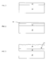
- FIG. 1 illustrates a method including forming a porous layer on a diamond support in accordance with certain embodiments
- FIG. 2 illustrates a method including forming a diamond seed layer on the porous layer of FIG. 1 , in accordance with certain embodiments
- FIG. 3 illustrates a method including forming a diamond layer in accordance with certain embodiments
- FIG. 4 illustrates a method including forming a layer on the diamond layer of FIG. 3 , in accordance with certain embodiments
- FIG. 5 illustrates a method including polishing the layer of FIG. 4 , in accordance with certain embodiments
- FIG. 6 illustrates a method including providing a semiconductor layer on the polished surface of FIG. 5 , in accordance with certain embodiments
- FIG. 7 illustrates a method including separating the diamond support and porous layer from the rest of the assembly, in accordance with certain embodiments
- FIG. 8 illustrated a method including providing a semiconductor layer on an adhesion layer on a surface of the diamond layer, in accordance with certain embodiments
- FIG. 9 is a flowchart illustrating operations in accordance with certain embodiments.
- FIG. 10 illustrates one embodiment of a computing environment in which aspects of the description provided herein are embodied.
- Certain embodiments relate to the formation of an assembly including a diamond substrate having a thin semiconductor layer thereon.
- Diamond is an advantageous material for thermal performance because it has a substantially higher thermal conductivity than copper or silicon.
- Diamond layers have been grown on silicon substrates. However, such diamond layers often have a high degree of warpage and thus are not suitable for the fabrication of devices such as transistors. Such warpage may be at least in part due to the thermal expansion mismatch between the silicon substrate and the diamond. The process for forming such a diamond layer requires relatively high temperatures and as such, the stresses developed due to the thermal expansion mismatch are substantial.
- FIGS. 1-3 illustrate a first embodiment of the present invention.
- a layer 12 is formed on a diamond support substrate 10 .
- the layer 12 is preferably a porous layer of material that can withstand relatively high processing temperatures used to form a diamond layer and that will enable such a diamond layer to be debonded from the diamond support substrate 10 .
- the layer 12 should preferably be formed from a non-organic material that can withstand the processing temperatures used in a CVD process for forming a diamond layer.
- An example of a preferred material for the layer 12 is SiO 2 .
- Another example of a material is silicon.
- the porosity may be in a preferred range of about 20 to 60 percent, with about 40 percent porosity being more preferred.
- the layer 12 is preferably formed to be considerably thinner than the diamond support substrate, with a preferred thickness in the range of about 1 ⁇ m to about 5 ⁇ m thick.
- the layer 12 also preferably has a coefficient of thermal expansion that is relatively close to that of diamond, to minimize stresses from thermal expansion mismatch.
- a substantially uniform seed layer 14 for the growth of polycrystalline diamond may be formed on the layer 12 , using a process such as those known in the art, so that the layer 12 is intermediate between the diamond support substrate 10 and the seed layer 14 .
- a diamond layer 16 is then formed on the seed layer 14 , for example, using a chemical vapor deposition (CVD) process as known in the art.
- CVD chemical vapor deposition
- One example of such a CVD process includes a hot filament microwave plasma process at about 800-1200° C.
- Other processes for forming a diamond layer as known in the art may also be used.
- the CVD diamond layer 16 is preferably formed to have a greater thickness than the layer 12 .
- the diamond layer 16 is preferably formed to have a thickness in the range of about 100 ⁇ m to about 500 ⁇ m thick, with one preferred embodiment being about 300 ⁇ m thick.
- a layer 18 is then formed on the diamond layer 16 .
- a preferred material for the layer 18 is polycrystalline silicon, formed to a preferred thickness in the range of up to about 20 ⁇ m, depending in part on the surface roughness of the CVD diamond layer 16 .
- Such a layer 18 is also preferably formed to have a grain size greater than 1 ⁇ m.
- the layer 18 may serve to facilitate the bonding of another layer to the diamond layer 16 and to facilitate forming a flat surface.
- the layer 18 is polished, to yield a flat surface 20 , as illustrated in FIGS. 4-5 . It is preferred that the polishing does not expose the diamond layer 16 .
- a die layer 22 is formed on the surface 20 of the layer 18 .
- the die layer 22 is preferably a thin die having a preferred thickness of up to about 3 ⁇ m, with a more preferred thickness of about 1 ⁇ m, although depending on various factors (such as the device to be formed, the materials used, etc.), other thicknesses may be used.
- the die layer 22 may be separately formed and then transferred to the surface 20 . Alternatively, the die layer 22 may be deposited or grown on the surface 20 .
- the die layer 22 may in certain embodiments be a single crystal silicon layer that has not yet been processed into an integrated circuit. Such a single crystal silicon layer may be bonded to the surface 20 using known methods.
- the diamond support substrate 10 is separated from the CVD diamond layer through the layer 12 , which, as noted earlier, in certain embodiments is preferably a porous SiO 2 layer.
- the separation may be carried out using a variety of techniques, including through the use of a liquid jet such as a water jet as known in the art to cut through the layer 12 .
- the remaining structure includes the CVD diamond layer 16 having the die layer 22 thereon.
- the separation of the diamond support layer 10 from the CVD diamond layer 16 may also be carried out using other techniques as known in the art, including, but not limited to, cleaving and mechanical shock.
- any remaining porous SiO 2 on the diamond layer 16 or on the diamond support substrate 10 thereon may be cleaned or polished off.
- additional processing may then be carried out on the die layer 22 .
- the diamond support substrate 10 may also be reused.
- a layer 12 is formed on a diamond support substrate 10 .
- the layer 12 may preferably be a porous SiO 2 layer.
- a diamond layer 16 (such as a CVD diamond layer) is then formed on the layer 12 .
- the diamond layer 16 may be formed by first depositing a seed layer 14 and then growing the diamond layer, using a known method as described above. The resultant structure appears in FIG. 3 , and includes the layer 12 positioned between the diamond support substrate 10 and the diamond layer 16 .
- the diamond support substrate from the diamond layer 16 by breaking through the layer 12 , which is preferably a porous layer of SiO 2 .
- the surface 15 of the diamond layer 16 may be of sufficient flatness so that it can be bonded to a die layer 22 without performing an additional polishing operation.
- a die layer 22 is positioned on the surface 15 of the diamond layer 16
- the diamond is positioned on the polished surface 20 on the other side of the diamond layer 16 .
- an optional adhesion layer 26 may be formed on the diamond layer surface 15 , if desired, to aid in the adhesion of the die layer 22 to the diamond layer 16 .
- Such an adhesion layer may be formed from a material such as a metal or a metal compound. Specific examples include, for example, titanium, titanium nitride, silicon oxide, and a variety of solders.
- the die layer 22 may be separately formed and then coupled to the diamond layer surface 15 . Alternatively, the die layer 22 may be deposited or grown on the surface 15 .
- the die layer 22 may in certain embodiments be a single crystal silicon layer that has not yet been processed into an integrated circuit. Such a single crystal silicon layer may be bonded to the surface 15 using known methods, and, as noted above, may be bonded to the surface 15 through an adhesion layer 26 .
- FIG. 9 illustrates embodiments in flow chart form including methods for forming an assembly including a semiconductor layer on a diamond support.
- Block 30 is forming a porous layer (such as SiO 2 ) on a preexisting diamond support.
- Block 32 is forming a CVD diamond layer (CVDD) on the porous layer so that the porous layer is positioned between the diamond support and the CVD diamond layer.
- Blocks 34 - 38 relate to an embodiment in which the diamond support is separated from the CVD diamond layer prior to providing a semiconductor layer on a surface of the CVD diamond layer.
- Blocks 40 - 46 relate to an embodiment in which the diamond support is separated from the CVD diamond layer after providing a semiconductor layer on a different surface of the CVD diamond layer.
- Block 34 is detaching the diamond support from the CVD diamond layer by breaking through the porous layer.
- Block 36 is forming an adhesion layer on the surface of the CV diamond layer that was in contact with the porous layer prior to removal of the porous layer.
- Block 38 is providing a semiconductor layer on the adhesion layer on the surface of the CVD diamond layer that was in contact with the porous layer.
- Block 40 is forming a polysilicon layer on the CVD diamond layer so that the CVD diamond layer is positioned between the porous layer and the polysilicon layer.
- Block 42 is polishing the polysilicon layer and forming a planarized surface including the polished polysilicon layer.
- Block 44 is providing a semiconductor layer on the planarized surface.
- Block 46 is detaching the diamond support by breaking through the porous layer.
- the embodiments described above yield a CVD diamond substrate layer having a semiconductor layer thereon.
- Such a structure can be formed to be thinner than conventional silicon-on-insulator structures.
- FIG. 10 illustrates one example of a computing environment in which aspects of described embodiments may be embodied.
- the computing environment includes a computer 70 including at least one central processing unit (CPU) 72 .
- the CPU 72 also referred to as a microprocessor, may be attached to an integrated circuit package 74 which is then coupled to a printed circuit board 78 , which in this embodiment, is a motherboard.
- the CPU 72 is an example of an assembly including a die layer 22 formed on a diamond substrate layer 16 as described earlier.
- the computer 70 further may further include memory 80 and one or more controllers 82 a , 82 b . . . 82 n which are also disposed on the motherboard 78 .
- the motherboard 78 may be a single layer or multi-layered board which has a plurality of conductive lines that provide communication between the circuits in the package 74 and other components mounted to the board 78 .
- one or more of the CPU 72 , memory 80 and controllers 82 a , 82 b . . . 82 n may be disposed on other cards such as daughter cards or expansion cards.
- the CPU 72 , memory 80 and controllers 82 a , 82 b . . . 82 n may each be seated in individual sockets or may be connected directly to a printed circuit board.
- a display 86 may also be included.
- the computer 70 may comprise any computing device known in the art, such as a mainframe, server, personal computer, workstation, laptop, handheld computer, telephony device, network appliance, virtualization device, storage controller, network controller, etc.
- the controllers 82 a , 82 b . . . 82 n may include a system controller, peripheral controller, memory controller, hub controller, I/O bus controller, video controller, network controller, storage controller, etc.
- a storage controller can control the reading of data from and the writing of data to the storage 84 in accordance with a storage protocol layer.
- the storage protocol of the layer may be any of a number of known storage protocols.
- Data being written to or read from the storage 84 may be cached in accordance with known caching techniques.
- a network controller can include one or more protocol layers to send and receive network packets to and from remote devices over a network 88 .
- the network 88 may comprise a Local Area Network (LAN), the Internet, a Wide Area Network (WAN), Storage Area Network (SAN), etc. Embodiments may be configured to transmit data over a wireless network or connection.
- the network controller and various protocol layers may employ the Ethernet protocol over unshielded twisted pair cable, token ring protocol, Fibre Channel protocol, etc., or any other network communication protocol known in the art.
Abstract
Description
Claims (20)
Priority Applications (1)
| Application Number | Priority Date | Filing Date | Title |
|---|---|---|---|
| US10/960,303 US7713839B2 (en) | 2004-10-06 | 2004-10-06 | Diamond substrate formation for electronic assemblies |
Applications Claiming Priority (1)
| Application Number | Priority Date | Filing Date | Title |
|---|---|---|---|
| US10/960,303 US7713839B2 (en) | 2004-10-06 | 2004-10-06 | Diamond substrate formation for electronic assemblies |
Publications (2)
| Publication Number | Publication Date |
|---|---|
| US20060073640A1 US20060073640A1 (en) | 2006-04-06 |
| US7713839B2 true US7713839B2 (en) | 2010-05-11 |
Family
ID=36126081
Family Applications (1)
| Application Number | Title | Priority Date | Filing Date |
|---|---|---|---|
| US10/960,303 Expired - Fee Related US7713839B2 (en) | 2004-10-06 | 2004-10-06 | Diamond substrate formation for electronic assemblies |
Country Status (1)
| Country | Link |
|---|---|
| US (1) | US7713839B2 (en) |
Cited By (3)
| Publication number | Priority date | Publication date | Assignee | Title |
|---|---|---|---|---|
| US20140205071A1 (en) * | 2013-01-18 | 2014-07-24 | Canon Kabushiki Kaisha | Transmission-type x-ray target and radiation generating tube including the same |
| US10584412B2 (en) | 2016-03-08 | 2020-03-10 | Ii-Vi Delaware, Inc. | Substrate comprising a layer of silicon and a layer of diamond having an optically finished (or a dense) silicon-diamond interface |
| US11146243B2 (en) * | 2017-06-19 | 2021-10-12 | Rfhic Corporation | Bulk acoustic wave filter |
Families Citing this family (5)
| Publication number | Priority date | Publication date | Assignee | Title |
|---|---|---|---|---|
| WO2007084501A2 (en) * | 2006-01-13 | 2007-07-26 | Group4 Labs, Llc | Method for manufacturing smooth diamond heat sinks |
| WO2008091910A2 (en) * | 2007-01-22 | 2008-07-31 | Group4 Labs, Llc | Composite wafers having bulk-quality semiconductor layers |
| WO2008148095A1 (en) * | 2007-05-25 | 2008-12-04 | Astralux, Inc. | Hybrid silicon/non-silicon electronic device with heat spreader |
| WO2011073716A1 (en) * | 2009-12-15 | 2011-06-23 | S.O.I. Tec Silicon On Insulator Technologies | Process for recycling a substrate. |
| JP6100036B2 (en) | 2013-03-12 | 2017-03-22 | キヤノン株式会社 | Transmission type target, radiation generating tube including the transmission type target, radiation generation apparatus, and radiation imaging apparatus |
Citations (32)
| Publication number | Priority date | Publication date | Assignee | Title |
|---|---|---|---|---|
| US4582954A (en) | 1983-10-26 | 1986-04-15 | Plessey Overseas Limited | Diamond heatsink assemblies |
| US5180571A (en) | 1990-05-30 | 1993-01-19 | Idemitsu Petrochemical Company Limited | Process for the preparation of diamond |
| US5350662A (en) | 1992-03-26 | 1994-09-27 | Hughes Aircraft Company | Maskless process for forming refractory metal layer in via holes of GaAs chips |
| US5906042A (en) | 1995-10-04 | 1999-05-25 | Prolinx Labs Corporation | Method and structure to interconnect traces of two conductive layers in a printed circuit board |
| US5962815A (en) | 1995-01-18 | 1999-10-05 | Prolinx Labs Corporation | Antifuse interconnect between two conducting layers of a printed circuit board |
| US6153938A (en) | 1997-07-28 | 2000-11-28 | Hitachi, Ltd. | Flip-chip connecting method, flip-chip connected structure and electronic device using the same |
| US20020056909A1 (en) | 1998-12-15 | 2002-05-16 | Heung-Kyu Kwon | Semiconductor chip package and method of fabricating the same |
| US20020074649A1 (en) | 2000-12-14 | 2002-06-20 | Intel Corporation | Electronic assembly with high capacity thermal interface and methods of manufacture |
| US20020141155A1 (en) | 1999-10-28 | 2002-10-03 | P1 Diamond, Inc., A California Corporation | Thermal management components |
| US6504723B1 (en) | 2001-11-15 | 2003-01-07 | Intel Corporation | Electronic assembly having solder thermal interface between a die substrate and a heat spreader |
| US6504242B1 (en) | 2001-11-15 | 2003-01-07 | Intel Corporation | Electronic assembly having a wetting layer on a thermally conductive heat spreader |
| US6549407B1 (en) | 2001-12-27 | 2003-04-15 | Intel Corporation | Heat exchanger retention mechanism |
| US20030117775A1 (en) | 2001-12-20 | 2003-06-26 | Vrtis Joan K. | Coated heat spreaders |
| US20030127715A1 (en) | 2002-01-07 | 2003-07-10 | Cheng-Yi Liu | Thinned die integrated circuit package |
| US20030132433A1 (en) * | 2002-01-15 | 2003-07-17 | Piner Edwin L. | Semiconductor structures including a gallium nitride material component and a silicon germanium component |
| US20030150604A1 (en) | 2002-02-08 | 2003-08-14 | Koning Paul A. | Polymer with solder pre-coated fillers for thermal interface materials |
| US20040029359A1 (en) * | 2000-11-27 | 2004-02-12 | Fabrice Letertre | Methods for fabricating a substrate |
| US20040052050A1 (en) | 2002-09-18 | 2004-03-18 | Koning Paul A. | Polymer solder hybrid |
| US6709898B1 (en) | 2000-10-04 | 2004-03-23 | Intel Corporation | Die-in-heat spreader microelectronic package |
| US20040066630A1 (en) | 2002-10-08 | 2004-04-08 | Whittenburg Kris J. | Integrated heat spreader package for heat transfer and for bond line thickness control and process of making |
| US6770966B2 (en) | 2001-07-31 | 2004-08-03 | Intel Corporation | Electronic assembly including a die having an integrated circuit and a layer of diamond to transfer heat |
| US20040233583A1 (en) * | 1999-06-03 | 2004-11-25 | Masahiro Yanagisawa | Magnetic disc apparatus and magnetic head in which a recording/reproduction element is mounted on a slider via a piezoelectric element |
| US6833289B2 (en) | 2003-05-12 | 2004-12-21 | Intel Corporation | Fluxless die-to-heat spreader bonding using thermal interface material |
| US20050161780A1 (en) | 2004-01-27 | 2005-07-28 | St Assembly Test Services Ltd. | Strip-fabricated flip chip in package and flip chip in system heat spreader assemblies and fabrication methods therefor |
| US6924170B2 (en) | 2003-06-30 | 2005-08-02 | Intel Corporation | Diamond-silicon hybrid integrated heat spreader |
| US6936497B2 (en) * | 2002-12-24 | 2005-08-30 | Intel Corporation | Method of forming electronic dies wherein each die has a layer of solid diamond |
| US20060046088A1 (en) * | 2004-09-02 | 2006-03-02 | Salman Akram | Selective nickel plating of aluminum, copper, and tungsten structures |
| US7033912B2 (en) * | 2004-01-22 | 2006-04-25 | Cree, Inc. | Silicon carbide on diamond substrates and related devices and methods |
| US7038277B2 (en) * | 2001-01-25 | 2006-05-02 | International Business Machines Corporation | Transferable device-containing layer for silicon-on-insulator applications |
| US7056810B2 (en) * | 2002-12-18 | 2006-06-06 | Semiconductor Energy Laboratory Co., Ltd. | Method for manufacturing semiconductor apparatus, and semiconductor apparatus and electric appliance |
| US7132309B2 (en) * | 2003-04-22 | 2006-11-07 | Chien-Min Sung | Semiconductor-on-diamond devices and methods of forming |
| US20070004216A1 (en) | 2005-06-30 | 2007-01-04 | Chuan Hu | Formation of assemblies with a diamond heat spreader |
Family Cites Families (1)
| Publication number | Priority date | Publication date | Assignee | Title |
|---|---|---|---|---|
| US3841413A (en) * | 1973-05-25 | 1974-10-15 | W Applewhite | Tractor attachment bar assembly with retractable portions |
-
2004
- 2004-10-06 US US10/960,303 patent/US7713839B2/en not_active Expired - Fee Related
Patent Citations (42)
| Publication number | Priority date | Publication date | Assignee | Title |
|---|---|---|---|---|
| US4582954A (en) | 1983-10-26 | 1986-04-15 | Plessey Overseas Limited | Diamond heatsink assemblies |
| US5180571A (en) | 1990-05-30 | 1993-01-19 | Idemitsu Petrochemical Company Limited | Process for the preparation of diamond |
| US5350662A (en) | 1992-03-26 | 1994-09-27 | Hughes Aircraft Company | Maskless process for forming refractory metal layer in via holes of GaAs chips |
| US5962815A (en) | 1995-01-18 | 1999-10-05 | Prolinx Labs Corporation | Antifuse interconnect between two conducting layers of a printed circuit board |
| US5906042A (en) | 1995-10-04 | 1999-05-25 | Prolinx Labs Corporation | Method and structure to interconnect traces of two conductive layers in a printed circuit board |
| US6153938A (en) | 1997-07-28 | 2000-11-28 | Hitachi, Ltd. | Flip-chip connecting method, flip-chip connected structure and electronic device using the same |
| US20020056909A1 (en) | 1998-12-15 | 2002-05-16 | Heung-Kyu Kwon | Semiconductor chip package and method of fabricating the same |
| US20040233583A1 (en) * | 1999-06-03 | 2004-11-25 | Masahiro Yanagisawa | Magnetic disc apparatus and magnetic head in which a recording/reproduction element is mounted on a slider via a piezoelectric element |
| US6919525B2 (en) | 1999-10-28 | 2005-07-19 | P1 Diamond, Inc. | Thermal management components |
| US20020141155A1 (en) | 1999-10-28 | 2002-10-03 | P1 Diamond, Inc., A California Corporation | Thermal management components |
| US6709898B1 (en) | 2000-10-04 | 2004-03-23 | Intel Corporation | Die-in-heat spreader microelectronic package |
| US20040029359A1 (en) * | 2000-11-27 | 2004-02-12 | Fabrice Letertre | Methods for fabricating a substrate |
| US20020105071A1 (en) | 2000-12-14 | 2002-08-08 | Mahajan Ravi V. | Electronic assembly with high capacity thermal spreader and methods of manufacture |
| US20020074649A1 (en) | 2000-12-14 | 2002-06-20 | Intel Corporation | Electronic assembly with high capacity thermal interface and methods of manufacture |
| US6706562B2 (en) | 2000-12-14 | 2004-03-16 | Intel Corporation | Electronic assembly with high capacity thermal spreader and methods of manufacture |
| US6653730B2 (en) | 2000-12-14 | 2003-11-25 | Intel Corporation | Electronic assembly with high capacity thermal interface |
| US7038277B2 (en) * | 2001-01-25 | 2006-05-02 | International Business Machines Corporation | Transferable device-containing layer for silicon-on-insulator applications |
| US6770966B2 (en) | 2001-07-31 | 2004-08-03 | Intel Corporation | Electronic assembly including a die having an integrated circuit and a layer of diamond to transfer heat |
| US6504723B1 (en) | 2001-11-15 | 2003-01-07 | Intel Corporation | Electronic assembly having solder thermal interface between a die substrate and a heat spreader |
| US6504242B1 (en) | 2001-11-15 | 2003-01-07 | Intel Corporation | Electronic assembly having a wetting layer on a thermally conductive heat spreader |
| US6751099B2 (en) | 2001-12-20 | 2004-06-15 | Intel Corporation | Coated heat spreaders |
| US20030117775A1 (en) | 2001-12-20 | 2003-06-26 | Vrtis Joan K. | Coated heat spreaders |
| US6549407B1 (en) | 2001-12-27 | 2003-04-15 | Intel Corporation | Heat exchanger retention mechanism |
| US20030127715A1 (en) | 2002-01-07 | 2003-07-10 | Cheng-Yi Liu | Thinned die integrated circuit package |
| US6841413B2 (en) | 2002-01-07 | 2005-01-11 | Intel Corporation | Thinned die integrated circuit package |
| US20030132433A1 (en) * | 2002-01-15 | 2003-07-17 | Piner Edwin L. | Semiconductor structures including a gallium nitride material component and a silicon germanium component |
| US7036573B2 (en) | 2002-02-08 | 2006-05-02 | Intel Corporation | Polymer with solder pre-coated fillers for thermal interface materials |
| US20030150604A1 (en) | 2002-02-08 | 2003-08-14 | Koning Paul A. | Polymer with solder pre-coated fillers for thermal interface materials |
| US20040052050A1 (en) | 2002-09-18 | 2004-03-18 | Koning Paul A. | Polymer solder hybrid |
| US6813153B2 (en) | 2002-09-18 | 2004-11-02 | Intel Corporation | Polymer solder hybrid |
| US6867978B2 (en) | 2002-10-08 | 2005-03-15 | Intel Corporation | Integrated heat spreader package for heat transfer and for bond line thickness control and process of making |
| US20040066630A1 (en) | 2002-10-08 | 2004-04-08 | Whittenburg Kris J. | Integrated heat spreader package for heat transfer and for bond line thickness control and process of making |
| US7056810B2 (en) * | 2002-12-18 | 2006-06-06 | Semiconductor Energy Laboratory Co., Ltd. | Method for manufacturing semiconductor apparatus, and semiconductor apparatus and electric appliance |
| US6936497B2 (en) * | 2002-12-24 | 2005-08-30 | Intel Corporation | Method of forming electronic dies wherein each die has a layer of solid diamond |
| US7132309B2 (en) * | 2003-04-22 | 2006-11-07 | Chien-Min Sung | Semiconductor-on-diamond devices and methods of forming |
| US6833289B2 (en) | 2003-05-12 | 2004-12-21 | Intel Corporation | Fluxless die-to-heat spreader bonding using thermal interface material |
| US6924170B2 (en) | 2003-06-30 | 2005-08-02 | Intel Corporation | Diamond-silicon hybrid integrated heat spreader |
| US7033912B2 (en) * | 2004-01-22 | 2006-04-25 | Cree, Inc. | Silicon carbide on diamond substrates and related devices and methods |
| US20050161780A1 (en) | 2004-01-27 | 2005-07-28 | St Assembly Test Services Ltd. | Strip-fabricated flip chip in package and flip chip in system heat spreader assemblies and fabrication methods therefor |
| US7153725B2 (en) | 2004-01-27 | 2006-12-26 | St Assembly Test Services Ltd. | Strip-fabricated flip chip in package and flip chip in system heat spreader assemblies and fabrication methods therefor |
| US20060046088A1 (en) * | 2004-09-02 | 2006-03-02 | Salman Akram | Selective nickel plating of aluminum, copper, and tungsten structures |
| US20070004216A1 (en) | 2005-06-30 | 2007-01-04 | Chuan Hu | Formation of assemblies with a diamond heat spreader |
Non-Patent Citations (1)
| Title |
|---|
| U.S. Appl. No. 11/173,834, Hu et al., entitled "Formation Of Assemblies With A Diamond Heat Spreader", published as US 20070004216 A1 (filed Jun. 30, 2005, publication date Jan. 4, 2007). |
Cited By (6)
| Publication number | Priority date | Publication date | Assignee | Title |
|---|---|---|---|---|
| US20140205071A1 (en) * | 2013-01-18 | 2014-07-24 | Canon Kabushiki Kaisha | Transmission-type x-ray target and radiation generating tube including the same |
| US9502204B2 (en) * | 2013-01-18 | 2016-11-22 | Canon Kabushiki Kaisha | Transmission-type X-ray target and radiation generating tube including the same |
| US10584412B2 (en) | 2016-03-08 | 2020-03-10 | Ii-Vi Delaware, Inc. | Substrate comprising a layer of silicon and a layer of diamond having an optically finished (or a dense) silicon-diamond interface |
| US11313037B2 (en) | 2016-03-08 | 2022-04-26 | Ii-Vi Delaware, Inc. | Method of forming a multilayer substrate comprising a layer of silicon and a layer of diamond having an optically finished (or a dense) silicon-diamond interface |
| US11891691B2 (en) | 2016-03-08 | 2024-02-06 | Ii-Vi Delaware, Inc. | Method of forming a multilayer substrate comprising a layer of silicon and a layer of diamond having an optically finished (or a dense) silicon-diamond interface |
| US11146243B2 (en) * | 2017-06-19 | 2021-10-12 | Rfhic Corporation | Bulk acoustic wave filter |
Also Published As
| Publication number | Publication date |
|---|---|
| US20060073640A1 (en) | 2006-04-06 |
Similar Documents
| Publication | Publication Date | Title |
|---|---|---|
| CN1327505C (en) | Method for making stacked structure comprising thin film adhering to target substrate | |
| Crnogorac et al. | Semiconductor crystal islands for three-dimensional integration | |
| KR101876912B1 (en) | Electronic device for radiofrequency or power applications and process for manufacturing such a device | |
| US7550841B2 (en) | Methods of forming a diamond micro-channel structure and resulting devices | |
| US7749863B1 (en) | Thermal management substrates | |
| US20050017351A1 (en) | Silicon on diamond wafers and devices | |
| CN104054171A (en) | Flattened substrate surface for substrate bonding | |
| US7713839B2 (en) | Diamond substrate formation for electronic assemblies | |
| JPH11145438A (en) | Method of manufacturing soi wafer and soi wafer manufactured by the method | |
| US20080119046A1 (en) | Method of making a contact on a backside of a die | |
| US7875934B2 (en) | Semiconductor substrate with islands of diamond and resulting devices | |
| US11361969B2 (en) | Device substrate with high thermal conductivity and method of manufacturing the same | |
| US7285479B2 (en) | Semiconductor device and method for manufacturing multilayered substrate for semiconductor device | |
| TWI233179B (en) | Manufacturing method of mounting body, semiconductor device and mounting body | |
| US20040191534A1 (en) | Stress-reducing structure for electronic devices | |
| JP2008526009A (en) | How to move a circuit to a ground plane | |
| US7531429B2 (en) | Methods and apparatuses for manufacturing ultra thin device layers for integrated circuit devices | |
| EP3109893B1 (en) | Composite substrate | |
| JP2002525839A (en) | Thin-film semiconductor structure having a heat conducting layer | |
| US20070004216A1 (en) | Formation of assemblies with a diamond heat spreader | |
| CN109830484B (en) | SOI structure and manufacturing process thereof | |
| US7466019B2 (en) | Rectangular semi-conducting support for microelectronics and method for making same | |
| US20140319612A1 (en) | Semiconductor-on-insulator structure and process for producing same | |
| JPH0992802A (en) | Soi substrate and its manufacture | |
| JPS62159444A (en) | Manufacture of semiconductor device |
Legal Events
| Date | Code | Title | Description |
|---|---|---|---|
| AS | Assignment |
Owner name: INTEL CORPORATION, CALIFORNIA Free format text: ASSIGNMENT OF ASSIGNORS INTEREST;ASSIGNORS:HU, CHUAN;CHRYSLER, GREGORY M.;LU, DAOQIANG;REEL/FRAME:015884/0929 Effective date: 20041005 Owner name: INTEL CORPORATION,CALIFORNIA Free format text: ASSIGNMENT OF ASSIGNORS INTEREST;ASSIGNORS:HU, CHUAN;CHRYSLER, GREGORY M.;LU, DAOQIANG;REEL/FRAME:015884/0929 Effective date: 20041005 |
|
| FPAY | Fee payment |
Year of fee payment: 4 |
|
| CC | Certificate of correction | ||
| FEPP | Fee payment procedure |
Free format text: MAINTENANCE FEE REMINDER MAILED (ORIGINAL EVENT CODE: REM.) |
|
| LAPS | Lapse for failure to pay maintenance fees |
Free format text: PATENT EXPIRED FOR FAILURE TO PAY MAINTENANCE FEES (ORIGINAL EVENT CODE: EXP.) |
|
| STCH | Information on status: patent discontinuation |
Free format text: PATENT EXPIRED DUE TO NONPAYMENT OF MAINTENANCE FEES UNDER 37 CFR 1.362 |