US7730606B2 - Manufacturing method for a wireless communication device and manufacturing apparatus - Google Patents
Manufacturing method for a wireless communication device and manufacturing apparatus Download PDFInfo
- Publication number
- US7730606B2 US7730606B2 US11/468,749 US46874906A US7730606B2 US 7730606 B2 US7730606 B2 US 7730606B2 US 46874906 A US46874906 A US 46874906A US 7730606 B2 US7730606 B2 US 7730606B2
- Authority
- US
- United States
- Prior art keywords
- wireless communication
- tab
- communication chip
- substrate
- cutting
- Prior art date
- Legal status (The legal status is an assumption and is not a legal conclusion. Google has not performed a legal analysis and makes no representation as to the accuracy of the status listed.)
- Expired - Fee Related, expires
Links
- 238000004891 communication Methods 0.000 title claims abstract description 94
- 238000004519 manufacturing process Methods 0.000 title claims abstract description 33
- 239000000758 substrate Substances 0.000 claims abstract description 59
- 238000005520 cutting process Methods 0.000 claims abstract description 48
- 239000000853 adhesive Substances 0.000 claims description 37
- 230000001070 adhesive effect Effects 0.000 claims description 37
- 239000011888 foil Substances 0.000 claims description 16
- 239000000463 material Substances 0.000 claims description 15
- 238000007789 sealing Methods 0.000 claims description 11
- 229910000679 solder Inorganic materials 0.000 claims description 11
- 239000004033 plastic Substances 0.000 claims description 5
- 229920003023 plastic Polymers 0.000 claims description 5
- 239000000155 melt Substances 0.000 claims description 3
- 230000005855 radiation Effects 0.000 claims description 3
- 239000004593 Epoxy Substances 0.000 claims description 2
- 238000003780 insertion Methods 0.000 claims description 2
- 230000037431 insertion Effects 0.000 claims description 2
- 238000001816 cooling Methods 0.000 claims 1
- 230000008878 coupling Effects 0.000 claims 1
- 238000010168 coupling process Methods 0.000 claims 1
- 238000005859 coupling reaction Methods 0.000 claims 1
- 238000000034 method Methods 0.000 abstract description 58
- 239000004020 conductor Substances 0.000 description 7
- 238000012545 processing Methods 0.000 description 5
- 238000012360 testing method Methods 0.000 description 5
- 239000002699 waste material Substances 0.000 description 5
- 229910052782 aluminium Inorganic materials 0.000 description 4
- XAGFODPZIPBFFR-UHFFFAOYSA-N aluminium Chemical compound [Al] XAGFODPZIPBFFR-UHFFFAOYSA-N 0.000 description 4
- 238000002844 melting Methods 0.000 description 4
- 230000008018 melting Effects 0.000 description 4
- RYGMFSIKBFXOCR-UHFFFAOYSA-N Copper Chemical compound [Cu] RYGMFSIKBFXOCR-UHFFFAOYSA-N 0.000 description 3
- 238000003466 welding Methods 0.000 description 3
- XEEYBQQBJWHFJM-UHFFFAOYSA-N Iron Chemical compound [Fe] XEEYBQQBJWHFJM-UHFFFAOYSA-N 0.000 description 2
- 239000012876 carrier material Substances 0.000 description 2
- 229910052802 copper Inorganic materials 0.000 description 2
- 239000010949 copper Substances 0.000 description 2
- 229910052751 metal Inorganic materials 0.000 description 2
- 239000002184 metal Substances 0.000 description 2
- 238000012546 transfer Methods 0.000 description 2
- 229920002799 BoPET Polymers 0.000 description 1
- CWYNVVGOOAEACU-UHFFFAOYSA-N Fe2+ Chemical compound [Fe+2] CWYNVVGOOAEACU-UHFFFAOYSA-N 0.000 description 1
- 239000005041 Mylar™ Substances 0.000 description 1
- 239000004642 Polyimide Substances 0.000 description 1
- 239000004743 Polypropylene Substances 0.000 description 1
- 229910000831 Steel Inorganic materials 0.000 description 1
- 239000011889 copper foil Substances 0.000 description 1
- 230000003247 decreasing effect Effects 0.000 description 1
- 230000002950 deficient Effects 0.000 description 1
- 238000013461 design Methods 0.000 description 1
- 238000010586 diagram Methods 0.000 description 1
- 230000007613 environmental effect Effects 0.000 description 1
- 238000010348 incorporation Methods 0.000 description 1
- 230000010354 integration Effects 0.000 description 1
- 229910052742 iron Inorganic materials 0.000 description 1
- 230000005404 monopole Effects 0.000 description 1
- 229920001721 polyimide Polymers 0.000 description 1
- -1 polypropylene Polymers 0.000 description 1
- 229920001155 polypropylene Polymers 0.000 description 1
- 229920001296 polysiloxane Polymers 0.000 description 1
- 238000004080 punching Methods 0.000 description 1
- 230000004044 response Effects 0.000 description 1
- 239000010959 steel Substances 0.000 description 1
Images


Classifications
-
- G—PHYSICS
- G06—COMPUTING; CALCULATING OR COUNTING
- G06K—GRAPHICAL DATA READING; PRESENTATION OF DATA; RECORD CARRIERS; HANDLING RECORD CARRIERS
- G06K19/00—Record carriers for use with machines and with at least a part designed to carry digital markings
- G06K19/06—Record carriers for use with machines and with at least a part designed to carry digital markings characterised by the kind of the digital marking, e.g. shape, nature, code
- G06K19/067—Record carriers with conductive marks, printed circuits or semiconductor circuit elements, e.g. credit or identity cards also with resonating or responding marks without active components
- G06K19/07—Record carriers with conductive marks, printed circuits or semiconductor circuit elements, e.g. credit or identity cards also with resonating or responding marks without active components with integrated circuit chips
- G06K19/077—Constructional details, e.g. mounting of circuits in the carrier
- G06K19/07745—Mounting details of integrated circuit chips
-
- G—PHYSICS
- G06—COMPUTING; CALCULATING OR COUNTING
- G06K—GRAPHICAL DATA READING; PRESENTATION OF DATA; RECORD CARRIERS; HANDLING RECORD CARRIERS
- G06K19/00—Record carriers for use with machines and with at least a part designed to carry digital markings
- G06K19/06—Record carriers for use with machines and with at least a part designed to carry digital markings characterised by the kind of the digital marking, e.g. shape, nature, code
- G06K19/067—Record carriers with conductive marks, printed circuits or semiconductor circuit elements, e.g. credit or identity cards also with resonating or responding marks without active components
- G06K19/07—Record carriers with conductive marks, printed circuits or semiconductor circuit elements, e.g. credit or identity cards also with resonating or responding marks without active components with integrated circuit chips
- G06K19/077—Constructional details, e.g. mounting of circuits in the carrier
- G06K19/07718—Constructional details, e.g. mounting of circuits in the carrier the record carrier being manufactured in a continuous process, e.g. using endless rolls
-
- G—PHYSICS
- G06—COMPUTING; CALCULATING OR COUNTING
- G06K—GRAPHICAL DATA READING; PRESENTATION OF DATA; RECORD CARRIERS; HANDLING RECORD CARRIERS
- G06K19/00—Record carriers for use with machines and with at least a part designed to carry digital markings
- G06K19/06—Record carriers for use with machines and with at least a part designed to carry digital markings characterised by the kind of the digital marking, e.g. shape, nature, code
- G06K19/067—Record carriers with conductive marks, printed circuits or semiconductor circuit elements, e.g. credit or identity cards also with resonating or responding marks without active components
- G06K19/07—Record carriers with conductive marks, printed circuits or semiconductor circuit elements, e.g. credit or identity cards also with resonating or responding marks without active components with integrated circuit chips
- G06K19/077—Constructional details, e.g. mounting of circuits in the carrier
- G06K19/07749—Constructional details, e.g. mounting of circuits in the carrier the record carrier being capable of non-contact communication, e.g. constructional details of the antenna of a non-contact smart card
- G06K19/07773—Antenna details
- G06K19/07786—Antenna details the antenna being of the HF type, such as a dipole
-
- H—ELECTRICITY
- H01—ELECTRIC ELEMENTS
- H01L—SEMICONDUCTOR DEVICES NOT COVERED BY CLASS H10
- H01L23/00—Details of semiconductor or other solid state devices
- H01L23/48—Arrangements for conducting electric current to or from the solid state body in operation, e.g. leads, terminal arrangements ; Selection of materials therefor
- H01L23/488—Arrangements for conducting electric current to or from the solid state body in operation, e.g. leads, terminal arrangements ; Selection of materials therefor consisting of soldered or bonded constructions
- H01L23/498—Leads, i.e. metallisations or lead-frames on insulating substrates, e.g. chip carriers
- H01L23/49855—Leads, i.e. metallisations or lead-frames on insulating substrates, e.g. chip carriers for flat-cards, e.g. credit cards
-
- H—ELECTRICITY
- H01—ELECTRIC ELEMENTS
- H01Q—ANTENNAS, i.e. RADIO AERIALS
- H01Q9/00—Electrically-short antennas having dimensions not more than twice the operating wavelength and consisting of conductive active radiating elements
- H01Q9/04—Resonant antennas
- H01Q9/16—Resonant antennas with feed intermediate between the extremities of the antenna, e.g. centre-fed dipole
- H01Q9/28—Conical, cylindrical, cage, strip, gauze, or like elements having an extended radiating surface; Elements comprising two conical surfaces having collinear axes and adjacent apices and fed by two-conductor transmission lines
- H01Q9/285—Planar dipole
-
- H—ELECTRICITY
- H01—ELECTRIC ELEMENTS
- H01L—SEMICONDUCTOR DEVICES NOT COVERED BY CLASS H10
- H01L2924/00—Indexing scheme for arrangements or methods for connecting or disconnecting semiconductor or solid-state bodies as covered by H01L24/00
- H01L2924/0001—Technical content checked by a classifier
- H01L2924/0002—Not covered by any one of groups H01L24/00, H01L24/00 and H01L2224/00
-
- H—ELECTRICITY
- H01—ELECTRIC ELEMENTS
- H01L—SEMICONDUCTOR DEVICES NOT COVERED BY CLASS H10
- H01L2924/00—Indexing scheme for arrangements or methods for connecting or disconnecting semiconductor or solid-state bodies as covered by H01L24/00
- H01L2924/30—Technical effects
- H01L2924/301—Electrical effects
- H01L2924/3011—Impedance
-
- H—ELECTRICITY
- H05—ELECTRIC TECHNIQUES NOT OTHERWISE PROVIDED FOR
- H05K—PRINTED CIRCUITS; CASINGS OR CONSTRUCTIONAL DETAILS OF ELECTRIC APPARATUS; MANUFACTURE OF ASSEMBLAGES OF ELECTRICAL COMPONENTS
- H05K1/00—Printed circuits
- H05K1/18—Printed circuits structurally associated with non-printed electric components
- H05K1/182—Printed circuits structurally associated with non-printed electric components associated with components mounted in the printed circuit board, e.g. insert mounted components [IMC]
-
- H—ELECTRICITY
- H05—ELECTRIC TECHNIQUES NOT OTHERWISE PROVIDED FOR
- H05K—PRINTED CIRCUITS; CASINGS OR CONSTRUCTIONAL DETAILS OF ELECTRIC APPARATUS; MANUFACTURE OF ASSEMBLAGES OF ELECTRICAL COMPONENTS
- H05K3/00—Apparatus or processes for manufacturing printed circuits
- H05K3/02—Apparatus or processes for manufacturing printed circuits in which the conductive material is applied to the surface of the insulating support and is thereafter removed from such areas of the surface which are not intended for current conducting or shielding
- H05K3/04—Apparatus or processes for manufacturing printed circuits in which the conductive material is applied to the surface of the insulating support and is thereafter removed from such areas of the surface which are not intended for current conducting or shielding the conductive material being removed mechanically, e.g. by punching
- H05K3/041—Apparatus or processes for manufacturing printed circuits in which the conductive material is applied to the surface of the insulating support and is thereafter removed from such areas of the surface which are not intended for current conducting or shielding the conductive material being removed mechanically, e.g. by punching by using a die for cutting the conductive material
-
- H—ELECTRICITY
- H05—ELECTRIC TECHNIQUES NOT OTHERWISE PROVIDED FOR
- H05K—PRINTED CIRCUITS; CASINGS OR CONSTRUCTIONAL DETAILS OF ELECTRIC APPARATUS; MANUFACTURE OF ASSEMBLAGES OF ELECTRICAL COMPONENTS
- H05K3/00—Apparatus or processes for manufacturing printed circuits
- H05K3/30—Assembling printed circuits with electric components, e.g. with resistor
- H05K3/32—Assembling printed circuits with electric components, e.g. with resistor electrically connecting electric components or wires to printed circuits
- H05K3/325—Assembling printed circuits with electric components, e.g. with resistor electrically connecting electric components or wires to printed circuits by abutting or pinching, i.e. without alloying process; mechanical auxiliary parts therefor
- H05K3/326—Assembling printed circuits with electric components, e.g. with resistor electrically connecting electric components or wires to printed circuits by abutting or pinching, i.e. without alloying process; mechanical auxiliary parts therefor the printed circuit having integral resilient or deformable parts, e.g. tabs or parts of flexible circuits
-
- Y—GENERAL TAGGING OF NEW TECHNOLOGICAL DEVELOPMENTS; GENERAL TAGGING OF CROSS-SECTIONAL TECHNOLOGIES SPANNING OVER SEVERAL SECTIONS OF THE IPC; TECHNICAL SUBJECTS COVERED BY FORMER USPC CROSS-REFERENCE ART COLLECTIONS [XRACs] AND DIGESTS
- Y10—TECHNICAL SUBJECTS COVERED BY FORMER USPC
- Y10T—TECHNICAL SUBJECTS COVERED BY FORMER US CLASSIFICATION
- Y10T156/00—Adhesive bonding and miscellaneous chemical manufacture
- Y10T156/10—Methods of surface bonding and/or assembly therefor
- Y10T156/1052—Methods of surface bonding and/or assembly therefor with cutting, punching, tearing or severing
- Y10T156/1062—Prior to assembly
- Y10T156/1075—Prior to assembly of plural laminae from single stock and assembling to each other or to additional lamina
-
- Y—GENERAL TAGGING OF NEW TECHNOLOGICAL DEVELOPMENTS; GENERAL TAGGING OF CROSS-SECTIONAL TECHNOLOGIES SPANNING OVER SEVERAL SECTIONS OF THE IPC; TECHNICAL SUBJECTS COVERED BY FORMER USPC CROSS-REFERENCE ART COLLECTIONS [XRACs] AND DIGESTS
- Y10—TECHNICAL SUBJECTS COVERED BY FORMER USPC
- Y10T—TECHNICAL SUBJECTS COVERED BY FORMER US CLASSIFICATION
- Y10T156/00—Adhesive bonding and miscellaneous chemical manufacture
- Y10T156/10—Methods of surface bonding and/or assembly therefor
- Y10T156/1089—Methods of surface bonding and/or assembly therefor of discrete laminae to single face of additional lamina
- Y10T156/1092—All laminae planar and face to face
- Y10T156/1097—Lamina is running length web
-
- Y—GENERAL TAGGING OF NEW TECHNOLOGICAL DEVELOPMENTS; GENERAL TAGGING OF CROSS-SECTIONAL TECHNOLOGIES SPANNING OVER SEVERAL SECTIONS OF THE IPC; TECHNICAL SUBJECTS COVERED BY FORMER USPC CROSS-REFERENCE ART COLLECTIONS [XRACs] AND DIGESTS
- Y10—TECHNICAL SUBJECTS COVERED BY FORMER USPC
- Y10T—TECHNICAL SUBJECTS COVERED BY FORMER US CLASSIFICATION
- Y10T29/00—Metal working
- Y10T29/49—Method of mechanical manufacture
- Y10T29/49002—Electrical device making
- Y10T29/49004—Electrical device making including measuring or testing of device or component part
-
- Y—GENERAL TAGGING OF NEW TECHNOLOGICAL DEVELOPMENTS; GENERAL TAGGING OF CROSS-SECTIONAL TECHNOLOGIES SPANNING OVER SEVERAL SECTIONS OF THE IPC; TECHNICAL SUBJECTS COVERED BY FORMER USPC CROSS-REFERENCE ART COLLECTIONS [XRACs] AND DIGESTS
- Y10—TECHNICAL SUBJECTS COVERED BY FORMER USPC
- Y10T—TECHNICAL SUBJECTS COVERED BY FORMER US CLASSIFICATION
- Y10T29/00—Metal working
- Y10T29/49—Method of mechanical manufacture
- Y10T29/49002—Electrical device making
- Y10T29/49016—Antenna or wave energy "plumbing" making
- Y10T29/49018—Antenna or wave energy "plumbing" making with other electrical component
-
- Y—GENERAL TAGGING OF NEW TECHNOLOGICAL DEVELOPMENTS; GENERAL TAGGING OF CROSS-SECTIONAL TECHNOLOGIES SPANNING OVER SEVERAL SECTIONS OF THE IPC; TECHNICAL SUBJECTS COVERED BY FORMER USPC CROSS-REFERENCE ART COLLECTIONS [XRACs] AND DIGESTS
- Y10—TECHNICAL SUBJECTS COVERED BY FORMER USPC
- Y10T—TECHNICAL SUBJECTS COVERED BY FORMER US CLASSIFICATION
- Y10T29/00—Metal working
- Y10T29/49—Method of mechanical manufacture
- Y10T29/49002—Electrical device making
- Y10T29/49117—Conductor or circuit manufacturing
- Y10T29/49121—Beam lead frame or beam lead device
-
- Y—GENERAL TAGGING OF NEW TECHNOLOGICAL DEVELOPMENTS; GENERAL TAGGING OF CROSS-SECTIONAL TECHNOLOGIES SPANNING OVER SEVERAL SECTIONS OF THE IPC; TECHNICAL SUBJECTS COVERED BY FORMER USPC CROSS-REFERENCE ART COLLECTIONS [XRACs] AND DIGESTS
- Y10—TECHNICAL SUBJECTS COVERED BY FORMER USPC
- Y10T—TECHNICAL SUBJECTS COVERED BY FORMER US CLASSIFICATION
- Y10T29/00—Metal working
- Y10T29/49—Method of mechanical manufacture
- Y10T29/49002—Electrical device making
- Y10T29/49117—Conductor or circuit manufacturing
- Y10T29/49124—On flat or curved insulated base, e.g., printed circuit, etc.
- Y10T29/49126—Assembling bases
-
- Y—GENERAL TAGGING OF NEW TECHNOLOGICAL DEVELOPMENTS; GENERAL TAGGING OF CROSS-SECTIONAL TECHNOLOGIES SPANNING OVER SEVERAL SECTIONS OF THE IPC; TECHNICAL SUBJECTS COVERED BY FORMER USPC CROSS-REFERENCE ART COLLECTIONS [XRACs] AND DIGESTS
- Y10—TECHNICAL SUBJECTS COVERED BY FORMER USPC
- Y10T—TECHNICAL SUBJECTS COVERED BY FORMER US CLASSIFICATION
- Y10T29/00—Metal working
- Y10T29/49—Method of mechanical manufacture
- Y10T29/49002—Electrical device making
- Y10T29/49117—Conductor or circuit manufacturing
- Y10T29/49124—On flat or curved insulated base, e.g., printed circuit, etc.
- Y10T29/49128—Assembling formed circuit to base
-
- Y—GENERAL TAGGING OF NEW TECHNOLOGICAL DEVELOPMENTS; GENERAL TAGGING OF CROSS-SECTIONAL TECHNOLOGIES SPANNING OVER SEVERAL SECTIONS OF THE IPC; TECHNICAL SUBJECTS COVERED BY FORMER USPC CROSS-REFERENCE ART COLLECTIONS [XRACs] AND DIGESTS
- Y10—TECHNICAL SUBJECTS COVERED BY FORMER USPC
- Y10T—TECHNICAL SUBJECTS COVERED BY FORMER US CLASSIFICATION
- Y10T29/00—Metal working
- Y10T29/49—Method of mechanical manufacture
- Y10T29/49002—Electrical device making
- Y10T29/49117—Conductor or circuit manufacturing
- Y10T29/49124—On flat or curved insulated base, e.g., printed circuit, etc.
- Y10T29/4913—Assembling to base an electrical component, e.g., capacitor, etc.
- Y10T29/49144—Assembling to base an electrical component, e.g., capacitor, etc. by metal fusion
-
- Y—GENERAL TAGGING OF NEW TECHNOLOGICAL DEVELOPMENTS; GENERAL TAGGING OF CROSS-SECTIONAL TECHNOLOGIES SPANNING OVER SEVERAL SECTIONS OF THE IPC; TECHNICAL SUBJECTS COVERED BY FORMER USPC CROSS-REFERENCE ART COLLECTIONS [XRACs] AND DIGESTS
- Y10—TECHNICAL SUBJECTS COVERED BY FORMER USPC
- Y10T—TECHNICAL SUBJECTS COVERED BY FORMER US CLASSIFICATION
- Y10T29/00—Metal working
- Y10T29/49—Method of mechanical manufacture
- Y10T29/49002—Electrical device making
- Y10T29/49117—Conductor or circuit manufacturing
- Y10T29/49124—On flat or curved insulated base, e.g., printed circuit, etc.
- Y10T29/49155—Manufacturing circuit on or in base
-
- Y—GENERAL TAGGING OF NEW TECHNOLOGICAL DEVELOPMENTS; GENERAL TAGGING OF CROSS-SECTIONAL TECHNOLOGIES SPANNING OVER SEVERAL SECTIONS OF THE IPC; TECHNICAL SUBJECTS COVERED BY FORMER USPC CROSS-REFERENCE ART COLLECTIONS [XRACs] AND DIGESTS
- Y10—TECHNICAL SUBJECTS COVERED BY FORMER USPC
- Y10T—TECHNICAL SUBJECTS COVERED BY FORMER US CLASSIFICATION
- Y10T29/00—Metal working
- Y10T29/49—Method of mechanical manufacture
- Y10T29/49751—Scrap recovering or utilizing
- Y10T29/49755—Separating one material from another
-
- Y—GENERAL TAGGING OF NEW TECHNOLOGICAL DEVELOPMENTS; GENERAL TAGGING OF CROSS-SECTIONAL TECHNOLOGIES SPANNING OVER SEVERAL SECTIONS OF THE IPC; TECHNICAL SUBJECTS COVERED BY FORMER USPC CROSS-REFERENCE ART COLLECTIONS [XRACs] AND DIGESTS
- Y10—TECHNICAL SUBJECTS COVERED BY FORMER USPC
- Y10T—TECHNICAL SUBJECTS COVERED BY FORMER US CLASSIFICATION
- Y10T29/00—Metal working
- Y10T29/51—Plural diverse manufacturing apparatus including means for metal shaping or assembling
- Y10T29/5136—Separate tool stations for selective or successive operation on work
- Y10T29/5137—Separate tool stations for selective or successive operation on work including assembling or disassembling station
- Y10T29/5139—Separate tool stations for selective or successive operation on work including assembling or disassembling station and means to sever work prior to disassembling
- Y10T29/514—Separate tool stations for selective or successive operation on work including assembling or disassembling station and means to sever work prior to disassembling comprising means to strip insulation from wire
-
- Y—GENERAL TAGGING OF NEW TECHNOLOGICAL DEVELOPMENTS; GENERAL TAGGING OF CROSS-SECTIONAL TECHNOLOGIES SPANNING OVER SEVERAL SECTIONS OF THE IPC; TECHNICAL SUBJECTS COVERED BY FORMER USPC CROSS-REFERENCE ART COLLECTIONS [XRACs] AND DIGESTS
- Y10—TECHNICAL SUBJECTS COVERED BY FORMER USPC
- Y10T—TECHNICAL SUBJECTS COVERED BY FORMER US CLASSIFICATION
- Y10T29/00—Metal working
- Y10T29/53—Means to assemble or disassemble
- Y10T29/5313—Means to assemble electrical device
- Y10T29/53165—Magnetic memory device
-
- Y—GENERAL TAGGING OF NEW TECHNOLOGICAL DEVELOPMENTS; GENERAL TAGGING OF CROSS-SECTIONAL TECHNOLOGIES SPANNING OVER SEVERAL SECTIONS OF THE IPC; TECHNICAL SUBJECTS COVERED BY FORMER USPC CROSS-REFERENCE ART COLLECTIONS [XRACs] AND DIGESTS
- Y10—TECHNICAL SUBJECTS COVERED BY FORMER USPC
- Y10T—TECHNICAL SUBJECTS COVERED BY FORMER US CLASSIFICATION
- Y10T29/00—Metal working
- Y10T29/53—Means to assemble or disassemble
- Y10T29/5313—Means to assemble electrical device
- Y10T29/5317—Laminated device
-
- Y—GENERAL TAGGING OF NEW TECHNOLOGICAL DEVELOPMENTS; GENERAL TAGGING OF CROSS-SECTIONAL TECHNOLOGIES SPANNING OVER SEVERAL SECTIONS OF THE IPC; TECHNICAL SUBJECTS COVERED BY FORMER USPC CROSS-REFERENCE ART COLLECTIONS [XRACs] AND DIGESTS
- Y10—TECHNICAL SUBJECTS COVERED BY FORMER USPC
- Y10T—TECHNICAL SUBJECTS COVERED BY FORMER US CLASSIFICATION
- Y10T29/00—Metal working
- Y10T29/53—Means to assemble or disassemble
- Y10T29/5313—Means to assemble electrical device
- Y10T29/53174—Means to fasten electrical component to wiring board, base, or substrate
- Y10T29/53178—Chip component
-
- Y—GENERAL TAGGING OF NEW TECHNOLOGICAL DEVELOPMENTS; GENERAL TAGGING OF CROSS-SECTIONAL TECHNOLOGIES SPANNING OVER SEVERAL SECTIONS OF THE IPC; TECHNICAL SUBJECTS COVERED BY FORMER USPC CROSS-REFERENCE ART COLLECTIONS [XRACs] AND DIGESTS
- Y10—TECHNICAL SUBJECTS COVERED BY FORMER USPC
- Y10T—TECHNICAL SUBJECTS COVERED BY FORMER US CLASSIFICATION
- Y10T29/00—Metal working
- Y10T29/53—Means to assemble or disassemble
- Y10T29/5313—Means to assemble electrical device
- Y10T29/532—Conductor
-
- Y—GENERAL TAGGING OF NEW TECHNOLOGICAL DEVELOPMENTS; GENERAL TAGGING OF CROSS-SECTIONAL TECHNOLOGIES SPANNING OVER SEVERAL SECTIONS OF THE IPC; TECHNICAL SUBJECTS COVERED BY FORMER USPC CROSS-REFERENCE ART COLLECTIONS [XRACs] AND DIGESTS
- Y10—TECHNICAL SUBJECTS COVERED BY FORMER USPC
- Y10T—TECHNICAL SUBJECTS COVERED BY FORMER US CLASSIFICATION
- Y10T29/00—Metal working
- Y10T29/53—Means to assemble or disassemble
- Y10T29/5313—Means to assemble electrical device
- Y10T29/53265—Means to assemble electrical device with work-holder for assembly
-
- Y—GENERAL TAGGING OF NEW TECHNOLOGICAL DEVELOPMENTS; GENERAL TAGGING OF CROSS-SECTIONAL TECHNOLOGIES SPANNING OVER SEVERAL SECTIONS OF THE IPC; TECHNICAL SUBJECTS COVERED BY FORMER USPC CROSS-REFERENCE ART COLLECTIONS [XRACs] AND DIGESTS
- Y10—TECHNICAL SUBJECTS COVERED BY FORMER USPC
- Y10T—TECHNICAL SUBJECTS COVERED BY FORMER US CLASSIFICATION
- Y10T83/00—Cutting
- Y10T83/768—Rotatable disc tool pair or tool and carrier
- Y10T83/7868—Tool element selectively operative
Landscapes
- Engineering & Computer Science (AREA)
- Computer Hardware Design (AREA)
- Microelectronics & Electronic Packaging (AREA)
- Physics & Mathematics (AREA)
- General Physics & Mathematics (AREA)
- Theoretical Computer Science (AREA)
- Computer Networks & Wireless Communication (AREA)
- Condensed Matter Physics & Semiconductors (AREA)
- Power Engineering (AREA)
- Details Of Aerials (AREA)
- Multi-Process Working Machines And Systems (AREA)
- Credit Cards Or The Like (AREA)
Abstract
A method for manufacturing wireless communication devices for use in tracking or identifying other items comprises a number of cutting techniques that allow the size of the antenna for the wireless communication device. Further, the chip for the wireless communication device is nested so as to be flush with the surface of the substrate of the wireless communication device. Rollers cut the tabs that form the antenna elements. In a first embodiment, a plurality of rollers are used, each one effecting a different cut whose position may be phased so as to shorten or lengthen the antenna element. In a second embodiment, the rollers are independently positionable to shorten or lengthen the antenna element.
Description
This application claims priority and the benefit of U.S. Provisional Patent Application Ser. No. 60/375,249 filed Apr. 24, 2002, which is incorporated by reference herein in its entirety.
The present invention relates to a method of manufacturing a wireless communication device for use in communication of information concerning an item containing the wireless communication device.
It is often desired to track and identify items, such as packages, containers, and the like, and to communicate information concerning such items wirelessly. One method of tracking and providing information concerning packages is to attach a wireless communication device, such as a radio frequency identification (RFID) transponder or other identification device, to packages or items. The information communicated concerning the packages or items may include an expiration date, “born on” date or date of manufacture, lot number, tracking information, or other manufacturing information, and the like. A wireless communication device may be attached to an individual package, to a container containing multiple packages, or other item as the situation merits.
Recent advances in the miniaturization of wireless communication electronics have enabled the creation of small chips, containing integrated circuits, that are well suited for use in these wireless communication devices. However, these chips still need antennas to communicate to a remotely positioned interrogator. Numerous potential antennas exist that may be coupled to the chip for this purpose.
It is expected that the demand for such devices will rapidly increase as industries realize the versatility and utility of the wireless communication devices. To meet this demand, automated manufacturing processes are needed. Further, the process contemplated should provide a wireless communication device well suited for integration with the item to be tracked and one that may have the ability to communicate at multiple frequencies if desired.
In a first aspect, the present invention provides a number of embodiments designed to pick up chips from a carrier tape and position the chips on an adhesive production line for later incorporation into a wireless communication device.
A second aspect that may be used in conjunction with the first aspect comprises a combination of positioning a conductive material on a roll, cutting the conductive material to the desired shape, and peeling the conductive material from an underlying carrier material. In one embodiment of this aspect, a single roller performs the entire cut. In a second embodiment of this aspect, three separate rollers perform different cuts, allowing the size of the tabs created to be varied as needed or desired.
A second aspect, that may be used in conjunction with the first aspect comprises a combination of positioning a conductive material on a roll, cutting the conductive material to the desired shape, and peeling the conductive material from an underlying carrier material. In one embodiment of this aspect, a single roller performs the entire cut. In a second embodiment of this aspect, three separate rollers perform different cuts, allowing the size of the tabs created to be varied as needed or desired.
Another aspect comprises using two selectively spaced rollers to adjust the size of the tab created. In an exemplary embodiment, a testing device may assess the capacitance of the elements of the dipole with a ground layer or without a ground layer to give an estimate of the thickness and/or dielectric constant of the substrate to which the chip is being applied. Each roller may be moved independently, increasing or decreasing the size of the tab while assessing the effective capacitance until a desired value is achieved for maximum antenna performance. Upon reaching the desired values, the tabs are cut to create the antenna.
As yet another aspect, the present invention may insert a wireless communication chip into a substrate such that the chip does not protrude from the surface of the substrate. An exemplary embodiment includes punching a hole in the substrate, positioning tabs to form a dipole antenna overlapping the newly formed hole, and positioning the chip in the hole. The chip may be attached to the tabs by a low melting point solder, a conductive adhesive, welding, or a mechanical bond.
The aspects are mutually cooperative and allow a roll-to-roll manufacturing process to be automated for the creation of the wireless communication devices.
The present invention is a method of manufacturing wireless communication devices such as those used in co-pending, commonly assigned U.S. patent application Ser. Nos. 09/678,271 and 09/678,630, entitled “Wireless Communication Device and Method” and “Multi-Band Wireless Communication Device and Method” respectively, both of which were filed on Oct. 3, 2000 and are incorporated herein by reference in their entireties. In particular, the present invention allows variations in the size of the tabs used for antenna elements in the wireless communication devices.
Some wireless communications devices have both transmit and receive capability and can be used in the present invention. A typical example of such a device is described in U.S. Pat. No. 5,585,953 entitled “IR/RF radio transceiver and method,” incorporated herein by reference in its entirety. Other wireless communication devices have receive capability and use the energy received to communicate back, such as described in U.S. Pat. No. 6,078,259 entitled “Radio frequency identification tag,” incorporated herein by reference in its entirety. Such passive devices may likewise be used with the present invention. The wireless communication device in the present invention can be any type of device that allows reception of wireless electronic communications and is able to communicate in response thereto. Both types of wireless communication devices are sometimes referred to herein and in the art as transponders. The terms are used equivalently herein.
An optional ground plane (not shown) may be oppositely positioned on substrate 20 if needed or desired. Substrate 20 may be almost any material, but is most likely a plastic or similar material.
The present invention focuses on techniques to manufacture these wireless communication devices 10. There are several different aspects to the manufacturing process. The first is properly positioning the wireless communication chip 30 for later processing, and is discussed in the chip positioning section below. The second is the creation of the tabs 40 that form the antenna 60, addressed in a separate section below. The last is the merging of the chip 30 with the antenna 60 to form the wireless communication device 10, discussed in the mounting techniques section below.
Chip Positioning Techniques
There are two specifically contemplated techniques to remove the chips 30 from the carrier tape 100 for later mounting on the wireless communication device 10. Other techniques are also contemplated to enable the roll-to-roll continuous automation process of the present invention.
A first technique is illustrated in FIG. 3 . Chip positioning system 110 comprises a waste roller 112, a first roller 114, and a second roller 116. Carrier tape 100 is fed to rollers 114, 116 simultaneously with an adhesive line 118. Waste roller 112 wraps adhesive scaling layer 102 therearound, exposing chips 30 within the containers 106 (FIG. 1 ). Rollers 114, 116 may be oval shaped and rotate at a frequency so as to space chips 30 appropriately on adhesive line 118. The proximity of the roller 114 to roller 116 pushes the chip 30 out of the container 106 and to the sticky surface of the adhesive line 118. This removes the chip 30 from the container 106 and allows the adhesive line 118 with the chips 30 to be passed downstream for further processing.
A second technique is illustrated in FIGS. 4 and 5 . As illustrated in FIG. 4 , chip positioning system 110A comprises a waste roller 112, a toothed roller 120 having teeth 122 and may have an optional second roller (not shown) comparable to second roller 116. Carrier tape 100 is fed to the roller 120 with waste roller 112 removing the adhesive sealing layer 102 as previously described. Now with reference to FIG. 5 , wherein a more detailed view of the interface between the teeth 122, the containers 106, the chips 30, and the adhesive line 118 is illustrated, it can be seen that a tooth 122 pushes through the floor 105 of the container 106, pushing chip 30 upwardly to contact the adhesive line 118. Again, this removes the chip 30 from the container 106 and allows the adhesive line 118 with the chips 30 to be passed downstream for further processing.
Manufacture of Tabs for Antenna
Concurrent to the positioning of the chips 30 on the adhesive line 118, tabs 40 may be created for the wireless communication device 10. This section focuses on techniques by which the tabs 40 may be created that are again well suited for use in the roll-to-roll automated manufacturing process of the present invention.
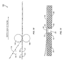
A first technique for the creation of tabs 40A, 40B is illustrated in FIGS. 6 and 7 . FIG. 6 illustrates a tab production system 130, comprising a pair of rollers 132, 134 oppositely positioned on either side of a production line 140. Top roller 132 may comprise a die cutting roller while bottom roller 134 may be a driving roller to push material though rollers 132, 134. It should be appreciated that rollers 132, 134 may be reversed if production line 140 is inverted. Production line 140 may also comprise a backing layer 142, an adhesive (not shown explicitly) and a conductive foil 144, such as a copper foil, an aluminum foil, or the like. As production line 140 passes through rollers 132, 134, die cutting roller 132 cuts conductive foil 144 into one or more tabs 40. In this particular embodiment, die cutting roller 132 cuts conductive foil 144 into two tabs 40A, 40B. Waste foil 146 is peeled from backing layer 142 while tabs 40A, 40B and backing layer 142 continue for further processing. Tabs 40 are then used to form antenna elements for antenna 60 on the wireless communication device 10 as explained below.
To accommodate substrates 20 that may have varying dielectric constants and/or thicknesses (such as may occur when switching materials having different dielectric constants forming substrate 20) variations may need to be made to the dimensions of tabs 40A, 40B to produce the optimum read range at the desired operating frequency. To ensure optimal antenna 60 performance using tabs 40A, 40B with chip 30, energy transfer should be maximized between chip 30 and tabs 40A, 40B to maximize emitted radiation from tabs 40A, 40B. To ensure maximum energy transfer, the impedance of tabs 40A, 40B must be substantially matched to the impedance of chip 30.
Further information on impedance matching between wireless communication devices and antennas is described in the previously incorporated U.S. patent application Nos. 09/678,271 and 09/678,630, and co-pending U.S. patent application No. 10/125,786 entitled “Tuning techniques for a slot antenna,” filed on Apr. 18, 2002, filed by the same assignee as that of the present application and incorporated herein by reference in its entirety.
A first technique to address this situation is illustrated in FIGS. 8 and 9 . In this technique, a plurality of rollers 200, 202, 204 is used. In particular, tab production system 130A receives production line 140. A first roller 200 makes an initial cut 206 in conductive foil 144. This initial cut 206 comprises the inner portions of tabs 40A, 40B. A second roller 202 makes a second cut 208 in conductive foil 144 that completes the creation of one of tabs 40A, 40B (in this case tab 40A). Second cut 208 overlaps to a certain extent initial cut 206 of first roller 200. A third roller 204 makes a third cut 210 in conductive foil 144 that completes the creation of the other one of tabs 40A, 40B (in this case tab 40B). Third cut 210 overlaps to a certain extent the initial cut 206 of first roller 200. Note that the precise order of the cutting by rollers 200, 202, 204 may be varied. For example, a first cut could begin on the left edge, beginning tab 40A, a second cut ends tab 40A and begins tab 40B, and the third cut ends tab 40B. Other variations are also contemplated.
The technique of FIGS. 8 and 9 allows the sizes of the tabs 40A, 40B to be varied by varying the phases of rollers 202, 204 with respect to first roller 200. Thus, if a longer tab 40A is desired, second roller 202 is phased such that there is little overlap between the cuts 206, 208. If a shorter tab 40A is desired, second roller 202 is phased such that there is substantial overlap in the cuts 206, 208. The same principle applies to the size of tab 40B, but the phase of third roller 204 is modified to achieve the desired amount of overlap between the cuts 206, 210. Allowing for differently sized tabs 40A, 40B allows optimal antenna 60 performance as previously explained. It should be appreciated that rollers 200, 202, 204 rotate at the same rate to avoid undesired phase changes between rollers 200, 202, 204. This technique is especially well suited for situations in which substrate 20 varies between wireless communication devices 10. In one embodiment, it is expected that at a 200 ft/min rate of movement of production line 120, and an antenna 60 dimension of approximately 68 mm×16 mm outside dimensions, thus giving about 60 antennas 60 per foot, approximately 12,000 antennas may be made per minute.
An alternate technique to provide variations in the size of tabs 40A, 40B is illustrated in FIGS. 10-13B . In this technique, production system 130B comprises a first roller 300 and a second roller 302, each of which is independently movable relative to one another. This technique is better suited for situations in which substrate 20 on which wireless communication device 10 is to be placed varies, as this technique allows testing on the fly to get the desired impedance for antenna 60 in conjunction with substrate 20. Rollers 300, 302 receive a production line 140A (illustrated in FIG. 13A ) comprising a backing material 130 with tabs 40A, 40B, and chip 30 disposed thereon. In contrast to the other techniques previously discussed, this technique positions, but does not specifically require, chip 30 mounted with the elements that form tabs 40.
As illustrated by the difference between FIGS. 11 and 12 , rollers 300, 302 may be spread if larger tabs 40A, 40B are required. After the testing equipment determines that the tabs 40 are appropriately sized to give the desired performance to antenna 60, a cut is made and tabs 40A, 40B are mounted on substrate 20. This cut may be made with a die, a knife, a laser, or other appropriate cutting tools (none shown). It may be desirable to test capacitance by changing one and then the other tab 40A, 40B as needed or desired. As can be seen in FIG. 13B , the cut removes tabs 40A, 40B and a portion of the backing material 130 to create hole 121, leaving tab residuals 40′, 50′.
As previously noted, some of the above techniques may be occurring concurrently with the positioning of the chips 30 on the adhesive line 118. The following section deals with mounting the chips 30 on the wireless communication device 10 after the antenna 60 has been positioned thereon.
Mounting Techniques
One technique is illustrated in FIG. 14 . In particular, a hole 22 is punched into substrate 20. Hole 22 is any type of cavity in substrate 20 or any type of geometry such that wireless communication chip 30 may be wholly or partially placed inside such cavity. Hole 22 may have tapered top edges 24 that taper from a wide opening 26 to a narrow mouth 28. The size of narrow mouth 28 may be the same or smaller in size than the width of wireless communication chip 30, so that wireless communication chip 30 rests in hole 22 at the point where narrow mouth 28 begins.
A number of techniques exist to attach chip 30 to tabs 40A, 40B. A first technique comprises using a low melting point solder. Tape ends 44, 54 of foil tape 42, 52 may be pre-loaded with a solder paste. Chip 30 is then simply dropped onto the paste (not shown), and the solder (not shown) is melted to form connectivity between tabs 40A, 40B and chip 30. Appropriate methods to form the solder joint comprise the use of infrared radiation to heat the joint locally, or pushing chip 30 into the paste with pins 32 of chip 30 preheated. Preheating of pins 32 allows the solder to remain in a liquefied state longer after initial melting so that solder may more easily flow to more surface area of tabs 40A, 40B and around pin 32 to form a stronger bond. Such preheating may be accomplished by any technique, including use of a preheating tool that emits heat such as a hot gas jet or the like.
An alternative technique for attaching chip 30 to tabs 40A, 40B comprises the use of a conductive adhesive (not shown). The adhesive forms a bond between tabs 40A, 40B and chip 30, and the conductivity of the adhesive ensures electrical continuity between tabs 40A, 40B and chip 30. Either a suitable conductive adhesive can be applied by printing to ends 44, 54 of tape 42, 52 prior to assembly, or chip 30 may be pushed onto a pressure sensitive conductive adhesive on top surfaces 46, 56 of tape 42, 52. It may be advantageous, but not required to use an adhesive that can be cured rapidly. For example, an adhesive cured by a flash of ultraviolet (IV) light would be appropriate. Examples of conductive adhesives include isotropic conductive adhesives, conductive silicones, and anisotropic conductive adhesives. The interested reader is directed to Electrically Conductive Adhesives Characteristics and Applications, a Loctite Corporation publication available at www.loctite.com that is hereby incorporated by reference in its entirety. Further information may also be found at the following website: www.chemical.felpro.com/electronics/elec_tech_index.html#eleccond.
Yet another alternative is illustrated in FIGS. 15-17 . In this embodiment, the tape 42 has one end sliced into a plurality of fingers 48. Note that the fingers 48 are made from the same material as the tape 42, but include cuts 49 between the fingers 48. The fingers are then placed proximate the hole 22. A top view of the tape 42, the fingers 48, and an exemplary positioning relative to the hole 22 is illustrated in FIG. 15 . With that arrangement in place, it is now possible to mount the chip 30.
Still another alternative would be to weld or tack pins 32 to tape 42, 52 using a suitable tool. The tool presses chip 30 into surface 21 of substrate 20. A high current may be passed through pins 32, using a low voltage pulse therethrough to form the weld. A lower voltage pulse is desirable so as to not apply a damaging voltage to chip 30. A modified chip 30 with a single thin foil (not shown) rather than multiple pins 32 may also be used for this technique. This technique may be better suited for chips 30 having an aluminum thin foil rather than a copper thin foil, since aluminum has a melting point temperature lower than copper thereby allowing use of a current that is lower in Amperes.
With all of these embodiments, a sealing layer (not shown) may also be placed onto substrate 20 and over chip 30 to hold chip 30 firmly in its desired location. This sealing layer may be an epoxy, but may instead be a robust plastic such as polyimide, Mylar, or polypropylene. These plastics may be attached by adhesives or by thermal welding as needed or desired.
It should be noted that extra layers may be added to wireless communication device 10 after or in place of the sealing layer. For example, a paper layer for printing or plastic layers may be added to the structure. Such sealing layer or layers may be applied onto substrate 20 using any type of label printing machine.
For almost any of the above styled processes, the chip 30 may be positioned on the substrate 20 with rollers as illustrated in FIGS. 18 and 19 . Chip merging system 160 is illustrated schematically in FIG. 18 and comprises a first and second heat and pressure roller 162, 164. These rollers 162, 164 may perform the thermal welding alluded to above. Adhesive line 118 with chips 30 disposed thereon passes between rollers 162, 164 and mates with substrate 20, and particularly hole 22 of substrate 20 as better seen in FIG. 19 . Tabs 40 have been prepositioned on substrate 20 prior to the introduction of the chip 30 thereto. Chip 30 may be secured to the tabs 40 and the substrate 20 by any of the means previously discussed as needed or desired.
The above-mentioned techniques are useful with a number of other manufacturing techniques. Of particular interest is the creation of tabs 40A, 40B. This may be done before, concurrently with, or after the creation of hole 22 in substrate 20 as needed or desired.
The present invention is well suited for “roll to roll” processes, making the automation of the present invention easy. As illustrated in FIG. 20 , the chip 30 positioning process may be occurring concurrently with the tab 40 creation process. The tabs are then positioned on the substrate 20 through an appropriate means as is well understood. Finally the two production lines merge and the chip 30 may be positioned on the substrate 20. Furthermore, the automation may test and mark defective parts as needed or desired.
The present invention may, of course, be carried out in other specific ways than those herein set forth without departing from the scope and the essential characteristics of the invention. The present embodiments are therefore to be construed in all aspects as illustrative and not restrictive and all changes coming within the meaning and equivalency range of the appended claims are intended to be embraced therein.
Claims (41)
1. An apparatus for producing a wireless communication device, comprising:
a cutting tool configured to cut a conductive tab for use as an antenna element, wherein the cutting tool is positionable relative to the tab to permit adjustable cutting of the tab to obtain a desired electrical characteristic for the antenna element; and
a mounting tool configured to secure a wireless communication chip to the tab and a substrate, thereby forming the wireless communication device, wherein the mounting tool includes a heater configured to heat pins of the wireless communication chip to a temperature above a yield point of the substrate so that the pins melt the substrate when inserted into the substrate.
2. The apparatus of claim 1 , wherein the cutting tool comprises:
means for adjustably cutting a first tab for use as a first antenna element; and
means for adjustably cutting a second tab for use as a second antenna element;
wherein the mounting tool further includes means for securing the first and second tabs to wireless communication chip and the substrate.
3. The apparatus of claim 2 , wherein the means for adjustably cutting the first and second tabs comprise at least two independently positionable rollers.
4. The apparatus of claim 3 , wherein the two independently positionable rollers are configured to receive a production line comprising a backing material having tabs and a wireless communication chip disposed thereon.
5. The apparatus of claim 3 , wherein the means for adjustably cutting the first and second tabs comprise cutting means to cut the backing material around the chip and through the tabs.
6. The apparatus of claim 5 , further comprising a radiator that assesses the capacitance of the first and second tabs prior to cutting to determine an appropriate size for the cut made by the cutting means.
7. The apparatus of claim 2 , wherein the means for adjustably cutting the first and second tabs comprise three rollers, each roller configured to make a cut on a production line.
8. The apparatus of claim 7 , wherein a first of the three rollers is configured to make a cut that comprises an interior portion of the first and second antenna elements.
9. The apparatus of claim 8 , wherein a second of the three rollers is configured to make a cut that comprises an exterior portion of one of the first and second antenna elements.
10. The apparatus of claim 9 , wherein a third of the three rollers is configured to make a cut that comprises an exterior portion of the other of the first and second antenna elements.
11. The apparatus of claim 7 , wherein the three rollers are phased to vary selectively the size of the first and second antenna elements.
12. The apparatus of claim 2 , wherein the means for securing the first and second tabs to the wireless communication chip comprises an adhesive.
13. The apparatus of claim 2 , wherein the means for securing the first and second tabs to the wireless communication chip comprises a hot gas jet configured to heat pins of the wireless communication chip prior to coupling to fingers cut into the first and second tabs.
14. The apparatus of claim 1 , wherein the cutting tool is further configured to receive a production line carrying a series of conductive tabs.
15. The apparatus of claim 1 , wherein the cutting tool is a first cutting tool, the apparatus further comprising a second cutting tool configured to cut a second tab for use as a second antenna element, wherein the second cutting tool is positionable relative to the second tab to permit adjustable cutting of the tab to obtain a desired electrical characteristic for the second antenna element, and wherein the mounting tool is further configured to secure the wireless communication chip to the second tab.
16. The apparatus of claim 15 , wherein the electrical characteristic is impedance, and wherein the second cutting tool is positionable to permit cutting the second tab with an impedance that matches an impedance of the wireless communication chip.
17. The apparatus of claim 1 , wherein the mounting tool is further configured to secure the wireless communication chip to the substrate via insertion of the wireless communication chip into a cavity in the substrate.
18. The apparatus of claim 17 , wherein the wireless communication chip is configured to fit inside the cavity such that a surface of the wireless communication chip is coplanar with a surface of the substrate.
19. The apparatus of claim 1 , wherein the heater is further configured to heat pins of the wireless communication chip for inserting the pins into a solder paste configured to melt and later harden to secure the wireless communication chip to the tab.
20. The apparatus of claim 19 , wherein the tab is preloaded with the solder paste.
21. The apparatus of claim 1 , wherein the mounting tool is further configured to use an adhesive to secure the wireless communication chip to the tab and the substrate.
22. The apparatus of claim 21 , wherein the adhesive is conductive.
23. The apparatus of claim 21 , wherein the adhesive is a rapidly curing adhesive.
24. The apparatus of claim 1 , wherein the heater is a hot gas jet.
25. The apparatus of claim 1 , wherein the heater is configured to heat the pins using infrared radiation.
26. The apparatus of claims 1 , wherein the tab is further configured with fingers that wrap around the pins when the pins are inserted into the substrate.
27. The apparatus of claim 1 , wherein the melted substrate forms a mechanical bond around the pins of the wireless communication chip upon cooling.
28. The apparatus of claim 1 , wherein the mounting tool further comprises a welder configured to pass a high-current, low-voltage electrical pulse through pins of the wireless communication chip to weld the pins of the wireless communication chip to the substrate.
29. The apparatus of claim 1 , wherein the mounting tool further comprises a welder configured to pass a high-current, low-voltage electrical pulse through a thin foil that melts and secures the wireless communication chip to the substrate.
30. The apparatus of claim 1 , wherein the mounting tool is further configured to place a sealing layer over the substrate and the wireless communication chip to securely hold the wireless communication chip on the substrate.
31. The apparatus of claim 30 , wherein the sealing layer comprises a plastic layer.
32. The apparatus of claim 30 , wherein the sealing layer comprises an epoxy layer.
33. The apparatus of claim 1 , wherein the electrical characteristic is impedance.
34. The apparatus of claim 33 , wherein the cutting tool is positionable to permit cutting of the first tab with an impedance that matches an impedance of the wireless communication chip.
35. The apparatus of claim 1 , wherein the electrical characteristic is capacitance.
36. The apparatus of claim 1 , wherein the electrical characteristic is configured to affect an operating frequency of the antenna element.
37. The apparatus of claim 1 , wherein the cutting tool comprises at least one of a die, a knife, or a laser.
38. An apparatus for producing a wireless communication device, comprising:
a cutting tool configured to cut a conductive tab for use as an antenna element, wherein the cutting tool is positionable relative to the tab to permit adjustable cutting of the tab to obtain a desired electrical characteristic for the antenna element; and
a mounting tool configured to secure a wireless communication chip to the tab and a substrate, thereby forming the wireless communication device, wherein the mounting tool includes a heater configured to heat pins of the wireless communication chip for inserting the pins into a solder paste configured to melt and later harden to secure the wireless communication chip to the tab.
39. The apparatus of claim 38 , wherein the tab is preloaded with the solder paste.
40. An apparatus for producing a wireless communication device, comprising:
a cutting tool configured to cut a conductive tab for use as an antenna element, wherein the cutting tool is positionable relative to the tab to permit adjustable cutting of the tab to obtain a desired electrical characteristic for the antenna element; and
a mounting tool configured to secure a wireless communication chip to the tab and a substrate, thereby forming the wireless communication device, wherein the mounting tool includes a welder configured to pass a high-current, low-voltage electrical pulse through pins of the wireless communication chip to weld the pins of the wireless communication chip to the tab.
41. An apparatus for producing a wireless communication device, comprising:
a cutting tool configured to cut a conductive tab for use as an antenna element, wherein the cutting tool is positionable relative to the tab to permit adjustable cutting of the tab to obtain a desired electrical characteristic for the antenna element; and
a mounting tool configured to secure a wireless communication chip to the tab and a substrate, thereby forming the wireless communication device, wherein the mounting tool includes a welder configured to pass a high-current, low-voltage electrical pulse through a thin foil that melts and secures the wireless communication chip to the tab.
Priority Applications (3)
| Application Number | Priority Date | Filing Date | Title |
|---|---|---|---|
| US11/468,749 US7730606B2 (en) | 2002-04-24 | 2006-08-30 | Manufacturing method for a wireless communication device and manufacturing apparatus |
| US12/782,554 US8136223B2 (en) | 2002-04-24 | 2010-05-18 | Apparatus for forming a wireless communication device |
| US13/371,019 US20120137506A1 (en) | 2002-04-24 | 2012-02-10 | Apparatus for forming a wireless communication device |
Applications Claiming Priority (3)
| Application Number | Priority Date | Filing Date | Title |
|---|---|---|---|
| US37524902P | 2002-04-24 | 2002-04-24 | |
| US10/422,616 US7191507B2 (en) | 2002-04-24 | 2003-04-24 | Method of producing a wireless communication device |
| US11/468,749 US7730606B2 (en) | 2002-04-24 | 2006-08-30 | Manufacturing method for a wireless communication device and manufacturing apparatus |
Related Parent Applications (1)
| Application Number | Title | Priority Date | Filing Date |
|---|---|---|---|
| US10/422,616 Division US7191507B2 (en) | 2002-04-24 | 2003-04-24 | Method of producing a wireless communication device |
Related Child Applications (1)
| Application Number | Title | Priority Date | Filing Date |
|---|---|---|---|
| US12/782,554 Division US8136223B2 (en) | 2002-04-24 | 2010-05-18 | Apparatus for forming a wireless communication device |
Publications (2)
| Publication Number | Publication Date |
|---|---|
| US20070060223A1 US20070060223A1 (en) | 2007-03-15 |
| US7730606B2 true US7730606B2 (en) | 2010-06-08 |
Family
ID=29270617
Family Applications (11)
| Application Number | Title | Priority Date | Filing Date |
|---|---|---|---|
| US10/422,616 Expired - Lifetime US7191507B2 (en) | 2002-04-24 | 2003-04-24 | Method of producing a wireless communication device |
| US11/468,731 Active 2024-05-22 US7647691B2 (en) | 2002-04-24 | 2006-08-30 | Method of producing antenna elements for a wireless communication device |
| US11/468,756 Expired - Lifetime US7650683B2 (en) | 2002-04-24 | 2006-08-30 | Method of preparing an antenna |
| US11/468,726 Expired - Lifetime US7546675B2 (en) | 2002-04-24 | 2006-08-30 | Method and system for manufacturing a wireless communication device |
| US11/468,749 Expired - Fee Related US7730606B2 (en) | 2002-04-24 | 2006-08-30 | Manufacturing method for a wireless communication device and manufacturing apparatus |
| US12/558,406 Expired - Lifetime US8171624B2 (en) | 2002-04-24 | 2009-09-11 | Method and system for preparing wireless communication chips for later processing |
| US12/636,136 Expired - Lifetime US8302289B2 (en) | 2002-04-24 | 2009-12-11 | Apparatus for preparing an antenna for use with a wireless communication device |
| US12/642,673 Expired - Fee Related US7908738B2 (en) | 2002-04-24 | 2009-12-18 | Apparatus for manufacturing a wireless communication device |
| US12/782,554 Expired - Fee Related US8136223B2 (en) | 2002-04-24 | 2010-05-18 | Apparatus for forming a wireless communication device |
| US13/371,019 Abandoned US20120137506A1 (en) | 2002-04-24 | 2012-02-10 | Apparatus for forming a wireless communication device |
| US13/466,969 Abandoned US20120222290A1 (en) | 2002-04-24 | 2012-05-08 | Method and system for preparing wireless communication chips for later processing |
Family Applications Before (4)
| Application Number | Title | Priority Date | Filing Date |
|---|---|---|---|
| US10/422,616 Expired - Lifetime US7191507B2 (en) | 2002-04-24 | 2003-04-24 | Method of producing a wireless communication device |
| US11/468,731 Active 2024-05-22 US7647691B2 (en) | 2002-04-24 | 2006-08-30 | Method of producing antenna elements for a wireless communication device |
| US11/468,756 Expired - Lifetime US7650683B2 (en) | 2002-04-24 | 2006-08-30 | Method of preparing an antenna |
| US11/468,726 Expired - Lifetime US7546675B2 (en) | 2002-04-24 | 2006-08-30 | Method and system for manufacturing a wireless communication device |
Family Applications After (6)
| Application Number | Title | Priority Date | Filing Date |
|---|---|---|---|
| US12/558,406 Expired - Lifetime US8171624B2 (en) | 2002-04-24 | 2009-09-11 | Method and system for preparing wireless communication chips for later processing |
| US12/636,136 Expired - Lifetime US8302289B2 (en) | 2002-04-24 | 2009-12-11 | Apparatus for preparing an antenna for use with a wireless communication device |
| US12/642,673 Expired - Fee Related US7908738B2 (en) | 2002-04-24 | 2009-12-18 | Apparatus for manufacturing a wireless communication device |
| US12/782,554 Expired - Fee Related US8136223B2 (en) | 2002-04-24 | 2010-05-18 | Apparatus for forming a wireless communication device |
| US13/371,019 Abandoned US20120137506A1 (en) | 2002-04-24 | 2012-02-10 | Apparatus for forming a wireless communication device |
| US13/466,969 Abandoned US20120222290A1 (en) | 2002-04-24 | 2012-05-08 | Method and system for preparing wireless communication chips for later processing |
Country Status (7)
| Country | Link |
|---|---|
| US (11) | US7191507B2 (en) |
| EP (2) | EP1500043B1 (en) |
| AT (2) | ATE403196T1 (en) |
| AU (1) | AU2003233033A1 (en) |
| CA (1) | CA2518614A1 (en) |
| DE (2) | DE60333409D1 (en) |
| WO (1) | WO2003092174A2 (en) |
Cited By (5)
| Publication number | Priority date | Publication date | Assignee | Title |
|---|---|---|---|---|
| US20080272885A1 (en) * | 2004-01-22 | 2008-11-06 | Mikoh Corporation | Modular Radio Frequency Identification Tagging Method |
| US20100156744A1 (en) * | 2008-12-24 | 2010-06-24 | Korea Electronics Technology Institute (A Republic Of Korea Corporation) | Antenna using buildup structure and method of manufacturing the same |
| US20100321248A1 (en) * | 2007-07-04 | 2010-12-23 | Arjowiggins Security Integrale Solutions | Fibrous substrate for insert including an antenna |
| US20110030208A1 (en) * | 2009-08-04 | 2011-02-10 | Lg Display Co., Ltd. | Apparatus and method for mounting electronic parts |
| US20120137506A1 (en) * | 2002-04-24 | 2012-06-07 | Forster Ian J | Apparatus for forming a wireless communication device |
Families Citing this family (40)
| Publication number | Priority date | Publication date | Assignee | Title |
|---|---|---|---|---|
| JP2003108961A (en) * | 2001-09-28 | 2003-04-11 | Hitachi Ltd | Electronic tag and its manufacturing method |
| US7384496B2 (en) * | 2004-02-23 | 2008-06-10 | Checkpoint Systems, Inc. | Security tag system for fabricating a tag including an integrated surface processing system |
| JP4672384B2 (en) * | 2004-04-27 | 2011-04-20 | 大日本印刷株式会社 | IC tag sheet manufacturing method, IC tag sheet manufacturing apparatus, IC tag sheet, IC chip fixing method, IC chip fixing apparatus, and IC tag |
| US7117799B2 (en) * | 2004-06-09 | 2006-10-10 | Texas Instruments Incorporated | Overhead material handling system and track block |
| US20050282355A1 (en) * | 2004-06-18 | 2005-12-22 | Edwards David N | High density bonding of electrical devices |
| US7229018B2 (en) * | 2004-08-03 | 2007-06-12 | Kurz Arthur A | Manufacture of RFID tags and intermediate products therefor |
| DE102004056238B3 (en) * | 2004-11-22 | 2006-03-30 | Arccure Technologies Gmbh | Method and arrangement for the production of RFID tags |
| US7842156B2 (en) | 2005-04-27 | 2010-11-30 | Avery Dennison Corporation | Webs and methods of making same |
| US7749350B2 (en) | 2005-04-27 | 2010-07-06 | Avery Dennison Retail Information Services | Webs and methods of making same |
| US20060290511A1 (en) * | 2005-06-22 | 2006-12-28 | Kenneth Shanton | Methods and systems for in-line RFID transponder assembly |
| US20060290512A1 (en) * | 2005-06-22 | 2006-12-28 | Smurfit-Stone Container Enterprises, Inc. | Methods and apparatus for RFID transponder fabrication |
| US7651032B2 (en) * | 2005-06-22 | 2010-01-26 | Smurfit-Stone Container Enterprises, Inc. | Methods and systems for in-line RFID transponder assembly |
| US7436305B2 (en) * | 2005-07-19 | 2008-10-14 | Checkpoint Systems, Inc. | RFID tags for pallets and cartons and system for attaching same |
| US8067253B2 (en) | 2005-12-21 | 2011-11-29 | Avery Dennison Corporation | Electrical device and method of manufacturing electrical devices using film embossing techniques to embed integrated circuits into film |
| US8786510B2 (en) * | 2006-01-24 | 2014-07-22 | Avery Dennison Corporation | Radio frequency (RF) antenna containing element and methods of making the same |
| EP2024910B1 (en) * | 2006-05-12 | 2010-11-10 | Confidex OY | A method for manufacturing products comprising transponders |
| TW200811717A (en) * | 2006-08-25 | 2008-03-01 | Advanced Connectek Inc | Method for fabricating antenna units in continuous manner |
| US20080122119A1 (en) * | 2006-08-31 | 2008-05-29 | Avery Dennison Corporation | Method and apparatus for creating rfid devices using masking techniques |
| KR100806847B1 (en) * | 2006-09-12 | 2008-02-22 | 삼성전자주식회사 | Micro antenna and its manufacturing method |
| DE102007026720A1 (en) * | 2007-06-06 | 2008-12-11 | Bielomatik Leuze Gmbh + Co.Kg | Self-adhesive antenna for an RFID system, in particular for an RFID tag, and method for its production |
| US7768407B2 (en) * | 2007-06-22 | 2010-08-03 | Avery Dennison Corporation | Foldable RFID device interposer and method |
| US7880614B2 (en) | 2007-09-26 | 2011-02-01 | Avery Dennison Corporation | RFID interposer with impedance matching |
| US8633821B2 (en) | 2007-12-03 | 2014-01-21 | Avery Dennison Corporation | Dual use RFID/EAS device |
| US8847764B2 (en) | 2007-12-05 | 2014-09-30 | Avery Dennison Corporation | RFID system with distributed read structure |
| US7786868B2 (en) * | 2007-12-11 | 2010-08-31 | Avery Dennison Corporation | RFID device with multiple passive operation modes |
| US9111191B2 (en) * | 2008-11-25 | 2015-08-18 | Avery Dennison Corporation | Method of making RFID devices |
| FR2944121B1 (en) * | 2009-04-03 | 2016-06-24 | Paragon Identification | SEMI-RIGID RADIO FREQUENCY IDENTIFICATION CARD (RFID), THE MANUFACTURING METHOD AND THE MACHINE FOR ITS MANUFACTURE |
| EP2580057B1 (en) | 2010-06-14 | 2019-05-22 | Avery Dennison Corporation | Method of manufacturing a radio frequency identification device |
| DE102010025774A1 (en) * | 2010-07-01 | 2012-01-05 | Giesecke & Devrient Gmbh | Method of making an inlay for a portable data carrier and inlay |
| FI125720B (en) | 2011-05-19 | 2016-01-29 | Tecnomar Oy | Roll-to-roll mass production method for electrical bridges |
| CN102392715B (en) * | 2011-10-11 | 2013-07-10 | 中国南方航空工业(集团)有限公司 | Oil return component of engine and engine provided with same |
| US9013365B2 (en) * | 2012-03-02 | 2015-04-21 | Harris Corporation | Interconnect feed devices for electrical components, and processes for manufacturing same |
| CA2775546A1 (en) * | 2012-04-25 | 2013-10-25 | Intelligent Devices Inc. | A disposable content use monitoring package with indicator and method of making same |
| WO2014093806A1 (en) * | 2012-12-13 | 2014-06-19 | Avery Dennison Corporation | Antenna for rfid device and method for making the same |
| WO2014144674A1 (en) * | 2013-03-15 | 2014-09-18 | Senseonics, Incorporated | Mini flat antenna system |
| WO2015131185A1 (en) * | 2014-02-28 | 2015-09-03 | Intellipaper, Llc | Integrated circuitry and methods for manufacturing same |
| US9373070B2 (en) | 2014-08-04 | 2016-06-21 | Avery Dennison Corporation | Use of RFID chip as assembly facilitator |
| WO2018012427A1 (en) | 2016-07-14 | 2018-01-18 | 株式会社村田製作所 | Attention tag for retail article and retail article having same attached thereto |
| US10320054B2 (en) | 2016-10-28 | 2019-06-11 | Avery Dennison Retail Information Services, Llc | RFID tags designed to work on difficult substrates |
| CN115209630A (en) * | 2022-07-29 | 2022-10-18 | 赛维精密科技(广东)有限公司 | Flexible printed board replacing FPCB (flexible printed circuit board) in MFA (manufacturing process of film-free adhesive) processing and process |
Citations (127)
| Publication number | Priority date | Publication date | Assignee | Title |
|---|---|---|---|---|
| US3741651A (en) | 1970-10-15 | 1973-06-26 | Matsushita Electric Ind Co Ltd | Recording device |
| US3961323A (en) | 1971-02-22 | 1976-06-01 | American Multi-Lert Corporation | Cargo monitor apparatus and method |
| US3972049A (en) | 1975-04-24 | 1976-07-27 | The United States Of America As Represented By The Secretary Of The Navy | Asymmetrically fed electric microstrip dipole antenna |
| US4051480A (en) | 1976-10-27 | 1977-09-27 | The United States Of America As Represented By The Secretary Of The Army | Conformal edge-slot radiators |
| US4086598A (en) | 1976-12-02 | 1978-04-25 | Bogner Richard D | Broadband omnidirectional slot antenna with an electrical strap connector |
| US4117489A (en) | 1975-04-24 | 1978-09-26 | The United States Of America As Represented By The Secretary Of The Navy | Corner fed electric microstrip dipole antenna |
| US4278186A (en) | 1978-09-08 | 1981-07-14 | Williamson Robert D | Method and apparatus for beverage dispensing control and quantity monitoring |
| US4433336A (en) | 1982-02-05 | 1984-02-21 | The United States Of America As Represented By The Secretary Of Commerce | Three-element antenna formed of orthogonal loops mounted on a monopole |
| US4575725A (en) | 1983-08-29 | 1986-03-11 | Allied Corporation | Double tuned, coupled microstrip antenna |
| US4587524A (en) | 1984-01-09 | 1986-05-06 | Mcdonnell Douglas Corporation | Reduced height monopole/slot antenna with offset stripline and capacitively loaded slot |
| DE3247425A1 (en) | 1982-12-22 | 1987-01-02 | Licentia Gmbh | Printed dipol antenna using stripline technology |
| US4670757A (en) | 1985-04-26 | 1987-06-02 | Eaton Corporation | Bistatic object location method |
| US4673923A (en) | 1986-05-19 | 1987-06-16 | Checkpoint Systems, Inc. | Article surveillance using reactivatable resonant tags |
| US4694283A (en) | 1981-10-30 | 1987-09-15 | Reeb Max E | Identification device in the form of a tag-like strip affixable to an article |
| US4782345A (en) | 1986-07-29 | 1988-11-01 | Amtech Corporation | Transponder antenna |
| US4846922A (en) | 1986-09-29 | 1989-07-11 | Monarch Marking Systems, Inc. | Method of making deactivatable tags |
| US4850020A (en) | 1987-11-05 | 1989-07-18 | Kahn Leonard R | Asymmetrical sideband AM stereo transmission |
| US4857893A (en) | 1986-07-18 | 1989-08-15 | Bi Inc. | Single chip transponder device |
| US4873532A (en) | 1987-10-07 | 1989-10-10 | Nippon Sheet Glass Co., Ltd. | Antenna apparatus for a vehicle |
| US4900386A (en) | 1987-05-22 | 1990-02-13 | Durgo Ag | Method of producing labels each having a circuit forming an oscillating circuit |
| US4947181A (en) | 1988-12-19 | 1990-08-07 | Raytheon Company | Asymmetrical biconical horn antenna |
| US4975711A (en) | 1988-08-31 | 1990-12-04 | Samsung Electronic Co., Ltd. | Slot antenna device for portable radiophone |
| US5006857A (en) | 1989-08-09 | 1991-04-09 | The Boeing Company | Asymmetrical triangular patch antenna element |
| US5055968A (en) | 1988-07-04 | 1991-10-08 | Sony Corporation | Thin electronic device having an integrated circuit chip and a power battery and a method for producing same |
| US5073971A (en) | 1989-09-05 | 1991-12-17 | Motorola, Inc. | Cellular radiotelephone communications system |
| US5155493A (en) | 1990-08-28 | 1992-10-13 | The United States Of America As Represented By The Secretary Of The Air Force | Tape type microstrip patch antenna |
| US5187489A (en) | 1991-08-26 | 1993-02-16 | Hughes Aircraft Company | Asymmetrically flared notch radiator |
| US5216435A (en) | 1988-10-19 | 1993-06-01 | Toyo Communication Equipment Co., Ltd. | Array antenna power supply system having power supply lines secured in a cylinder by adhesive |
| US5216430A (en) | 1990-12-27 | 1993-06-01 | General Electric Company | Low impedance printed circuit radiating element |
| US5255819A (en) | 1990-02-09 | 1993-10-26 | Peckels Arganious E | Method and apparatus for manual dispensing from discrete vessels with electronic system control and dispensing data generation on each vessel, data transmission by radio or interrogator, and remote data recording |
| US5298894A (en) | 1992-06-17 | 1994-03-29 | Badger Meter, Inc. | Utility meter transponder/antenna assembly for underground installations |
| US5315303A (en) | 1991-09-30 | 1994-05-24 | Trw Inc. | Compact, flexible and integrated millimeter wave radar sensor |
| WO1994014208A1 (en) | 1992-12-16 | 1994-06-23 | University Of Bradford | Improvements in or relating to portable phones |
| US5339074A (en) | 1991-09-13 | 1994-08-16 | Fluoroware, Inc. | Very low frequency tracking system |
| US5347280A (en) | 1993-07-02 | 1994-09-13 | Texas Instruments Deutschland Gmbh | Frequency diversity transponder arrangement |
| EP0615285A2 (en) | 1993-03-11 | 1994-09-14 | Btg International Limited | Attaching an electronic circuit to a substrate |
| US5376943A (en) | 1990-09-07 | 1994-12-27 | Plessey Semiconductors Limited | Moving vehicle transponder |
| US5381137A (en) | 1992-10-26 | 1995-01-10 | Motorola, Inc. | RF tagging system and RF tags and method |
| US5430441A (en) | 1993-10-12 | 1995-07-04 | Motorola, Inc. | Transponding tag and method |
| US5448220A (en) | 1993-04-08 | 1995-09-05 | Levy; Raymond H. | Apparatus for transmitting contents information |
| US5461393A (en) | 1993-08-20 | 1995-10-24 | Texas Instruments Incorporated | Dual frequency cavity backed slot antenna |
| US5495218A (en) | 1994-04-20 | 1996-02-27 | Thermo Instrument Controls Inc. | Microwave waveguide seal assembly |
| US5507411A (en) | 1990-02-09 | 1996-04-16 | Berg Company, A Division Of Dec International, Inc. | Electronic dispensing heads |
| US5508706A (en) | 1991-09-30 | 1996-04-16 | Trw Inc. | Radar signal processor |
| US5512901A (en) | 1991-09-30 | 1996-04-30 | Trw Inc. | Built-in radiation structure for a millimeter wave radar sensor |
| DE4446203A1 (en) | 1994-12-23 | 1996-06-27 | Hartmut Keuper | Process for digitally recording the circulation of beer kegs |
| DE19500925A1 (en) | 1995-01-16 | 1996-07-18 | Orga Kartensysteme Gmbh | Integrated circuit (I.C) card or "chip" card |
| US5539414A (en) | 1993-09-02 | 1996-07-23 | Inmarsat | Folded dipole microstrip antenna |
| US5541399A (en) | 1994-09-30 | 1996-07-30 | Palomar Technologies Corporation | RF transponder with resonant crossover antenna coil |
| US5574470A (en) | 1994-09-30 | 1996-11-12 | Palomar Technologies Corporation | Radio frequency identification transponder apparatus and method |
| US5584113A (en) | 1995-02-08 | 1996-12-17 | Hovorka; Fred D. | Method for identifying cast parts |
| US5585953A (en) | 1993-08-13 | 1996-12-17 | Gec Plessey Semiconductors, Inc. | IR/RF radio transceiver and method |
| US5592182A (en) | 1995-07-10 | 1997-01-07 | Texas Instruments Incorporated | Efficient, dual-polarization, three-dimensionally omni-directional crossed-loop antenna with a planar base element |
| US5600333A (en) | 1995-01-26 | 1997-02-04 | Larsen Electronics, Inc. | Active repeater antenna assembly |
| US5603430A (en) | 1995-02-10 | 1997-02-18 | Dec International, Inc. | Beverage dispensing system with bottle identification mechanism |
| US5621419A (en) | 1994-05-26 | 1997-04-15 | Schlumberger Industries Limited | Circular slot antenna |
| US5635917A (en) | 1992-03-31 | 1997-06-03 | Trigon Cambridge Limited | Bag including an encodable device responsive to remote interrogation and an associated fabrication method |
| US5656115A (en) | 1994-09-30 | 1997-08-12 | Mitsubishi Cable Industries, Ltd. | Method of manufacturing flat wiring body |
| US5678301A (en) | 1991-06-04 | 1997-10-21 | Micron Technology, Inc. | Method for forming an interconnect for testing unpackaged semiconductor dice |
| US5691731A (en) | 1993-06-15 | 1997-11-25 | Texas Instruments Incorporated | Closed slot antenna having outer and inner magnetic loops |
| US5764196A (en) | 1995-04-22 | 1998-06-09 | Sony Chemicals Corp. | Multiple loop antenna |
| US5774876A (en) | 1996-06-26 | 1998-06-30 | Par Government Systems Corporation | Managing assets with active electronic tags |
| EP0855675A2 (en) | 1994-09-09 | 1998-07-29 | International Business Machines Corporation | Radio frequency circuit and memory in thin flexible package |
| US5790029A (en) | 1994-08-31 | 1998-08-04 | Sensormatic Electronics Corporation | EAS tag package |
| US5814797A (en) | 1996-11-04 | 1998-09-29 | A Rifkin Co. | Transponder system for monitoring and logging depository transactions |
| US5821859A (en) | 1996-06-07 | 1998-10-13 | Ibm Corporation | Concealed magnetic ID code and antitheft tag |
| US5826175A (en) | 1995-12-07 | 1998-10-20 | Koninklijke Ptt Nederland N.V. | Active tag having one diode for modulation and demodulation |
| US5829121A (en) * | 1995-05-08 | 1998-11-03 | Antennas America, Inc. | Antenna making method |
| US5864323A (en) | 1995-12-22 | 1999-01-26 | Texas Instruments Incorporated | Ring antennas for resonant circuits |
| US5892486A (en) | 1996-10-11 | 1999-04-06 | Channel Master Llc | Broad band dipole element and array |
| US5914640A (en) | 1996-02-29 | 1999-06-22 | Texas Instruments Incorporated | Method and system for matching the input impedance of an RF amplifier an antenna to impedance |
| US5922550A (en) | 1996-12-18 | 1999-07-13 | Kimberly-Clark Worldwide, Inc. | Biosensing devices which produce diffraction images |
| US5929813A (en) | 1998-01-09 | 1999-07-27 | Nokia Mobile Phones Limited | Antenna for mobile communications device |
| US5929760A (en) | 1997-10-20 | 1999-07-27 | Escort Memory Systems | RFID conveyor antenna |
| US5929820A (en) | 1994-02-02 | 1999-07-27 | Caulfield; Michael F. | Scanning cup-dipole antenna with fixed dipole and tilting cup |
| US5936528A (en) | 1996-05-20 | 1999-08-10 | Sunny Sealing Co., Ltd. | Visually handicapped person guidance and support |
| US5945201A (en) | 1995-10-25 | 1999-08-31 | Holat; Barry | Holographic identifier for garments |
| GB2335081A (en) | 1998-03-05 | 1999-09-08 | Nec Technologies | Antenna for mobile telephones |
| US5960961A (en) | 1998-08-03 | 1999-10-05 | Tempo G | Tab means to assure ready release of singulated wafer die or integrated circuit chips packed in adhesive backed carrier tapes |
| US5973648A (en) | 1996-10-16 | 1999-10-26 | Fuba Automotive Gmbh | Radio antenna arrangement with a patch antenna for mounting on or adjacent to the windshield of a vehicle |
| US5972156A (en) | 1994-09-09 | 1999-10-26 | Intermec Ip Corp. | Method of making a radio frequency identification tag |
| US5972152A (en) * | 1997-05-16 | 1999-10-26 | Micron Communications, Inc. | Methods of fixturing flexible circuit substrates and a processing carrier, processing a flexible circuit and processing a flexible circuit substrate relative to a processing carrier |
| US5973600A (en) | 1997-09-11 | 1999-10-26 | Precision Dynamics Corporation | Laminated radio frequency identification device |
| US5995048A (en) | 1996-05-31 | 1999-11-30 | Lucent Technologies Inc. | Quarter wave patch antenna |
| WO1999065002A1 (en) | 1998-06-09 | 1999-12-16 | Motorola Inc. | Radio frequency identification tag having an article integrated antenna |
| US6008727A (en) | 1998-09-10 | 1999-12-28 | Xerox Corporation | Selectively enabled electronic tags |
| US6018324A (en) | 1996-12-20 | 2000-01-25 | Northern Telecom Limited | Omni-directional dipole antenna with a self balancing feed arrangement |
| US6018299A (en) | 1998-06-09 | 2000-01-25 | Motorola, Inc. | Radio frequency identification tag having a printed antenna and method |
| US6019865A (en) | 1998-01-21 | 2000-02-01 | Moore U.S.A. Inc. | Method of forming labels containing transponders |
| US6023244A (en) | 1997-02-14 | 2000-02-08 | Telefonaktiebolaget Lm Ericsson | Microstrip antenna having a metal frame for control of an antenna lobe |
| US6027622A (en) | 1997-05-17 | 2000-02-22 | Robert Bosch Gmbh | Sensor element |
| US6027027A (en) | 1996-05-31 | 2000-02-22 | Lucent Technologies Inc. | Luggage tag assembly |
| US6031503A (en) | 1997-02-20 | 2000-02-29 | Raytheon Company | Polarization diverse antenna for portable communication devices |
| US6043746A (en) | 1999-02-17 | 2000-03-28 | Microchip Technology Incorporated | Radio frequency identification (RFID) security tag for merchandise and method therefor |
| US6045652A (en) | 1992-06-17 | 2000-04-04 | Micron Communications, Inc. | Method of manufacturing an enclosed transceiver |
| US6054961A (en) | 1997-09-08 | 2000-04-25 | Andrew Corporation | Dual band, glass mount antenna and flexible housing therefor |
| FR2785072A1 (en) | 1998-10-23 | 2000-04-28 | St Microelectronics Sa | Flexible self-adhesive mounted IC assembly by applying double-sided adhesive film on one faces of base plate and forming groove formed in double-sided adhesive with chip arranged inside it |
| US6057803A (en) | 1996-03-19 | 2000-05-02 | Matsushita Electric Industrial, Co., Ltd. | Antenna apparatus |
| US6075493A (en) | 1997-08-11 | 2000-06-13 | Ricoh Company, Ltd. | Tapered slot antenna |
| US6082030A (en) | 1998-08-06 | 2000-07-04 | Kesselring; Valarie Lyn | Beverage can identification system |
| US6087940A (en) | 1998-07-28 | 2000-07-11 | Novavision, Inc. | Article surveillance device and method for forming |
| US6089458A (en) | 1997-10-17 | 2000-07-18 | Micron Technology, Inc. | Method of processing liquids, epoxy fabrication method, method of fabricating a radio frequency intelligent communication device, and method involving a mixture of different liquids |
| US6094173A (en) | 1997-04-18 | 2000-07-25 | Motorola, Inc. | Method and apparatus for detecting an RFID tag signal |
| US6100804A (en) | 1998-10-29 | 2000-08-08 | Intecmec Ip Corp. | Radio frequency identification system |
| US6114962A (en) | 1998-10-15 | 2000-09-05 | Intermec Ip Corp. | RF tag having strain relieved stiff substrate and hydrostatic protection for a chip mounted thereto |
| US6118426A (en) | 1995-07-20 | 2000-09-12 | E Ink Corporation | Transducers and indicators having printed displays |
| US6140966A (en) * | 1997-07-08 | 2000-10-31 | Nokia Mobile Phones Limited | Double resonance antenna structure for several frequency ranges |
| US6155098A (en) | 1998-11-13 | 2000-12-05 | General Electric Company | Dewpoint sensor |
| US6182828B1 (en) | 1996-02-19 | 2001-02-06 | Kabushiki Kaisha Toshiba | Reel tape for provisionally supporting a bare chip |
| EP1085480A1 (en) | 1999-09-14 | 2001-03-21 | Kabushiki Kaisha Miyake | Process for producing resonant tag |
| US6214444B1 (en) | 1993-12-30 | 2001-04-10 | Kabushiki Kaisha Miyake | Circuit-like metallic foil sheet and the like and processing for producing them |
| US6239765B1 (en) | 1999-02-27 | 2001-05-29 | Rangestar Wireless, Inc. | Asymmetric dipole antenna assembly |
| US6243013B1 (en) | 1999-01-08 | 2001-06-05 | Intermec Ip Corp. | Cascaded DC voltages of multiple antenna RF tag front-end circuits |
| US6243031B1 (en) | 1998-05-20 | 2001-06-05 | Marvell International Ltd. | Selectable delay circuit having immunity to variations in fabrication and operating condition for write precompensation in a read/write channel |
| US6249260B1 (en) | 1999-07-16 | 2001-06-19 | Comant Industries, Inc. | T-top antenna for omni-directional horizontally-polarized operation |
| US6259369B1 (en) | 1999-09-30 | 2001-07-10 | Moore North America, Inc. | Low cost long distance RFID reading |
| US6278413B1 (en) | 1999-03-29 | 2001-08-21 | Intermec Ip Corporation | Antenna structure for wireless communications device, such as RFID tag |
| DE10016037A1 (en) | 2000-03-31 | 2001-10-18 | Interlock Ag Schlieren | Method for producing a label or a chip card, device for carrying out the method and a label or chip card produced thereafter |
| US6305609B1 (en) | 1996-01-26 | 2001-10-23 | Infineon Technologies Ag | Data card, process for manufacturing a data card and apparatus for manufacturing a data card |
| WO2002007085A1 (en) | 2000-07-18 | 2002-01-24 | Marconi Corporation P.L.C. | Wireless communication device and method |
| US6385407B1 (en) | 1998-12-28 | 2002-05-07 | Hitachi Maxell, Ltd. | Accommodating enclosure and management system |
| US6451154B1 (en) | 2000-02-18 | 2002-09-17 | Moore North America, Inc. | RFID manufacturing concepts |
| US6538569B1 (en) | 1998-10-30 | 2003-03-25 | The Goodyear Tire & Rubber Company | Container with sensor |
| US6925701B2 (en) | 2003-03-13 | 2005-08-09 | Checkpoint Systems, Inc. | Method of making a series of resonant frequency tags |
| US7191507B2 (en) | 2002-04-24 | 2007-03-20 | Mineral Lassen Llc | Method of producing a wireless communication device |
| US7228662B1 (en) | 2003-08-07 | 2007-06-12 | John Gary K | Removable window insulator |
| US7353598B2 (en) | 2004-11-08 | 2008-04-08 | Alien Technology Corporation | Assembly comprising functional devices and method of making same |
Family Cites Families (19)
| Publication number | Priority date | Publication date | Assignee | Title |
|---|---|---|---|---|
| US4555291A (en) * | 1981-04-23 | 1985-11-26 | Minnesota Mining And Manufacturing Company | Method of constructing an LC network |
| US5292760A (en) * | 1987-12-07 | 1994-03-08 | Hoechst-Roussel Pharmaceuticals Inc. | 4-heteroaryl-1,3-benzodiazepines and 2-substituted-α-(heteroaryl)benzeneethanamines |
| FR2691563B1 (en) | 1992-05-19 | 1996-05-31 | Francois Droz | CARD COMPRISING AT LEAST ONE ELECTRONIC ELEMENT AND METHOD FOR MANUFACTURING SUCH A CARD. |
| US5837992A (en) | 1994-07-15 | 1998-11-17 | Shinko Nameplate Co., Ltd. | Memory card and its manufacturing method |
| CN1054573C (en) | 1994-09-22 | 2000-07-19 | 罗姆股份有限公司 | Non-contact type IC card and method of manufacturing same |
| KR970054817A (en) * | 1995-12-27 | 1997-07-31 | 이형도 | Duplex dielectric filter |
| US5786626A (en) * | 1996-03-25 | 1998-07-28 | Ibm Corporation | Thin radio frequency transponder with leadframe antenna structure |
| US6215401B1 (en) * | 1996-03-25 | 2001-04-10 | Intermec Ip Corp. | Non-laminated coating for radio frequency transponder (RF tag) |
| DE19758057C1 (en) * | 1997-12-29 | 1999-05-12 | Meinen Ziegel & Co Gmbh | Antenna fabrication method for IC card |
| US6395373B2 (en) * | 1998-02-11 | 2002-05-28 | Avery Dennison Corporation | Label/tag with embedded signaling device and method and apparatus for making and using |
| US6618939B2 (en) * | 1998-02-27 | 2003-09-16 | Kabushiki Kaisha Miyake | Process for producing resonant tag |
| US6628237B1 (en) | 2000-03-25 | 2003-09-30 | Marconi Communications Inc. | Remote communication using slot antenna |
| US6366468B1 (en) * | 2000-04-28 | 2002-04-02 | Hewlett-Packard Company | Self-aligned common carrier |
| US6535175B2 (en) * | 2000-06-01 | 2003-03-18 | Intermec Ip Corp. | Adjustable length antenna system for RF transponders |
| US20020018880A1 (en) * | 2000-08-01 | 2002-02-14 | Young Robert P. | Stamping foils for use in making printed circuits and radio frequency antennas |
| US6975834B1 (en) | 2000-10-03 | 2005-12-13 | Mineral Lassen Llc | Multi-band wireless communication device and method |
| DE10130428B4 (en) | 2001-06-23 | 2005-12-22 | Boehringer Ingelheim Microparts Gmbh | Method for laminar joining of bodies |
| US7127805B2 (en) * | 2002-11-20 | 2006-10-31 | Intel Corporation | Electronic device carrier and manufacturing tape |
| US7191622B1 (en) | 2004-10-20 | 2007-03-20 | Hbi Branded Apparel Enterprises, Llc | Method for knitting a design on a garment pouch |
-
2003
- 2003-04-24 AU AU2003233033A patent/AU2003233033A1/en not_active Abandoned
- 2003-04-24 EP EP20030727834 patent/EP1500043B1/en not_active Expired - Lifetime
- 2003-04-24 US US10/422,616 patent/US7191507B2/en not_active Expired - Lifetime
- 2003-04-24 DE DE60333409T patent/DE60333409D1/en not_active Expired - Lifetime
- 2003-04-24 AT AT03727834T patent/ATE403196T1/en not_active IP Right Cessation
- 2003-04-24 WO PCT/IB2003/002296 patent/WO2003092174A2/en active IP Right Grant
- 2003-04-24 CA CA002518614A patent/CA2518614A1/en not_active Abandoned
- 2003-04-24 AT AT08013406T patent/ATE474287T1/en not_active IP Right Cessation
- 2003-04-24 DE DE60322528T patent/DE60322528D1/en not_active Expired - Lifetime
- 2003-04-24 EP EP20080013406 patent/EP1978473B1/en not_active Expired - Lifetime
-
2006
- 2006-08-30 US US11/468,731 patent/US7647691B2/en active Active
- 2006-08-30 US US11/468,756 patent/US7650683B2/en not_active Expired - Lifetime
- 2006-08-30 US US11/468,726 patent/US7546675B2/en not_active Expired - Lifetime
- 2006-08-30 US US11/468,749 patent/US7730606B2/en not_active Expired - Fee Related
-
2009
- 2009-09-11 US US12/558,406 patent/US8171624B2/en not_active Expired - Lifetime
- 2009-12-11 US US12/636,136 patent/US8302289B2/en not_active Expired - Lifetime
- 2009-12-18 US US12/642,673 patent/US7908738B2/en not_active Expired - Fee Related
-
2010
- 2010-05-18 US US12/782,554 patent/US8136223B2/en not_active Expired - Fee Related
-
2012
- 2012-02-10 US US13/371,019 patent/US20120137506A1/en not_active Abandoned
- 2012-05-08 US US13/466,969 patent/US20120222290A1/en not_active Abandoned
Patent Citations (133)
| Publication number | Priority date | Publication date | Assignee | Title |
|---|---|---|---|---|
| US3741651A (en) | 1970-10-15 | 1973-06-26 | Matsushita Electric Ind Co Ltd | Recording device |
| US3961323A (en) | 1971-02-22 | 1976-06-01 | American Multi-Lert Corporation | Cargo monitor apparatus and method |
| US3972049A (en) | 1975-04-24 | 1976-07-27 | The United States Of America As Represented By The Secretary Of The Navy | Asymmetrically fed electric microstrip dipole antenna |
| US4117489A (en) | 1975-04-24 | 1978-09-26 | The United States Of America As Represented By The Secretary Of The Navy | Corner fed electric microstrip dipole antenna |
| US4051480A (en) | 1976-10-27 | 1977-09-27 | The United States Of America As Represented By The Secretary Of The Army | Conformal edge-slot radiators |
| US4086598A (en) | 1976-12-02 | 1978-04-25 | Bogner Richard D | Broadband omnidirectional slot antenna with an electrical strap connector |
| US4278186A (en) | 1978-09-08 | 1981-07-14 | Williamson Robert D | Method and apparatus for beverage dispensing control and quantity monitoring |
| US4694283A (en) | 1981-10-30 | 1987-09-15 | Reeb Max E | Identification device in the form of a tag-like strip affixable to an article |
| US4433336A (en) | 1982-02-05 | 1984-02-21 | The United States Of America As Represented By The Secretary Of Commerce | Three-element antenna formed of orthogonal loops mounted on a monopole |
| DE3247425A1 (en) | 1982-12-22 | 1987-01-02 | Licentia Gmbh | Printed dipol antenna using stripline technology |
| US4575725A (en) | 1983-08-29 | 1986-03-11 | Allied Corporation | Double tuned, coupled microstrip antenna |
| US4587524A (en) | 1984-01-09 | 1986-05-06 | Mcdonnell Douglas Corporation | Reduced height monopole/slot antenna with offset stripline and capacitively loaded slot |
| US4670757A (en) | 1985-04-26 | 1987-06-02 | Eaton Corporation | Bistatic object location method |
| US4673923A (en) | 1986-05-19 | 1987-06-16 | Checkpoint Systems, Inc. | Article surveillance using reactivatable resonant tags |
| US4857893A (en) | 1986-07-18 | 1989-08-15 | Bi Inc. | Single chip transponder device |
| US4782345A (en) | 1986-07-29 | 1988-11-01 | Amtech Corporation | Transponder antenna |
| US4846922A (en) | 1986-09-29 | 1989-07-11 | Monarch Marking Systems, Inc. | Method of making deactivatable tags |
| US4900386A (en) | 1987-05-22 | 1990-02-13 | Durgo Ag | Method of producing labels each having a circuit forming an oscillating circuit |
| US4873532A (en) | 1987-10-07 | 1989-10-10 | Nippon Sheet Glass Co., Ltd. | Antenna apparatus for a vehicle |
| US4850020A (en) | 1987-11-05 | 1989-07-18 | Kahn Leonard R | Asymmetrical sideband AM stereo transmission |
| US5055968A (en) | 1988-07-04 | 1991-10-08 | Sony Corporation | Thin electronic device having an integrated circuit chip and a power battery and a method for producing same |
| US4975711A (en) | 1988-08-31 | 1990-12-04 | Samsung Electronic Co., Ltd. | Slot antenna device for portable radiophone |
| US5216435A (en) | 1988-10-19 | 1993-06-01 | Toyo Communication Equipment Co., Ltd. | Array antenna power supply system having power supply lines secured in a cylinder by adhesive |
| US4947181A (en) | 1988-12-19 | 1990-08-07 | Raytheon Company | Asymmetrical biconical horn antenna |
| US5006857A (en) | 1989-08-09 | 1991-04-09 | The Boeing Company | Asymmetrical triangular patch antenna element |
| US5073971A (en) | 1989-09-05 | 1991-12-17 | Motorola, Inc. | Cellular radiotelephone communications system |
| US5507411A (en) | 1990-02-09 | 1996-04-16 | Berg Company, A Division Of Dec International, Inc. | Electronic dispensing heads |
| US5255819A (en) | 1990-02-09 | 1993-10-26 | Peckels Arganious E | Method and apparatus for manual dispensing from discrete vessels with electronic system control and dispensing data generation on each vessel, data transmission by radio or interrogator, and remote data recording |
| US5155493A (en) | 1990-08-28 | 1992-10-13 | The United States Of America As Represented By The Secretary Of The Air Force | Tape type microstrip patch antenna |
| US5376943A (en) | 1990-09-07 | 1994-12-27 | Plessey Semiconductors Limited | Moving vehicle transponder |
| US5216430A (en) | 1990-12-27 | 1993-06-01 | General Electric Company | Low impedance printed circuit radiating element |
| US5678301A (en) | 1991-06-04 | 1997-10-21 | Micron Technology, Inc. | Method for forming an interconnect for testing unpackaged semiconductor dice |
| US5187489A (en) | 1991-08-26 | 1993-02-16 | Hughes Aircraft Company | Asymmetrically flared notch radiator |
| US5339074A (en) | 1991-09-13 | 1994-08-16 | Fluoroware, Inc. | Very low frequency tracking system |
| US5315303A (en) | 1991-09-30 | 1994-05-24 | Trw Inc. | Compact, flexible and integrated millimeter wave radar sensor |
| US5508706A (en) | 1991-09-30 | 1996-04-16 | Trw Inc. | Radar signal processor |
| US5512901A (en) | 1991-09-30 | 1996-04-30 | Trw Inc. | Built-in radiation structure for a millimeter wave radar sensor |
| US5635917A (en) | 1992-03-31 | 1997-06-03 | Trigon Cambridge Limited | Bag including an encodable device responsive to remote interrogation and an associated fabrication method |
| US5298894A (en) | 1992-06-17 | 1994-03-29 | Badger Meter, Inc. | Utility meter transponder/antenna assembly for underground installations |
| US6045652A (en) | 1992-06-17 | 2000-04-04 | Micron Communications, Inc. | Method of manufacturing an enclosed transceiver |
| US5381137A (en) | 1992-10-26 | 1995-01-10 | Motorola, Inc. | RF tagging system and RF tags and method |
| WO1994014208A1 (en) | 1992-12-16 | 1994-06-23 | University Of Bradford | Improvements in or relating to portable phones |
| US5566441A (en) * | 1993-03-11 | 1996-10-22 | British Technology Group Limited | Attaching an electronic circuit to a substrate |
| EP0615285A2 (en) | 1993-03-11 | 1994-09-14 | Btg International Limited | Attaching an electronic circuit to a substrate |
| US5448220A (en) | 1993-04-08 | 1995-09-05 | Levy; Raymond H. | Apparatus for transmitting contents information |
| US5691731A (en) | 1993-06-15 | 1997-11-25 | Texas Instruments Incorporated | Closed slot antenna having outer and inner magnetic loops |
| US5347280A (en) | 1993-07-02 | 1994-09-13 | Texas Instruments Deutschland Gmbh | Frequency diversity transponder arrangement |
| US5585953A (en) | 1993-08-13 | 1996-12-17 | Gec Plessey Semiconductors, Inc. | IR/RF radio transceiver and method |
| US5461393A (en) | 1993-08-20 | 1995-10-24 | Texas Instruments Incorporated | Dual frequency cavity backed slot antenna |
| US5539414A (en) | 1993-09-02 | 1996-07-23 | Inmarsat | Folded dipole microstrip antenna |
| US5430441A (en) | 1993-10-12 | 1995-07-04 | Motorola, Inc. | Transponding tag and method |
| US6214444B1 (en) | 1993-12-30 | 2001-04-10 | Kabushiki Kaisha Miyake | Circuit-like metallic foil sheet and the like and processing for producing them |
| US5929820A (en) | 1994-02-02 | 1999-07-27 | Caulfield; Michael F. | Scanning cup-dipole antenna with fixed dipole and tilting cup |
| US5495218A (en) | 1994-04-20 | 1996-02-27 | Thermo Instrument Controls Inc. | Microwave waveguide seal assembly |
| US5621419A (en) | 1994-05-26 | 1997-04-15 | Schlumberger Industries Limited | Circular slot antenna |
| US5790029A (en) | 1994-08-31 | 1998-08-04 | Sensormatic Electronics Corporation | EAS tag package |
| US6078259A (en) * | 1994-09-09 | 2000-06-20 | Intermec Ip Corp. | Radio frequency identification tag |
| EP0855675A2 (en) | 1994-09-09 | 1998-07-29 | International Business Machines Corporation | Radio frequency circuit and memory in thin flexible package |
| US5972156A (en) | 1994-09-09 | 1999-10-26 | Intermec Ip Corp. | Method of making a radio frequency identification tag |
| US5656115A (en) | 1994-09-30 | 1997-08-12 | Mitsubishi Cable Industries, Ltd. | Method of manufacturing flat wiring body |
| US5541399A (en) | 1994-09-30 | 1996-07-30 | Palomar Technologies Corporation | RF transponder with resonant crossover antenna coil |
| US5574470A (en) | 1994-09-30 | 1996-11-12 | Palomar Technologies Corporation | Radio frequency identification transponder apparatus and method |
| DE4446203A1 (en) | 1994-12-23 | 1996-06-27 | Hartmut Keuper | Process for digitally recording the circulation of beer kegs |
| DE19500925A1 (en) | 1995-01-16 | 1996-07-18 | Orga Kartensysteme Gmbh | Integrated circuit (I.C) card or "chip" card |
| US5600333A (en) | 1995-01-26 | 1997-02-04 | Larsen Electronics, Inc. | Active repeater antenna assembly |
| US5584113A (en) | 1995-02-08 | 1996-12-17 | Hovorka; Fred D. | Method for identifying cast parts |
| US5603430A (en) | 1995-02-10 | 1997-02-18 | Dec International, Inc. | Beverage dispensing system with bottle identification mechanism |
| US5764196A (en) | 1995-04-22 | 1998-06-09 | Sony Chemicals Corp. | Multiple loop antenna |
| US5829121A (en) * | 1995-05-08 | 1998-11-03 | Antennas America, Inc. | Antenna making method |
| US5592182A (en) | 1995-07-10 | 1997-01-07 | Texas Instruments Incorporated | Efficient, dual-polarization, three-dimensionally omni-directional crossed-loop antenna with a planar base element |
| US6118426A (en) | 1995-07-20 | 2000-09-12 | E Ink Corporation | Transducers and indicators having printed displays |
| US6036810A (en) | 1995-10-25 | 2000-03-14 | Holat; Barry | Method of a making and applying a holographic identifier for garments |
| US5945201A (en) | 1995-10-25 | 1999-08-31 | Holat; Barry | Holographic identifier for garments |
| US5826175A (en) | 1995-12-07 | 1998-10-20 | Koninklijke Ptt Nederland N.V. | Active tag having one diode for modulation and demodulation |
| US5864323A (en) | 1995-12-22 | 1999-01-26 | Texas Instruments Incorporated | Ring antennas for resonant circuits |
| US6305609B1 (en) | 1996-01-26 | 2001-10-23 | Infineon Technologies Ag | Data card, process for manufacturing a data card and apparatus for manufacturing a data card |
| US6182828B1 (en) | 1996-02-19 | 2001-02-06 | Kabushiki Kaisha Toshiba | Reel tape for provisionally supporting a bare chip |
| US5914640A (en) | 1996-02-29 | 1999-06-22 | Texas Instruments Incorporated | Method and system for matching the input impedance of an RF amplifier an antenna to impedance |
| US6057803A (en) | 1996-03-19 | 2000-05-02 | Matsushita Electric Industrial, Co., Ltd. | Antenna apparatus |
| US5936528A (en) | 1996-05-20 | 1999-08-10 | Sunny Sealing Co., Ltd. | Visually handicapped person guidance and support |
| US5995048A (en) | 1996-05-31 | 1999-11-30 | Lucent Technologies Inc. | Quarter wave patch antenna |
| US6027027A (en) | 1996-05-31 | 2000-02-22 | Lucent Technologies Inc. | Luggage tag assembly |
| US5821859A (en) | 1996-06-07 | 1998-10-13 | Ibm Corporation | Concealed magnetic ID code and antitheft tag |
| US5774876A (en) | 1996-06-26 | 1998-06-30 | Par Government Systems Corporation | Managing assets with active electronic tags |
| US5892486A (en) | 1996-10-11 | 1999-04-06 | Channel Master Llc | Broad band dipole element and array |
| US5973648A (en) | 1996-10-16 | 1999-10-26 | Fuba Automotive Gmbh | Radio antenna arrangement with a patch antenna for mounting on or adjacent to the windshield of a vehicle |
| US5814797A (en) | 1996-11-04 | 1998-09-29 | A Rifkin Co. | Transponder system for monitoring and logging depository transactions |
| US5922550A (en) | 1996-12-18 | 1999-07-13 | Kimberly-Clark Worldwide, Inc. | Biosensing devices which produce diffraction images |
| US6018324A (en) | 1996-12-20 | 2000-01-25 | Northern Telecom Limited | Omni-directional dipole antenna with a self balancing feed arrangement |
| US6023244A (en) | 1997-02-14 | 2000-02-08 | Telefonaktiebolaget Lm Ericsson | Microstrip antenna having a metal frame for control of an antenna lobe |
| US6031503A (en) | 1997-02-20 | 2000-02-29 | Raytheon Company | Polarization diverse antenna for portable communication devices |
| US6094173A (en) | 1997-04-18 | 2000-07-25 | Motorola, Inc. | Method and apparatus for detecting an RFID tag signal |
| US5972152A (en) * | 1997-05-16 | 1999-10-26 | Micron Communications, Inc. | Methods of fixturing flexible circuit substrates and a processing carrier, processing a flexible circuit and processing a flexible circuit substrate relative to a processing carrier |
| US6027622A (en) | 1997-05-17 | 2000-02-22 | Robert Bosch Gmbh | Sensor element |
| US6140966A (en) * | 1997-07-08 | 2000-10-31 | Nokia Mobile Phones Limited | Double resonance antenna structure for several frequency ranges |
| US6075493A (en) | 1997-08-11 | 2000-06-13 | Ricoh Company, Ltd. | Tapered slot antenna |
| US6054961A (en) | 1997-09-08 | 2000-04-25 | Andrew Corporation | Dual band, glass mount antenna and flexible housing therefor |
| US5973600A (en) | 1997-09-11 | 1999-10-26 | Precision Dynamics Corporation | Laminated radio frequency identification device |
| US6089458A (en) | 1997-10-17 | 2000-07-18 | Micron Technology, Inc. | Method of processing liquids, epoxy fabrication method, method of fabricating a radio frequency intelligent communication device, and method involving a mixture of different liquids |
| US5929760A (en) | 1997-10-20 | 1999-07-27 | Escort Memory Systems | RFID conveyor antenna |
| US6025802A (en) | 1998-01-09 | 2000-02-15 | Nokia Mobile Phones Limited | Antenna for mobile communications device |
| US5929813A (en) | 1998-01-09 | 1999-07-27 | Nokia Mobile Phones Limited | Antenna for mobile communications device |
| US6019865A (en) | 1998-01-21 | 2000-02-01 | Moore U.S.A. Inc. | Method of forming labels containing transponders |
| GB2335081A (en) | 1998-03-05 | 1999-09-08 | Nec Technologies | Antenna for mobile telephones |
| US6243031B1 (en) | 1998-05-20 | 2001-06-05 | Marvell International Ltd. | Selectable delay circuit having immunity to variations in fabrication and operating condition for write precompensation in a read/write channel |
| US6018299A (en) | 1998-06-09 | 2000-01-25 | Motorola, Inc. | Radio frequency identification tag having a printed antenna and method |
| WO1999065002A1 (en) | 1998-06-09 | 1999-12-16 | Motorola Inc. | Radio frequency identification tag having an article integrated antenna |
| US6087940A (en) | 1998-07-28 | 2000-07-11 | Novavision, Inc. | Article surveillance device and method for forming |
| US5960961A (en) | 1998-08-03 | 1999-10-05 | Tempo G | Tab means to assure ready release of singulated wafer die or integrated circuit chips packed in adhesive backed carrier tapes |
| US6082030A (en) | 1998-08-06 | 2000-07-04 | Kesselring; Valarie Lyn | Beverage can identification system |
| US6008727A (en) | 1998-09-10 | 1999-12-28 | Xerox Corporation | Selectively enabled electronic tags |
| US6114962A (en) | 1998-10-15 | 2000-09-05 | Intermec Ip Corp. | RF tag having strain relieved stiff substrate and hydrostatic protection for a chip mounted thereto |
| FR2785072A1 (en) | 1998-10-23 | 2000-04-28 | St Microelectronics Sa | Flexible self-adhesive mounted IC assembly by applying double-sided adhesive film on one faces of base plate and forming groove formed in double-sided adhesive with chip arranged inside it |
| US6100804A (en) | 1998-10-29 | 2000-08-08 | Intecmec Ip Corp. | Radio frequency identification system |
| US6538569B1 (en) | 1998-10-30 | 2003-03-25 | The Goodyear Tire & Rubber Company | Container with sensor |
| US6155098A (en) | 1998-11-13 | 2000-12-05 | General Electric Company | Dewpoint sensor |
| US6385407B1 (en) | 1998-12-28 | 2002-05-07 | Hitachi Maxell, Ltd. | Accommodating enclosure and management system |
| US6243013B1 (en) | 1999-01-08 | 2001-06-05 | Intermec Ip Corp. | Cascaded DC voltages of multiple antenna RF tag front-end circuits |
| US6043746A (en) | 1999-02-17 | 2000-03-28 | Microchip Technology Incorporated | Radio frequency identification (RFID) security tag for merchandise and method therefor |
| US6239765B1 (en) | 1999-02-27 | 2001-05-29 | Rangestar Wireless, Inc. | Asymmetric dipole antenna assembly |
| US6278413B1 (en) | 1999-03-29 | 2001-08-21 | Intermec Ip Corporation | Antenna structure for wireless communications device, such as RFID tag |
| US6249260B1 (en) | 1999-07-16 | 2001-06-19 | Comant Industries, Inc. | T-top antenna for omni-directional horizontally-polarized operation |
| EP1085480A1 (en) | 1999-09-14 | 2001-03-21 | Kabushiki Kaisha Miyake | Process for producing resonant tag |
| US6259369B1 (en) | 1999-09-30 | 2001-07-10 | Moore North America, Inc. | Low cost long distance RFID reading |
| US6451154B1 (en) | 2000-02-18 | 2002-09-17 | Moore North America, Inc. | RFID manufacturing concepts |
| DE10016037A1 (en) | 2000-03-31 | 2001-10-18 | Interlock Ag Schlieren | Method for producing a label or a chip card, device for carrying out the method and a label or chip card produced thereafter |
| WO2002007085A1 (en) | 2000-07-18 | 2002-01-24 | Marconi Corporation P.L.C. | Wireless communication device and method |
| US6483473B1 (en) | 2000-07-18 | 2002-11-19 | Marconi Communications Inc. | Wireless communication device and method |
| US6853345B2 (en) | 2000-07-18 | 2005-02-08 | Marconi Intellectual Property (Us) Inc. | Wireless communication device and method |
| US7191507B2 (en) | 2002-04-24 | 2007-03-20 | Mineral Lassen Llc | Method of producing a wireless communication device |
| US6925701B2 (en) | 2003-03-13 | 2005-08-09 | Checkpoint Systems, Inc. | Method of making a series of resonant frequency tags |
| US7228662B1 (en) | 2003-08-07 | 2007-06-12 | John Gary K | Removable window insulator |
| US7353598B2 (en) | 2004-11-08 | 2008-04-08 | Alien Technology Corporation | Assembly comprising functional devices and method of making same |
Non-Patent Citations (5)
| Title |
|---|
| "AT5510 Transportation Tag," Intermec Technologies Corporation, 2 pages, Sep. 1999. |
| "BiStatix Whitepaper, Version 4.1," BiStatix Technology, [retrieved Jul. 31, 2000], pp. 1-10. |
| "BiStatix Whitepaper, Version 4.1," BiStatix Technology, <http://www.motorola.com/LMPS/Indala/bistatix.htm> [retrieved Jul. 31, 2000], pp. 1-10. |
| "Conductive Polystyrene Carrier Tape Stock," Tekpak.com, © 1998, 1999 Tek Pak Inc., 7 pages. |
| Small, D.J., and B. Eisenach, "Electrically Conductive Adhesives: Characteristics and Applications," Technical Paper, Loctite Corporation, 7 pages, Sep. 1998. |
Cited By (10)
| Publication number | Priority date | Publication date | Assignee | Title |
|---|---|---|---|---|
| US20120137506A1 (en) * | 2002-04-24 | 2012-06-07 | Forster Ian J | Apparatus for forming a wireless communication device |
| US20080272885A1 (en) * | 2004-01-22 | 2008-11-06 | Mikoh Corporation | Modular Radio Frequency Identification Tagging Method |
| US20100321248A1 (en) * | 2007-07-04 | 2010-12-23 | Arjowiggins Security Integrale Solutions | Fibrous substrate for insert including an antenna |
| US8963778B2 (en) * | 2007-07-04 | 2015-02-24 | Arjowiggins Security Integrale Solutions | Fibrous substrate for insert including an antenna |
| US20100156744A1 (en) * | 2008-12-24 | 2010-06-24 | Korea Electronics Technology Institute (A Republic Of Korea Corporation) | Antenna using buildup structure and method of manufacturing the same |
| US8350760B2 (en) * | 2008-12-24 | 2013-01-08 | Korea Electronics Technology Institute | Antenna using buildup structure and method of manufacturing the same |
| US20110030208A1 (en) * | 2009-08-04 | 2011-02-10 | Lg Display Co., Ltd. | Apparatus and method for mounting electronic parts |
| US8302290B2 (en) * | 2009-08-04 | 2012-11-06 | Lg Display Co., Ltd. | Apparatus for mounting electronic parts |
| US20130008017A1 (en) * | 2009-08-04 | 2013-01-10 | Jun-Kyu Park | Method for mounting electronic parts |
| US8528197B2 (en) * | 2009-08-04 | 2013-09-10 | Lg Display Co., Ltd. | Method for mounting electronic parts |
Also Published As
Similar Documents
| Publication | Publication Date | Title |
|---|---|---|
| US7730606B2 (en) | Manufacturing method for a wireless communication device and manufacturing apparatus | |
| US8525677B2 (en) | Blister package with integrated electronic tag and method of manufacture | |
| US7551141B1 (en) | RFID strap capacitively coupled and method of making same | |
| US7871008B2 (en) | Wireless IC device and manufacturing method thereof | |
| US8062445B2 (en) | Method of making RFID devices | |
| US7141451B2 (en) | Wireless communication medium and method of manufacturing the same | |
| US20110017833A1 (en) | RFID tag and method of manufacturing the same | |
| KR101519944B1 (en) | A method for producing an antenna element of an rfid transponder | |
| US7621043B2 (en) | Device for making an in-mold circuit | |
| MX2008000923A (en) | Rfid tags for pallets and cartons and system for attaching same. | |
| JP2018028916A (en) | Carrier tape, method for manufacturing the same, and method for manufacturing rfid tag | |
| WO2023228941A1 (en) | Electronic component module and wireless communication device comprising same | |
| JP6206626B1 (en) | Carrier tape, method for manufacturing the same, and method for manufacturing RFID tag | |
| JP2023046872A (en) | Container manufacturing method | |
| MX2008005694A (en) | Manufacturing method and device for making an in-mold circuit comprising a chip |
Legal Events
| Date | Code | Title | Description |
|---|---|---|---|
| CC | Certificate of correction | ||
| AS | Assignment |
Owner name: MINERAL LASSEN LLC, NEVADA Free format text: ASSIGNMENT OF ASSIGNORS INTEREST;ASSIGNOR:MARCONI INTELLECTUAL PROPERTY (US), INC.;REEL/FRAME:027554/0265 Effective date: 20050106 |
|
| REMI | Maintenance fee reminder mailed | ||
| LAPS | Lapse for failure to pay maintenance fees | ||
| STCH | Information on status: patent discontinuation |
Free format text: PATENT EXPIRED DUE TO NONPAYMENT OF MAINTENANCE FEES UNDER 37 CFR 1.362 |
|
| FP | Lapsed due to failure to pay maintenance fee |
Effective date: 20140608 |