US7759700B2 - Semiconductor device - Google Patents
Semiconductor device Download PDFInfo
- Publication number
- US7759700B2 US7759700B2 US11/593,016 US59301606A US7759700B2 US 7759700 B2 US7759700 B2 US 7759700B2 US 59301606 A US59301606 A US 59301606A US 7759700 B2 US7759700 B2 US 7759700B2
- Authority
- US
- United States
- Prior art keywords
- group
- iii nitride
- nitride semiconductor
- heat radiation
- semiconductor layer
- Prior art date
- Legal status (The legal status is an assumption and is not a legal conclusion. Google has not performed a legal analysis and makes no representation as to the accuracy of the status listed.)
- Active
Links
- 239000004065 semiconductor Substances 0.000 title claims abstract description 83
- 239000010410 layer Substances 0.000 claims abstract description 84
- 150000004767 nitrides Chemical class 0.000 claims abstract description 35
- 230000004888 barrier function Effects 0.000 claims abstract description 30
- 230000005855 radiation Effects 0.000 claims abstract description 30
- 239000000758 substrate Substances 0.000 claims abstract description 19
- 239000002356 single layer Substances 0.000 claims abstract description 4
- OKTJSMMVPCPJKN-UHFFFAOYSA-N Carbon Chemical compound [C] OKTJSMMVPCPJKN-UHFFFAOYSA-N 0.000 claims description 15
- 229910052799 carbon Inorganic materials 0.000 claims description 15
- 229910003460 diamond Inorganic materials 0.000 claims description 14
- 239000010432 diamond Substances 0.000 claims description 14
- 150000001875 compounds Chemical class 0.000 claims description 7
- 239000000463 material Substances 0.000 claims description 4
- CAVCGVPGBKGDTG-UHFFFAOYSA-N alumanylidynemethyl(alumanylidynemethylalumanylidenemethylidene)alumane Chemical compound [Al]#C[Al]=C=[Al]C#[Al] CAVCGVPGBKGDTG-UHFFFAOYSA-N 0.000 claims 2
- MTPVUVINMAGMJL-UHFFFAOYSA-N trimethyl(1,1,2,2,2-pentafluoroethyl)silane Chemical compound C[Si](C)(C)C(F)(F)C(F)(F)F MTPVUVINMAGMJL-UHFFFAOYSA-N 0.000 claims 2
- 238000002161 passivation Methods 0.000 abstract description 6
- 229910002601 GaN Inorganic materials 0.000 description 5
- JMASRVWKEDWRBT-UHFFFAOYSA-N Gallium nitride Chemical compound [Ga]#N JMASRVWKEDWRBT-UHFFFAOYSA-N 0.000 description 5
- RQMIWLMVTCKXAQ-UHFFFAOYSA-N [AlH3].[C] Chemical compound [AlH3].[C] RQMIWLMVTCKXAQ-UHFFFAOYSA-N 0.000 description 5
- CYKMNKXPYXUVPR-UHFFFAOYSA-N [C].[Ti] Chemical compound [C].[Ti] CYKMNKXPYXUVPR-UHFFFAOYSA-N 0.000 description 5
- 230000015556 catabolic process Effects 0.000 description 5
- 150000001722 carbon compounds Chemical class 0.000 description 4
- 230000000149 penetrating effect Effects 0.000 description 4
- -1 DLC Inorganic materials 0.000 description 3
- IJGRMHOSHXDMSA-UHFFFAOYSA-N Atomic nitrogen Chemical compound N#N IJGRMHOSHXDMSA-UHFFFAOYSA-N 0.000 description 2
- 229910052581 Si3N4 Inorganic materials 0.000 description 2
- 230000000694 effects Effects 0.000 description 2
- 230000005669 field effect Effects 0.000 description 2
- HQVNEWCFYHHQES-UHFFFAOYSA-N silicon nitride Chemical compound N12[Si]34N5[Si]62N3[Si]51N64 HQVNEWCFYHHQES-UHFFFAOYSA-N 0.000 description 2
- ZOXJGFHDIHLPTG-UHFFFAOYSA-N Boron Chemical compound [B] ZOXJGFHDIHLPTG-UHFFFAOYSA-N 0.000 description 1
- GYHNNYVSQQEPJS-UHFFFAOYSA-N Gallium Chemical compound [Ga] GYHNNYVSQQEPJS-UHFFFAOYSA-N 0.000 description 1
- 229910052782 aluminium Inorganic materials 0.000 description 1
- XAGFODPZIPBFFR-UHFFFAOYSA-N aluminium Chemical compound [Al] XAGFODPZIPBFFR-UHFFFAOYSA-N 0.000 description 1
- RNQKDQAVIXDKAG-UHFFFAOYSA-N aluminum gallium Chemical compound [Al].[Ga] RNQKDQAVIXDKAG-UHFFFAOYSA-N 0.000 description 1
- 229910052796 boron Inorganic materials 0.000 description 1
- 239000000969 carrier Substances 0.000 description 1
- 230000007547 defect Effects 0.000 description 1
- 229910052733 gallium Inorganic materials 0.000 description 1
- 239000007789 gas Substances 0.000 description 1
- 239000012535 impurity Substances 0.000 description 1
- 229910052738 indium Inorganic materials 0.000 description 1
- APFVFJFRJDLVQX-UHFFFAOYSA-N indium atom Chemical compound [In] APFVFJFRJDLVQX-UHFFFAOYSA-N 0.000 description 1
- 229910052751 metal Inorganic materials 0.000 description 1
- 239000002184 metal Substances 0.000 description 1
- 229910052757 nitrogen Inorganic materials 0.000 description 1
- 230000010287 polarization Effects 0.000 description 1
- 238000012827 research and development Methods 0.000 description 1
- 230000002269 spontaneous effect Effects 0.000 description 1
Images


Classifications
-
- H—ELECTRICITY
- H01—ELECTRIC ELEMENTS
- H01L—SEMICONDUCTOR DEVICES NOT COVERED BY CLASS H10
- H01L29/00—Semiconductor devices adapted for rectifying, amplifying, oscillating or switching, or capacitors or resistors with at least one potential-jump barrier or surface barrier, e.g. PN junction depletion layer or carrier concentration layer; Details of semiconductor bodies or of electrodes thereof ; Multistep manufacturing processes therefor
- H01L29/66—Types of semiconductor device ; Multistep manufacturing processes therefor
- H01L29/68—Types of semiconductor device ; Multistep manufacturing processes therefor controllable by only the electric current supplied, or only the electric potential applied, to an electrode which does not carry the current to be rectified, amplified or switched
- H01L29/76—Unipolar devices, e.g. field effect transistors
- H01L29/772—Field effect transistors
- H01L29/778—Field effect transistors with two-dimensional charge carrier gas channel, e.g. HEMT ; with two-dimensional charge-carrier layer formed at a heterojunction interface
- H01L29/7786—Field effect transistors with two-dimensional charge carrier gas channel, e.g. HEMT ; with two-dimensional charge-carrier layer formed at a heterojunction interface with direct single heterostructure, i.e. with wide bandgap layer formed on top of active layer, e.g. direct single heterostructure MIS-like HEMT
- H01L29/7787—Field effect transistors with two-dimensional charge carrier gas channel, e.g. HEMT ; with two-dimensional charge-carrier layer formed at a heterojunction interface with direct single heterostructure, i.e. with wide bandgap layer formed on top of active layer, e.g. direct single heterostructure MIS-like HEMT with wide bandgap charge-carrier supplying layer, e.g. direct single heterostructure MODFET
-
- H—ELECTRICITY
- H01—ELECTRIC ELEMENTS
- H01L—SEMICONDUCTOR DEVICES NOT COVERED BY CLASS H10
- H01L23/00—Details of semiconductor or other solid state devices
- H01L23/34—Arrangements for cooling, heating, ventilating or temperature compensation ; Temperature sensing arrangements
- H01L23/36—Selection of materials, or shaping, to facilitate cooling or heating, e.g. heatsinks
- H01L23/373—Cooling facilitated by selection of materials for the device or materials for thermal expansion adaptation, e.g. carbon
- H01L23/3732—Diamonds
-
- H—ELECTRICITY
- H01—ELECTRIC ELEMENTS
- H01L—SEMICONDUCTOR DEVICES NOT COVERED BY CLASS H10
- H01L29/00—Semiconductor devices adapted for rectifying, amplifying, oscillating or switching, or capacitors or resistors with at least one potential-jump barrier or surface barrier, e.g. PN junction depletion layer or carrier concentration layer; Details of semiconductor bodies or of electrodes thereof ; Multistep manufacturing processes therefor
- H01L29/66—Types of semiconductor device ; Multistep manufacturing processes therefor
- H01L29/66007—Multistep manufacturing processes
- H01L29/66075—Multistep manufacturing processes of devices having semiconductor bodies comprising group 14 or group 13/15 materials
- H01L29/66227—Multistep manufacturing processes of devices having semiconductor bodies comprising group 14 or group 13/15 materials the devices being controllable only by the electric current supplied or the electric potential applied, to an electrode which does not carry the current to be rectified, amplified or switched, e.g. three-terminal devices
- H01L29/66409—Unipolar field-effect transistors
- H01L29/66446—Unipolar field-effect transistors with an active layer made of a group 13/15 material, e.g. group 13/15 velocity modulation transistor [VMT], group 13/15 negative resistance FET [NERFET]
- H01L29/66462—Unipolar field-effect transistors with an active layer made of a group 13/15 material, e.g. group 13/15 velocity modulation transistor [VMT], group 13/15 negative resistance FET [NERFET] with a heterojunction interface channel or gate, e.g. HFET, HIGFET, SISFET, HJFET, HEMT
-
- H—ELECTRICITY
- H01—ELECTRIC ELEMENTS
- H01L—SEMICONDUCTOR DEVICES NOT COVERED BY CLASS H10
- H01L29/00—Semiconductor devices adapted for rectifying, amplifying, oscillating or switching, or capacitors or resistors with at least one potential-jump barrier or surface barrier, e.g. PN junction depletion layer or carrier concentration layer; Details of semiconductor bodies or of electrodes thereof ; Multistep manufacturing processes therefor
- H01L29/02—Semiconductor bodies ; Multistep manufacturing processes therefor
- H01L29/12—Semiconductor bodies ; Multistep manufacturing processes therefor characterised by the materials of which they are formed
- H01L29/20—Semiconductor bodies ; Multistep manufacturing processes therefor characterised by the materials of which they are formed including, apart from doping materials or other impurities, only AIIIBV compounds
- H01L29/2003—Nitride compounds
-
- H—ELECTRICITY
- H01—ELECTRIC ELEMENTS
- H01L—SEMICONDUCTOR DEVICES NOT COVERED BY CLASS H10
- H01L2924/00—Indexing scheme for arrangements or methods for connecting or disconnecting semiconductor or solid-state bodies as covered by H01L24/00
- H01L2924/0001—Technical content checked by a classifier
- H01L2924/0002—Not covered by any one of groups H01L24/00, H01L24/00 and H01L2224/00
Definitions
- the present invention relates to semiconductor devices employing a group-III nitride semiconductor.
- the present invention relates to power semiconductor devices of a group-III nitride semiconductor handling large electric power and having excellent heat radiation.
- the group-III nitride semiconductors have advantages such as wide band gap and high breakdown voltage associated with this gap, high saturation speed and high mobility of electrons, and high electron concentration in a heterojunction. Because of these advantages, research and development of the group-III nitride semiconductors is being carried out to apply them to power devices having high breakdown voltage and handling large electric power.
- FIG. 4 shows one of the most general forms of a conventional nitride semiconductor device employing a heterojunction (see, for example, Japanese Unexamined Patent Publication No. 2002-16245 or U.S. Pat. No. 6,316,793).
- an operating layer 12 of gallium nitride (GaN) and a barrier layer 13 of aluminum gallium nitride (Al x Ga 1-x N) are sequentially stacked on a substrate 11 .
- a heterojunction is formed at the interface at which the operating layer 12 and the barrier layer 13 with different band gaps are stacked.
- a source electrode 14 , a drain electrode 15 , and a gate electrode 16 are formed on the barrier layer 13 , and these electrodes operate as a heterojunction field effect transistor (abbreviated hereinafter to an HFET).
- the gate electrode 16 and the barrier layer 13 form a Schottky barrier. At the heterojunction interface between the barrier layer 13 and the operating layer 12 , electrons are accumulated at a high concentration.
- the accumulated electrons result from the difference of the amount of the spontaneous polarization and the difference of the amount of the piezo-polarization between the barrier layer 13 and the operating layer 12 , n-type impurities doped into the barrier layer 13 as appropriate, and other uncontrollable defects in the semiconductor layers, and they form a 2-dimensional electron gas (2DEG), which in turn acts as channel carriers for the field effect transistor.
- 2DEG 2-dimensional electron gas
- SiN silicon nitride
- This structure is characterized in that it includes: a conductive layer; an operating layer made of a group-III nitride semiconductor and formed above the conductive layer, a barrier layer made of a group-III nitride semiconductor and formed on the operating layer; a first source electrode, a drain electrode, and a gate electrode formed above respective portions of the barrier layer; a second source electrode connected to the first source electrode; and an interconnection member connecting the first source electrode and the conductive layer through a via hole penetrating the channel layer and the barrier layer.
- a desirable power device is a semiconductor device which has a space-saving structure and can sufficiently exert the effect of heat uniformization.
- An object of the present invention is to solve the conventional problems described above and to provide a semiconductor device using a group-III nitride semiconductor, saving space, and having a significant heat uniformization effect.
- a first semiconductor device is characterized in that the device includes: a first group-III nitride semiconductor layer formed on a substrate; a second group-III nitride semiconductor layer made of a single layer or two or more layers, formed on the first group-III nitride semiconductor layer, and acting as a barrier layer; and a source electrode, a drain electrode, and a gate electrode formed on the second group-III nitride semiconductor layer, the gate electrode controlling a current flowing between the source and drain electrodes, and as a surface passivation film, a heat radiation film with high thermal conductivity covers the entire surface other than a bonding pad.
- the group-III nitride semiconductor device capable of uniformizing its internal heat can be fabricated.
- a second semiconductor device includes: a first group-III nitride semiconductor layer formed on a substrate; a second group-III nitride semiconductor layer made of a single layer or two or more layers, formed on the first group-III nitride semiconductor layer, and acting as a barrier layer; and a first source electrode, a drain electrode, and a gate electrode formed on the second group-III nitride semiconductor layer, the gate electrode controlling a current flowing between the source and drain electrodes, the device further includes a via hole penetrating the operating layer, the barrier layer, and the substrate, and as a surface passivation film, a heat radiation film with high thermal conductivity covers the entire surface other than a bonding pad including the inside of the via hole. This is because with such a structure, the via hole can effectively uniformize heat staying ununiformly inside the semiconductor.
- the entire surface other than the bonding pad is covered with the heat radiation film as the surface passivation film having high thermal conductivity.
- the first or second semiconductor device uses, as the heat radiation film, diamond, diamond-like carbon (DLC), carbon, or a stacked film including at least two of the listed materials.
- diamond, DLC, and carbon have insulative properties and concurrently a thermal conductivity equal to or higher than metal, so that they can effectively uniformize heat staying ununiformly inside the semiconductor.
- an insulating layer different from the heat radiation film is formed between the heat radiation film and the semiconductor layer. This is because a material with high adhesion can be provided to enhance the adhesion of the heat radiation film.
- the insulating layer between the heat radiation film and the semiconductor layer is made of a compound containing carbon.
- the compound containing carbon particularly has a high adhesion to diamond, DLC, and carbon, so that the heat radiation film adheres more firmly to the semiconductor layer.
- the carbon-containing compound is titanium carbon (TiC) or aluminum carbon (AlC).
- TiC and AlC particularly has a high adhesion to diamond, DLC, and carbon, so that the heat radiation film adheres more firmly to the semiconductor layer.
- FIG. 1 is a sectional view of a semiconductor device according to a first embodiment of the present invention.
- FIGS. 2A and 2B are sectional views of a semiconductor device according to a second embodiment of the present invention.
- FIG. 3 is a sectional view of a semiconductor device according to a third embodiment of the present invention.
- FIG. 4 is a sectional view of a conventional group-III nitride semiconductor device.
- a semiconductor device according to a first embodiment of the present invention will be described with reference to FIG. 1 .
- FIG. 1 schematically shows a cross section of the semiconductor device according to the first embodiment.
- a barrier layer 13 of Al x Ga (1-x) N (0 ⁇ x ⁇ 1) is stacked on an operating layer 12 of GaN formed on a substrate 11 , and the operating layer 12 and the barrier layer 13 form a heterojunction interface.
- a source electrode 14 and a drain electrode 15 are formed away from each other, and a gate electrode 16 is formed between the source electrode 14 and the drain electrode 15 .
- Bonding pad 18 is also provided connected to the source electrode 14 and/or the drain electrode 15 .
- the surfaces of these electrodes and the barrier layer 13 are coated with an insulating film 20 made of a carbon compound (for example, titanium carbon (TiC) or aluminum carbon (AlC)) with high adhesion.
- a carbon compound for example, titanium carbon (TiC) or aluminum carbon (AlC)
- the top of the insulating film 20 is coated with a diamond film 19 having high thermal conductivity and excellent heat radiation property as a heat radiation film. It is sufficient that the insulating film 20 has such a thickness that does not block heat inside the semiconductor from transmitting into the diamond film 19 .
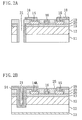
- a semiconductor device according to a second embodiment of the present invention will be described with reference to FIG. 2 .
- FIG. 2A schematically shows a cross section of the semiconductor device according to the second embodiment.
- a barrier layer 13 of Al x Ga (1-x) N (0 ⁇ x ⁇ 1) is stacked on an operating layer 12 of GaN formed on a substrate 11 , and the operating layer 12 and the barrier layer 13 form a heterojunction interface.
- a first source electrode 14 A and a drain electrode 15 are formed away from each other, and a gate electrode 16 is formed between the first source electrode 14 A and the drain electrode 15 .
- the surfaces of these electrodes and the barrier layer 13 are coated with an insulating film 20 made of a carbon compound (for example, titanium carbon (TiC) or aluminum carbon (AlC)) with high adhesion.
- a carbon compound for example, titanium carbon (TiC) or aluminum carbon (AlC)
- the top of the insulating film 20 is coated with a diamond film 19 having high thermal conductivity and excellent heat radiation property as a heat radiation film. These films also cover a via hole 21 penetrating the operating layer 12 , the barrier layer 13 , and the substrate 11 . It is sufficient that the insulating film 20 has such a thickness that does not block heat inside the semiconductor from transmitting into the diamond film 19 .
- FIG. 2B schematically shows a cross section of another semiconductor device according to the second embodiment.
- a barrier layer 13 of Al x Ga (1-x) N (0 ⁇ x ⁇ 1) is stacked on an operating layer 12 of GaN formed on, for example, a conductive Si substrate 22 , and the operating layer 12 and the barrier layer 13 form a heterojunction interface.
- a first source electrode 14 A and a drain electrode 15 are formed away from each other, and a gate electrode 16 is formed between the first source electrode 14 A and the drain electrode 15 .
- An insulating film 20 made of a carbon compound (for example, titanium carbon (TiC) or aluminum carbon (AlC)) with high adhesion is formed on the surface of the barrier layer 13 other than the electrodes 14 A, 15 and 16 .
- the top of the insulating film 20 is coated with a diamond film 19 having high thermal conductivity and excellent heat radiation property as a heat radiation film.
- the semiconductor device also includes a second source electrode 23 connected to the first source electrode 14 , and an interconnection member 24 connecting the first source electrode 14 A and the conductive substrate 22 through a via hole 21 penetrating the operating layer 12 , the barrier layer 13 , and the conductive substrate 22 .
- a diamond-like carbon (DLC) film 25 with high thermal conductivity covers the entire interconnection member 24 including the portion thereof lying inside the via hole 21 . It is sufficient that the insulating film 20 has such a thickness that does not block heat inside the semiconductor from transmitting into the diamond film 19 .
- the conductive Si substrate 22 may be any other type of semiconductor substrate, for example, SiC.
- a semiconductor device according to a third embodiment of the present invention will be described with reference to FIG. 3 .
- FIG. 3 schematically shows a cross section of the semiconductor device according to the third embodiment.
- a barrier layer 13 of Al x Ga (1-x) N (0 ⁇ x ⁇ 1) is stacked on an operating layer 12 of GaN formed on a substrate 11 , and the operating layer 12 and the barrier layer 13 form a heterojunction interface.
- a source electrode 14 On the both sides of a source electrode 14 , a pair of drain electrodes 15 are formed away from each other, and a pair of gate electrodes 16 are formed between the source electrode 14 and the pair of drain electrodes 15 , respectively.
- the surfaces of these electrodes and the barrier layer 13 are coated with an insulating film 20 made of a carbon compound (for example, titanium carbon (TiC) or aluminum carbon (AlC)) with high adhesion.
- TiC titanium carbon
- AlC aluminum carbon
- the top of the insulating film 20 is coated with a diamond film 19 having high thermal conductivity and excellent heat radiation property as a heat radiation film. It is sufficient that the insulating film 20 has such a thickness that does not block heat inside the semiconductor from transmitting into the diamond film 19 . Note that such an arrangement of the electrodes and the like may be aligned periodically multiple times.
- the entire surface is covered with the heat radiation layer with high thermal conductivity.
- the semiconductor device has a much more excellent thermal uniformity than the conventional group-III nitride semiconductor device.
- This structure eliminates an ununiform profile of heat generated in the semiconductor device during high power consumption, so that the temperature of the inside of the device is kept uniform. Therefore, the present invention is useful for a high-performance group-III nitride semiconductor device with excellent reliability, in particular for a power semiconductor device having high breakdown voltage, handling large electric power, and requiring high voltage and large current.
Abstract
Description
Claims (5)
Applications Claiming Priority (2)
| Application Number | Priority Date | Filing Date | Title |
|---|---|---|---|
| JP2005-347988 | 2005-12-01 | ||
| JP2005347988A JP2007157829A (en) | 2005-12-01 | 2005-12-01 | Semiconductor device |
Related Child Applications (1)
| Application Number | Title | Priority Date | Filing Date |
|---|---|---|---|
| US13/191,270 Continuation US8175371B2 (en) | 2004-03-16 | 2011-07-26 | Method for imaging and differential analysis of cells |
Publications (2)
| Publication Number | Publication Date |
|---|---|
| US20070126026A1 US20070126026A1 (en) | 2007-06-07 |
| US7759700B2 true US7759700B2 (en) | 2010-07-20 |
Family
ID=38117831
Family Applications (1)
| Application Number | Title | Priority Date | Filing Date |
|---|---|---|---|
| US11/593,016 Active US7759700B2 (en) | 2005-12-01 | 2006-11-06 | Semiconductor device |
Country Status (2)
| Country | Link |
|---|---|
| US (1) | US7759700B2 (en) |
| JP (1) | JP2007157829A (en) |
Cited By (32)
| Publication number | Priority date | Publication date | Assignee | Title |
|---|---|---|---|---|
| US20120038049A1 (en) * | 2008-12-16 | 2012-02-16 | Achim Trautmann | Component having a via, and a method for manufacturing such a component |
| US20120187451A1 (en) * | 2011-01-26 | 2012-07-26 | Kabushiki Kaisha Toshiba | Semiconductor element |
| US20120193677A1 (en) * | 2011-02-02 | 2012-08-02 | Transphorm Inc. | III-N Device Structures and Methods |
| US20130161692A1 (en) * | 2011-12-21 | 2013-06-27 | Alexei Koudymov | Shield wrap for a heterostructure field effect transistor |
| US8519438B2 (en) | 2008-04-23 | 2013-08-27 | Transphorm Inc. | Enhancement mode III-N HEMTs |
| US20140015136A1 (en) * | 2012-07-12 | 2014-01-16 | Zhenghao Gan | Ic device including package structure and method of forming the same |
| US8716141B2 (en) | 2011-03-04 | 2014-05-06 | Transphorm Inc. | Electrode configurations for semiconductor devices |
| US8742459B2 (en) | 2009-05-14 | 2014-06-03 | Transphorm Inc. | High voltage III-nitride semiconductor devices |
| US8742460B2 (en) | 2010-12-15 | 2014-06-03 | Transphorm Inc. | Transistors with isolation regions |
| US8772842B2 (en) | 2011-03-04 | 2014-07-08 | Transphorm, Inc. | Semiconductor diodes with low reverse bias currents |
| US8901604B2 (en) | 2011-09-06 | 2014-12-02 | Transphorm Inc. | Semiconductor devices with guard rings |
| US20150162413A1 (en) * | 2013-12-09 | 2015-06-11 | Fujitsu Limited | Semiconductor device and method of manufacturing semiconductor device |
| US9093366B2 (en) | 2012-04-09 | 2015-07-28 | Transphorm Inc. | N-polar III-nitride transistors |
| US9136347B2 (en) * | 2013-12-30 | 2015-09-15 | Electronics And Telecommunications Research Institute | Nitride semiconductor device |
| US9165766B2 (en) | 2012-02-03 | 2015-10-20 | Transphorm Inc. | Buffer layer structures suited for III-nitride devices with foreign substrates |
| US9171730B2 (en) | 2013-02-15 | 2015-10-27 | Transphorm Inc. | Electrodes for semiconductor devices and methods of forming the same |
| US9171836B2 (en) | 2011-10-07 | 2015-10-27 | Transphorm Inc. | Method of forming electronic components with increased reliability |
| US9184275B2 (en) | 2012-06-27 | 2015-11-10 | Transphorm Inc. | Semiconductor devices with integrated hole collectors |
| US9245992B2 (en) | 2013-03-15 | 2016-01-26 | Transphorm Inc. | Carbon doping semiconductor devices |
| US9257547B2 (en) | 2011-09-13 | 2016-02-09 | Transphorm Inc. | III-N device structures having a non-insulating substrate |
| US9318593B2 (en) | 2014-07-21 | 2016-04-19 | Transphorm Inc. | Forming enhancement mode III-nitride devices |
| US9443938B2 (en) | 2013-07-19 | 2016-09-13 | Transphorm Inc. | III-nitride transistor including a p-type depleting layer |
| US9536966B2 (en) | 2014-12-16 | 2017-01-03 | Transphorm Inc. | Gate structures for III-N devices |
| US9536967B2 (en) | 2014-12-16 | 2017-01-03 | Transphorm Inc. | Recessed ohmic contacts in a III-N device |
| US9559790B2 (en) | 2012-01-30 | 2017-01-31 | Keyssa, Inc. | Link emission control |
| US9590060B2 (en) | 2013-03-13 | 2017-03-07 | Transphorm Inc. | Enhancement-mode III-nitride devices |
| US9614590B2 (en) | 2011-05-12 | 2017-04-04 | Keyssa, Inc. | Scalable high-bandwidth connectivity |
| US9705204B2 (en) | 2011-10-20 | 2017-07-11 | Keyssa, Inc. | Low-profile wireless connectors |
| US9787349B2 (en) | 2011-09-15 | 2017-10-10 | Keyssa, Inc. | Wireless communication with dielectric medium |
| US10224401B2 (en) | 2016-05-31 | 2019-03-05 | Transphorm Inc. | III-nitride devices including a graded depleting layer |
| US20200006322A1 (en) * | 2018-06-29 | 2020-01-02 | Intel Corporation | Schottky diode structures and integration with iii-v transistors |
| US11322599B2 (en) | 2016-01-15 | 2022-05-03 | Transphorm Technology, Inc. | Enhancement mode III-nitride devices having an Al1-xSixO gate insulator |
Families Citing this family (20)
| Publication number | Priority date | Publication date | Assignee | Title |
|---|---|---|---|---|
| JP4945216B2 (en) * | 2006-10-30 | 2012-06-06 | 株式会社東芝 | High frequency semiconductor devices |
| EP2096675B1 (en) * | 2008-02-28 | 2013-08-21 | Universität Ulm | III-V nitride semiconductor device comprising a diamond layer |
| US7989261B2 (en) * | 2008-12-22 | 2011-08-02 | Raytheon Company | Fabricating a gallium nitride device with a diamond layer |
| US7888171B2 (en) * | 2008-12-22 | 2011-02-15 | Raytheon Company | Fabricating a gallium nitride layer with diamond layers |
| US7892881B2 (en) | 2009-02-23 | 2011-02-22 | Raytheon Company | Fabricating a device with a diamond layer |
| ES2794015T3 (en) | 2010-01-14 | 2020-11-17 | Siemens Gamesa Renewable Energy Service Gmbh | Wind turbine rotor blade components and methods for making them |
| US8835986B2 (en) * | 2011-06-22 | 2014-09-16 | Imec | Method for fabrication of III-nitride device and the III-nitride device thereof |
| KR101395026B1 (en) * | 2012-10-16 | 2014-05-15 | 경북대학교 산학협력단 | Nitride Semiconductor and Fabricating Method Thereof |
| KR101439281B1 (en) * | 2013-04-24 | 2014-09-15 | 순천대학교 산학협력단 | Heterostructure field effect transistor and its manufacturing method |
| US9362198B2 (en) | 2014-04-10 | 2016-06-07 | Freescale Semiconductor, Inc. | Semiconductor devices with a thermally conductive layer and methods of their fabrication |
| JP6174253B2 (en) * | 2014-05-26 | 2017-08-02 | シャープ株式会社 | Nitride compound semiconductor |
| CN104409431B (en) * | 2014-10-24 | 2017-07-04 | 苏州能讯高能半导体有限公司 | A kind of semiconductor devices |
| WO2017069460A2 (en) * | 2015-10-23 | 2017-04-27 | (주)기가레인 | High electron mobility transistor and manufacturing method therefor |
| CN106910724B (en) * | 2016-04-05 | 2020-06-05 | 苏州捷芯威半导体有限公司 | Semiconductor device with a plurality of transistors |
| WO2018004565A1 (en) * | 2016-06-29 | 2018-01-04 | Intel Corporation | Techniques for forming iii-n semiconductor devices with integrated diamond heat spreader |
| JP6759885B2 (en) * | 2016-09-06 | 2020-09-23 | 富士通株式会社 | Semiconductor devices and methods for manufacturing semiconductor devices |
| US10312175B1 (en) * | 2017-04-10 | 2019-06-04 | The United States Of America, As Represented By The Secretary Of The Navy | Diamond air bridge for thermal management of high power devices |
| KR102327745B1 (en) | 2018-02-01 | 2021-11-17 | 미쓰비시덴키 가부시키가이샤 | Semiconductor device and manufacturing method thereof |
| JP7139774B2 (en) | 2018-08-16 | 2022-09-21 | 富士通株式会社 | Compound semiconductor device, method for manufacturing compound semiconductor device, and amplifier |
| JP7352073B2 (en) * | 2019-08-23 | 2023-09-28 | 富士通株式会社 | Semiconductor device, semiconductor device manufacturing method, and electronic device |
Citations (13)
| Publication number | Priority date | Publication date | Assignee | Title |
|---|---|---|---|---|
| US4615102A (en) * | 1984-05-01 | 1986-10-07 | Fujitsu Limited | Method of producing enhancement mode and depletion mode FETs |
| US5225707A (en) * | 1990-06-05 | 1993-07-06 | Mitsubishi Denki Kabushiki Kaisha | Insulated via hole structure for semiconductor devices |
| US5329154A (en) * | 1992-03-17 | 1994-07-12 | Kabushiki Kaisha Toshiba | Compound semiconductor integrated circuit having improved electrode bonding arrangements |
| US6316793B1 (en) | 1998-06-12 | 2001-11-13 | Cree, Inc. | Nitride based transistors on semi-insulating silicon carbide substrates |
| JP2002016245A (en) | 2000-06-29 | 2002-01-18 | Nec Corp | Semiconductor device |
| US20030075719A1 (en) * | 2001-10-24 | 2003-04-24 | Saptharishi Sriram | Delta doped silicon carbide metal-semiconductor field effect transistors and methods of fabricating delta doped silicon carbide metal-semiconductor field effect transistors having a gate disposed in a double recess structure |
| US20040104443A1 (en) * | 2002-11-26 | 2004-06-03 | Hokyun Ahn | Semiconductor device having T-shaped gate electrode and method of manufacturing the same |
| JP2004214471A (en) * | 2003-01-07 | 2004-07-29 | Nec Corp | Field effect transistor |
| US20040224467A1 (en) * | 2003-05-09 | 2004-11-11 | Micron Technology, Inc. | Capacitor constructions |
| JP2004363563A (en) | 2003-05-15 | 2004-12-24 | Matsushita Electric Ind Co Ltd | Semiconductor device |
| US20050095842A1 (en) * | 2003-11-04 | 2005-05-05 | Semiconductor Energy Laboratory Co., Ltd. | Semiconductor device and manufacturing method thereof |
| US20060060895A1 (en) * | 2004-09-17 | 2006-03-23 | Matsushita Electric Industrial Co., Ltd. | Semiconductor device and method for fabricating the same |
| US20070176215A1 (en) * | 2006-01-27 | 2007-08-02 | Manabu Yanagihara | Transistor |
Family Cites Families (5)
| Publication number | Priority date | Publication date | Assignee | Title |
|---|---|---|---|---|
| JP2720628B2 (en) * | 1991-05-21 | 1998-03-04 | 三菱電機株式会社 | Method for manufacturing semiconductor device |
| JPH1032213A (en) * | 1996-07-17 | 1998-02-03 | Sanyo Electric Co Ltd | Semiconductor element |
| JP3241022B2 (en) * | 1999-05-25 | 2001-12-25 | 日本電気株式会社 | Field effect transistor |
| JP4336071B2 (en) * | 2001-11-08 | 2009-09-30 | 古河電気工業株式会社 | Semiconductor device with excellent heat dissipation |
| JP2005159244A (en) * | 2003-11-28 | 2005-06-16 | Matsushita Electric Ind Co Ltd | Semiconductor device |
-
2005
- 2005-12-01 JP JP2005347988A patent/JP2007157829A/en active Pending
-
2006
- 2006-11-06 US US11/593,016 patent/US7759700B2/en active Active
Patent Citations (14)
| Publication number | Priority date | Publication date | Assignee | Title |
|---|---|---|---|---|
| US4615102A (en) * | 1984-05-01 | 1986-10-07 | Fujitsu Limited | Method of producing enhancement mode and depletion mode FETs |
| US5225707A (en) * | 1990-06-05 | 1993-07-06 | Mitsubishi Denki Kabushiki Kaisha | Insulated via hole structure for semiconductor devices |
| US5329154A (en) * | 1992-03-17 | 1994-07-12 | Kabushiki Kaisha Toshiba | Compound semiconductor integrated circuit having improved electrode bonding arrangements |
| US6316793B1 (en) | 1998-06-12 | 2001-11-13 | Cree, Inc. | Nitride based transistors on semi-insulating silicon carbide substrates |
| JP2002016245A (en) | 2000-06-29 | 2002-01-18 | Nec Corp | Semiconductor device |
| US20030075719A1 (en) * | 2001-10-24 | 2003-04-24 | Saptharishi Sriram | Delta doped silicon carbide metal-semiconductor field effect transistors and methods of fabricating delta doped silicon carbide metal-semiconductor field effect transistors having a gate disposed in a double recess structure |
| US20040104443A1 (en) * | 2002-11-26 | 2004-06-03 | Hokyun Ahn | Semiconductor device having T-shaped gate electrode and method of manufacturing the same |
| JP2004214471A (en) * | 2003-01-07 | 2004-07-29 | Nec Corp | Field effect transistor |
| US20060043415A1 (en) * | 2003-01-07 | 2006-03-02 | Nec Corporation | Field-effect transistor |
| US20040224467A1 (en) * | 2003-05-09 | 2004-11-11 | Micron Technology, Inc. | Capacitor constructions |
| JP2004363563A (en) | 2003-05-15 | 2004-12-24 | Matsushita Electric Ind Co Ltd | Semiconductor device |
| US20050095842A1 (en) * | 2003-11-04 | 2005-05-05 | Semiconductor Energy Laboratory Co., Ltd. | Semiconductor device and manufacturing method thereof |
| US20060060895A1 (en) * | 2004-09-17 | 2006-03-23 | Matsushita Electric Industrial Co., Ltd. | Semiconductor device and method for fabricating the same |
| US20070176215A1 (en) * | 2006-01-27 | 2007-08-02 | Manabu Yanagihara | Transistor |
Cited By (74)
| Publication number | Priority date | Publication date | Assignee | Title |
|---|---|---|---|---|
| US9941399B2 (en) | 2008-04-23 | 2018-04-10 | Transphorm Inc. | Enhancement mode III-N HEMTs |
| US9196716B2 (en) | 2008-04-23 | 2015-11-24 | Transphorm Inc. | Enhancement mode III-N HEMTs |
| US8841702B2 (en) | 2008-04-23 | 2014-09-23 | Transphorm Inc. | Enhancement mode III-N HEMTs |
| US8519438B2 (en) | 2008-04-23 | 2013-08-27 | Transphorm Inc. | Enhancement mode III-N HEMTs |
| US9437708B2 (en) | 2008-04-23 | 2016-09-06 | Transphorm Inc. | Enhancement mode III-N HEMTs |
| US8405190B2 (en) * | 2008-12-16 | 2013-03-26 | Robert Bosch Gmbh | Component having a silicon carbide coated via |
| US20120038049A1 (en) * | 2008-12-16 | 2012-02-16 | Achim Trautmann | Component having a via, and a method for manufacturing such a component |
| US9293561B2 (en) | 2009-05-14 | 2016-03-22 | Transphorm Inc. | High voltage III-nitride semiconductor devices |
| US8742459B2 (en) | 2009-05-14 | 2014-06-03 | Transphorm Inc. | High voltage III-nitride semiconductor devices |
| US9437707B2 (en) | 2010-12-15 | 2016-09-06 | Transphorm Inc. | Transistors with isolation regions |
| US8742460B2 (en) | 2010-12-15 | 2014-06-03 | Transphorm Inc. | Transistors with isolation regions |
| US9147760B2 (en) | 2010-12-15 | 2015-09-29 | Transphorm Inc. | Transistors with isolation regions |
| US8624265B2 (en) * | 2011-01-26 | 2014-01-07 | Kabushiki Kaisha Toshiba | Semiconductor element |
| US9099564B2 (en) | 2011-01-26 | 2015-08-04 | Kabushiki Kaisha Toshiba | Nitride semiconductor element with selectively provided conductive layer under control electrode |
| US20120187451A1 (en) * | 2011-01-26 | 2012-07-26 | Kabushiki Kaisha Toshiba | Semiconductor element |
| US8643062B2 (en) * | 2011-02-02 | 2014-02-04 | Transphorm Inc. | III-N device structures and methods |
| US9224671B2 (en) | 2011-02-02 | 2015-12-29 | Transphorm Inc. | III-N device structures and methods |
| US8895421B2 (en) * | 2011-02-02 | 2014-11-25 | Transphorm Inc. | III-N device structures and methods |
| US20120193677A1 (en) * | 2011-02-02 | 2012-08-02 | Transphorm Inc. | III-N Device Structures and Methods |
| US8716141B2 (en) | 2011-03-04 | 2014-05-06 | Transphorm Inc. | Electrode configurations for semiconductor devices |
| US9142659B2 (en) | 2011-03-04 | 2015-09-22 | Transphorm Inc. | Electrode configurations for semiconductor devices |
| US8772842B2 (en) | 2011-03-04 | 2014-07-08 | Transphorm, Inc. | Semiconductor diodes with low reverse bias currents |
| US8895423B2 (en) | 2011-03-04 | 2014-11-25 | Transphorm Inc. | Method for making semiconductor diodes with low reverse bias currents |
| US11923598B2 (en) | 2011-05-12 | 2024-03-05 | Molex, Llc | Scalable high-bandwidth connectivity |
| US10601105B2 (en) | 2011-05-12 | 2020-03-24 | Keyssa, Inc. | Scalable high-bandwidth connectivity |
| US9614590B2 (en) | 2011-05-12 | 2017-04-04 | Keyssa, Inc. | Scalable high-bandwidth connectivity |
| US9224805B2 (en) | 2011-09-06 | 2015-12-29 | Transphorm Inc. | Semiconductor devices with guard rings |
| US8901604B2 (en) | 2011-09-06 | 2014-12-02 | Transphorm Inc. | Semiconductor devices with guard rings |
| US9257547B2 (en) | 2011-09-13 | 2016-02-09 | Transphorm Inc. | III-N device structures having a non-insulating substrate |
| US10027018B2 (en) | 2011-09-15 | 2018-07-17 | Keyssa, Inc. | Wireless communication with dielectric medium |
| US10707557B2 (en) | 2011-09-15 | 2020-07-07 | Keyssa, Inc. | Wireless communication with dielectric medium |
| US9787349B2 (en) | 2011-09-15 | 2017-10-10 | Keyssa, Inc. | Wireless communication with dielectric medium |
| US10381713B2 (en) | 2011-09-15 | 2019-08-13 | Keyssa, Inc. | Wireless communications with dielectric medium |
| US9171836B2 (en) | 2011-10-07 | 2015-10-27 | Transphorm Inc. | Method of forming electronic components with increased reliability |
| US9705204B2 (en) | 2011-10-20 | 2017-07-11 | Keyssa, Inc. | Low-profile wireless connectors |
| US10002957B2 (en) * | 2011-12-21 | 2018-06-19 | Power Integrations, Inc. | Shield wrap for a heterostructure field effect transistor |
| US10199488B2 (en) | 2011-12-21 | 2019-02-05 | Power Integrations, Inc. | Shield wrap for a heterostructure field effect transistor |
| US20130161692A1 (en) * | 2011-12-21 | 2013-06-27 | Alexei Koudymov | Shield wrap for a heterostructure field effect transistor |
| US9900054B2 (en) | 2012-01-30 | 2018-02-20 | Keyssa, Inc. | Link emission control |
| US10236936B2 (en) | 2012-01-30 | 2019-03-19 | Keyssa, Inc. | Link emission control |
| US9559790B2 (en) | 2012-01-30 | 2017-01-31 | Keyssa, Inc. | Link emission control |
| US9685323B2 (en) | 2012-02-03 | 2017-06-20 | Transphorm Inc. | Buffer layer structures suited for III-nitride devices with foreign substrates |
| US9165766B2 (en) | 2012-02-03 | 2015-10-20 | Transphorm Inc. | Buffer layer structures suited for III-nitride devices with foreign substrates |
| US9490324B2 (en) | 2012-04-09 | 2016-11-08 | Transphorm Inc. | N-polar III-nitride transistors |
| US9093366B2 (en) | 2012-04-09 | 2015-07-28 | Transphorm Inc. | N-polar III-nitride transistors |
| US9634100B2 (en) | 2012-06-27 | 2017-04-25 | Transphorm Inc. | Semiconductor devices with integrated hole collectors |
| US9184275B2 (en) | 2012-06-27 | 2015-11-10 | Transphorm Inc. | Semiconductor devices with integrated hole collectors |
| US20140015136A1 (en) * | 2012-07-12 | 2014-01-16 | Zhenghao Gan | Ic device including package structure and method of forming the same |
| US8816501B2 (en) * | 2012-07-12 | 2014-08-26 | Semiconductor Manufacturing International Corp | IC device including package structure and method of forming the same |
| US9520491B2 (en) | 2013-02-15 | 2016-12-13 | Transphorm Inc. | Electrodes for semiconductor devices and methods of forming the same |
| US9171730B2 (en) | 2013-02-15 | 2015-10-27 | Transphorm Inc. | Electrodes for semiconductor devices and methods of forming the same |
| US9590060B2 (en) | 2013-03-13 | 2017-03-07 | Transphorm Inc. | Enhancement-mode III-nitride devices |
| US10535763B2 (en) | 2013-03-13 | 2020-01-14 | Transphorm Inc. | Enhancement-mode III-nitride devices |
| US10043898B2 (en) | 2013-03-13 | 2018-08-07 | Transphorm Inc. | Enhancement-mode III-nitride devices |
| US9245992B2 (en) | 2013-03-15 | 2016-01-26 | Transphorm Inc. | Carbon doping semiconductor devices |
| US9865719B2 (en) | 2013-03-15 | 2018-01-09 | Transphorm Inc. | Carbon doping semiconductor devices |
| US9245993B2 (en) | 2013-03-15 | 2016-01-26 | Transphorm Inc. | Carbon doping semiconductor devices |
| US9443938B2 (en) | 2013-07-19 | 2016-09-13 | Transphorm Inc. | III-nitride transistor including a p-type depleting layer |
| US9842922B2 (en) | 2013-07-19 | 2017-12-12 | Transphorm Inc. | III-nitride transistor including a p-type depleting layer |
| US10043896B2 (en) | 2013-07-19 | 2018-08-07 | Transphorm Inc. | III-Nitride transistor including a III-N depleting layer |
| US20150162413A1 (en) * | 2013-12-09 | 2015-06-11 | Fujitsu Limited | Semiconductor device and method of manufacturing semiconductor device |
| US9966445B2 (en) | 2013-12-09 | 2018-05-08 | Fujitsu Limited | Semiconductor device and method of manufacturing semiconductor device |
| US9461135B2 (en) * | 2013-12-09 | 2016-10-04 | Fujitsu Limited | Nitride semiconductor device with multi-layer structure electrode having different work functions |
| US9136347B2 (en) * | 2013-12-30 | 2015-09-15 | Electronics And Telecommunications Research Institute | Nitride semiconductor device |
| US9318593B2 (en) | 2014-07-21 | 2016-04-19 | Transphorm Inc. | Forming enhancement mode III-nitride devices |
| US9935190B2 (en) | 2014-07-21 | 2018-04-03 | Transphorm Inc. | Forming enhancement mode III-nitride devices |
| US9536967B2 (en) | 2014-12-16 | 2017-01-03 | Transphorm Inc. | Recessed ohmic contacts in a III-N device |
| US9536966B2 (en) | 2014-12-16 | 2017-01-03 | Transphorm Inc. | Gate structures for III-N devices |
| US11322599B2 (en) | 2016-01-15 | 2022-05-03 | Transphorm Technology, Inc. | Enhancement mode III-nitride devices having an Al1-xSixO gate insulator |
| US10629681B2 (en) | 2016-05-31 | 2020-04-21 | Transphorm Technology, Inc. | III-nitride devices including a graded depleting layer |
| US11121216B2 (en) | 2016-05-31 | 2021-09-14 | Transphorm Technology, Inc. | III-nitride devices including a graded depleting layer |
| US10224401B2 (en) | 2016-05-31 | 2019-03-05 | Transphorm Inc. | III-nitride devices including a graded depleting layer |
| US20200006322A1 (en) * | 2018-06-29 | 2020-01-02 | Intel Corporation | Schottky diode structures and integration with iii-v transistors |
| US11521964B2 (en) * | 2018-06-29 | 2022-12-06 | Intel Corporation | Schottky diode structures and integration with III-V transistors |
Also Published As
| Publication number | Publication date |
|---|---|
| JP2007157829A (en) | 2007-06-21 |
| US20070126026A1 (en) | 2007-06-07 |
Similar Documents
| Publication | Publication Date | Title |
|---|---|---|
| US7759700B2 (en) | Semiconductor device | |
| US7291872B2 (en) | Semiconductor device and method for fabricating the same | |
| US7859018B2 (en) | Semiconductor device having nitride semiconductor layer | |
| US7777254B2 (en) | Normally-off field-effect semiconductor device | |
| CN100373632C (en) | Group-III nitride based high electron mobility transistor (hemt) with barrier/spacer layer | |
| US7863648B2 (en) | Field effect transistor | |
| US7859087B2 (en) | Semiconductor device | |
| US7491983B2 (en) | Nitride-based semiconductor device of reduced current leakage | |
| US8674407B2 (en) | Semiconductor device using a group III nitride-based semiconductor | |
| US20060145189A1 (en) | III-nitride power semiconductor with a field relaxation feature | |
| US20070249119A1 (en) | Nitride semiconductor device | |
| US10868164B2 (en) | Nitride semiconductor device | |
| JP2007242853A (en) | Semiconductor substrate and semiconductor device using it | |
| JP2007180143A (en) | Nitride semiconductor element | |
| JP5261923B2 (en) | Compound semiconductor device | |
| JP2007173426A (en) | Semiconductor device | |
| KR20130014861A (en) | High electron mobility transistor and method of manufacturing the same | |
| JP5553997B2 (en) | Transistor and manufacturing method thereof | |
| JP2010040828A (en) | Nitride semiconductor device | |
| US20230369479A1 (en) | Nitride-based semiconductor bidirectional switching device and method for manufacturing the same | |
| US20110062448A1 (en) | Field effect semiconductor devices and methods of manufacturing field effect semiconductor devices | |
| US8304774B2 (en) | Transistor and method for fabricating the same | |
| US20090140293A1 (en) | Heterostructure device and associated method | |
| JP2012049169A (en) | Nitride semiconductor device and method of manufacturing the same | |
| US10847620B2 (en) | Semiconductor device and method of manufacturing the same |
Legal Events
| Date | Code | Title | Description |
|---|---|---|---|
| AS | Assignment |
Owner name: MATSUSHITA ELECTRIC INDUSTRIAL CO., LTD., JAPAN Free format text: ASSIGNMENT OF ASSIGNORS INTEREST;ASSIGNORS:UENO, HIROAKI;YANAGIHARA, MANABU;UEMOTO, YASUHIRO;AND OTHERS;SIGNING DATES FROM 20061002 TO 20061011;REEL/FRAME:019152/0405 Owner name: MATSUSHITA ELECTRIC INDUSTRIAL CO., LTD., JAPAN Free format text: ASSIGNMENT OF ASSIGNORS INTEREST;ASSIGNORS:UENO, HIROAKI;YANAGIHARA, MANABU;UEMOTO, YASUHIRO;AND OTHERS;REEL/FRAME:019152/0405;SIGNING DATES FROM 20061002 TO 20061011 |
|
| AS | Assignment |
Owner name: PANASONIC CORPORATION, JAPAN Free format text: CHANGE OF NAME;ASSIGNOR:MATSUSHITA ELECTRIC INDUSTRIAL CO., LTD.;REEL/FRAME:021897/0689 Effective date: 20081001 Owner name: PANASONIC CORPORATION,JAPAN Free format text: CHANGE OF NAME;ASSIGNOR:MATSUSHITA ELECTRIC INDUSTRIAL CO., LTD.;REEL/FRAME:021897/0689 Effective date: 20081001 |
|
| STCF | Information on status: patent grant |
Free format text: PATENTED CASE |
|
| FEPP | Fee payment procedure |
Free format text: PAYOR NUMBER ASSIGNED (ORIGINAL EVENT CODE: ASPN); ENTITY STATUS OF PATENT OWNER: LARGE ENTITY |
|
| FPAY | Fee payment |
Year of fee payment: 4 |
|
| MAFP | Maintenance fee payment |
Free format text: PAYMENT OF MAINTENANCE FEE, 8TH YEAR, LARGE ENTITY (ORIGINAL EVENT CODE: M1552) Year of fee payment: 8 |
|
| MAFP | Maintenance fee payment |
Free format text: PAYMENT OF MAINTENANCE FEE, 12TH YEAR, LARGE ENTITY (ORIGINAL EVENT CODE: M1553); ENTITY STATUS OF PATENT OWNER: LARGE ENTITY Year of fee payment: 12 |