US7795091B2 - Method of forming a split gate memory device and apparatus - Google Patents
Method of forming a split gate memory device and apparatus Download PDFInfo
- Publication number
- US7795091B2 US7795091B2 US12/112,664 US11266408A US7795091B2 US 7795091 B2 US7795091 B2 US 7795091B2 US 11266408 A US11266408 A US 11266408A US 7795091 B2 US7795091 B2 US 7795091B2
- Authority
- US
- United States
- Prior art keywords
- layer
- select gate
- gate
- forming
- substrate
- Prior art date
- Legal status (The legal status is an assumption and is not a legal conclusion. Google has not performed a legal analysis and makes no representation as to the accuracy of the status listed.)
- Expired - Fee Related, expires
Links
- 238000000034 method Methods 0.000 title claims description 25
- 239000000758 substrate Substances 0.000 claims abstract description 87
- 239000000463 material Substances 0.000 claims description 75
- 239000007943 implant Substances 0.000 claims description 50
- 239000006117 anti-reflective coating Substances 0.000 claims description 32
- 239000002019 doping agent Substances 0.000 claims description 28
- 230000000903 blocking effect Effects 0.000 claims description 24
- 125000006850 spacer group Chemical group 0.000 claims description 23
- 238000005530 etching Methods 0.000 claims description 11
- 150000004767 nitrides Chemical class 0.000 claims description 5
- 239000010410 layer Substances 0.000 claims 48
- 230000006870 function Effects 0.000 abstract description 72
- 239000000969 carrier Substances 0.000 abstract description 4
- 239000004065 semiconductor Substances 0.000 description 24
- 230000015572 biosynthetic process Effects 0.000 description 10
- 229920002120 photoresistant polymer Polymers 0.000 description 8
- VYPSYNLAJGMNEJ-UHFFFAOYSA-N Silicium dioxide Chemical compound O=[Si]=O VYPSYNLAJGMNEJ-UHFFFAOYSA-N 0.000 description 4
- 229910021420 polycrystalline silicon Inorganic materials 0.000 description 4
- 229920005591 polysilicon Polymers 0.000 description 4
- XUIMIQQOPSSXEZ-UHFFFAOYSA-N Silicon Chemical compound [Si] XUIMIQQOPSSXEZ-UHFFFAOYSA-N 0.000 description 3
- 229910052710 silicon Inorganic materials 0.000 description 3
- 239000010703 silicon Substances 0.000 description 3
- 239000007787 solid Substances 0.000 description 3
- JBRZTFJDHDCESZ-UHFFFAOYSA-N AsGa Chemical compound [As]#[Ga] JBRZTFJDHDCESZ-UHFFFAOYSA-N 0.000 description 2
- 229910001218 Gallium arsenide Inorganic materials 0.000 description 2
- 229910052581 Si3N4 Inorganic materials 0.000 description 2
- NRTOMJZYCJJWKI-UHFFFAOYSA-N Titanium nitride Chemical compound [Ti]#N NRTOMJZYCJJWKI-UHFFFAOYSA-N 0.000 description 2
- 238000005468 ion implantation Methods 0.000 description 2
- 230000000873 masking effect Effects 0.000 description 2
- 238000012986 modification Methods 0.000 description 2
- 230000004048 modification Effects 0.000 description 2
- 235000012239 silicon dioxide Nutrition 0.000 description 2
- 239000000377 silicon dioxide Substances 0.000 description 2
- HQVNEWCFYHHQES-UHFFFAOYSA-N silicon nitride Chemical compound N12[Si]34N5[Si]62N3[Si]51N64 HQVNEWCFYHHQES-UHFFFAOYSA-N 0.000 description 2
- ZOXJGFHDIHLPTG-UHFFFAOYSA-N Boron Chemical compound [B] ZOXJGFHDIHLPTG-UHFFFAOYSA-N 0.000 description 1
- OAICVXFJPJFONN-UHFFFAOYSA-N Phosphorus Chemical compound [P] OAICVXFJPJFONN-UHFFFAOYSA-N 0.000 description 1
- 229910052787 antimony Inorganic materials 0.000 description 1
- WATWJIUSRGPENY-UHFFFAOYSA-N antimony atom Chemical compound [Sb] WATWJIUSRGPENY-UHFFFAOYSA-N 0.000 description 1
- 229910052785 arsenic Inorganic materials 0.000 description 1
- RQNWIZPPADIBDY-UHFFFAOYSA-N arsenic atom Chemical compound [As] RQNWIZPPADIBDY-UHFFFAOYSA-N 0.000 description 1
- 229910052796 boron Inorganic materials 0.000 description 1
- 230000000295 complement effect Effects 0.000 description 1
- 238000013500 data storage Methods 0.000 description 1
- 239000003989 dielectric material Substances 0.000 description 1
- 230000000694 effects Effects 0.000 description 1
- 230000005684 electric field Effects 0.000 description 1
- 238000005516 engineering process Methods 0.000 description 1
- 125000001475 halogen functional group Chemical group 0.000 description 1
- 229910052738 indium Inorganic materials 0.000 description 1
- APFVFJFRJDLVQX-UHFFFAOYSA-N indium atom Chemical compound [In] APFVFJFRJDLVQX-UHFFFAOYSA-N 0.000 description 1
- 239000012212 insulator Substances 0.000 description 1
- 238000002955 isolation Methods 0.000 description 1
- 229910052751 metal Inorganic materials 0.000 description 1
- 239000002184 metal Substances 0.000 description 1
- 239000002159 nanocrystal Substances 0.000 description 1
- 229910052698 phosphorus Inorganic materials 0.000 description 1
- 239000011574 phosphorus Substances 0.000 description 1
- 238000012913 prioritisation Methods 0.000 description 1
- 230000002123 temporal effect Effects 0.000 description 1
Images


Classifications
-
- H—ELECTRICITY
- H10—SEMICONDUCTOR DEVICES; ELECTRIC SOLID-STATE DEVICES NOT OTHERWISE PROVIDED FOR
- H10B—ELECTRONIC MEMORY DEVICES
- H10B43/00—EEPROM devices comprising charge-trapping gate insulators
- H10B43/40—EEPROM devices comprising charge-trapping gate insulators characterised by the peripheral circuit region
-
- H—ELECTRICITY
- H01—ELECTRIC ELEMENTS
- H01L—SEMICONDUCTOR DEVICES NOT COVERED BY CLASS H10
- H01L29/00—Semiconductor devices adapted for rectifying, amplifying, oscillating or switching, or capacitors or resistors with at least one potential-jump barrier or surface barrier, e.g. PN junction depletion layer or carrier concentration layer; Details of semiconductor bodies or of electrodes thereof ; Multistep manufacturing processes therefor
- H01L29/40—Electrodes ; Multistep manufacturing processes therefor
- H01L29/41—Electrodes ; Multistep manufacturing processes therefor characterised by their shape, relative sizes or dispositions
- H01L29/423—Electrodes ; Multistep manufacturing processes therefor characterised by their shape, relative sizes or dispositions not carrying the current to be rectified, amplified or switched
- H01L29/42312—Gate electrodes for field effect devices
- H01L29/42316—Gate electrodes for field effect devices for field-effect transistors
- H01L29/4232—Gate electrodes for field effect devices for field-effect transistors with insulated gate
- H01L29/42324—Gate electrodes for transistors with a floating gate
- H01L29/42328—Gate electrodes for transistors with a floating gate with at least one additional gate other than the floating gate and the control gate, e.g. program gate, erase gate or select gate
-
- H—ELECTRICITY
- H01—ELECTRIC ELEMENTS
- H01L—SEMICONDUCTOR DEVICES NOT COVERED BY CLASS H10
- H01L29/00—Semiconductor devices adapted for rectifying, amplifying, oscillating or switching, or capacitors or resistors with at least one potential-jump barrier or surface barrier, e.g. PN junction depletion layer or carrier concentration layer; Details of semiconductor bodies or of electrodes thereof ; Multistep manufacturing processes therefor
- H01L29/40—Electrodes ; Multistep manufacturing processes therefor
- H01L29/41—Electrodes ; Multistep manufacturing processes therefor characterised by their shape, relative sizes or dispositions
- H01L29/423—Electrodes ; Multistep manufacturing processes therefor characterised by their shape, relative sizes or dispositions not carrying the current to be rectified, amplified or switched
- H01L29/42312—Gate electrodes for field effect devices
- H01L29/42316—Gate electrodes for field effect devices for field-effect transistors
- H01L29/4232—Gate electrodes for field effect devices for field-effect transistors with insulated gate
- H01L29/42324—Gate electrodes for transistors with a floating gate
- H01L29/42332—Gate electrodes for transistors with a floating gate with the floating gate formed by two or more non connected parts, e.g. multi-particles flating gate
-
- H—ELECTRICITY
- H01—ELECTRIC ELEMENTS
- H01L—SEMICONDUCTOR DEVICES NOT COVERED BY CLASS H10
- H01L29/00—Semiconductor devices adapted for rectifying, amplifying, oscillating or switching, or capacitors or resistors with at least one potential-jump barrier or surface barrier, e.g. PN junction depletion layer or carrier concentration layer; Details of semiconductor bodies or of electrodes thereof ; Multistep manufacturing processes therefor
- H01L29/40—Electrodes ; Multistep manufacturing processes therefor
- H01L29/41—Electrodes ; Multistep manufacturing processes therefor characterised by their shape, relative sizes or dispositions
- H01L29/423—Electrodes ; Multistep manufacturing processes therefor characterised by their shape, relative sizes or dispositions not carrying the current to be rectified, amplified or switched
- H01L29/42312—Gate electrodes for field effect devices
- H01L29/42316—Gate electrodes for field effect devices for field-effect transistors
- H01L29/4232—Gate electrodes for field effect devices for field-effect transistors with insulated gate
- H01L29/4234—Gate electrodes for transistors with charge trapping gate insulator
- H01L29/42344—Gate electrodes for transistors with charge trapping gate insulator with at least one additional gate, e.g. program gate, erase gate or select gate
-
- H—ELECTRICITY
- H01—ELECTRIC ELEMENTS
- H01L—SEMICONDUCTOR DEVICES NOT COVERED BY CLASS H10
- H01L29/00—Semiconductor devices adapted for rectifying, amplifying, oscillating or switching, or capacitors or resistors with at least one potential-jump barrier or surface barrier, e.g. PN junction depletion layer or carrier concentration layer; Details of semiconductor bodies or of electrodes thereof ; Multistep manufacturing processes therefor
- H01L29/40—Electrodes ; Multistep manufacturing processes therefor
- H01L29/41—Electrodes ; Multistep manufacturing processes therefor characterised by their shape, relative sizes or dispositions
- H01L29/423—Electrodes ; Multistep manufacturing processes therefor characterised by their shape, relative sizes or dispositions not carrying the current to be rectified, amplified or switched
- H01L29/42312—Gate electrodes for field effect devices
- H01L29/42316—Gate electrodes for field effect devices for field-effect transistors
- H01L29/4232—Gate electrodes for field effect devices for field-effect transistors with insulated gate
- H01L29/4234—Gate electrodes for transistors with charge trapping gate insulator
- H01L29/42348—Gate electrodes for transistors with charge trapping gate insulator with trapping site formed by at least two separated sites, e.g. multi-particles trapping site
-
- H—ELECTRICITY
- H10—SEMICONDUCTOR DEVICES; ELECTRIC SOLID-STATE DEVICES NOT OTHERWISE PROVIDED FOR
- H10B—ELECTRONIC MEMORY DEVICES
- H10B41/00—Electrically erasable-and-programmable ROM [EEPROM] devices comprising floating gates
- H10B41/40—Electrically erasable-and-programmable ROM [EEPROM] devices comprising floating gates characterised by the peripheral circuit region
- H10B41/42—Simultaneous manufacture of periphery and memory cells
- H10B41/43—Simultaneous manufacture of periphery and memory cells comprising only one type of peripheral transistor
- H10B41/47—Simultaneous manufacture of periphery and memory cells comprising only one type of peripheral transistor with a floating-gate layer also being used as part of the peripheral transistor
Definitions
- FIGS. 1-17 illustrate in cross-sectional form a method for forming a split gate memory device in accordance with the present invention
- FIG. 3 Illustrated in FIG. 3 is further processing of semiconductor device 10 wherein a gate material layer 24 is deposited over the substrate 12 and onto each of the dielectric layer 14 and the dielectric layer 22 .
- the gate material layer 24 is a layer of polysilicon that is undoped. In other forms various materials which are conductive, or which are conductive when doped, may be used in lieu of polysilicon to implement the gate material layer 24 .
- FIG. 8 Illustrated in FIG. 8 is further processing of semiconductor device 10 wherein a mask (not shown) is provided over a portion of the ARC layer 42 where a control gate is desired to be located within the memory circuitry 13 . With the mask in place, all exposed portions of the ARC layer 42 , the gate material layer 40 and the discrete charge storage layer 36 are etched and removed. The resulting structure of FIG. 8 has a control gate 44 of N type conductivity that is formed from a remainder of the previously insitu doped N-type gate material layer 40 .
- the memory circuitry 13 thus has a memory cell having a select gate from gate material layer 24 that is doped with P conductivity and a control gate 44 that is doped with N conductivity.
- FIG. 13 Illustrated in FIG. 13 is further processing of semiconductor device 10 wherein a dopant is ion implanted into exposed regions of the substrate 12 .
- N-type dopants in the source/drain regions correspond to an N-channel memory device whereas P-type dopants in the source/drain regions correspond to a P-channel memory device.
- Deep source and drain implants are thereby performed to create a source implant region 58 and a drain implant region 60 within the other circuitry 11 . This implant also results in N-type doping of the gate 48 which is desired. Additionally formed are a source implant region 62 and a drain implant region 64 within the substrate 12 for the memory cell of the memory circuitry 13 .
- the resulting source and drain of the memory cell of memory circuitry 13 is now aligned with the overlying edges of the select gate 46 and the control gate 44 .
- the ARC layer 34 protects the underlying select gate 46 from the doping effects of the ion implantation used to form the source and drain extension implants.
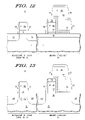
- Illustrated in FIG. 16 is further processing of semiconductor device 10 wherein the ARC layer 42 is removed from above the control gate 44 that has N conductivity. Also, exposed portions of the ARC layer 34 is removed from above the select gate 46 that has P conductivity. An unexposed portion of ARC layer 34 that underlies the discrete charge storage layer 36 is left intact. A conventional etch is used to remove the exposed portions of the ARC layer 42 and ARC layer 34 .
- the threshold voltage of the control gate is higher than the threshold voltage of the select gate in the case where the work functions of the channel regions underlying the control gate and the select gate are similar.
- the work function of the select gate is lower than the work function of the channel below it and the work function of the control gate is higher than the channel below it for the case of a substrate that is doped N-type.
- the counter doped region is formed by implanting N-type dopant species for the first majority carrier type split-gate memory device.
- the counter doped region is configured to lower the work function of the channel region.
- the counter doped region is configured to raise the work function of the channel region.
- the select gate is formed by forming a layer of select gate dielectric over at least the first portion of the substrate. A layer of select gate material is formed overlying the layer of select gate dielectric. Dopant is implanted into the layer of select gate material, wherein the dopant comprises a conductivity type suitable for establishing the first work function.
- the control gate is defined in the layer of control gate material. Defining the control gate includes etching to remove the layer of control gate material and the discrete charge storage layer in at least a region not intended for use as the control gate. A portion of the control gate overlies the second portion of the substrate.
- the implant blocking layer is a nitride antireflective coating (ARC) layer.
- ARC nitride antireflective coating
- a portion of the control gate also overlies the first edge of the select gate.
- the select gate is formed by defining a second edge of the select gate.
- a control gate is formed having a second work function overlying a second portion of the substrate proximate the first portion.
- the first work function is greater than the second work function.
- the second majority carrier type split-gate memory device wherein the second majority carrier type comprises holes, the first work function is less than the second work function.
- a first current electrode is formed in the substrate.
- a second current electrode is formed in the substrate separated from the first current electrode by a channel underlying the control gate and select gate.
- the select gate is formed by forming an implant blocking layer overlying the layer of select gate material.
- a first edge of the select gate is defined in the layer of select gate material, wherein defining the first edge includes etching to remove the implant blocking layer, the layer of select gate material and the layer of select gate dielectric in at least a region overlying the second portion of the substrate intended for use with respect to the control gate.
- the control gate in one form is formed by forming a discrete charge storage layer overlying (i) the implant blocking layer, (ii) the layer of select gate material, (iii) the first edge of the select gate, and (iv) a surface of the substrate exposed by defining the first edge of the select gate.
- a layer of control gate material is formed overlying the discrete charge storage layer.
- the control gate is defined in the layer of control gate material by etching to remove the layer of control gate material and the discrete charge storage layer in at least a region not intended for use as the control gate. A portion of the control gate overlies the second portion of the substrate.
- a split-gate memory device having a select gate having a first work function overlying a first portion of a substrate.
- a control gate has a second work function overlying a second portion of the substrate proximate the first portion, wherein (i) for a first majority carrier type split-gate memory device, wherein the first majority carrier type comprises electrons, the first work function is greater than the second work function and (ii) for a second majority carrier type split-gate memory device, wherein the second majority carrier type comprises holes, the first work function is less than the second work function.
- a first current electrode in the substrate and a second current electrode in the substrate is separated from the first current electrode by a channel underlying the control gate and select gate.
Abstract
Description
Claims (16)
Priority Applications (4)
| Application Number | Priority Date | Filing Date | Title |
|---|---|---|---|
| US12/112,664 US7795091B2 (en) | 2008-04-30 | 2008-04-30 | Method of forming a split gate memory device and apparatus |
| JP2011507498A JP2011519489A (en) | 2008-04-30 | 2009-02-26 | Method and apparatus for forming split gate memory device |
| PCT/US2009/035299 WO2009154813A2 (en) | 2008-04-30 | 2009-02-26 | Method of forming a split gate memory device and apparatus |
| TW098107107A TW200947627A (en) | 2008-04-30 | 2009-03-05 | Method of forming a split gate memory device and apparatus |
Applications Claiming Priority (1)
| Application Number | Priority Date | Filing Date | Title |
|---|---|---|---|
| US12/112,664 US7795091B2 (en) | 2008-04-30 | 2008-04-30 | Method of forming a split gate memory device and apparatus |
Publications (2)
| Publication Number | Publication Date |
|---|---|
| US20090273013A1 US20090273013A1 (en) | 2009-11-05 |
| US7795091B2 true US7795091B2 (en) | 2010-09-14 |
Family
ID=41256537
Family Applications (1)
| Application Number | Title | Priority Date | Filing Date |
|---|---|---|---|
| US12/112,664 Expired - Fee Related US7795091B2 (en) | 2008-04-30 | 2008-04-30 | Method of forming a split gate memory device and apparatus |
Country Status (4)
| Country | Link |
|---|---|
| US (1) | US7795091B2 (en) |
| JP (1) | JP2011519489A (en) |
| TW (1) | TW200947627A (en) |
| WO (1) | WO2009154813A2 (en) |
Cited By (38)
| Publication number | Priority date | Publication date | Assignee | Title |
|---|---|---|---|---|
| US20110207274A1 (en) * | 2010-02-22 | 2011-08-25 | Kang Sung-Taeg | Method for forming a split-gate memory cell |
| US8524557B1 (en) | 2012-02-22 | 2013-09-03 | Freescale Semiconductor, Inc. | Integration technique using thermal oxide select gate dielectric for select gate and replacement gate for logic |
| US8530950B1 (en) * | 2012-05-31 | 2013-09-10 | Freescale Semiconductor, Inc. | Methods and structures for split gate memory |
| US20130264633A1 (en) * | 2012-04-09 | 2013-10-10 | Mark D. Hall | Logic transistor and non-volatile memory cell integration |
| US8658497B2 (en) | 2012-01-04 | 2014-02-25 | Freescale Semiconductor, Inc. | Non-volatile memory (NVM) and logic integration |
| US8669158B2 (en) | 2012-01-04 | 2014-03-11 | Mark D. Hall | Non-volatile memory (NVM) and logic integration |
| US8716089B1 (en) | 2013-03-08 | 2014-05-06 | Freescale Semiconductor, Inc. | Integrating formation of a replacement gate transistor and a non-volatile memory cell having thin film storage |
| US8728886B2 (en) | 2012-06-08 | 2014-05-20 | Freescale Semiconductor, Inc. | Integrating formation of a replacement gate transistor and a non-volatile memory cell using a high-k dielectric |
| US8741719B1 (en) | 2013-03-08 | 2014-06-03 | Freescale Semiconductor, Inc. | Integrating formation of a logic transistor and a non-volatile memory cell using a partial replacement gate technique |
| US8797800B1 (en) | 2013-04-02 | 2014-08-05 | Sandisk Technologies Inc. | Select gate materials having different work functions in non-volatile memory |
| US8871598B1 (en) | 2013-07-31 | 2014-10-28 | Freescale Semiconductor, Inc. | Non-volatile memory (NVM) and high-k and metal gate integration using gate-first methodology |
| US8877585B1 (en) | 2013-08-16 | 2014-11-04 | Freescale Semiconductor, Inc. | Non-volatile memory (NVM) cell, high voltage transistor, and high-K and metal gate transistor integration |
| US8877568B2 (en) | 2010-10-29 | 2014-11-04 | Freescale Semiconductor, Inc. | Methods of making logic transistors and non-volatile memory cells |
| US8901632B1 (en) | 2013-09-30 | 2014-12-02 | Freescale Semiconductor, Inc. | Non-volatile memory (NVM) and high-K and metal gate integration using gate-last methodology |
| US8906764B2 (en) | 2012-01-04 | 2014-12-09 | Freescale Semiconductor, Inc. | Non-volatile memory (NVM) and logic integration |
| US8932925B1 (en) | 2013-08-22 | 2015-01-13 | Freescale Semiconductor, Inc. | Split-gate non-volatile memory (NVM) cell and device structure integration |
| US8951863B2 (en) | 2012-04-06 | 2015-02-10 | Freescale Semiconductor, Inc. | Non-volatile memory (NVM) and logic integration |
| US8962416B1 (en) | 2013-07-30 | 2015-02-24 | Freescale Semiconductor, Inc. | Split gate non-volatile memory cell |
| US8964473B2 (en) | 2013-04-02 | 2015-02-24 | Sandisk Technologies Inc. | Select gate materials having different work functions in non-volatile memory |
| US9006093B2 (en) | 2013-06-27 | 2015-04-14 | Freescale Semiconductor, Inc. | Non-volatile memory (NVM) and high voltage transistor integration |
| US9082650B2 (en) | 2013-08-21 | 2015-07-14 | Freescale Semiconductor, Inc. | Integrated split gate non-volatile memory cell and logic structure |
| US9082837B2 (en) | 2013-08-08 | 2015-07-14 | Freescale Semiconductor, Inc. | Nonvolatile memory bitcell with inlaid high k metal select gate |
| US9087913B2 (en) | 2012-04-09 | 2015-07-21 | Freescale Semiconductor, Inc. | Integration technique using thermal oxide select gate dielectric for select gate and apartial replacement gate for logic |
| US9112056B1 (en) | 2014-03-28 | 2015-08-18 | Freescale Semiconductor, Inc. | Method for forming a split-gate device |
| US9111865B2 (en) | 2012-10-26 | 2015-08-18 | Freescale Semiconductor, Inc. | Method of making a logic transistor and a non-volatile memory (NVM) cell |
| US9129855B2 (en) | 2013-09-30 | 2015-09-08 | Freescale Semiconductor, Inc. | Non-volatile memory (NVM) and high-k and metal gate integration using gate-first methodology |
| US9129996B2 (en) | 2013-07-31 | 2015-09-08 | Freescale Semiconductor, Inc. | Non-volatile memory (NVM) cell and high-K and metal gate transistor integration |
| US9136129B2 (en) | 2013-09-30 | 2015-09-15 | Freescale Semiconductor, Inc. | Non-volatile memory (NVM) and high-k and metal gate integration using gate-last methodology |
| US9231077B2 (en) | 2014-03-03 | 2016-01-05 | Freescale Semiconductor, Inc. | Method of making a logic transistor and non-volatile memory (NVM) cell |
| US9252152B2 (en) | 2014-03-28 | 2016-02-02 | Freescale Semiconductor, Inc. | Method for forming a split-gate device |
| US9252246B2 (en) | 2013-08-21 | 2016-02-02 | Freescale Semiconductor, Inc. | Integrated split gate non-volatile memory cell and logic device |
| US9257445B2 (en) * | 2014-05-30 | 2016-02-09 | Freescale Semiconductor, Inc. | Method of making a split gate non-volatile memory (NVM) cell and a logic transistor |
| US9275864B2 (en) | 2013-08-22 | 2016-03-01 | Freescale Semiconductor,Inc. | Method to form a polysilicon nanocrystal thin film storage bitcell within a high k metal gate platform technology using a gate last process to form transistor gates |
| US9343314B2 (en) | 2014-05-30 | 2016-05-17 | Freescale Semiconductor, Inc. | Split gate nanocrystal memory integration |
| US9379222B2 (en) | 2014-05-30 | 2016-06-28 | Freescale Semiconductor, Inc. | Method of making a split gate non-volatile memory (NVM) cell |
| US9397176B2 (en) * | 2014-07-30 | 2016-07-19 | Freescale Semiconductor, Inc. | Method of forming split gate memory with improved reliability |
| US9472418B2 (en) | 2014-03-28 | 2016-10-18 | Freescale Semiconductor, Inc. | Method for forming a split-gate device |
| US11289498B2 (en) | 2019-07-26 | 2022-03-29 | Key Foundry Co., Ltd. | Semiconductor device including nonvolatile memory device and logic device and manufacturing method of semiconductor device including nonvolatile memory device and logic device |
Families Citing this family (28)
| Publication number | Priority date | Publication date | Assignee | Title |
|---|---|---|---|---|
| US8124534B2 (en) * | 2008-07-22 | 2012-02-28 | International Business Machines Corporation | Multiple exposure and single etch integration method |
| US8021970B2 (en) * | 2009-03-20 | 2011-09-20 | Freescale Semiconductor, Inc. | Method of annealing a dielectric layer |
| JP2010251371A (en) * | 2009-04-10 | 2010-11-04 | Sharp Corp | Nonvolatile memory cell and method of manufacturing the same |
| US8647946B2 (en) | 2009-11-19 | 2014-02-11 | Globalfoundries Singapore Pte. Ltd. | Control gate |
| US7985649B1 (en) * | 2010-01-07 | 2011-07-26 | Freescale Semiconductor, Inc. | Method of making a semiconductor structure useful in making a split gate non-volatile memory cell |
| US8202778B2 (en) * | 2010-08-31 | 2012-06-19 | Freescale Semiconductor, Inc. | Patterning a gate stack of a non-volatile memory (NVM) with simultaneous etch in non-NVM area |
| US20120112256A1 (en) * | 2010-11-04 | 2012-05-10 | Globalfoundries Singapore PTE, LTD. | Control gate structure and method of forming a control gate structure |
| US8389365B2 (en) * | 2011-03-31 | 2013-03-05 | Freescale Semiconductor, Inc. | Non-volatile memory and logic circuit process integration |
| US8564044B2 (en) * | 2011-03-31 | 2013-10-22 | Freescale Semiconductor, Inc. | Non-volatile memory and logic circuit process integration |
| US9331182B2 (en) * | 2012-11-07 | 2016-05-03 | Institute of Microelectronics, Chinese Academy of Sciences | Semiconductor devices with a gate conductor formed as a spacer, and methods for manufacturing the same |
| US10014380B2 (en) | 2012-12-14 | 2018-07-03 | Cypress Semiconductor Corporation | Memory first process flow and device |
| US8836006B2 (en) | 2012-12-14 | 2014-09-16 | Spansion Llc | Integrated circuits with non-volatile memory and methods for manufacture |
| US20140167141A1 (en) * | 2012-12-14 | 2014-06-19 | Spansion Llc | Charge Trapping Split Gate Embedded Flash Memory and Associated Methods |
| US9368606B2 (en) | 2012-12-14 | 2016-06-14 | Cypress Semiconductor Corporation | Memory first process flow and device |
| US20140167142A1 (en) | 2012-12-14 | 2014-06-19 | Spansion Llc | Use Disposable Gate Cap to Form Transistors, and Split Gate Charge Trapping Memory Cells |
| US20140167136A1 (en) * | 2012-12-14 | 2014-06-19 | Spansion Llc | Charge Trapping Device with Improved Select Gate to Memory Gate Isoloation |
| US10050050B2 (en) * | 2013-11-08 | 2018-08-14 | Taiwan Semiconductor Manufacturing Co., Ltd. | Semiconductor device with metal gate memory device and metal gate logic device and method for manufacturing the same |
| US9508396B2 (en) * | 2014-04-02 | 2016-11-29 | Ememory Technology Inc. | Array structure of single-ploy nonvolatile memory |
| US9437500B1 (en) | 2015-03-13 | 2016-09-06 | Freescale Semiconductor, Inc. | Method of forming supra low threshold devices |
| US9653164B2 (en) * | 2015-03-13 | 2017-05-16 | Nxp Usa, Inc. | Method for integrating non-volatile memory cells with static random access memory cells and logic transistors |
| US9905428B2 (en) * | 2015-11-02 | 2018-02-27 | Texas Instruments Incorporated | Split-gate lateral extended drain MOS transistor structure and process |
| KR102635349B1 (en) * | 2016-07-13 | 2024-02-07 | 에스케이하이닉스 주식회사 | Non-volatile memory device and method of fabricating the same |
| JP6696865B2 (en) * | 2016-08-31 | 2020-05-20 | ルネサスエレクトロニクス株式会社 | Semiconductor device and manufacturing method thereof |
| US10504912B2 (en) | 2017-07-28 | 2019-12-10 | Taiwan Semiconductor Manufacturing Co., Ltd. | Seal method to integrate non-volatile memory (NVM) into logic or bipolar CMOS DMOS (BCD) technology |
| US10672783B2 (en) * | 2017-08-30 | 2020-06-02 | Taiwan Semiconductor Manufacturing Co., Ltd. | Integrated circuit and method for manufacturing the same |
| US10672893B2 (en) * | 2017-11-30 | 2020-06-02 | Taiwan Semiconductor Manufacturing Co., Ltd. | Method of making semiconductor device comprising flash memory and resulting device |
| DE112017008168T5 (en) * | 2017-12-21 | 2020-08-06 | Intel Corporation | Dual transistor gate work functions and associated devices, systems and methods |
| US11791396B2 (en) * | 2021-07-09 | 2023-10-17 | International Business Machines Corporation | Field effect transistor with multiple gate dielectrics and dual work-functions with precisely controlled gate lengths |
Citations (15)
| Publication number | Priority date | Publication date | Assignee | Title |
|---|---|---|---|---|
| US5397724A (en) | 1992-06-09 | 1995-03-14 | Sony Corporation | Method of making a nonvolatile memory device having a sidewall insulating film doped with phosphorus |
| KR20010036790A (en) | 1999-10-12 | 2001-05-07 | 윤종용 | Flash memory device and method for manufacturing the same |
| US6281076B1 (en) | 1998-10-26 | 2001-08-28 | Samsung Electronics Co., Ltd. | Method for manufacturing nonvolatile memory device capable of preventing damage to side walls of stacked gate and active region |
| US20020068446A1 (en) | 2000-12-04 | 2002-06-06 | Yi-Ju Wu | Method of forming self-aligned silicide layer |
| US20020132413A1 (en) | 2001-03-13 | 2002-09-19 | Ting-Chang Chang | Method of fabricating a MOS transistor |
| US20030173616A1 (en) | 2000-07-03 | 2003-09-18 | Matsushita Electric Industrial Co., Ltd. | Nonvolatile semiconductor memory device and method for fabricating the same |
| KR20030097446A (en) | 2002-06-21 | 2003-12-31 | 삼성전자주식회사 | Split-gate type Flash memory device and method of forming the same |
| US6844238B2 (en) | 2003-03-26 | 2005-01-18 | Taiwan Semiconductor Manufacturing Co., Ltd | Multiple-gate transistors with improved gate control |
| US20060008992A1 (en) | 2002-04-18 | 2006-01-12 | Shoji Shukuri | Semiconductor integrated circuit device and a method of manufacturing the same |
| US20060019445A1 (en) * | 2004-07-21 | 2006-01-26 | Tung-Po Chen | Non-volatile memory and manufacturing method thereof |
| US7164167B2 (en) | 2001-11-21 | 2007-01-16 | Sharp Kabushiki Kaisha | Semiconductor storage device, its manufacturing method and operating method, and portable electronic apparatus |
| US20070077705A1 (en) | 2005-09-30 | 2007-04-05 | Prinz Erwin J | Split gate memory cell and method therefor |
| US20070218633A1 (en) | 2006-03-15 | 2007-09-20 | Prinz Erwin J | Silicided nonvolatile memory and method of making same |
| US20070232041A1 (en) | 2006-04-04 | 2007-10-04 | Sam-Jong Choi | Integrated circuit device gate structures having charge storing nano crystals in a metal oxide dielectric layer and methods of forming the same |
| US20080153298A1 (en) | 2006-12-26 | 2008-06-26 | Advanced Micro Devices, Inc. | Memory device etch methods |
-
2008
- 2008-04-30 US US12/112,664 patent/US7795091B2/en not_active Expired - Fee Related
-
2009
- 2009-02-26 JP JP2011507498A patent/JP2011519489A/en not_active Withdrawn
- 2009-02-26 WO PCT/US2009/035299 patent/WO2009154813A2/en active Application Filing
- 2009-03-05 TW TW098107107A patent/TW200947627A/en unknown
Patent Citations (15)
| Publication number | Priority date | Publication date | Assignee | Title |
|---|---|---|---|---|
| US5397724A (en) | 1992-06-09 | 1995-03-14 | Sony Corporation | Method of making a nonvolatile memory device having a sidewall insulating film doped with phosphorus |
| US6281076B1 (en) | 1998-10-26 | 2001-08-28 | Samsung Electronics Co., Ltd. | Method for manufacturing nonvolatile memory device capable of preventing damage to side walls of stacked gate and active region |
| KR20010036790A (en) | 1999-10-12 | 2001-05-07 | 윤종용 | Flash memory device and method for manufacturing the same |
| US20030173616A1 (en) | 2000-07-03 | 2003-09-18 | Matsushita Electric Industrial Co., Ltd. | Nonvolatile semiconductor memory device and method for fabricating the same |
| US20020068446A1 (en) | 2000-12-04 | 2002-06-06 | Yi-Ju Wu | Method of forming self-aligned silicide layer |
| US20020132413A1 (en) | 2001-03-13 | 2002-09-19 | Ting-Chang Chang | Method of fabricating a MOS transistor |
| US7164167B2 (en) | 2001-11-21 | 2007-01-16 | Sharp Kabushiki Kaisha | Semiconductor storage device, its manufacturing method and operating method, and portable electronic apparatus |
| US20060008992A1 (en) | 2002-04-18 | 2006-01-12 | Shoji Shukuri | Semiconductor integrated circuit device and a method of manufacturing the same |
| KR20030097446A (en) | 2002-06-21 | 2003-12-31 | 삼성전자주식회사 | Split-gate type Flash memory device and method of forming the same |
| US6844238B2 (en) | 2003-03-26 | 2005-01-18 | Taiwan Semiconductor Manufacturing Co., Ltd | Multiple-gate transistors with improved gate control |
| US20060019445A1 (en) * | 2004-07-21 | 2006-01-26 | Tung-Po Chen | Non-volatile memory and manufacturing method thereof |
| US20070077705A1 (en) | 2005-09-30 | 2007-04-05 | Prinz Erwin J | Split gate memory cell and method therefor |
| US20070218633A1 (en) | 2006-03-15 | 2007-09-20 | Prinz Erwin J | Silicided nonvolatile memory and method of making same |
| US20070232041A1 (en) | 2006-04-04 | 2007-10-04 | Sam-Jong Choi | Integrated circuit device gate structures having charge storing nano crystals in a metal oxide dielectric layer and methods of forming the same |
| US20080153298A1 (en) | 2006-12-26 | 2008-06-26 | Advanced Micro Devices, Inc. | Memory device etch methods |
Non-Patent Citations (7)
| Title |
|---|
| Kuo, Victor Chao-Wei et al; "Detailed Comparisons of Program, Erase and Data Retention Characteristics between P+- and N+-Poly SONOS NAND Flash Memory"; Proceedings of the 2006 IEEE International Workshop on Memory Technology, Design, and Testing; May 2006; 3 pp; IEEE Computer Society. |
| Kuo, Victor Chao-Wei et al; "Detailed Comparisons of Program, Erase and Data Retention Characteristics between P+− and N+−Poly SONOS NAND Flash Memory"; Proceedings of the 2006 IEEE International Workshop on Memory Technology, Design, and Testing; May 2006; 3 pp; IEEE Computer Society. |
| PCT Search Report and Written Opinion for PCT Application No. PCT/US2008/050693 mailed May 30, 2008. |
| PCT Search Report and Written Opinion for PCT Application No. PCT/US2009/035299 mailed on Jan. 4, 2010. |
| Sadd, M. et al.; "Improved Window with a P-doped Control Gate in a Nano-crystal Split-gate Memory"; IEEE 2006 Silicon Nanoelectronics Workshop; Jun. 11-12, 2006; Title page and pp. 99-100; IEEE. |
| Sung, Suk-Kang et al.; "SONOS -type FinFET Device Using P+ PolySi Gate and High-k Blocking Dielectric Integrated on Cell Array and GSL/SSL for Multi-Gigabit NAND Flash Memory"; 2006 Symposium on VLSI Technology Digest of Technical Papers; Aug. 2006; 2 pp; IEEE. |
| U.S. Appl. No. 11/625,882, filed Jan. 23, 2007. |
Cited By (46)
| Publication number | Priority date | Publication date | Assignee | Title |
|---|---|---|---|---|
| US8372699B2 (en) * | 2010-02-22 | 2013-02-12 | Freescale Semiconductor, Inc. | Method for forming a split-gate memory cell |
| US20110207274A1 (en) * | 2010-02-22 | 2011-08-25 | Kang Sung-Taeg | Method for forming a split-gate memory cell |
| US8877568B2 (en) | 2010-10-29 | 2014-11-04 | Freescale Semiconductor, Inc. | Methods of making logic transistors and non-volatile memory cells |
| US8658497B2 (en) | 2012-01-04 | 2014-02-25 | Freescale Semiconductor, Inc. | Non-volatile memory (NVM) and logic integration |
| US8906764B2 (en) | 2012-01-04 | 2014-12-09 | Freescale Semiconductor, Inc. | Non-volatile memory (NVM) and logic integration |
| US8669158B2 (en) | 2012-01-04 | 2014-03-11 | Mark D. Hall | Non-volatile memory (NVM) and logic integration |
| US8536007B2 (en) | 2012-02-22 | 2013-09-17 | Freescale Semiconductor, Inc. | Non-volatile memory cell and logic transistor integration |
| US8524557B1 (en) | 2012-02-22 | 2013-09-03 | Freescale Semiconductor, Inc. | Integration technique using thermal oxide select gate dielectric for select gate and replacement gate for logic |
| US8951863B2 (en) | 2012-04-06 | 2015-02-10 | Freescale Semiconductor, Inc. | Non-volatile memory (NVM) and logic integration |
| US20130264633A1 (en) * | 2012-04-09 | 2013-10-10 | Mark D. Hall | Logic transistor and non-volatile memory cell integration |
| US8716781B2 (en) | 2012-04-09 | 2014-05-06 | Freescale Semiconductor, Inc. | Logic transistor and non-volatile memory cell integration |
| US8722493B2 (en) * | 2012-04-09 | 2014-05-13 | Freescale Semiconductor, Inc. | Logic transistor and non-volatile memory cell integration |
| US9087913B2 (en) | 2012-04-09 | 2015-07-21 | Freescale Semiconductor, Inc. | Integration technique using thermal oxide select gate dielectric for select gate and apartial replacement gate for logic |
| US8530950B1 (en) * | 2012-05-31 | 2013-09-10 | Freescale Semiconductor, Inc. | Methods and structures for split gate memory |
| US8728886B2 (en) | 2012-06-08 | 2014-05-20 | Freescale Semiconductor, Inc. | Integrating formation of a replacement gate transistor and a non-volatile memory cell using a high-k dielectric |
| US9111865B2 (en) | 2012-10-26 | 2015-08-18 | Freescale Semiconductor, Inc. | Method of making a logic transistor and a non-volatile memory (NVM) cell |
| US8716089B1 (en) | 2013-03-08 | 2014-05-06 | Freescale Semiconductor, Inc. | Integrating formation of a replacement gate transistor and a non-volatile memory cell having thin film storage |
| US8741719B1 (en) | 2013-03-08 | 2014-06-03 | Freescale Semiconductor, Inc. | Integrating formation of a logic transistor and a non-volatile memory cell using a partial replacement gate technique |
| US8964473B2 (en) | 2013-04-02 | 2015-02-24 | Sandisk Technologies Inc. | Select gate materials having different work functions in non-volatile memory |
| US9123425B2 (en) | 2013-04-02 | 2015-09-01 | Sandisk Technologies Inc. | Adjusting control gate overdrive of select gate transistors during programming of non-volatile memory |
| US8797800B1 (en) | 2013-04-02 | 2014-08-05 | Sandisk Technologies Inc. | Select gate materials having different work functions in non-volatile memory |
| US9006093B2 (en) | 2013-06-27 | 2015-04-14 | Freescale Semiconductor, Inc. | Non-volatile memory (NVM) and high voltage transistor integration |
| US8962416B1 (en) | 2013-07-30 | 2015-02-24 | Freescale Semiconductor, Inc. | Split gate non-volatile memory cell |
| US8871598B1 (en) | 2013-07-31 | 2014-10-28 | Freescale Semiconductor, Inc. | Non-volatile memory (NVM) and high-k and metal gate integration using gate-first methodology |
| US9129996B2 (en) | 2013-07-31 | 2015-09-08 | Freescale Semiconductor, Inc. | Non-volatile memory (NVM) cell and high-K and metal gate transistor integration |
| US9082837B2 (en) | 2013-08-08 | 2015-07-14 | Freescale Semiconductor, Inc. | Nonvolatile memory bitcell with inlaid high k metal select gate |
| US8877585B1 (en) | 2013-08-16 | 2014-11-04 | Freescale Semiconductor, Inc. | Non-volatile memory (NVM) cell, high voltage transistor, and high-K and metal gate transistor integration |
| US9082650B2 (en) | 2013-08-21 | 2015-07-14 | Freescale Semiconductor, Inc. | Integrated split gate non-volatile memory cell and logic structure |
| US9252246B2 (en) | 2013-08-21 | 2016-02-02 | Freescale Semiconductor, Inc. | Integrated split gate non-volatile memory cell and logic device |
| US8932925B1 (en) | 2013-08-22 | 2015-01-13 | Freescale Semiconductor, Inc. | Split-gate non-volatile memory (NVM) cell and device structure integration |
| US9275864B2 (en) | 2013-08-22 | 2016-03-01 | Freescale Semiconductor,Inc. | Method to form a polysilicon nanocrystal thin film storage bitcell within a high k metal gate platform technology using a gate last process to form transistor gates |
| US9129855B2 (en) | 2013-09-30 | 2015-09-08 | Freescale Semiconductor, Inc. | Non-volatile memory (NVM) and high-k and metal gate integration using gate-first methodology |
| US8901632B1 (en) | 2013-09-30 | 2014-12-02 | Freescale Semiconductor, Inc. | Non-volatile memory (NVM) and high-K and metal gate integration using gate-last methodology |
| US9136129B2 (en) | 2013-09-30 | 2015-09-15 | Freescale Semiconductor, Inc. | Non-volatile memory (NVM) and high-k and metal gate integration using gate-last methodology |
| US9231077B2 (en) | 2014-03-03 | 2016-01-05 | Freescale Semiconductor, Inc. | Method of making a logic transistor and non-volatile memory (NVM) cell |
| US9472418B2 (en) | 2014-03-28 | 2016-10-18 | Freescale Semiconductor, Inc. | Method for forming a split-gate device |
| US9112056B1 (en) | 2014-03-28 | 2015-08-18 | Freescale Semiconductor, Inc. | Method for forming a split-gate device |
| US9252152B2 (en) | 2014-03-28 | 2016-02-02 | Freescale Semiconductor, Inc. | Method for forming a split-gate device |
| US9257445B2 (en) * | 2014-05-30 | 2016-02-09 | Freescale Semiconductor, Inc. | Method of making a split gate non-volatile memory (NVM) cell and a logic transistor |
| US9379222B2 (en) | 2014-05-30 | 2016-06-28 | Freescale Semiconductor, Inc. | Method of making a split gate non-volatile memory (NVM) cell |
| US9343314B2 (en) | 2014-05-30 | 2016-05-17 | Freescale Semiconductor, Inc. | Split gate nanocrystal memory integration |
| US9397176B2 (en) * | 2014-07-30 | 2016-07-19 | Freescale Semiconductor, Inc. | Method of forming split gate memory with improved reliability |
| US20160300919A1 (en) * | 2014-07-30 | 2016-10-13 | Freescale Semiconductor, Inc. | Method of forming split gate memory with improved reliability |
| US9847397B2 (en) * | 2014-07-30 | 2017-12-19 | Nxp Usa, Inc. | Method of forming split gate memory with improved reliability |
| US11289498B2 (en) | 2019-07-26 | 2022-03-29 | Key Foundry Co., Ltd. | Semiconductor device including nonvolatile memory device and logic device and manufacturing method of semiconductor device including nonvolatile memory device and logic device |
| US11665896B2 (en) | 2019-07-26 | 2023-05-30 | Key Foundry Co., Ltd. | Semiconductor device including nonvolatile memory device and logic device and manufacturing method of semiconductor device including nonvolatile memory device and logic device |
Also Published As
| Publication number | Publication date |
|---|---|
| TW200947627A (en) | 2009-11-16 |
| WO2009154813A2 (en) | 2009-12-23 |
| JP2011519489A (en) | 2011-07-07 |
| US20090273013A1 (en) | 2009-11-05 |
| WO2009154813A3 (en) | 2010-03-04 |
Similar Documents
| Publication | Publication Date | Title |
|---|---|---|
| US7795091B2 (en) | Method of forming a split gate memory device and apparatus | |
| US6760258B2 (en) | Means to erase a low voltage programmable and erasable flash EEPROM | |
| US6887758B2 (en) | Non-volatile memory device and method for forming | |
| US7557008B2 (en) | Method of making a non-volatile memory device | |
| US6982456B2 (en) | Nonvolatile semiconductor memory device and method for fabricating the same | |
| US20060030092A1 (en) | Low threshold voltage PMOS apparatus and method of fabricating the same | |
| US8962416B1 (en) | Split gate non-volatile memory cell | |
| US6963108B1 (en) | Recessed channel | |
| US6713812B1 (en) | Non-volatile memory device having an anti-punch through (APT) region | |
| US20120056257A1 (en) | Non-Volatile Memory System with Modified Memory Cells | |
| US9418864B2 (en) | Method of forming a non volatile memory device using wet etching | |
| US20060284266A1 (en) | High voltage N-channel LDMOS devices built in a deep submicron CMOS process | |
| JPH11330280A (en) | Manufacture of flash memory cell structure by erasing/ writing channel and its operation method | |
| US8664706B2 (en) | Current in one-time-programmable memory cells | |
| US7244651B2 (en) | Fabrication of an OTP-EPROM having reduced leakage current | |
| CN106206748B (en) | SONOS device and manufacturing method thereof | |
| US9847397B2 (en) | Method of forming split gate memory with improved reliability | |
| US6797629B2 (en) | Method of manufacturing nano transistors | |
| KR20070013032A (en) | Method for fabricating flash memory device | |
| KR100525911B1 (en) | Method of manufacturing high voltage transistor in semiconductor device | |
| KR101033224B1 (en) | Flash memory device and method for fabricating the same | |
| US20060249760A1 (en) | High-voltage transistor of semiconductor device and method of forming the same |
Legal Events
| Date | Code | Title | Description |
|---|---|---|---|
| AS | Assignment |
Owner name: FREESCALE SEMICONDUCTOR, INC., TEXAS Free format text: ASSIGNMENT OF ASSIGNORS INTEREST;ASSIGNORS:WINSTEAD, BRIAN A.;RAO, RAJESH A.;WILLIAMS, SPENCER E.;REEL/FRAME:020888/0414;SIGNING DATES FROM 20080429 TO 20080430 Owner name: FREESCALE SEMICONDUCTOR, INC., TEXAS Free format text: ASSIGNMENT OF ASSIGNORS INTEREST;ASSIGNORS:WINSTEAD, BRIAN A.;RAO, RAJESH A.;WILLIAMS, SPENCER E.;SIGNING DATES FROM 20080429 TO 20080430;REEL/FRAME:020888/0414 |
|
| AS | Assignment |
Owner name: CITIBANK, N.A.,NEW YORK Free format text: SECURITY AGREEMENT;ASSIGNOR:FREESCALE SEMICONDUCTOR, INC.;REEL/FRAME:021570/0449 Effective date: 20080728 Owner name: CITIBANK, N.A., NEW YORK Free format text: SECURITY AGREEMENT;ASSIGNOR:FREESCALE SEMICONDUCTOR, INC.;REEL/FRAME:021570/0449 Effective date: 20080728 |
|
| AS | Assignment |
Owner name: CITIBANK, N.A.,NEW YORK Free format text: SECURITY AGREEMENT;ASSIGNOR:FREESCALE SEMICONDUCTOR, INC.;REEL/FRAME:024085/0001 Effective date: 20100219 Owner name: CITIBANK, N.A., NEW YORK Free format text: SECURITY AGREEMENT;ASSIGNOR:FREESCALE SEMICONDUCTOR, INC.;REEL/FRAME:024085/0001 Effective date: 20100219 |
|
| AS | Assignment |
Owner name: CITIBANK, N.A., AS COLLATERAL AGENT,NEW YORK Free format text: SECURITY AGREEMENT;ASSIGNOR:FREESCALE SEMICONDUCTOR, INC.;REEL/FRAME:024397/0001 Effective date: 20100413 Owner name: CITIBANK, N.A., AS COLLATERAL AGENT, NEW YORK Free format text: SECURITY AGREEMENT;ASSIGNOR:FREESCALE SEMICONDUCTOR, INC.;REEL/FRAME:024397/0001 Effective date: 20100413 |
|
| AS | Assignment |
Owner name: CITIBANK, N.A., AS NOTES COLLATERAL AGENT, NEW YOR Free format text: SECURITY AGREEMENT;ASSIGNOR:FREESCALE SEMICONDUCTOR, INC.;REEL/FRAME:030633/0424 Effective date: 20130521 |
|
| AS | Assignment |
Owner name: CITIBANK, N.A., AS NOTES COLLATERAL AGENT, NEW YOR Free format text: SECURITY AGREEMENT;ASSIGNOR:FREESCALE SEMICONDUCTOR, INC.;REEL/FRAME:031591/0266 Effective date: 20131101 |
|
| FPAY | Fee payment |
Year of fee payment: 4 |
|
| AS | Assignment |
Owner name: FREESCALE SEMICONDUCTOR, INC., TEXAS Free format text: PATENT RELEASE;ASSIGNOR:CITIBANK, N.A., AS COLLATERAL AGENT;REEL/FRAME:037356/0553 Effective date: 20151207 Owner name: FREESCALE SEMICONDUCTOR, INC., TEXAS Free format text: PATENT RELEASE;ASSIGNOR:CITIBANK, N.A., AS COLLATERAL AGENT;REEL/FRAME:037356/0143 Effective date: 20151207 Owner name: FREESCALE SEMICONDUCTOR, INC., TEXAS Free format text: PATENT RELEASE;ASSIGNOR:CITIBANK, N.A., AS COLLATERAL AGENT;REEL/FRAME:037354/0719 Effective date: 20151207 |
|
| AS | Assignment |
Owner name: MORGAN STANLEY SENIOR FUNDING, INC., MARYLAND Free format text: ASSIGNMENT AND ASSUMPTION OF SECURITY INTEREST IN PATENTS;ASSIGNOR:CITIBANK, N.A.;REEL/FRAME:037486/0517 Effective date: 20151207 |
|
| AS | Assignment |
Owner name: MORGAN STANLEY SENIOR FUNDING, INC., MARYLAND Free format text: ASSIGNMENT AND ASSUMPTION OF SECURITY INTEREST IN PATENTS;ASSIGNOR:CITIBANK, N.A.;REEL/FRAME:037518/0292 Effective date: 20151207 |
|
| AS | Assignment |
Owner name: NORTH STAR INNOVATIONS INC., CALIFORNIA Free format text: ASSIGNMENT OF ASSIGNORS INTEREST;ASSIGNOR:FREESCALE SEMICONDUCTOR, INC.;REEL/FRAME:037694/0264 Effective date: 20151002 |
|
| AS | Assignment |
Owner name: NXP, B.V., F/K/A FREESCALE SEMICONDUCTOR, INC., NETHERLANDS Free format text: RELEASE BY SECURED PARTY;ASSIGNOR:MORGAN STANLEY SENIOR FUNDING, INC.;REEL/FRAME:040925/0001 Effective date: 20160912 Owner name: NXP, B.V., F/K/A FREESCALE SEMICONDUCTOR, INC., NE Free format text: RELEASE BY SECURED PARTY;ASSIGNOR:MORGAN STANLEY SENIOR FUNDING, INC.;REEL/FRAME:040925/0001 Effective date: 20160912 |
|
| AS | Assignment |
Owner name: NXP B.V., NETHERLANDS Free format text: RELEASE BY SECURED PARTY;ASSIGNOR:MORGAN STANLEY SENIOR FUNDING, INC.;REEL/FRAME:040928/0001 Effective date: 20160622 |
|
| AS | Assignment |
Owner name: MORGAN STANLEY SENIOR FUNDING, INC., MARYLAND Free format text: CORRECTIVE ASSIGNMENT TO CORRECT THE REMOVE PATENTS 8108266 AND 8062324 AND REPLACE THEM WITH 6108266 AND 8060324 PREVIOUSLY RECORDED ON REEL 037518 FRAME 0292. ASSIGNOR(S) HEREBY CONFIRMS THE ASSIGNMENT AND ASSUMPTION OF SECURITY INTEREST IN PATENTS;ASSIGNOR:CITIBANK, N.A.;REEL/FRAME:041703/0536 Effective date: 20151207 |
|
| FEPP | Fee payment procedure |
Free format text: MAINTENANCE FEE REMINDER MAILED (ORIGINAL EVENT CODE: REM.) |
|
| LAPS | Lapse for failure to pay maintenance fees |
Free format text: PATENT EXPIRED FOR FAILURE TO PAY MAINTENANCE FEES (ORIGINAL EVENT CODE: EXP.); ENTITY STATUS OF PATENT OWNER: LARGE ENTITY |
|
| STCH | Information on status: patent discontinuation |
Free format text: PATENT EXPIRED DUE TO NONPAYMENT OF MAINTENANCE FEES UNDER 37 CFR 1.362 |
|
| FP | Lapsed due to failure to pay maintenance fee |
Effective date: 20180914 |
|
| AS | Assignment |
Owner name: SHENZHEN XINGUODU TECHNOLOGY CO., LTD., CHINA Free format text: CORRECTIVE ASSIGNMENT TO CORRECT THE TO CORRECT THE APPLICATION NO. FROM 13,883,290 TO 13,833,290 PREVIOUSLY RECORDED ON REEL 041703 FRAME 0536. ASSIGNOR(S) HEREBY CONFIRMS THE THE ASSIGNMENT AND ASSUMPTION OF SECURITYINTEREST IN PATENTS.;ASSIGNOR:MORGAN STANLEY SENIOR FUNDING, INC.;REEL/FRAME:048734/0001 Effective date: 20190217 |
|
| AS | Assignment |
Owner name: MORGAN STANLEY SENIOR FUNDING, INC., MARYLAND Free format text: CORRECTIVE ASSIGNMENT TO CORRECT THE REMOVE APPLICATION11759915 AND REPLACE IT WITH APPLICATION 11759935 PREVIOUSLY RECORDED ON REEL 037486 FRAME 0517. ASSIGNOR(S) HEREBY CONFIRMS THE ASSIGNMENT AND ASSUMPTION OF SECURITYINTEREST IN PATENTS;ASSIGNOR:CITIBANK, N.A.;REEL/FRAME:053547/0421 Effective date: 20151207 |
|
| AS | Assignment |
Owner name: NXP B.V., NETHERLANDS Free format text: CORRECTIVE ASSIGNMENT TO CORRECT THE REMOVEAPPLICATION 11759915 AND REPLACE IT WITH APPLICATION11759935 PREVIOUSLY RECORDED ON REEL 040928 FRAME 0001. ASSIGNOR(S) HEREBY CONFIRMS THE RELEASE OF SECURITYINTEREST;ASSIGNOR:MORGAN STANLEY SENIOR FUNDING, INC.;REEL/FRAME:052915/0001 Effective date: 20160622 |
|
| AS | Assignment |
Owner name: NXP, B.V. F/K/A FREESCALE SEMICONDUCTOR, INC., NETHERLANDS Free format text: CORRECTIVE ASSIGNMENT TO CORRECT THE REMOVEAPPLICATION 11759915 AND REPLACE IT WITH APPLICATION11759935 PREVIOUSLY RECORDED ON REEL 040925 FRAME 0001. ASSIGNOR(S) HEREBY CONFIRMS THE RELEASE OF SECURITYINTEREST;ASSIGNOR:MORGAN STANLEY SENIOR FUNDING, INC.;REEL/FRAME:052917/0001 Effective date: 20160912 |