US7815456B2 - Semiconductor device socket - Google Patents
Semiconductor device socket Download PDFInfo
- Publication number
- US7815456B2 US7815456B2 US12/502,901 US50290109A US7815456B2 US 7815456 B2 US7815456 B2 US 7815456B2 US 50290109 A US50290109 A US 50290109A US 7815456 B2 US7815456 B2 US 7815456B2
- Authority
- US
- United States
- Prior art keywords
- semiconductor device
- pressing member
- support body
- pressing
- lever
- Prior art date
- Legal status (The legal status is an assumption and is not a legal conclusion. Google has not performed a legal analysis and makes no representation as to the accuracy of the status listed.)
- Active
Links
Images


Classifications
-
- H—ELECTRICITY
- H01—ELECTRIC ELEMENTS
- H01R—ELECTRICALLY-CONDUCTIVE CONNECTIONS; STRUCTURAL ASSOCIATIONS OF A PLURALITY OF MUTUALLY-INSULATED ELECTRICAL CONNECTING ELEMENTS; COUPLING DEVICES; CURRENT COLLECTORS
- H01R13/00—Details of coupling devices of the kinds covered by groups H01R12/70 or H01R24/00 - H01R33/00
- H01R13/02—Contact members
- H01R13/22—Contacts for co-operating by abutting
- H01R13/24—Contacts for co-operating by abutting resilient; resiliently-mounted
- H01R13/2464—Contacts for co-operating by abutting resilient; resiliently-mounted characterized by the contact point
- H01R13/2492—Contacts for co-operating by abutting resilient; resiliently-mounted characterized by the contact point multiple contact points
-
- H—ELECTRICITY
- H01—ELECTRIC ELEMENTS
- H01R—ELECTRICALLY-CONDUCTIVE CONNECTIONS; STRUCTURAL ASSOCIATIONS OF A PLURALITY OF MUTUALLY-INSULATED ELECTRICAL CONNECTING ELEMENTS; COUPLING DEVICES; CURRENT COLLECTORS
- H01R13/00—Details of coupling devices of the kinds covered by groups H01R12/70 or H01R24/00 - H01R33/00
- H01R13/02—Contact members
- H01R13/22—Contacts for co-operating by abutting
- H01R13/24—Contacts for co-operating by abutting resilient; resiliently-mounted
- H01R13/2407—Contacts for co-operating by abutting resilient; resiliently-mounted characterized by the resilient means
- H01R13/2421—Contacts for co-operating by abutting resilient; resiliently-mounted characterized by the resilient means using coil springs
-
- H—ELECTRICITY
- H05—ELECTRIC TECHNIQUES NOT OTHERWISE PROVIDED FOR
- H05K—PRINTED CIRCUITS; CASINGS OR CONSTRUCTIONAL DETAILS OF ELECTRIC APPARATUS; MANUFACTURE OF ASSEMBLAGES OF ELECTRICAL COMPONENTS
- H05K7/00—Constructional details common to different types of electric apparatus
- H05K7/02—Arrangements of circuit components or wiring on supporting structure
- H05K7/10—Plug-in assemblages of components, e.g. IC sockets
- H05K7/1053—Plug-in assemblages of components, e.g. IC sockets having interior leads
Definitions
- the present invention relates to a semiconductor device socket capable of detachably housing a semiconductor device therein.
- Semiconductor devices to be mounted in electronic equipments are subjected to various tests before being mounted therein, in order to remove latent defects of the devices.
- the tests are carried out with a semiconductor device being mounted in a semiconductor device socket, for example.
- Such a semiconductor device socket used for the tests is generally called an integrated circuit (IC) socket and is arranged on a printed circuit board.
- the printed circuit board is provided with an input-output portion configured to be supplied with a predetermined test voltage and configured to transmit an anomaly detection signal from the semiconductor device as an object to be tested, the anomaly detection signal representing a short circuit.
- such an IC socket includes: a socket body having a housing section for detachably housing a semiconductor device; multiple contact pins arranged inside the housing section of the socket body and configured to electrically connect respective electrodes of the semiconductor device to electrode sections of the printed circuit board; a main cover rotational movably supported by the socket body and configured to support a press cover and a lever cover to be described below; the press cover having one end movably supported by the main cover and being configured to selectively press the electrodes of the semiconductor device toward respective contact sections of the contact pins; and the lever cover having one end rotational movably supported by the main cover and being configured to press the press cover toward the semiconductor device.
- the semiconductor device when the semiconductor device is fitted to the housing section of the socket body, the semiconductor device is placed, above the contact pins, in the housing section of the socket body. Then, the main cover is firstly rotated together with the press cover and the lever cover, and is subsequently fixed with respect to the socket body by use of a main cover stopper of the main cover. Next, the lever cover is operated to fix a lever cover stopper thereof with respect to the socket body. This operation moves the press cover downward and thereby causes the press cover to press the electrodes of the semiconductor device to the contact sections of the contact pins against an elastic force of the contact pins. At that time, on the basis of the principle of leverage, an operating force for operating the lever cover should be smaller than a force for pressing the press cover. Therefore, the lever cover can be operated with a smaller force than that needed to press the press cover.
- the lever cover stopper and the main cover stopper are firstly shifted one by one from a locked state to an unlocked state. Then, the main cover is rotated back to the initial standby position together with the press cover and the lever cover, and then the semiconductor device is detached from the socket body.
- pressing the one end of the lever cover manually and directly against the elastic force of the contact pins in order to fix the lever cover stopper has a certain limitation along with an increase in the number of the contact pins.
- One conceivable option in this case is to make settings to reduce a distance between a fulcrum on the lever cover and a contact point on the press cover, and to increase a length of the lever cover.
- Such settings are not recommendable because the size of the socket body is increased and the demand for loading numerous IC sockets on a single printed circuit board at high density is not satisfied.
- the present invention aims to provide a semiconductor device socket capable of detachably housing a semiconductor device therein.
- the semiconductor device socket can reduce a pressure operating force with respect to the semiconductor device upon mounting the semiconductor device without increasing the size of the IC socket.
- a semiconductor device socket comprises a socket body having a semiconductor device mounting section on which a semiconductor device is detachably arranged and a contact terminal having a contact section to be electrically connected to a terminal of the semiconductor device arranged on the semiconductor device mounting section; a pressing member having a pressing surface configured to press the terminal of the semiconductor device against the contact section of the contact terminal or to release the terminal of the semiconductor device from a pressed state; a pressing member support body having one end rotational movably supported by the socket body and being configured to movably support the pressing surface of the pressing member while keeping the pressing surface substantially parallel to a surface to be pressed of the semiconductor device; a lever member having an intermediate section to be rotational movably supported by the pressing member support body, having one end connected to the pressing member and being configured to move the pressing member with respect to the pressing member support body; and a lever member driving means configured to swing the other end of the lever member.
- the semiconductor device socket according to the present invention comprises the lever member having the intermediate section to be rotational movably supported by the pressing member support body, having one end connected to the pressing member and being configured to move the pressing member with respect to the pressing member support body, and the lever member driving means configured to swing the other end of the lever member. According to the semiconductor device socket of the present invention, it is possible to reduce a pressure operating force to be applied to the semiconductor device at the time of fitting of the semiconductor device without causing an increase in size of the IC socket.
- FIG. 1 is a perspective view showing an appearance of a semiconductor device socket according to a first embodiment of the present invention
- FIG. 2 is a perspective view of the example illustrated in FIG. 1 which shows an operating lever member in a locked state with respect to a socket body;
- FIG. 3 is a side view showing side faces of the operating lever member and the socket body in the state illustrated in FIG. 2 ;
- FIG. 4 is a perspective view of the example illustrated in FIG. 1 which shows the operating lever member in an unlocked state with respect to the socket body;
- FIG. 5 is a side view showing the side faces of the operating lever member and the socket body in the state illustrated in FIG. 4 ;
- FIG. 6 is a plan view showing the operating lever member and the socket body in the state illustrated in FIG. 4 ;
- FIG. 7 is a partial cross-sectional view showing a contact pin module in the example illustrated in FIG. 1 ;
- FIG. 8 is a front view showing another example of contact pins used in the contact pin module in the example illustrated in FIG. 1 , including a partial cross-sectional view thereof;
- FIG. 9 is a plan view of a sleeve in the example illustrated in FIG. 8 ;
- FIG. 10 is a partial cross-sectional view of the sleeve in the example illustrated in FIG. 8 ;
- FIG. 11 is a bottom view of the sleeve in the example illustrated in FIG. 8 ;
- FIG. 12 is a partial cross-sectional view showing partially enlarged the sleeve and a plunger in the example illustrated in FIG. 8 ;
- FIGS. 13A to 13C are cross-sectional views made available for explaining operations of the contact pins illustrated in FIG. 8 ;
- FIGS. 14A and 14B are views showing partially enlarged a modification of the sleeve in the example illustrated in FIG. 8 ;
- FIG. 15 is a view showing partially enlarged another modification of the sleeve in the example illustrated in FIG. 8 ;
- FIG. 16 is a view showing partially enlarged still another modification of the sleeve in the example illustrated in FIG. 8 ;
- FIG. 17 is a perspective view showing an appearance of a semiconductor device socket according to a second embodiment of the present invention.
- FIG. 18 is a plan view showing an appearance of a semiconductor device socket according to a third embodiment of the present invention.
- FIG. 19 is a side view of the example illustrated in FIG. 18 ;
- FIG. 20 is a side view of the example illustrated in FIG. 18 , showing a pressing member support body in a locked state with respect to the socket body;
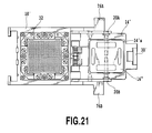
- FIG. 21 is a plan view showing a modification of a pressing member in the example illustrated in FIG. 18 ;
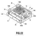
- FIG. 22 is a perspective view showing an appearance of a semiconductor device socket according to a fourth embodiment of the present invention.
- FIG. 23 is a plan view of the example illustrated in FIG. 22 ;
- FIG. 24 is a plan view showing a state where the inside of the socket body in the example illustrated in FIG. 22 is exposed;
- FIGS. 25A to 25D are views made available for explaining operations in the example illustrated in FIG. 22 ;
- FIG. 26 is a plan view showing an appearance of a semiconductor device socket according to a fifth embodiment of the present invention.
- FIG. 27 is a side view of the example shown in FIG. 26 ;
- FIGS. 28A and 28B are views made available for explaining operations in the example illustrated in FIG. 26 ;
- FIG. 29 is a plan view showing an appearance of a semiconductor device socket according to a sixth embodiment of the present invention.
- FIG. 30 is a side view of the example illustrated in FIG. 29 ;
- FIG. 31 is another side view made available for explaining an operation in the example illustrated in FIG. 29 ;
- FIG. 32 is a plan view made available for explaining the operation in the example illustrated in FIG. 29 ;
- FIG. 33 is a side view showing a state illustrated in FIG. 32 , including a partial cross-sectional view thereof;
- FIG. 34 is a side view showing another example of a lever member used in the example illustrated in FIG. 29 , including a partial cross-sectional view thereof;
- FIGS. 35A and 35B are views schematically showing still another example of the lever member used in the example illustrated in FIG. 29 ;
- FIGS. 36A and 36B are views schematically showing yet another example of the lever member used in the example illustrated in FIG. 29 .
- FIG. 2 shows an appearance of a semiconductor device socket according to a first embodiment of the present invention. It is to be noted that a single semiconductor device socket out of multiple semiconductor device sockets to be arranged on a printed circuit board PB (see FIG. 3 ) serving as a test board is representatively illustrated in FIG. 2 .
- PB printed circuit board
- the semiconductor device socket includes: a socket body 10 having, at its center, a housing section 10 A for housing a contact pin module and a positioning member 32 serving as a semiconductor device mounting section as described later; a pressing member support body 14 having one end rotational movably supported by the socket body 10 and being configured to support a pressing member to be described later so as to be movable inward; an operating lever member 12 having one end rotational movably supported by the socket body 10 and being configured to operate lever members 20 A and 20 B that are rotational movably supported by the pressing member support body 14 ; and a lock-unlock mechanism configured to lock or unlock the pressing member support body 14 and the operating lever member 12 to the socket body 10 .
- FIG. 2 shows a state where the pressing member support body 14 and the operating lever member 12 are locked with respect to the socket body 10 .
- a semiconductor device DV to be detachably placed on the positioning member 32 of the socket body 10 is formed as a substantially square-shaped semiconductor device of a ball grid array (BGA) type, which includes an electrode surface on which multiple ball-shaped electrode sections DVb (see FIG. 13C ) are formed in a matrix fashion.
- BGA ball grid array
- base end portions of the pressing member support body 14 and of the operating lever member 12 are rotational movably supported on one of short sides of the socket body 10 by use of a support shaft 26 .
- the support shaft 26 penetrates into one end side on the periphery of the housing section 10 A in the center.
- a base end section of a latch member 10 LN constituting part of the lock-unlock mechanism to be described later is rotational movably supported on the other short side of the socket body 10 by use of a support shaft 10 S.
- the support shaft 10 S penetrates into the other end side on the periphery of the housing section 10 A in the center.
- the contact pin module and the positioning member 32 are arranged inside the housing section 10 A.
- the positioning member 32 is supported so as to be vertically movable with respect to a substrate 38 to be described later, and includes, at its center, a semiconductor device housing section 32 A. Multiple pores are formed in a matrix fashion at a bottom of the semiconductor device housing section 32 A so as to correspond to layouts of the electrode sections of the semiconductor device DV and contact pins 42 ai .
- the electrode sections of the semiconductor device DV are arranged at the respective pores at the time of fitting of the semiconductor device DV.
- the positioning member 32 is provided with multiple holes into which guide pins are inserted in predetermined positions.
- One end of each guide pin 34 is fixed to the substrate 38 .
- coil springs 36 for biasing the positioning member 32 in a direction away from the substrate 38 are provided in multiple positions between the positioning member 32 and the substrate 38 . Accordingly, the positioning member 32 is guided by the guide pins 34 , and the electrode sections of the semiconductor device DV to be placed on the semiconductor device housing section 32 A touch on contact sections of the contact pins 42 ai through the above-described pores when the positioning member 32 is pressed toward the substrate 38 against biasing forces of the coil springs 36 . On the other hand, when the above-described pressing force is released, the positioning member 32 is biased to the remotest position from the substrate 38 by the biasing forces of the coil springs 36 as shown in FIG. 7 .
- positioning protrusions 32 P that allow four corners of a package of the semiconductor device to be detachably engaged therewith. In this way, relative positions of the contact pins 42 ai of the electrode sections of the semiconductor device, which is engaged with the positioning protrusions 32 P, are determined with respect to the contact sections.
- Each contact pin 42 ai is supported by inserting both ends thereof into pores which are formed on the substrate 40 and the substrate 38 , and includes a pair of contact terminals that is movably arranged on open ends on both ends of a metal sleeve, and a coil spring arranged between the contact terminals inside the sleeve and configured to bias the pair of contact terminals in a direction away from each other, for example.
- the operating lever member 12 includes arm sections that extend along side walls constituting long edge sides at an outer shell section of the housing section 10 A of the socket body 10 , a connecting portion configured to connect ends of the arm sections opposed to each other, and an engaging pin 18 arranged across other ends of the arm sections. Holes into which both ends of the support shaft 26 are inserted are formed on the other ends of the arm sections of the operating lever member 12 in positions adjacent to the engaging pin 18 . As shown in FIG. 6 , the support shaft 26 penetrates into a through hole at an end of the socket body 10 , the base end section of the pressing member support body 14 , and the above-described holes on the operating lever member 12 . In this way, the operating lever member 12 and the pressing member support body 14 are rotational movably supported. Engaging ends formed on ends of lever members 20 A and 20 B to be described later are slidably engaged with the engaging pin 18 .
- a distance Lb along the arm section from a region PA of the arm section of the operating lever member 12 which is a point of application of an operating force to the support shaft 26 is set longer than a mutual distance La between the engaging pin 18 and the support shaft 26 .
- the engaging ends on the ends of the lever members 20 A and 20 B to be described later are rendered easily swingable around supporting pins 24 A and 24 B as shown in FIG. 2 upon application of a relatively small operating force to the regions PA on the arm sections of the operating lever member 12 .
- a hook member 30 including a pair of lug sections 30 Na formed at a predetermined interval on one end of the hook member 30 is rotational movably arranged on the connecting portion at the arm sections of the operating lever member 12 .
- a coil spring (not shown) configured to bias the lug sections 30 Na of the hook member 30 in a direction to be engaged with a pair of lug sections (see FIG. 6 ) on the socket body 10 is arranged between the other end of the hook member 30 and a concave portion of the connecting portion.
- torsion coil springs 28 are wound around two positions at portions of the support shaft 26 exposed at the base end section of the pressing member support body 14 .
- the torsion coil springs 28 are configured to bias the pressing member support body 14 in a direction away from the pressing member support body 14 . Accordingly, when the latch member 10 LN constituting part of the lock-unlock mechanism is in an unlocked state, the operating lever member 12 and the pressing member support body 14 are biased to predetermined standby positions by the biasing forces of the torsion coil springs 28 as shown in FIGS. 4 and 5 .
- the pressing member support body 14 includes, at its center, an opening 14 a which is configured to movably house a pressing member 16 .
- the pressing member 16 includes a pressing surface formed at a lower end section thereof which is configured to press a surface of the semiconductor device.
- a pair of leg sections 16 F of the pressing member 16 which is guided to an inner peripheral surface of the opening 14 a , are connected to the lever members 20 A and 20 B respectively through slots 14 b by use of connecting pins 22 A and 22 B.
- the pressing member 16 includes, at its center, an opening 16 H which is configured to attach an unillustrated heat sink.
- Each of the slots 14 b of the pressing member support body 14 extends almost vertically with respect to an upper end surface and a lower end surface of the pressing member support body 14 .
- the pressing member 16 is biased in a direction to approach the pressing member support body 14 , i.e. in a direction to cause the pressing surface thereof to be away from the socket body 10 , by way of coil springs (not shown) respectively wound around machine screws Bs that are provided in four positions on the periphery of the opening 14 a .
- the pressing member 16 is allowed to move along the slots 14 b in conjunction with movements of the lever members 20 A and 20 B. Accordingly, the pressing surface of the pressing member 16 is allowed to move substantially in parallel to the upper end surface and the lower end surface of the pressing member support body 14 without causing an undesirable tilt.
- the lever members 20 A and 20 B are rotational movably supported by the pressing member support body 14 by way of supporting pins 24 A and 24 B which are respectively inserted into holes provided in intermediate parts of the lever members 20 A and 20 B.
- a mutual distance between the connecting pin 22 A and the supporting pin 24 A is set shorter than a distance between a central axis line of the supporting pin 24 A and an engaging end on one end of the lever member 20 A.
- a mutual distance between the connecting pin 22 B and the supporting pin 24 B is set shorter than a distance between a central axis line of the supporting pin 24 B and an engaging end on one end of the lever member 20 B.
- a pair of lug sections 14 Nb is formed with a predetermined interval at a tip end close to the above-described latch member 10 LN of the pressing member support body 14 .
- the pair of lug sections 14 Nb is respectively engaged with a pair of lug sections 10 Nb provided on the latch member 10 LN.
- the lock-unlock mechanism includes the latch member 10 LN made of metal, the pair of lug sections 14 Nb on the pressing member support body 14 , and the above-described hook member 30 of the operating lever member 12 .
- the latch member 10 N includes the lug sections 10 Nb which are formed along the short side of the socket body 10 with the predetermined interval. Moreover, as shown in FIG. 6 , in positions of the latch member 10 LN corresponding to a space between lug sections 10 nc on the socket body 10 , there are integrally formed protrusions 10 Na which are configured to kick up peripheral parts of the lug sections 30 Na of the hook member 30 so as to be disengaged from the lug sections 10 nc when the latch member 10 LN is rotated counterclockwise to be in the unlocked state, as indicated by a chain double-dashed line in FIG. 5 .
- the latch member 10 LN is rotated counterclockwise to the standby position.
- the protrusions 10 Na on the latch member 10 LN kick up the peripheral parts of the lug sections 30 Na of the hook member 30 so as to be disengaged from the lug sections 10 nc .
- the operating lever member 12 and the pressing member support body 14 are rotated back to initial positions almost simultaneously as shown in FIG. 4 by way of an elastic force of the torsion coil springs 28 .
- the semiconductor device DV is firstly fitted into the semiconductor device housing section 32 A of the positioning member 32 , and then the pressing member support body 14 is locked with respect to the socket body 10 as shown in FIG. 1 .
- a predetermined clearance is defined between the pressing surface of the pressing member 16 and an upper surface of a package of the semiconductor device DV.
- the pressing surface of the pressing member 16 and the upper surface of the package of the semiconductor device DV are set substantially parallel to each other.
- the operating force required to turn the latch member 10 LN into the locked state is relatively small because it is only necessary to rotate the pressing member support body 14 against the biasing forces of the torsion coil springs 28 .
- the operating lever member 12 is rotated around the support shaft 26 toward the pressing member support body 14 which is set to the locked state.
- the engaging pin 18 is rotated around the support shaft 26 .
- the engaging ends on the ends of the lever members 20 A and 20 B are respectively rotated upward around the supporting pins 24 A and 24 B.
- the pressing surface of the pressing member 16 is moved down against the biasing forces of the coil springs and touches on and presses the upper surface of the package of the semiconductor device at a predetermined pressure.
- the pressing surface of the pressing member touches on the upper surface of the package of the semiconductor device substantially in parallel thereto. Accordingly, the uniform pressure is applied to the upper surface of the package of the semiconductor device.
- the latch member 10 LN is rotated counterclockwise to the standby position as described previously.
- the protrusions 10 Na on the latch member 10 LN kick up the peripheral parts of the lug sections 30 Na of the hook member 30 so as to be disengaged from the lug sections 10 nc .
- the operating lever member 12 and the pressing member support body 14 are rotated almost simultaneously back to the initial positions as shown in FIGS. 4 and 5 by way of the elastic force of the torsion coil springs 28 . Thereafter, the semiconductor device DV can be taken out of the positioning member 32 of the socket body 10 .
- FIG. 8 shows an enlarged view of another example of one of contact pins used in the above-described contact pin module.
- FIGS. 13A to 13C the same constituents as those appearing in FIG. 7 will be designated by the same reference numerals and duplicate explanation will be omitted.
- the sleeve 58 is formed into a cylindrical shape by press work using a thin plate metal material such as a phosphor bronze material. Accordingly, the sleeve 58 includes a seam 58 Bu along a center axis line thereof. As enlarged and shown in FIG. 9 , four tapered contact sections 58 n are formed at one end of the sleeve 58 on a common circumference at intervals of about 90 degrees. In addition, as enlarged and shown in FIG. 11 , spring receivers 58 f are formed in four positions on the other end of the sleeve 58 so as to receive an end of the coil spring 56 . As shown in FIGS.
- protrusions 58 t for tentatively catching the coil spring are integrally formed in spaces between the two pairs of the spring receivers 58 f so as to protrude by a predetermined length along the center axis line of the sleeve 58 .
- a single nib 58 D is formed in a predetermined position close to the protrusions 58 t and the spring receivers 58 f .
- the nib 58 D formed substantially in a circular shape is configured to prevent a large-diameter section 54 D of the plunger 54 that is inserted into the sleeve 58 from falling off the sleeve 58 .
- the plunger 54 includes, at its one end, the large-diameter section 54 D configured to be inserted into the sleeve 58 , and, at its other end, a tapered contact section 54 c .
- a flange section 54 F is integrally formed in a position away from the contact section 54 c by a predetermined distance. As shown in FIG. 8 , one of surfaces of the flange section 54 F catches the other end of the coil spring 56 .
- the other surface of the flange section 54 F selectively touches on a surface on the periphery of a hole 40 a on the substrate 40 .
- the spring receivers 58 f of the sleeves 58 and the flange sections 54 F of the plungers 54 of the contact pins 52 ai incorporated between the substrate 40 and the substrate 38 in the contact pin module respectively touch on inner surface of the substrate 38 and the substrate 40 as shown in FIG. 13A by way of the biasing forces of the coil springs 58 before the contact pin module is mounted on the printed circuit board PB.
- the contact pin module is mounted on the printed circuit board PB as shown in FIG.
- the large-diameter sections 54 D of the plungers 54 are pulled into the sleeves 58 as the contact sections 54 c are pressed on the printed circuit board PB whereby the flange sections 54 F of the plungers 54 are separated from the inner surface on the periphery of the holes 40 a on the substrate 40 .
- the contact sections 58 n of the sleeves 58 touch on the electrode sections DVb of the semiconductor device DV and then the contact sections 58 n of the sleeves 58 are pressed against the biasing forces of the coil springs 56 .
- the nib 58 D substantially in the circular shape is formed on each of the sleeves 58 .
- the present invention is not limited only to this configuration.
- the above-described contact sections 58 n of the sleeve 58 are formed in four positions on the circumference having a predetermined diameter at intervals of about 90 degrees.
- a predetermined diameter is not limited only to this configuration.
- the sleeve 60 has a butt portion 60 Bu along a center axis line thereof.
- FIG. 17 shows an appearance of a semiconductor socket according to a second embodiment of the present invention.
- the same constituents as those in the example shown in FIG. 2 will be designated by the same reference numerals and duplicate explanation will be omitted.
- the operating lever member 12 includes the engaging pin 18 with which the engaging ends on the ends of the lever members 20 A and 20 B are slidably engaged.
- an operating lever member 12 ′ does not include the engaging pin 18 but includes a pair of cam sections 12 ′CA with which the respective engaging ends on the ends of the lever members 20 A and 20 B are slidably engaged.
- the cam sections 12 ′CA are respectively provided inside a base end section of the operating lever member 12 ′.
- Each of the cam sections 12 ′CA includes a cam surface configured to kick up the engaging end on the end of the lever member 20 A or 20 B to the highest position in a locked state of the operating lever member 12 ′ as shown in FIG. 17 and to lift down the engaging end on the end of the lever member 20 A or 20 B to the lowest position in an unlocked state of the operating lever member 12 ′.
- FIG. 18 shows an appearance of a semiconductor device socket according to a third embodiment of the present invention.
- FIGS. 18 to 20 the same constituents as those appearing in the example shown in FIG. 6 will be designated by the same reference numerals and duplicate explanation will be omitted.
- the semiconductor device socket includes: a socket body 10 ′ having, at its center, a positioning member 32 serving as a semiconductor device mounting section and a housing section 10 ′A for housing a contact pin module; a pressing member support body 14 ′ having one end rotational movably supported by the socket body 10 ′ and being configured to support a pressing member 16 ′ to be described later so as to be movable inward; operating lever members 76 A and 76 B each having one end rotational movably supported by the socket body 10 ′ and being configured to operate lever members 20 A and 20 B that are rotational movably supported by the pressing member support body 14 ′; and a lock-unlock mechanism configured to lock or unlock the pressing member support body 14 ′ to or from the socket body 10 ′.
- FIG. 20 shows a state where the pressing member support body 14 ′ is locked with respect to the socket body 10 ′.
- base end portions of the pressing member support body 14 ′ and of the operating lever members 76 A and 76 B are rotational movably supported on one of short sides of the socket body 10 ′ by use of a support shaft 26 that penetrates into one end side on the periphery of the housing section 10 ′A in the center.
- the contact pin module and the positioning member 32 are arranged inside the housing section 10 ′A.
- Each of the operating lever members 76 A and 76 B includes an arm section that extends along a side wall constituting a long edge side at an outer shell section of the housing section 10 ′A of the socket body 10 ′, and a cam section 76 CA to be formed at a base end section of the arm section. Holes into which both ends of the support shaft 26 penetrates are formed on the other ends of the arm sections of the operating lever members 76 A and 76 B. The support shaft 26 penetrates into a through hole at an end of the socket body 10 ′, the base end section of the pressing member support body 14 ′, and the above-described holes on the operating lever members 76 A and 76 B.
- the operating lever members 76 A and 76 B as well as the pressing member support body 14 ′ are rotational movably supported.
- Engaging ends formed on ends of the lever members 20 A and 20 B are slidably engaged with the cam sections 76 CA.
- the engaging ends on the ends of the lever members 20 A and 20 B are rendered easily swingable around supporting pins 24 A and 24 B as an operating force is applied to the arm sections of the operating lever members 76 A and 76 B.
- torsion coil springs 28 are wound around two positions at portions of the support shaft 26 exposed at the base end section of the pressing member support body 14 ′.
- the torsion coil springs 28 are configured to bias the pressing member support body 14 ′ in a direction away from the socket body 10 ′. Accordingly, when a hook member 30 ′ constituting part of the lock-unlock mechanism is in an unlocked state, the pressing member support body 14 ′ is biased to a predetermined standby position by the biasing forces of the torsion coil springs 28 .
- the pressing member support body 14 ′ includes, at its center, an opening 14 ′ a which is configured to movably house a pressing member 16 ′ therein.
- the pressing member 16 ′ includes a pressing surface formed at a lower end section thereof which is configured to press a surface of the semiconductor device.
- An outer peripheral surface of the pressing member 16 ′ to be guided to an inner peripheral surface of the opening 14 ′ a is connected to the lever members 20 A and 20 B respectively through slots 14 ′ b by use of connecting pins 22 A and 22 B.
- the pressing member 16 ′ includes, at its center, an opening 16 ′H which is configured to attach an unillustrated heat sink.
- Each of the slots 14 ′ b of the pressing member support body 14 ′ extends almost vertically with respect to an upper end surface and a lower end surface of the pressing member support body 14 ′.
- the pressing member 16 ′ is biased in a direction to approach the pressing member support body 14 ′, i.e. in a direction to cause the pressing surface thereof to be away from the socket body 10 ′, by way of coil springs 74 respectively wound around machine screws 72 that are provided in four positions at a portion constituting a bottom section of the opening 14 ′ a .
- the pressing member 16 ′ is allowed to move along the slots 14 ′ b in conjunction with movements of the lever members 20 A and 20 B. Accordingly, the pressing surface of the pressing member 16 ′ is allowed to move substantially in parallel to the upper end surface and the lower end surface of the pressing member support body 14 ′ without causing an undesirable tilt.
- the hook member 30 ′ including a pair of lug sections to be respectively engaged with a pair of lug sections 10 ′Nb is rotational movably provided at a tip end close to the lug sections 10 ′Nb of the socket body 10 ′.
- the lug sections of the hook member 30 ′ are biased in a direction to be respectively engaged with the pair of lug sections 10 ′Nb by use of coil springs.
- the lock-unlock mechanism includes the pair of lug sections 10 ′Nb of the socket body 10 ′, and the above-described hook member 30 ′ of the pressing member support body 14 ′.
- the semiconductor device DV is firstly fitted into a semiconductor device housing section 32 A of the positioning member 32 , and then the pressing member support body 14 ′ is locked with respect to the socket body 10 ′ as shown in FIG. 20 .
- a predetermined clearance is defined between the pressing surface of the pressing member 16 ′ and the upper surface of the package of the semiconductor device DV.
- the pressing surface of the pressing member 16 ′ and the upper surface of the package of the semiconductor device DV are set substantially parallel to each other.
- the operating force required herein is relatively small because it is only necessary to rotate the pressing member support body 14 ′ against the biasing forces of the torsion coil springs 28 .
- the operating lever members 76 A and 76 B are rotated around the support shaft 26 .
- the engaging ends on the ends of the lever members 20 A and 20 B are respectively rotated upward around the supporting pins 24 A and 24 B.
- the pressing surface of the pressing member 16 ′ is moved down against the biasing forces of the coil springs and touches on and presses the upper surface of the package of the semiconductor device at a predetermined pressure.
- the pressing surface of the pressing member 16 ′ touches on the upper surface of the package of the semiconductor device substantially in parallel thereto. Accordingly, the uniform pressure is applied to the upper surface of the package of the semiconductor device.
- the lug sections of the hook member 30 ′ are disengaged from the lug sections 10 ′Nb of the socket body 10 ′, whereby the pressing member support body 14 ′ is rotated back to the initial position by way of the resilience of the torsion coil springs 28 . Thereafter, the semiconductor device DV can be taken out of the positioning member 32 of the socket body 10 ′.
- the pressing member 16 ′ includes an opening 16 ′H for attaching the heat sink which is provided at the central part thereof.
- the present invention is not limited only to this configuration.
- the pressing member 16 ′′ does not have to include the aforementioned fitting opening.
- FIG. 21 the same constituents as those appearing in the example shown in FIG. 18 will be designated by the same reference numerals and duplication explanation will be omitted.
- FIG. 22 shows an appearance of a semiconductor device socket according to a fourth embodiment of the present invention.
- FIGS. 22 to 25D the same constituents as those appearing in the example shown in FIG. 18 will be designated by the same reference numerals and duplicate explanation will be omitted.
- the semiconductor device socket includes: a socket body 11 having, at its center, a positioning member 32 serving as a semiconductor device mounting section and a housing section 11 A for housing a contact pin module; a pressing member support body 14 ′ having one end rotational movably supported by the socket body 11 and being configured to support a pressing member to be described later so as to be movable inward; an operating lever member 82 having one end rotational movably supported by the socket body 11 and being configured to operate lever members 20 A and 20 B that are rotational movably supported by the pressing member support body 14 ′; and a lock-unlock mechanism configured to lock or unlock the pressing member support body 14 ′ and the operating lever member 82 to or from the socket body 11 .
- FIG. 22 shows a state where the pressing member support body 14 ′ and the operating lever member 82 are locked with respect to the socket body 11 .
- Base end portions of the pressing member support body 14 ′ and of the operating lever member 82 are rotational movably supported on one of short sides of the socket body 11 by use of a support shaft 26 that penetrates into one end side on the periphery of the housing section 11 A in the center.
- a base end section of a latch member 70 constituting part of the lock-unlock mechanism to be described later is rotational movably supported on the other short side of the socket body 11 by use of a support shaft 11 S that penetrates into the other end side on the periphery of the housing section 11 A in the center.
- the contact pin module and the positioning member 32 are arranged inside the housing section 11 A.
- the operating lever member 82 includes arm sections that extend along side walls constituting long edge sides at an outer shell section of the housing section 11 A of the socket body 11 , and a connecting portion configured to connect ends of the arm sections opposed to each other. Holes into which both ends of the support shaft 26 penetrate are formed on the other ends of the arm sections of the operating lever member 82 . As shown in FIG. 6 , the support shaft 26 penetrates into a through hole at an end of the socket body 11 , the base end section of the pressing member support body 14 ′, and the above-described holes on the operating lever member 82 . In this way, the operating lever member 82 and the pressing member support body 14 ′ are rotational movably supported.
- Cam sections 82 CA are formed on the periphery of the holes into which the support shaft 26 penetrates inside the arm sections of the operating lever member 82 .
- the engaging ends on the ends of the lever members 20 A and 20 B to be described later are slidably engaged with the cam sections 82 CA.
- a distance along the arm section from a region of the arm section of the operating lever member 82 which is a point of application of an operating force to the support shaft 26 is set longer than a distance from a center axis line of the supports shaft 26 to a cam surface of the cam section 82 CA.
- the engaging ends on the ends of the lever members 20 A and 20 B are rendered easily swingable around supporting pins 24 A and 24 B upon application of a relatively small operating force to the arm sections of the operating lever member 82 .
- the distance along the arm section from the region of the arm section of the operating lever member 82 being the point of application of the operating force to the support shaft 26 is set longer than a length L 2 of the arm sections of the operating lever members 76 A and 76 B. Accordingly, the operating force is further reduced as compared to the case of using the operating lever members 76 A and 76 B.
- lug sections 82 N with which lug sections of the latch member 70 are selectively engaged are formed at a predetermined interval on the connecting portion of the operating lever member 82 .
- a hook member 30 ′ including a pair of lug sections formed at a predetermined interval on one end thereof is rotational movably provided at a tip end of the pressing member support body 14 ′.
- a coil spring (not shown) configured to bias the lug sections of the hook member 30 ′ in a direction to be engaged with a pair of lug sections 11 Nb (see FIG. 24 ) on the socket body 11 is arranged between the other end of the hook member 30 ′ and a concave portion of the pressing member support body 14 ′.
- torsion coil springs 28 are wound around two positions at portions of the support shaft 26 exposed at the base end section of the pressing member support body 14 ′. Accordingly, when the hook member 30 ′ constituting part of the lock-unlock mechanism is in an unlocked state, the pressing member support body 14 ′ is biased to a predetermined standby position by the biasing forces of the torsion coil springs 28 as shown in FIG. 25A .
- the pressing member 16 ′ includes, at its center, an opening 16 ′H which is configured to attach a heat sink.
- a heat transfer surface section of a heat sink 80 configured to touch on a surface of a package of a semiconductor device DV for radiation is exposed on an inner surface side of the pressing member 16 ′.
- the heat sink 80 is fixed to an outer surface of the pressing member 16 ′.
- the lock-unlock mechanism includes the latch member 70 made of metal, the lug sections 82 N of the operating lever member 82 , the hook member 30 ′ of the pressing member support body 14 ′, and the lug sections 11 Nb of the socket body 11 .
- the latch member 70 includes lug sections 70 Nb which are rotational movably supported on the socket body 11 by using the support shaft 11 S and formed along a short side of the socket body 11 with a predetermined interval. Convex sections on the connecting portion of the operating lever member 82 are inserted into the lug sections 70 Nb when the operating lever member 82 is locked with respect to the socket body 11 . Moreover, the latch member 70 is biased in a direction to be engaged with the lug sections 82 N of the operating lever member 82 by use of a torsion coil spring.
- the latch member 70 is rotated counterclockwise while the hook member 30 ′ is rotated clockwise. In this way, the pressing member support body 14 ′ is rotated back to the initial position by way of the resilience of the torsion coil springs 28 .
- the semiconductor device DV is firstly fitted into the semiconductor device housing section 32 A of the positioning member 32 in a state shown in FIG. 25A , and then the pressing member support body 14 ′ is locked with respect to the socket body 11 as shown in FIG. 25C .
- a predetermined clearance CL is defined between the pressing surface of the pressing member 16 ′ and an upper surface of a package of the semiconductor device DV.
- the pressing surface of the pressing member 16 ′ and the upper surface of the package of the semiconductor device DV are set substantially parallel to each other.
- the operating force required to be applied to the pressing member support body 14 ′ to turn the hook member 30 ′ into the locked state is relatively small because it is only necessary to rotate the pressing member support body 14 ′ against the biasing forces of the torsion coil springs 28 .
- the operating lever member 82 is rotated around the support shaft 26 toward the pressing member support body 14 ′ which is set to the locked state.
- the cam surfaces of the cam sections 82 CA are rotated around the support shaft 26 .
- the engaging ends on the ends of the lever members 20 A and 20 B are respectively rotated upward around the supporting pins 24 A and 24 B.
- the pressing surface of the pressing member 16 ′ is moved down against the biasing forces of the coil springs and touches on and presses the upper surface of the package of the semiconductor device at a predetermined pressure.
- the pressing surface of the pressing member 16 ′ touches on the upper surface of the package of the semiconductor device substantially in parallel thereto. Accordingly, the uniform pressure is applied to the upper surface of the package of the semiconductor device.
- the latch member 70 is rotated counterclockwise while the hook member 30 ′ is rotated clockwise as described previously. In this way, the pressing member support body 14 ′ is rotated back to the initial position by way of the resilience of the torsion coil springs 28 . Thereafter, the semiconductor device DV can be taken out of the positioning member 32 of the socket body 11 .
- FIG. 26 shows an appearance of a semiconductor device socket according to a fifth embodiment of the present invention.
- the operating lever members 76 A and 76 B are rotational movably supported by the socket body 10 ′.
- respective operating lever members 92 A and 92 B are rotational movably supported by support tables 90 A and 90 B which are disposed on a printed circuit board PB.
- FIGS. 27 , 28 A, and 28 B the same constituents as those appearing in the example shown in FIG. 18 will be designated by the same reference numerals and duplicate explanation will be omitted.
- Each of the support tables 90 A and 90 B is disposed to face a support shaft 26 in such a manner that each of center axis lines of the support tables 90 A and 90 B are located on a center axis line common to a center axis line of the support shaft 26 on the socket body 10 ′.
- Ends of the operating members 92 A and 92 B are connected to each other by using an engaging pin 94 .
- other ends of the operating members 92 A and 92 B are rotational movably supported by the support tables 90 A and 90 B, respectively.
- the semiconductor device DV in order to fit a semiconductor device DV onto a positioning member 32 of the socket body 10 ′, the semiconductor device DV is firstly fitted into a semiconductor device housing section 32 A of the positioning member 32 in a state shown in FIG. 27 , and then a pressing member support body 14 ′ is locked with respect to the socket body 10 ′.
- a predetermined clearance is defined between a pressing surface of a pressing member 16 ′ and an upper surface of a package of the semiconductor device DV.
- the pressing surface of the pressing member 16 ′ and the upper surface of the package of the semiconductor device DV are set substantially parallel to each other.
- an operating force required to be applied to the pressing member support body 14 ′ is relatively small because it is only necessary to rotate the pressing member support body 14 ′ against biasing forces of torsion coil springs 28 .
- the operating lever members 92 A and 92 B are rotated from a state of being substantially parallel to a surface of a printed circuit board PB as shown in FIG. 28A , to a state of being substantially perpendicular to the surface of the printed circuit board PB as shown in FIG. 28B .
- the engaging pin 94 is rotated so as to slide on engaging ends on ends of lever members 20 A and 20 B. Accordingly, the engaging ends on the ends of the lever members 20 A and 20 B are respectively rotated upward around supporting pins 24 A and 24 B.
- the pressing surface of the pressing member 16 ′ is moved down against biasing forces of coil springs and touches on and presses the upper surface of the package of the semiconductor device at a predetermined pressure.
- the pressing surface of the pressing member touches on the upper surface of the package of the semiconductor device substantially in parallel thereto. Accordingly, the uniform pressure is applied to the upper surface of the package of the semiconductor device.
- lug sections of a hook member 30 ′ are disengaged from lug sections 10 ′Nb of the socket body 10 ′.
- the operating lever members 92 A and 92 B are rotated backed to the initial state as shown in FIG. 28A .
- the pressing member support body 14 ′ is rotated by way of the resilience of the torsion coil springs 28 . Thereafter, the semiconductor device DV can be taken out of the positioning member 32 of the socket body 10 ′.
- FIG. 29 shows an appearance of a semiconductor device socket according to a sixth embodiment of the present invention.
- the pressing surface of the pressing member 16 is moved down against the biasing forces of the coil springs as the ends of the lever members 20 A and 20 B are rotated upward due to rotation of the engaging pin 18 around the support shaft 26 .
- a pressing surface of a pressing member 46 is moved down against biasing forces of coil springs as ends of lever members 50 A and 50 B are rotated downward due to rotation of an engaging pin 62 PA around a support shaft 26 .
- FIGS. 29 to 33 the same constituents as those appearing in the example shown in FIG. 6 will be designated by the same reference numerals and duplicate explanation will be omitted.
- the semiconductor device socket comprises: a socket body 10 having, at its center, a housing section 10 A for housing a positioning member 32 and a contact pin module; a pressing member support body 44 having one end rotational movably supported by the socket body 10 and being configured to support a pressing member to be described later so as to be movable inward; an operating lever member 62 having one end rotational movably supported by the socket body 10 and being configured to operate lever members 50 A and 50 B that are rotational movably supported by the pressing member support body 44 ; and a lock-unlock mechanism configured to lock or unlock the pressing member support body 44 and the operating lever member 62 to the socket body 10 .
- FIGS. 32 and 33 show a state where the pressing member support body 44 and the operating lever member 62 are locked with respect to the socket body 10 .
- base end portions of the pressing member support body 44 and of the operating lever member 62 are rotational movably supported on one of short sides of the socket body 10 by use of the support shaft 26 .
- the support shaft 26 penetrates into one end side of the periphery of the housing section 10 A in the center.
- a base end section of a latch member 10 LN constituting part of the lock-unlock mechanism to be described later is rotational movably supported on the other short side of the socket body 10 by use of a support shaft 10 S.
- the support shaft 10 S penetrates into the other end side of the periphery of the housing section 10 A in the center.
- a distance Lb along the arm section from a region PA of the arm section of the operating lever member 62 which is a point of application of an operating force to the support shaft 26 is set longer than a mutual distance La between the engaging pin 62 PA and the support shaft 26 .
- the engaging ends on the ends of the lever members 50 A and 50 B to be described later are rendered easily swingable around supporting pins 24 A and 24 B upon application of a relatively small operating force to the regions PA on the arm sections of the operating lever member 62 .
- a hook member 30 having a pair of lug sections 30 Na formed at a predetermined interval on one end of the hook member 30 is rotational movably connected to the connecting portion at the arm sections of the operating lever member 62 .
- torsion coil springs 28 are wound around two positions at portions of the support shaft 26 exposed at the base end section of the pressing member support body 44 .
- the torsion coil springs 28 are configured to bias the pressing member support body 44 in a direction away from the socket body 10 . Accordingly, when the latch member 10 LN constituting part of the lock-unlock mechanism is in an unlocked state, the operating lever member 62 and the pressing member support body 44 are biased to predetermined standby positions by the biasing forces of the torsion coil springs 28 as shown in FIG. 30 .
- the pressing member support body 44 has, at its center, an opening 44 a which is configured to movably house a pressing member 46 therein.
- the pressing member 46 has a pressing surface formed at a lower end section thereof which is configured to press a surface of the semiconductor device.
- a pair of leg sections (not shown) of the pressing member 46 which is guided to an inner peripheral surface of the opening 44 a , are connected to the lever members 50 A and 50 B respectively through slots 44 b by use of connecting pins 22 A and 22 B.
- the pressing member 46 has, at its center, a attaching opening 46 H which is configured to attach an unillustrated heat sink.
- Each of the slots 44 b of the pressing member support body 44 extends almost vertically with respect to an upper end surface and a lower end surface of the pressing member support body 44 .
- the pressing member 46 is biased in a direction to approach the pressing member support body 44 , i.e. in a direction to cause the pressing surface thereof to be away from the socket body 10 , by way of coil springs (not shown) respectively wound around machine screws Bs that are provided in four positions on the periphery of the opening 44 a .
- the pressing member 46 is allowed to move along the slots 44 b in conjunction with movements of the lever members 50 A and 50 B. Accordingly, the pressing surface of the pressing member 46 is allowed to move substantially in parallel to the upper end surface and the lower end surface of the pressing member support body 44 without causing an undesirable tilt.
- the lever members 50 A and 50 B are rotational movably supported by the pressing member support body 44 by way of supporting pins 24 A and 24 B which are respectively inserted into holes provided ends thereof.
- a mutual distance between the connecting pin 22 A and the supporting pin 24 A is set shorter than a distance between a center axis line of the supporting pin 24 A and an engaging end on one end of the lever member 50 A.
- a mutual distance between the connecting pin 22 B and the supporting pin 24 B is set shorter than a distance between a center axis line of the supporting pin 24 B and an engaging end on one end of the lever member 50 B.
- a pair of lug sections 44 Nb is formed with a predetermined interval at a tip end close to the above-described latch member 10 LN of the pressing member support body 44 .
- the pair of lug sections 44 Nb is respectively engaged with a pair of lug sections 10 Nb provided on the latch member 10 LN.
- the lock-unlock mechanism comprises the latch member 10 LN made of metal, the pair of lug sections 44 Nb on the pressing member support body 44 , and the above-described hook member 30 of the operating lever member 62 .
- the latch member 10 LN is rotated counterclockwise to the standby position.
- protrusions 10 Na of the latch member 10 LN kick up peripheral parts of the lug sections 30 Na of the hook member 30 so as to be disengaged from the lug sections 10 nc .
- the operating lever member 62 and the pressing member support body 44 are rotated back to initial positions almost simultaneously as shown in FIG. 30 by way of the resilience of the torsion coil springs 28 .
- the operating force required to be applied to the pressing member support body 44 to turn the latch member 10 LN into the locked state is relatively small because it is only necessary to rotate the pressing member support body 44 against the biasing forces of the torsion coil springs 28 .
- the operating lever member 62 is rotated around the support shaft 26 toward the pressing member support body 44 which is set to the locked state.
- the engaging pins 62 PA are rotated around the support shaft 26 .
- the engaging ends on the ends of the lever members 50 A and 50 B are respectively rotated downward around the supporting pins 24 A and 24 B.
- the pressing surface of the pressing member 46 is moved down against the biasing forces of the coil springs and touches on the upper surface of the package of the semiconductor device and presses the upper surface at a predetermined pressure.
- the uniform pressure is applied to the upper surface of the package of the semiconductor device.
- the latch member 10 LN is rotated counterclockwise to the standby position as described previously.
- the protrusions 10 Na on the latch member 10 LN kick up the peripheral parts of the lug sections 30 Na of the hook member 30 so as to be disengaged from the lug sections 10 nc .
- the operating lever member 62 and the pressing member support body 44 are rotated almost simultaneously to return to the initial positions by way of the resilience of the torsion coil springs 28 . Thereafter, the semiconductor device DV can be taken out of the positioning member 32 of the socket body 10 .
- the mutual distance between the connecting pin 22 A and the supporting pin 24 A is set shorter than the distance between the center axis line of the supporting pin 24 A and the engaging end on one end of the lever member 50 A.
- the mutual distance between the connecting pin 22 B and the supporting pin 24 B is set shorter than the distance between the center axis line of the supporting pin 24 B and the engaging end on one end of the lever member 50 B.
- lever members 50 A and 50 B it may be provided with lever members 60 A and 60 B as shown in FIG. 34 , which have longer total lengths than total lengths of the lever members 50 A and 50 B, for example.
- a mutual distance between the connecting pin 22 A and the supporting pin 24 A in the lever members 60 A and 60 B is set shorter than the case of the lever members 50 A and 50 B.
- the distance from the supporting pins 24 A and 24 B to the engaging ends is set longer.
- the connecting pins 22 A and 22 B as well as the supporting pins 24 A and 24 B are configured to penetrate with predetermined clearances into circular holes formed on the lever members 50 A and 50 B.
- this example according to the present invention is not limited only to this configuration.
- the connecting pins 22 A and 22 B may penetrate with predetermined clearances into slots 66 b that extend in a longitudinal direction thereof. Slots 66 b are formed near the center position of each of the lever members 66 A and 66 B.
- Circular holes 66 a formed at one end of the lever members 66 A and 66 B, respectively are connected to an end of the supporting pins 24 A and 24 B with predetermined clearances.
- the pressing member 46 presses a semiconductor device as shown in FIG. 35B , the pressing member 46 is allowed to be moved up and down smoothly and to be guided by the slots 44 b with peripheral portions of the connecting pins 22 A and 22 B touching and sliding to the slots 66 b.
- the supporting pins 24 A and 24 B may penetrate with predetermined clearances into slots 68 a that extend in a longitudinal direction thereof.
- Slots 68 a are formed at one end of each of the lever members 68 A and 68 B.
- Circular holes 68 b formed near the center position of each of the lever members 68 A and 68 B, respectively are connected to an end of the connecting pins 22 A and 22 B with predetermined clearances.
- the pressing member 46 presses a semiconductor device as shown in FIG. 36B , the pressing member 46 is allowed to be moved up and down smoothly and to be guided by the slots 44 b with peripheral portions of the supporting pins 24 A and 24 B touching and sliding to the slots 68 a.
Abstract
Description
Claims (13)
Applications Claiming Priority (4)
| Application Number | Priority Date | Filing Date | Title |
|---|---|---|---|
| JP2008326237 | 2008-12-22 | ||
| JP2008-326237 | 2008-12-22 | ||
| JP2009-139389 | 2009-06-10 | ||
| JP2009139389A JP5196327B2 (en) | 2008-12-22 | 2009-06-10 | Socket for semiconductor device |
Publications (2)
| Publication Number | Publication Date |
|---|---|
| US20100159731A1 US20100159731A1 (en) | 2010-06-24 |
| US7815456B2 true US7815456B2 (en) | 2010-10-19 |
Family
ID=42266764
Family Applications (1)
| Application Number | Title | Priority Date | Filing Date |
|---|---|---|---|
| US12/502,901 Active US7815456B2 (en) | 2008-12-22 | 2009-07-14 | Semiconductor device socket |
Country Status (2)
| Country | Link |
|---|---|
| US (1) | US7815456B2 (en) |
| JP (1) | JP5196327B2 (en) |
Cited By (8)
| Publication number | Priority date | Publication date | Assignee | Title |
|---|---|---|---|---|
| US8147266B2 (en) * | 2007-07-27 | 2012-04-03 | Molex Incorporated | Fastener for a socket connector |
| US20120083169A1 (en) * | 2010-05-06 | 2012-04-05 | Heng Stephen F | Circuit board socket with support structure |
| US8837162B2 (en) | 2010-05-06 | 2014-09-16 | Advanced Micro Devices, Inc. | Circuit board socket with support structure |
| US9711899B2 (en) * | 2014-03-31 | 2017-07-18 | Enplas Corporation | Latch mechanism having latch locking parts to prevent rotation of latch parts |
| US20180190561A1 (en) * | 2016-12-29 | 2018-07-05 | Foxconn Interconnect Technology Limited | Easily detachable cpu clip |
| US10305218B2 (en) * | 2015-05-05 | 2019-05-28 | Harting Electric Gmbh & Co. Kg | Protective cap for an attachment housing |
| US20210378121A1 (en) * | 2020-06-02 | 2021-12-02 | Yamaichi Electronics Co., Ltd. | Connector, ic package, and method of mounting contacts to housing of connector |
| US11522327B2 (en) * | 2017-12-27 | 2022-12-06 | Enplas Corporation | Opening / closing mechanism of opening / closing body |
Families Citing this family (9)
| Publication number | Priority date | Publication date | Assignee | Title |
|---|---|---|---|---|
| JP6243130B2 (en) * | 2013-03-27 | 2017-12-06 | 株式会社エンプラス | Electrical contact and socket for electrical parts |
| JP6251104B2 (en) * | 2014-03-31 | 2017-12-20 | 株式会社エンプラス | Elevating mechanism and socket for electrical parts |
| JP2017050202A (en) * | 2015-09-03 | 2017-03-09 | 株式会社エンプラス | Socket for electric component |
| JP7018309B2 (en) * | 2017-12-27 | 2022-02-10 | 株式会社エンプラス | Socket for electrical components |
| KR101926387B1 (en) * | 2018-10-10 | 2018-12-10 | 황동원 | Socket device for testing an IC |
| KR102566041B1 (en) * | 2019-11-05 | 2023-08-16 | 주식회사 프로웰 | Semiconductor element test device |
| JP2021086807A (en) * | 2019-11-29 | 2021-06-03 | 株式会社エンプラス | Socket and inspection socket |
| JP2022112095A (en) * | 2021-01-21 | 2022-08-02 | 山一電機株式会社 | Heatsink unit, ic socket, method of manufacturing semiconductor package, and semiconductor package |
| KR102619575B1 (en) * | 2021-07-13 | 2023-12-29 | 주식회사 아이에스시 | Pusher apparatus for test |
Citations (35)
| Publication number | Priority date | Publication date | Assignee | Title |
|---|---|---|---|---|
| JPS59135699A (en) | 1983-01-21 | 1984-08-03 | Hitachi Ltd | Semiconductor storage device |
| US4515425A (en) | 1983-02-28 | 1985-05-07 | Yamaichi Electric Mfg. Co., Ltd. | IC socket with IC package pressing means |
| JPH0637349A (en) | 1992-05-18 | 1994-02-10 | General Electric Co <Ge> | Avalance photodiode doped with platinum |
| JPH0686293A (en) | 1992-09-07 | 1994-03-25 | Nec Corp | Image tracking device |
| JPH0719983A (en) | 1993-07-05 | 1995-01-20 | Akashi:Kk | Balance weight fitting device |
| JPH07120549A (en) | 1993-10-28 | 1995-05-12 | Fujitsu Ltd | Fm-cw radar |
| JPH0846335A (en) | 1994-07-26 | 1996-02-16 | Oki Electric Ind Co Ltd | Heat conduction sheet |
| US5518410A (en) | 1993-05-24 | 1996-05-21 | Enplas Corporation | Contact pin device for IC sockets |
| JPH1074571A (en) | 1997-05-09 | 1998-03-17 | Enplas Corp | Ic socket for bga type ic package |
| JPH10256764A (en) | 1997-03-17 | 1998-09-25 | Mitsubishi Electric Corp | Heat-dissipating material |
| JP2822850B2 (en) | 1993-07-19 | 1998-11-11 | 株式会社エンプラス | IC socket |
| JPH1126123A (en) | 1997-07-03 | 1999-01-29 | Enplas Corp | Socket for electric component |
| JPH1154670A (en) | 1997-08-01 | 1999-02-26 | Enplas Corp | Electric component socket |
| JPH11251026A (en) | 1998-02-27 | 1999-09-17 | Enplas Corp | Ic socket |
| JPH11251027A (en) | 1998-02-27 | 1999-09-17 | Enplas Corp | Ic socket |
| JP2000171507A (en) | 1998-12-04 | 2000-06-23 | Enplas Corp | Electric component contact unit and unit for inspecting electric component using the same |
| JP2000182739A (en) | 1998-12-18 | 2000-06-30 | Enplas Corp | Socket for electric parts |
| US6126467A (en) | 1998-07-22 | 2000-10-03 | Enplas Corporation | Socket for electrical parts |
| US6293809B1 (en) | 1998-12-28 | 2001-09-25 | Enplas Corporation | Socket for electrical parts |
| US6386896B2 (en) | 1998-12-25 | 2002-05-14 | Enplas Corporation | Socket for electrical parts |
| JP2002202729A (en) | 2001-10-22 | 2002-07-19 | Matsushita Electric Ind Co Ltd | Plasma display device |
| JP2003007942A (en) | 2001-06-21 | 2003-01-10 | Yamaichi Electronics Co Ltd | Fitting structure of heat sink |
| JP2003123926A (en) | 2001-10-11 | 2003-04-25 | Yamaichi Electronics Co Ltd | Ic socket |
| JP2004014873A (en) | 2002-06-07 | 2004-01-15 | Yamaichi Electronics Co Ltd | Socket for electronic component |
| JP2004047163A (en) | 2002-07-09 | 2004-02-12 | Enplas Corp | Socket for electrical component |
| JP2004227904A (en) | 2003-01-22 | 2004-08-12 | Enplas Corp | Socket for electrical component |
| US6776641B2 (en) * | 2002-04-09 | 2004-08-17 | Enplas Corporation | Socket for electrical parts |
| JP2004296155A (en) | 2003-03-26 | 2004-10-21 | Enplas Corp | Socket for electric component |
| JP2005061948A (en) | 2003-08-11 | 2005-03-10 | Enplas Corp | Socket for electric component |
| US6872083B2 (en) * | 2001-11-30 | 2005-03-29 | Enplas Corporation | Socket for electrical parts |
| US6966783B2 (en) | 2002-07-09 | 2005-11-22 | Enplas Corporation | Contact pin and socket for electrical parts provided with contact pin |
| US7230830B2 (en) * | 2004-04-16 | 2007-06-12 | Yamaichi Electronics Co., Ltd. | Semiconductor device socket |
| US7559784B2 (en) * | 2007-05-07 | 2009-07-14 | Hon Hai Precision Ind. Co., Ltd. | IC socket |
| US20090291582A1 (en) * | 2008-05-26 | 2009-11-26 | Hon Hai Precision Industry Co., Ltd. | Burn-in socket with hard stopper |
| US7666016B2 (en) * | 2004-05-14 | 2010-02-23 | 3M Innovative Properties Company | IC socket |
Family Cites Families (6)
| Publication number | Priority date | Publication date | Assignee | Title |
|---|---|---|---|---|
| JPH06168756A (en) * | 1992-11-30 | 1994-06-14 | Nec Kansai Ltd | Contact pin |
| JP3231690B2 (en) * | 1997-12-01 | 2001-11-26 | 株式会社ヨコオ | Socket for IC package |
| JP3619413B2 (en) * | 2000-01-18 | 2005-02-09 | 株式会社エンプラス | Socket for electrical parts |
| JP2003167001A (en) * | 2001-11-29 | 2003-06-13 | Yamaichi Electronics Co Ltd | Contact probe of socket for electronic parts and electronic parts using the same |
| JP4025323B2 (en) * | 2004-08-19 | 2007-12-19 | 山一電機株式会社 | Socket for semiconductor device |
| JP4857046B2 (en) * | 2006-08-02 | 2012-01-18 | 株式会社エンプラス | Electrical contact and socket for electrical parts |
-
2009
- 2009-06-10 JP JP2009139389A patent/JP5196327B2/en active Active
- 2009-07-14 US US12/502,901 patent/US7815456B2/en active Active
Patent Citations (39)
| Publication number | Priority date | Publication date | Assignee | Title |
|---|---|---|---|---|
| JPS59135699A (en) | 1983-01-21 | 1984-08-03 | Hitachi Ltd | Semiconductor storage device |
| US4515425A (en) | 1983-02-28 | 1985-05-07 | Yamaichi Electric Mfg. Co., Ltd. | IC socket with IC package pressing means |
| JPH0637349A (en) | 1992-05-18 | 1994-02-10 | General Electric Co <Ge> | Avalance photodiode doped with platinum |
| JPH0686293A (en) | 1992-09-07 | 1994-03-25 | Nec Corp | Image tracking device |
| US5518410A (en) | 1993-05-24 | 1996-05-21 | Enplas Corporation | Contact pin device for IC sockets |
| JPH0719983A (en) | 1993-07-05 | 1995-01-20 | Akashi:Kk | Balance weight fitting device |
| JP2822850B2 (en) | 1993-07-19 | 1998-11-11 | 株式会社エンプラス | IC socket |
| JPH07120549A (en) | 1993-10-28 | 1995-05-12 | Fujitsu Ltd | Fm-cw radar |
| JPH0846335A (en) | 1994-07-26 | 1996-02-16 | Oki Electric Ind Co Ltd | Heat conduction sheet |
| JPH10256764A (en) | 1997-03-17 | 1998-09-25 | Mitsubishi Electric Corp | Heat-dissipating material |
| JPH1074571A (en) | 1997-05-09 | 1998-03-17 | Enplas Corp | Ic socket for bga type ic package |
| JPH1126123A (en) | 1997-07-03 | 1999-01-29 | Enplas Corp | Socket for electric component |
| JPH1154670A (en) | 1997-08-01 | 1999-02-26 | Enplas Corp | Electric component socket |
| JPH11251026A (en) | 1998-02-27 | 1999-09-17 | Enplas Corp | Ic socket |
| JPH11251027A (en) | 1998-02-27 | 1999-09-17 | Enplas Corp | Ic socket |
| US6213806B1 (en) | 1998-02-27 | 2001-04-10 | Enplas Corporation | IC socket |
| US6155859A (en) | 1998-02-27 | 2000-12-05 | Enplas Corporation | IC socket having pressure cover and associated stopper |
| US6126467A (en) | 1998-07-22 | 2000-10-03 | Enplas Corporation | Socket for electrical parts |
| JP2000171507A (en) | 1998-12-04 | 2000-06-23 | Enplas Corp | Electric component contact unit and unit for inspecting electric component using the same |
| JP2000182741A (en) | 1998-12-18 | 2000-06-30 | Enplas Corp | Socket for electric parts |
| JP2000182739A (en) | 1998-12-18 | 2000-06-30 | Enplas Corp | Socket for electric parts |
| US6443741B1 (en) | 1998-12-18 | 2002-09-03 | Enplas Corporation | Socket for electrical parts |
| US6386896B2 (en) | 1998-12-25 | 2002-05-14 | Enplas Corporation | Socket for electrical parts |
| US6293809B1 (en) | 1998-12-28 | 2001-09-25 | Enplas Corporation | Socket for electrical parts |
| JP2003007942A (en) | 2001-06-21 | 2003-01-10 | Yamaichi Electronics Co Ltd | Fitting structure of heat sink |
| JP2003123926A (en) | 2001-10-11 | 2003-04-25 | Yamaichi Electronics Co Ltd | Ic socket |
| JP2002202729A (en) | 2001-10-22 | 2002-07-19 | Matsushita Electric Ind Co Ltd | Plasma display device |
| US6872083B2 (en) * | 2001-11-30 | 2005-03-29 | Enplas Corporation | Socket for electrical parts |
| US6776641B2 (en) * | 2002-04-09 | 2004-08-17 | Enplas Corporation | Socket for electrical parts |
| JP2004014873A (en) | 2002-06-07 | 2004-01-15 | Yamaichi Electronics Co Ltd | Socket for electronic component |
| JP2004047163A (en) | 2002-07-09 | 2004-02-12 | Enplas Corp | Socket for electrical component |
| US6966783B2 (en) | 2002-07-09 | 2005-11-22 | Enplas Corporation | Contact pin and socket for electrical parts provided with contact pin |
| JP2004227904A (en) | 2003-01-22 | 2004-08-12 | Enplas Corp | Socket for electrical component |
| JP2004296155A (en) | 2003-03-26 | 2004-10-21 | Enplas Corp | Socket for electric component |
| JP2005061948A (en) | 2003-08-11 | 2005-03-10 | Enplas Corp | Socket for electric component |
| US7230830B2 (en) * | 2004-04-16 | 2007-06-12 | Yamaichi Electronics Co., Ltd. | Semiconductor device socket |
| US7666016B2 (en) * | 2004-05-14 | 2010-02-23 | 3M Innovative Properties Company | IC socket |
| US7559784B2 (en) * | 2007-05-07 | 2009-07-14 | Hon Hai Precision Ind. Co., Ltd. | IC socket |
| US20090291582A1 (en) * | 2008-05-26 | 2009-11-26 | Hon Hai Precision Industry Co., Ltd. | Burn-in socket with hard stopper |
Cited By (11)
| Publication number | Priority date | Publication date | Assignee | Title |
|---|---|---|---|---|
| US8147266B2 (en) * | 2007-07-27 | 2012-04-03 | Molex Incorporated | Fastener for a socket connector |
| US20120083169A1 (en) * | 2010-05-06 | 2012-04-05 | Heng Stephen F | Circuit board socket with support structure |
| US8837162B2 (en) | 2010-05-06 | 2014-09-16 | Advanced Micro Devices, Inc. | Circuit board socket with support structure |
| US8938876B2 (en) * | 2010-05-06 | 2015-01-27 | Advanced Micro Devices, Inc. | Method of mounting a circuit board |
| US9711899B2 (en) * | 2014-03-31 | 2017-07-18 | Enplas Corporation | Latch mechanism having latch locking parts to prevent rotation of latch parts |
| US10305218B2 (en) * | 2015-05-05 | 2019-05-28 | Harting Electric Gmbh & Co. Kg | Protective cap for an attachment housing |
| US20180190561A1 (en) * | 2016-12-29 | 2018-07-05 | Foxconn Interconnect Technology Limited | Easily detachable cpu clip |
| US10276473B2 (en) * | 2016-12-29 | 2019-04-30 | Foxconn Interconnect Technology Limited | Easily detachable CPU clip |
| US11522327B2 (en) * | 2017-12-27 | 2022-12-06 | Enplas Corporation | Opening / closing mechanism of opening / closing body |
| US20210378121A1 (en) * | 2020-06-02 | 2021-12-02 | Yamaichi Electronics Co., Ltd. | Connector, ic package, and method of mounting contacts to housing of connector |
| US11678453B2 (en) * | 2020-06-02 | 2023-06-13 | Yamaichi Electronics Co., Ltd. | Connector, IC package, and method of mounting contacts to housing of connector |
Also Published As
| Publication number | Publication date |
|---|---|
| JP5196327B2 (en) | 2013-05-15 |
| US20100159731A1 (en) | 2010-06-24 |
| JP2010170980A (en) | 2010-08-05 |
Similar Documents
| Publication | Publication Date | Title |
|---|---|---|
| US7815456B2 (en) | Semiconductor device socket | |
| JP4757917B2 (en) | Integrated circuit test socket | |
| JP3742742B2 (en) | Socket for electrical parts | |
| US7852633B2 (en) | Connector for connection to a module board | |
| JP4721582B2 (en) | socket | |
| US7887355B2 (en) | Semiconductor device socket | |
| US7429868B2 (en) | Socket assembly for testing semiconductor device | |
| JP4786408B2 (en) | Socket for electrical parts | |
| US20080026603A1 (en) | Socket for semiconductor device | |
| KR20120100272A (en) | Test socket for semiconductor device with pressing lever unit | |
| US7568918B2 (en) | Socket for semiconductor device | |
| JP3739626B2 (en) | Socket for electrical parts | |
| JP2008134170A (en) | Electrically connecting device | |
| JP6400984B2 (en) | Socket device for semiconductor device inspection | |
| KR20150045406A (en) | Connection including flange in cooperation with resilient member to engage and disengage removable printed circuit assembly | |
| JP3755715B2 (en) | Socket for electrical parts | |
| WO2018163755A1 (en) | Positioning mechanism for kelvin inspection terminal and ic socket provided with same | |
| JP2011040187A (en) | Socket for electric component | |
| JP4283018B2 (en) | Socket for electrical parts | |
| KR100577756B1 (en) | Carrier module for semiconductor test handler | |
| JP2007311170A (en) | Socket for electrical component | |
| JP2009158362A (en) | Socket for electric component | |
| JP2003308939A (en) | Socket for electrical component | |
| JP5202288B2 (en) | Socket for electrical parts | |
| JP2019021399A (en) | Electrical component socket |
Legal Events
| Date | Code | Title | Description |
|---|---|---|---|
| AS | Assignment |
Owner name: YAMAICHI ELECTRONICS CO., LTD.,JAPAN Free format text: ASSIGNMENT OF ASSIGNORS INTEREST;ASSIGNORS:KUNIOKA, SHUUJI;SUZUKI, KATSUMI;KATO, YUJI;REEL/FRAME:022955/0338 Effective date: 20090626 Owner name: YAMAICHI ELECTRONICS CO., LTD., JAPAN Free format text: ASSIGNMENT OF ASSIGNORS INTEREST;ASSIGNORS:KUNIOKA, SHUUJI;SUZUKI, KATSUMI;KATO, YUJI;REEL/FRAME:022955/0338 Effective date: 20090626 |
|
| STCF | Information on status: patent grant |
Free format text: PATENTED CASE |
|
| FEPP | Fee payment procedure |
Free format text: PAYOR NUMBER ASSIGNED (ORIGINAL EVENT CODE: ASPN); ENTITY STATUS OF PATENT OWNER: LARGE ENTITY |
|
| FPAY | Fee payment |
Year of fee payment: 4 |
|
| MAFP | Maintenance fee payment |
Free format text: PAYMENT OF MAINTENANCE FEE, 8TH YEAR, LARGE ENTITY (ORIGINAL EVENT CODE: M1552) Year of fee payment: 8 |
|
| MAFP | Maintenance fee payment |
Free format text: PAYMENT OF MAINTENANCE FEE, 12TH YEAR, LARGE ENTITY (ORIGINAL EVENT CODE: M1553); ENTITY STATUS OF PATENT OWNER: LARGE ENTITY Year of fee payment: 12 |