US7817968B2 - Transmitter and receiver circuit - Google Patents
Transmitter and receiver circuit Download PDFInfo
- Publication number
- US7817968B2 US7817968B2 US11/623,339 US62333907A US7817968B2 US 7817968 B2 US7817968 B2 US 7817968B2 US 62333907 A US62333907 A US 62333907A US 7817968 B2 US7817968 B2 US 7817968B2
- Authority
- US
- United States
- Prior art keywords
- transmitter
- local oscillation
- mixer
- switch
- receiver circuit
- Prior art date
- Legal status (The legal status is an assumption and is not a legal conclusion. Google has not performed a legal analysis and makes no representation as to the accuracy of the status listed.)
- Expired - Fee Related, expires
Links
Images


Classifications
-
- H—ELECTRICITY
- H04—ELECTRIC COMMUNICATION TECHNIQUE
- H04B—TRANSMISSION
- H04B1/00—Details of transmission systems, not covered by a single one of groups H04B3/00 - H04B13/00; Details of transmission systems not characterised by the medium used for transmission
- H04B1/005—Details of transmission systems, not covered by a single one of groups H04B3/00 - H04B13/00; Details of transmission systems not characterised by the medium used for transmission adapting radio receivers, transmitters andtransceivers for operation on two or more bands, i.e. frequency ranges
- H04B1/0064—Details of transmission systems, not covered by a single one of groups H04B3/00 - H04B13/00; Details of transmission systems not characterised by the medium used for transmission adapting radio receivers, transmitters andtransceivers for operation on two or more bands, i.e. frequency ranges with separate antennas for the more than one band
-
- H—ELECTRICITY
- H04—ELECTRIC COMMUNICATION TECHNIQUE
- H04B—TRANSMISSION
- H04B1/00—Details of transmission systems, not covered by a single one of groups H04B3/00 - H04B13/00; Details of transmission systems not characterised by the medium used for transmission
- H04B1/06—Receivers
- H04B1/16—Circuits
- H04B1/26—Circuits for superheterodyne receivers
- H04B1/28—Circuits for superheterodyne receivers the receiver comprising at least one semiconductor device having three or more electrodes
Definitions
- the present invention relates to a transmitter and receiver circuit using microwaves or millimetric-waves.
- high-frequency signals are received from a plurality of antennas, and converted down to intermediate frequencies by a mixer (for example, refer to Japanese Patent Laid-Open No. 2001-7651).
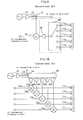
- FIG. 9 is a block diagram showing an example of a conventional transmitter and receiver circuit.
- the transmitter and receiver circuit has a plurality of antennas 11 a to 11 e that receive high-frequency signals, a switch 41 that selects any one of the plurality of antennas 11 a to 11 e , a low-noise amplifier 42 that amplifies high-frequency signals from the selected one of the antennas 11 a to 11 e , a local oscillator 12 that generates local oscillation signals, a power amplifier 13 that amplifies the local oscillation signals, a coupler 14 that divides the amplified local oscillation signals, and a mixer 15 that converts the frequency of the high-frequency signals from the selected one of the antennas 11 a to 11 e in response to the local oscillation signals inputted from the local oscillator 12 .
- the switch 41 is provided in a part of a high-frequency circuit, since the passage loss of the switch 41 cannot be ignored in micro wave or millimetric-wave band, the noise index of the transmitter and receiver circuit is elevated. Whereas, although the loss of the switch 41 can be compensated by installing a low-noise amplifier 42 , the number of components is increased, and the manufacturing costs of the transmitter and receiver circuit are elevated.
- FIG. 10 is a block diagram showing another example of a conventional transmitter and receiver circuit.
- the switch By installing the switch in the local oscillation circuit side instead of installing the switch in the high-frequency circuit side, receiving channels can be switched without increasing the receiving noise.
- a five-way distributor 43 corresponding to the number of mixers 15 a to 15 e must be used.
- a transmitter and receiver circuit has a plurality of antennas for receiving high-frequency signals, a local oscillator for generating local oscillation signals, a plurality of mixers connected to the plurality of antennas, for converting the frequency of the high-frequency signals from corresponding antennas in response to the local oscillation signals inputted from the local oscillator, and a switch for making local oscillation signals generated by the local oscillator input into any one of the plurality of mixers; wherein receiving channels are switched by the switch.
- a transmitter and receiver circuit that requires no power amplifiers to compensate local oscillation signals and no complicated distributors having large loss, and can switch receiving channels without increasing receiving noise can be provided.
- FIG. 1 is a diagram showing a transmitter and receiver circuit according to the first embodiment of the present invention
- FIG. 2 is a circuit diagram showing a switch and a mixer when one mixer is used in a transmitter and receiver circuit according to the first embodiment of the present invention
- FIG. 3 is a diagram showing the dependence of the conversion gain of the single mixer on the power of local oscillation signals
- FIG. 4 is an equivalent circuit schematic of a diode
- FIG. 5 is a circuit diagram showing a switch and a mixer when two mixers are used in a transmitter and receiver circuit according to the first embodiment of the present invention
- FIG. 6 is a diagram showing the dependence of the conversion gain of five parallel mixers wherein five single mixers connected in parallel on the power of local oscillation signals;
- FIG. 7 is a diagram showing a transmitter and receiver circuit according to the second embodiment of the present invention.
- FIG. 8 is a circuit diagram showing a switch and a mixer when two mixers are used in a transmitter and receiver circuit according to the third embodiment of the present invention.
- FIG. 9 is a block diagram showing an example of a conventional transmitter and receiver circuit.
- FIG. 10 is a block diagram showing another example of a conventional transmitter and receiver circuit.
- FIG. 1 is a diagram showing a transmitter and receiver circuit according to the first embodiment of the present invention.
- the transmitter and receiver circuit has a plurality of antennas 11 a to 11 e for receiving high-frequency signals; a local oscillator 12 for generating local oscillation signals; a power amplifier 13 for amplifying the local oscillation signals; a coupler 14 for dividing the amplified local oscillation signals; a plurality of mixers 15 a to 15 e for converting the frequencies of high-frequency signals from corresponding antennas in response to the local oscillation signals inputted from the local oscillator 12 ; and a switch 16 for making the local oscillation signals generated by the local oscillator 12 input into any one of the plurality of mixers 15 a to 15 e.
- the switch 16 is not installed in the high-frequency circuit side, but is installed in the local oscillation circuit side, and the mixers 15 a to 15 e are turned on or off by switching the power levels of the local oscillation signals inputted into the mixers 15 a to 15 e by the switch 16 .
- receiving channels are switched by the switch 16 . Thereby, receiving channels can be switched without increasing receiving noise.
- power amplifiers for compensating local oscillation signals for each of the mixers 15 a to 15 e A complicated distributor having a large loss is not also required.
- FIG. 2 is a circuit diagram showing a switch and a mixer when one mixer is used in a transmitter and receiver circuit according to the first embodiment of the present invention.
- the mixer 15 a is a harmonic mixer using an APDP (anti-parallel diode pair) wherein two diodes are connected in inverse-parallel as mixing elements.
- the mixer 15 a generates the harmonic (higher harmonic wave) components of local oscillation signals based on the non-linearity of the mixing elements, and by the mixing elements, intermediate frequency signals corresponding to the frequency difference between the harmonic components and inputted high-frequency signals are obtained.
- the mixer 15 a has an RF terminal 21 a for inputting high-frequency signals from corresponding antennas; an LO terminal 22 a for inputting local oscillation signals from the local oscillator 12 through the switch 16 ; an IF terminal 23 a for outputting intermediate frequency signals; an APDP 24 a one end of which is connected to the LO terminal 22 a ; a coupled transmission line 25 a one end of which is connected to the RF terminal 21 a and the other end is connected to the other end of the APDP 24 a ; an open stub 26 a connected to the connecting point of the APDP 24 a to the coupled transmission line 25 a ; a short stub 28 a one end of which is connected to the connecting point of the APDP 24 a to the coupled transmission line 25 a , the other end is connected to the IF terminal 23 a , and grounded through a capacitor 27 a ; and a short stub 29 a one end of which is connected to the connecting point of the LO terminal 22
- the open stub 26 a and the short stub 29 a have a length of 1 ⁇ 4 the wavelength of the local oscillation signals, and the short stub 28 a and the coupled transmission line 25 a have a length of 1 ⁇ 4 the wavelength of the high-frequency signals.
- the switch 16 has a switching terminal 31 a for supplying a bias voltage; a diode 32 a whose cathode is grounded and anode is connected to the LO terminal of the mixer 15 a ; an RF choke 33 a one end of which is connected to the switching terminal 31 a , and the other end is connected to the anode of the diode 32 a ; and a transmission line 35 a one end of which is connected to the anode of the diode 32 a through a capacitor 37 a for DC cutting, and the other end is connected to the local oscillator 12 through a capacitor 34 a for DC cutting.
- the transmission line 35 a has a length of 1 ⁇ 4 the length of local oscillation signals.
- the diode 32 a when the diode 32 a is ON, since the other end side of the transmission line 35 a has a high impedance at the frequency of the local oscillation signals by the diode 32 a and the transmission line 35 a , the local oscillation signals are not inputted into the mixer 15 a .
- the diode 32 a when the diode 32 a is OFF, the local oscillation signals are inputted into the mixer 15 a , and intermediate frequency signals are outputted.
- FIG. 3 is a diagram showing the dependence of the conversion gain of the single mixer on the power of local oscillation signals. Normally, the conversion gain of a harmonic mixer becomes constant after sharp increase in the region of low power of the local oscillation signals, thereafter decreases with increase in the local oscillation signals.
- the diode 32 a can be illustrated by a variable resistor 41 and a variable capacitor 42 connected to each other in parallel, and a resistor 43 serially connected thereto.
- the diode 32 a In the low anode voltage region, since the resistance component is small and the capacity component is dominant, the diode 32 a functions as a high-impedance capacitor.
- the diode 32 a In the high anode voltage region of the rising voltage of the diode or higher, since the capacity component is small and the resistance component is dominant, the diode 32 a functions as a low-impedance capacitor. Therefore, the diode functions as a high-impedance capacitor in the region where the local oscillation signals are low, and as a low-impedance resistor in the region where the local oscillation signals are high.
- FIG. 5 is a circuit diagram showing a switch and a mixer when two mixers are used in a transmitter and receiver circuit according to the first embodiment of the present invention. Not only is the mixer 15 a shown in FIG. 2 , but also the mixer 15 b equivalent to the mixer 15 a installed.
- the mixer 15 b has an RF terminal 21 b , an LO terminal 22 b , an IF terminal 23 b , an APDP 24 b , a coupling transmission line 25 b , an open stub 26 b , a capacitor 27 b , and short stubs 28 b and 29 b .
- Each of the open stub 26 b and the short stub 29 b has a length of 1 ⁇ 4 the wavelength of the local oscillation signals; and each of the short stub 28 b and the coupling transmission line 25 b of 1 ⁇ 4 the wavelength of the high-frequency signals.
- the switch 16 has not only a switching terminal 31 a , a diode 32 a , an RF choke 33 a , a capacitor 34 a , and a transmission line 35 a ; but also a switching terminal 31 b for supplying a bias voltage, a diode 32 b whose cathode is grounded and anode is connected to the LO terminal of the corresponding mixer 15 b , an RF choke 33 b one end of which is connected to the switching terminal 31 b and the other end is connected to the anode of the diode 32 b , and a transmission line 35 b one end of which is connected to the anode of the diode 32 b through the capacitor 37 b for DC cutting and the other end is connected to the local oscillator 12 through the capacitor 34 b for DC cutting.
- the transmission line 35 b has a length of 1 ⁇ 4 the wavelength of the local oscillation signals.
- FIG. 6 is a diagram showing the dependence of the conversion gain of five parallel mixers wherein five single mixers connected in parallel on the power of local oscillation signals.
- the curve A indicates a conventional single mixer; the curve B indicates conventional five parallel mixers having no switching terminals; and the curve C indicates five parallel mixers according to the first embodiment.
- the electric power for local oscillation signals of the maximum conversion gain is 6 dBm in the single mixer (curve A); while it is 15 dBm in the conventional five parallel mixers (curve B), 9 dBm higher than that for the single mixer.
- the electric power for local oscillation signals of the maximum conversion gain is equivalent to that for the single mixer even though five mixers are used.
- the conversion gain is not decreased even if local oscillation signals increase, and is maintained constant.
- the transmitter and receiver circuit according to the first embodiment since a high conversion gain can be maintained within a wide range of electric powers for local oscillation signals, the temperature characteristics and manufacturing fluctuation of the output of the local oscillator 12 and the gain of the power amplifier 13 can be absorbed by the mixer.
- a diode is used as the switching element.
- the OFF capacity of the switching element can be lowered, and the loss in the input of local oscillation signals can be reduced.
- a transistor can also be used as the switching element.
- power consumption can be lowered, and the bias circuit can be simplified. It can be formed on the same chip if the same process for the mixing element is used.
- an MEMS (micro electro mechanical systems) switch can also be used. Thereby, the OFF capacity of the switching element can be lowered, the loss in the input of local oscillation signals can be reduced, and power consumption can be lowered. It can be formed on the same chip if the same process for the mixing element is used.
- FIG. 7 is a diagram showing a transmitter and receiver circuit according to the second embodiment of the present invention.
- a port to the transmitting circuit is added to the switch 16 .
- the switch 16 makes local oscillation signals generated by a local oscillator 12 input into any one of a plurality of mixers 15 a to 15 e or a transmitter circuit.
- the receiving channels, and transmission and reception are switched by the switch 16 .
- Other configurations are identical to the configurations of the first embodiment. Thereby, the receiving channels can be switched as in the first embodiment, and the reception mode and the transmission mode can also be switched.
- FIG. 8 is a circuit diagram showing a switch and a mixer when two mixers are used in a transmitter and receiver circuit according to the third embodiment of the present invention.
- the switch 16 has switching terminals 31 a and 31 b for supplying bias voltages; transmission lines 35 a and 35 b installed between the local oscillator 12 and mixers 15 a and 15 b , respectively; transistors 36 a and 36 b , which are switching elements, installed between the connecting points of the transmission lines 35 a and 35 b to the mixers 15 a and 15 b , respectively; and RF chokes 33 a and 33 b each one end of which is connected to the switching terminals 31 a and 31 b , respectively, and each other end of which is connected to the gate of the transistors 36 a and 36 b , respectively.
- Each of the transmission lines 33 a and 35 b has a length of 1 ⁇ 4 the wavelength of the local oscillation signals.
- the mixers 15 a and 15 b are harmonic mixers and the frequency of the local oscillation signals is 1 ⁇ 2 the frequency of the high-frequency signals
- each of the transmission lines 35 a and 35 b has a length of 1 ⁇ 2 the wavelength of the high-frequency signals.
- the length between points Q 1 and Q 2 is the length of one wavelength of the high-frequency signals. Therefore, when the transistor 36 b is ON and the high-frequency signals are short-circuited at the point Q 2 , they are also short-circuited at the point Q 1 one wavelength apart from Q 2 . Thus, the transistor 36 b in the side of the mixer 15 b that is not used is turned on, and a short-circuiting point is generated at the LO terminal 22 a of the mixer 15 a that is used to short-circuit the high-frequency signals. Thereby, in the mixers 15 a and 15 b , since the short stubs 29 a and 29 b shown in FIGS. 2 and 5 in the first embodiment can be omitted, the chip area of the mixers can be reduced.
- harmonic mixer wherein the frequency of local oscillation signals is 1 ⁇ 2 the frequency of high-frequency signals was described in the third embodiment, high-order harmonic mixers wherein the frequency of local oscillation signals is 1 ⁇ 4, 1 ⁇ 6, 1 ⁇ 8 or the like the frequency of high-frequency signals also have the equivalent effect.
Abstract
Description
Claims (6)
Applications Claiming Priority (2)
| Application Number | Priority Date | Filing Date | Title |
|---|---|---|---|
| JP2006272063A JP4708298B2 (en) | 2006-10-03 | 2006-10-03 | Transceiver circuit |
| JP2006-272063 | 2006-10-03 |
Publications (2)
| Publication Number | Publication Date |
|---|---|
| US20080081568A1 US20080081568A1 (en) | 2008-04-03 |
| US7817968B2 true US7817968B2 (en) | 2010-10-19 |
Family
ID=39198547
Family Applications (1)
| Application Number | Title | Priority Date | Filing Date |
|---|---|---|---|
| US11/623,339 Expired - Fee Related US7817968B2 (en) | 2006-10-03 | 2007-01-16 | Transmitter and receiver circuit |
Country Status (3)
| Country | Link |
|---|---|
| US (1) | US7817968B2 (en) |
| JP (1) | JP4708298B2 (en) |
| DE (1) | DE102007019560B4 (en) |
Families Citing this family (7)
| Publication number | Priority date | Publication date | Assignee | Title |
|---|---|---|---|---|
| US8538366B2 (en) | 2007-06-29 | 2013-09-17 | Silicon Laboratories Inc | Rotating harmonic rejection mixer |
| US7756504B2 (en) | 2007-06-29 | 2010-07-13 | Silicon Laboratories Inc. | Rotating harmonic rejection mixer |
| US8260244B2 (en) * | 2007-06-29 | 2012-09-04 | Silicon Laboratories Inc. | Rotating harmonic rejection mixer |
| US8503962B2 (en) * | 2007-06-29 | 2013-08-06 | Silicon Laboratories Inc. | Implementing a rotating harmonic rejection mixer (RHRM) for a TV tuner in an integrated circuit |
| US7860480B2 (en) * | 2007-06-29 | 2010-12-28 | Silicon Laboratories Inc. | Method and apparatus for controlling a harmonic rejection mixer |
| US8571512B2 (en) | 2012-01-05 | 2013-10-29 | Silicon Laboratories Inc. | Implementing a passive rotating harmonic rejection mixer (RHRM) for a TV tuner in an integrated circuit |
| HUE046366T2 (en) * | 2015-12-18 | 2020-03-30 | Gmv Aerospace And Defence S A U | Reconfigurable gnss rf front end and method for reconfiguring a gnss rf front end |
Citations (21)
| Publication number | Priority date | Publication date | Assignee | Title |
|---|---|---|---|---|
| US4494118A (en) * | 1983-08-18 | 1985-01-15 | Hughes Aircraft Company | Direction finding interferometer internal calibration system |
| US5408690A (en) * | 1990-10-01 | 1995-04-18 | Murata Mfg. Co., Ltd. | Antenna supervising apparatus comprising a standing wave ratio measuring unit |
| US5583511A (en) * | 1995-06-06 | 1996-12-10 | Hughes Missile Systems Company | Stepped beam active array antenna and radar system employing same |
| US6100841A (en) * | 1998-06-19 | 2000-08-08 | Raytheon Company | Radio frequency receiving circuit |
| JP2000286601A (en) | 1999-03-30 | 2000-10-13 | Matsushita Electric Ind Co Ltd | High-frequency switch device |
| JP2001007651A (en) | 1999-06-23 | 2001-01-12 | Mitsubishi Electric Corp | Frequency conversion mixer |
| EP1152254A2 (en) | 2000-04-25 | 2001-11-07 | Agilent Technologies, Inc. (a Delaware corporation) | Combined GPS and CDMA in a mobile transceiver |
| US20030022644A1 (en) * | 2001-07-26 | 2003-01-30 | Takao Imai | Satellite receiving converter and satellite receiving system |
| US20030045262A1 (en) * | 2001-09-04 | 2003-03-06 | Vaughan Mark J. | Waveguide mixer/coupler |
| JP2003078303A (en) | 2001-08-31 | 2003-03-14 | Murata Mfg Co Ltd | Switch circuit |
| US6704818B1 (en) * | 2000-12-29 | 2004-03-09 | Intel Corporation | Voltage-mode driver with pre-emphasis, slew-rate control and source termination |
| US20050064840A1 (en) * | 2003-05-30 | 2005-03-24 | The Regents Of The University Of California | Wideband distributed mixers |
| US20050141602A1 (en) * | 2003-12-26 | 2005-06-30 | Seok-Bong Hyun | Pulse signal generator for ultra-wideband radio transception and radio transceiver having the same |
| US20050140470A1 (en) * | 2000-08-24 | 2005-06-30 | Mitsubishi Denki Kabushiki Kaisha | High frequency module |
| US20050190099A1 (en) * | 2002-02-27 | 2005-09-01 | Hitachi, Ltd. | Monopulse radar system |
| DE10345971B4 (en) | 2003-10-02 | 2005-12-22 | Siemens Ag | Mobile transceiver |
| US20050285541A1 (en) * | 2003-06-23 | 2005-12-29 | Lechevalier Robert E | Electron beam RF amplifier and emitter |
| JP2006050472A (en) | 2004-08-09 | 2006-02-16 | Mitsubishi Electric Corp | Mixer circuit |
| US7072613B2 (en) * | 2004-02-25 | 2006-07-04 | Matsushita Electric Industrial Co., Ltd. | Wireless communication medium processing apparatus and wireless communication medium processing system |
| US20070207761A1 (en) * | 2005-12-16 | 2007-09-06 | Honeywell International Inc. | Mems based multiband receiver architecture |
| US7697632B2 (en) * | 2003-12-29 | 2010-04-13 | Freescale Semiconductor, Inc. | Low IF radio receiver |
Family Cites Families (7)
| Publication number | Priority date | Publication date | Assignee | Title |
|---|---|---|---|---|
| JP2750781B2 (en) * | 1990-11-13 | 1998-05-13 | 本田技研工業 株式会社 | FM radar |
| JP2665834B2 (en) * | 1991-02-15 | 1997-10-22 | 本田技研工業株式会社 | FM radar |
| JP2989428B2 (en) * | 1993-06-17 | 1999-12-13 | 本田技研工業株式会社 | Time-sharing FM radar system |
| JPH0933637A (en) * | 1995-07-25 | 1997-02-07 | Denso Corp | Radar device |
| JP3884958B2 (en) * | 1999-10-13 | 2007-02-21 | 株式会社日立製作所 | Communication terminal, in-vehicle communication terminal, and vehicle using the same |
| JP3920061B2 (en) * | 2001-09-26 | 2007-05-30 | シャープ株式会社 | Local oscillation signal distributor and low noise converter using the same |
| JP2006186718A (en) * | 2004-12-28 | 2006-07-13 | Matsushita Electric Ind Co Ltd | Radio receiving device, radio transmitting and receiving device, and mobile terminal device |
-
2006
- 2006-10-03 JP JP2006272063A patent/JP4708298B2/en not_active Expired - Fee Related
-
2007
- 2007-01-16 US US11/623,339 patent/US7817968B2/en not_active Expired - Fee Related
- 2007-04-25 DE DE102007019560.7A patent/DE102007019560B4/en not_active Expired - Fee Related
Patent Citations (24)
| Publication number | Priority date | Publication date | Assignee | Title |
|---|---|---|---|---|
| US4494118A (en) * | 1983-08-18 | 1985-01-15 | Hughes Aircraft Company | Direction finding interferometer internal calibration system |
| US5408690A (en) * | 1990-10-01 | 1995-04-18 | Murata Mfg. Co., Ltd. | Antenna supervising apparatus comprising a standing wave ratio measuring unit |
| US5583511A (en) * | 1995-06-06 | 1996-12-10 | Hughes Missile Systems Company | Stepped beam active array antenna and radar system employing same |
| US6100841A (en) * | 1998-06-19 | 2000-08-08 | Raytheon Company | Radio frequency receiving circuit |
| JP2000286601A (en) | 1999-03-30 | 2000-10-13 | Matsushita Electric Ind Co Ltd | High-frequency switch device |
| JP2001007651A (en) | 1999-06-23 | 2001-01-12 | Mitsubishi Electric Corp | Frequency conversion mixer |
| EP1152254A2 (en) | 2000-04-25 | 2001-11-07 | Agilent Technologies, Inc. (a Delaware corporation) | Combined GPS and CDMA in a mobile transceiver |
| US6351236B1 (en) | 2000-04-25 | 2002-02-26 | Agilent Technologies, Inc. | Combined GPS and CDMA in a mobile transceiver |
| US20070120732A1 (en) * | 2000-08-24 | 2007-05-31 | Mitsubishi Denki Kabushiki Kaisha | High frequency module |
| US20050140470A1 (en) * | 2000-08-24 | 2005-06-30 | Mitsubishi Denki Kabushiki Kaisha | High frequency module |
| US6704818B1 (en) * | 2000-12-29 | 2004-03-09 | Intel Corporation | Voltage-mode driver with pre-emphasis, slew-rate control and source termination |
| US20030022644A1 (en) * | 2001-07-26 | 2003-01-30 | Takao Imai | Satellite receiving converter and satellite receiving system |
| JP2003078303A (en) | 2001-08-31 | 2003-03-14 | Murata Mfg Co Ltd | Switch circuit |
| US20030045262A1 (en) * | 2001-09-04 | 2003-03-06 | Vaughan Mark J. | Waveguide mixer/coupler |
| US20050190099A1 (en) * | 2002-02-27 | 2005-09-01 | Hitachi, Ltd. | Monopulse radar system |
| US20050064840A1 (en) * | 2003-05-30 | 2005-03-24 | The Regents Of The University Of California | Wideband distributed mixers |
| US20050285541A1 (en) * | 2003-06-23 | 2005-12-29 | Lechevalier Robert E | Electron beam RF amplifier and emitter |
| DE10345971B4 (en) | 2003-10-02 | 2005-12-22 | Siemens Ag | Mobile transceiver |
| US20050141602A1 (en) * | 2003-12-26 | 2005-06-30 | Seok-Bong Hyun | Pulse signal generator for ultra-wideband radio transception and radio transceiver having the same |
| US7508860B2 (en) * | 2003-12-26 | 2009-03-24 | Electronics And Telecommunications Research Institute | Pulse signal generator for ultra-wideband radio transception and radio transceiver having the same |
| US7697632B2 (en) * | 2003-12-29 | 2010-04-13 | Freescale Semiconductor, Inc. | Low IF radio receiver |
| US7072613B2 (en) * | 2004-02-25 | 2006-07-04 | Matsushita Electric Industrial Co., Ltd. | Wireless communication medium processing apparatus and wireless communication medium processing system |
| JP2006050472A (en) | 2004-08-09 | 2006-02-16 | Mitsubishi Electric Corp | Mixer circuit |
| US20070207761A1 (en) * | 2005-12-16 | 2007-09-06 | Honeywell International Inc. | Mems based multiband receiver architecture |
Non-Patent Citations (2)
| Title |
|---|
| Itoh et al., A 40 GHz Band Monolithic Even Harmonic Mixer With an Antiparallel Diode Pair, 1999 IEEE MTTS Int. Microwave Symp. Dig., pp. 879-882, 1991. |
| Kanaya et al., A 94 GHz High Performance Quadruple Subharmortio Mixer MMIC, 2002 IEEE MTT-S Int. Microwave Symp. Dig., pp. 1249-1252, 2002. |
Also Published As
| Publication number | Publication date |
|---|---|
| DE102007019560A1 (en) | 2008-04-24 |
| JP2008092360A (en) | 2008-04-17 |
| US20080081568A1 (en) | 2008-04-03 |
| JP4708298B2 (en) | 2011-06-22 |
| DE102007019560B4 (en) | 2014-02-13 |
Similar Documents
| Publication | Publication Date | Title |
|---|---|---|
| US7817968B2 (en) | Transmitter and receiver circuit | |
| US8340606B2 (en) | Doherty amplifier and transmitter using mixer | |
| EP0700169B1 (en) | Transmit-receive switch circuit for radiocommunication apparatus | |
| US7428230B2 (en) | Time-division-duplexing type power amplification module | |
| US7839237B2 (en) | Phase shifter with flexible control voltage | |
| KR100196241B1 (en) | Microwave mixing circuit | |
| US8467739B2 (en) | Monolithic integrated transceiver | |
| KR20010053413A (en) | Mobile telephone system | |
| CN110784179B (en) | Double-balance FET mixer | |
| US20050107043A1 (en) | Integration of diversity switch in combination with a T/R switch for a radio transceiver on a single chip | |
| US7511592B2 (en) | Switch circuit and integrated circuit | |
| US20090011720A1 (en) | Bidirectional Frequency Converter and Radio Equipment Using Same | |
| US20110171994A1 (en) | Multi-mode transceiver and a circuit for operating the multi-mode transceiver | |
| KR101543818B1 (en) | Front end for rf transmitting-receiving systems with implicit directional control and time-multiplexing method in submicron technology | |
| US6960959B2 (en) | Power amplifier and communication apparatus | |
| US8948714B2 (en) | Low noise converter of satellite broadcasting receiver | |
| US7420424B2 (en) | Power amplifier transmission line transformer | |
| EP1649476B1 (en) | Radiofrequency double pole single throw switch | |
| EP2210338B1 (en) | Mixer architecture | |
| US20210384931A1 (en) | Wideband receivers and methods of operation | |
| JPH0955681A (en) | Time division duplex transmitter-receiver | |
| KR100449431B1 (en) | A power amplifier of the portable phone | |
| KR100318916B1 (en) | Power amplifier controling apparatus of multi-band frequency processing radio terminal | |
| JPH11127034A (en) | Single-balanced mixer | |
| KR20040016588A (en) | Power amplifier module for possiblie switching of input/output mode |
Legal Events
| Date | Code | Title | Description |
|---|---|---|---|
| AS | Assignment |
Owner name: MITSUBISHI ELECTRIC CORPORATION, JAPAN Free format text: ASSIGNMENT OF ASSIGNORS INTEREST;ASSIGNOR:KANAYA, KO;REEL/FRAME:018759/0483 Effective date: 20061214 |
|
| STCF | Information on status: patent grant |
Free format text: PATENTED CASE |
|
| FEPP | Fee payment procedure |
Free format text: PAYOR NUMBER ASSIGNED (ORIGINAL EVENT CODE: ASPN); ENTITY STATUS OF PATENT OWNER: LARGE ENTITY |
|
| FPAY | Fee payment |
Year of fee payment: 4 |
|
| MAFP | Maintenance fee payment |
Free format text: PAYMENT OF MAINTENANCE FEE, 8TH YEAR, LARGE ENTITY (ORIGINAL EVENT CODE: M1552) Year of fee payment: 8 |
|
| FEPP | Fee payment procedure |
Free format text: MAINTENANCE FEE REMINDER MAILED (ORIGINAL EVENT CODE: REM.); ENTITY STATUS OF PATENT OWNER: LARGE ENTITY |
|
| LAPS | Lapse for failure to pay maintenance fees |
Free format text: PATENT EXPIRED FOR FAILURE TO PAY MAINTENANCE FEES (ORIGINAL EVENT CODE: EXP.); ENTITY STATUS OF PATENT OWNER: LARGE ENTITY |
|
| STCH | Information on status: patent discontinuation |
Free format text: PATENT EXPIRED DUE TO NONPAYMENT OF MAINTENANCE FEES UNDER 37 CFR 1.362 |
|
| FP | Lapsed due to failure to pay maintenance fee |
Effective date: 20221019 |