US7826243B2 - Multiple chip module and package stacking for storage devices - Google Patents
Multiple chip module and package stacking for storage devices Download PDFInfo
- Publication number
- US7826243B2 US7826243B2 US11/322,442 US32244205A US7826243B2 US 7826243 B2 US7826243 B2 US 7826243B2 US 32244205 A US32244205 A US 32244205A US 7826243 B2 US7826243 B2 US 7826243B2
- Authority
- US
- United States
- Prior art keywords
- module
- passive
- modules
- stacked
- serial chain
- Prior art date
- Legal status (The legal status is an assumption and is not a legal conclusion. Google has not performed a legal analysis and makes no representation as to the accuracy of the status listed.)
- Active, expires
Links
Images


Classifications
-
- H—ELECTRICITY
- H01—ELECTRIC ELEMENTS
- H01L—SEMICONDUCTOR DEVICES NOT COVERED BY CLASS H10
- H01L23/00—Details of semiconductor or other solid state devices
- H01L23/02—Containers; Seals
-
- H—ELECTRICITY
- H01—ELECTRIC ELEMENTS
- H01L—SEMICONDUCTOR DEVICES NOT COVERED BY CLASS H10
- H01L25/00—Assemblies consisting of a plurality of individual semiconductor or other solid state devices ; Multistep manufacturing processes thereof
- H01L25/03—Assemblies consisting of a plurality of individual semiconductor or other solid state devices ; Multistep manufacturing processes thereof all the devices being of a type provided for in the same subgroup of groups H01L27/00 - H01L33/00, or in a single subclass of H10K, H10N, e.g. assemblies of rectifier diodes
- H01L25/10—Assemblies consisting of a plurality of individual semiconductor or other solid state devices ; Multistep manufacturing processes thereof all the devices being of a type provided for in the same subgroup of groups H01L27/00 - H01L33/00, or in a single subclass of H10K, H10N, e.g. assemblies of rectifier diodes the devices having separate containers
- H01L25/105—Assemblies consisting of a plurality of individual semiconductor or other solid state devices ; Multistep manufacturing processes thereof all the devices being of a type provided for in the same subgroup of groups H01L27/00 - H01L33/00, or in a single subclass of H10K, H10N, e.g. assemblies of rectifier diodes the devices having separate containers the devices being of a type provided for in group H01L27/00
-
- H—ELECTRICITY
- H01—ELECTRIC ELEMENTS
- H01L—SEMICONDUCTOR DEVICES NOT COVERED BY CLASS H10
- H01L23/00—Details of semiconductor or other solid state devices
- H01L23/12—Mountings, e.g. non-detachable insulating substrates
-
- H—ELECTRICITY
- H01—ELECTRIC ELEMENTS
- H01L—SEMICONDUCTOR DEVICES NOT COVERED BY CLASS H10
- H01L25/00—Assemblies consisting of a plurality of individual semiconductor or other solid state devices ; Multistep manufacturing processes thereof
- H01L25/03—Assemblies consisting of a plurality of individual semiconductor or other solid state devices ; Multistep manufacturing processes thereof all the devices being of a type provided for in the same subgroup of groups H01L27/00 - H01L33/00, or in a single subclass of H10K, H10N, e.g. assemblies of rectifier diodes
- H01L25/04—Assemblies consisting of a plurality of individual semiconductor or other solid state devices ; Multistep manufacturing processes thereof all the devices being of a type provided for in the same subgroup of groups H01L27/00 - H01L33/00, or in a single subclass of H10K, H10N, e.g. assemblies of rectifier diodes the devices not having separate containers
- H01L25/065—Assemblies consisting of a plurality of individual semiconductor or other solid state devices ; Multistep manufacturing processes thereof all the devices being of a type provided for in the same subgroup of groups H01L27/00 - H01L33/00, or in a single subclass of H10K, H10N, e.g. assemblies of rectifier diodes the devices not having separate containers the devices being of a type provided for in group H01L27/00
- H01L25/0655—Assemblies consisting of a plurality of individual semiconductor or other solid state devices ; Multistep manufacturing processes thereof all the devices being of a type provided for in the same subgroup of groups H01L27/00 - H01L33/00, or in a single subclass of H10K, H10N, e.g. assemblies of rectifier diodes the devices not having separate containers the devices being of a type provided for in group H01L27/00 the devices being arranged next to each other
-
- H—ELECTRICITY
- H01—ELECTRIC ELEMENTS
- H01L—SEMICONDUCTOR DEVICES NOT COVERED BY CLASS H10
- H01L2224/00—Indexing scheme for arrangements for connecting or disconnecting semiconductor or solid-state bodies and methods related thereto as covered by H01L24/00
- H01L2224/01—Means for bonding being attached to, or being formed on, the surface to be connected, e.g. chip-to-package, die-attach, "first-level" interconnects; Manufacturing methods related thereto
- H01L2224/10—Bump connectors; Manufacturing methods related thereto
- H01L2224/15—Structure, shape, material or disposition of the bump connectors after the connecting process
- H01L2224/16—Structure, shape, material or disposition of the bump connectors after the connecting process of an individual bump connector
-
- H—ELECTRICITY
- H01—ELECTRIC ELEMENTS
- H01L—SEMICONDUCTOR DEVICES NOT COVERED BY CLASS H10
- H01L2225/00—Details relating to assemblies covered by the group H01L25/00 but not provided for in its subgroups
- H01L2225/03—All the devices being of a type provided for in the same subgroup of groups H01L27/00 - H01L33/648 and H10K99/00
- H01L2225/10—All the devices being of a type provided for in the same subgroup of groups H01L27/00 - H01L33/648 and H10K99/00 the devices having separate containers
- H01L2225/1005—All the devices being of a type provided for in the same subgroup of groups H01L27/00 - H01L33/648 and H10K99/00 the devices having separate containers the devices being of a type provided for in group H01L27/00
- H01L2225/1011—All the devices being of a type provided for in the same subgroup of groups H01L27/00 - H01L33/648 and H10K99/00 the devices having separate containers the devices being of a type provided for in group H01L27/00 the containers being in a stacked arrangement
- H01L2225/1017—All the devices being of a type provided for in the same subgroup of groups H01L27/00 - H01L33/648 and H10K99/00 the devices having separate containers the devices being of a type provided for in group H01L27/00 the containers being in a stacked arrangement the lowermost container comprising a device support
- H01L2225/1023—All the devices being of a type provided for in the same subgroup of groups H01L27/00 - H01L33/648 and H10K99/00 the devices having separate containers the devices being of a type provided for in group H01L27/00 the containers being in a stacked arrangement the lowermost container comprising a device support the support being an insulating substrate
-
- H—ELECTRICITY
- H01—ELECTRIC ELEMENTS
- H01L—SEMICONDUCTOR DEVICES NOT COVERED BY CLASS H10
- H01L2225/00—Details relating to assemblies covered by the group H01L25/00 but not provided for in its subgroups
- H01L2225/03—All the devices being of a type provided for in the same subgroup of groups H01L27/00 - H01L33/648 and H10K99/00
- H01L2225/10—All the devices being of a type provided for in the same subgroup of groups H01L27/00 - H01L33/648 and H10K99/00 the devices having separate containers
- H01L2225/1005—All the devices being of a type provided for in the same subgroup of groups H01L27/00 - H01L33/648 and H10K99/00 the devices having separate containers the devices being of a type provided for in group H01L27/00
- H01L2225/1011—All the devices being of a type provided for in the same subgroup of groups H01L27/00 - H01L33/648 and H10K99/00 the devices having separate containers the devices being of a type provided for in group H01L27/00 the containers being in a stacked arrangement
- H01L2225/1047—Details of electrical connections between containers
- H01L2225/1058—Bump or bump-like electrical connections, e.g. balls, pillars, posts
-
- H—ELECTRICITY
- H01—ELECTRIC ELEMENTS
- H01L—SEMICONDUCTOR DEVICES NOT COVERED BY CLASS H10
- H01L24/00—Arrangements for connecting or disconnecting semiconductor or solid-state bodies; Methods or apparatus related thereto
- H01L24/01—Means for bonding being attached to, or being formed on, the surface to be connected, e.g. chip-to-package, die-attach, "first-level" interconnects; Manufacturing methods related thereto
- H01L24/10—Bump connectors ; Manufacturing methods related thereto
- H01L24/15—Structure, shape, material or disposition of the bump connectors after the connecting process
- H01L24/16—Structure, shape, material or disposition of the bump connectors after the connecting process of an individual bump connector
-
- H—ELECTRICITY
- H01—ELECTRIC ELEMENTS
- H01L—SEMICONDUCTOR DEVICES NOT COVERED BY CLASS H10
- H01L25/00—Assemblies consisting of a plurality of individual semiconductor or other solid state devices ; Multistep manufacturing processes thereof
- H01L25/18—Assemblies consisting of a plurality of individual semiconductor or other solid state devices ; Multistep manufacturing processes thereof the devices being of types provided for in two or more different subgroups of the same main group of groups H01L27/00 - H01L33/00, or in a single subclass of H10K, H10N
-
- H—ELECTRICITY
- H01—ELECTRIC ELEMENTS
- H01L—SEMICONDUCTOR DEVICES NOT COVERED BY CLASS H10
- H01L2924/00—Indexing scheme for arrangements or methods for connecting or disconnecting semiconductor or solid-state bodies as covered by H01L24/00
- H01L2924/01—Chemical elements
- H01L2924/01079—Gold [Au]
-
- H—ELECTRICITY
- H01—ELECTRIC ELEMENTS
- H01L—SEMICONDUCTOR DEVICES NOT COVERED BY CLASS H10
- H01L2924/00—Indexing scheme for arrangements or methods for connecting or disconnecting semiconductor or solid-state bodies as covered by H01L24/00
- H01L2924/15—Details of package parts other than the semiconductor or other solid state devices to be connected
- H01L2924/151—Die mounting substrate
- H01L2924/153—Connection portion
- H01L2924/1532—Connection portion the connection portion being formed on the die mounting surface of the substrate
- H01L2924/1533—Connection portion the connection portion being formed on the die mounting surface of the substrate the connection portion being formed both on the die mounting surface of the substrate and outside the die mounting surface of the substrate
- H01L2924/15331—Connection portion the connection portion being formed on the die mounting surface of the substrate the connection portion being formed both on the die mounting surface of the substrate and outside the die mounting surface of the substrate being a ball array, e.g. BGA
-
- H—ELECTRICITY
- H01—ELECTRIC ELEMENTS
- H01L—SEMICONDUCTOR DEVICES NOT COVERED BY CLASS H10
- H01L2924/00—Indexing scheme for arrangements or methods for connecting or disconnecting semiconductor or solid-state bodies as covered by H01L24/00
- H01L2924/15—Details of package parts other than the semiconductor or other solid state devices to be connected
- H01L2924/161—Cap
- H01L2924/162—Disposition
- H01L2924/1627—Disposition stacked type assemblies, e.g. stacked multi-cavities
Definitions
- the present invention relates to computer systems. More particularly, the present invention relates to flash memory based semiconductor disk drives and a method of using multiple chip module (MCM) and Package Stacking technique to support miniaturization and memory scalability.
- MCM multiple chip module
- a flash memory based semiconductor disk drive typically use separate packages for the interface controller, the DMA controller, the processor and separate packages for the Flash devices, the FPROMs and the RAMs. This current method limits the miniaturization of the entire storage device.
- chip modules and packages need to be stacked. Stacking both on chip module and package level maximizes the capacity in a limited area thus realizing the move to miniaturize the entire storage device.
- a technique in stacking chip modules and packages strategically to support miniaturization and memory scalability in both vertical and horizontal orientation is therefore proposed.
- semiconductor dies are mounted in a module to become a MCM which serves as the basic building block.
- MCM which serves as the basic building block.
- Combination of these modules and dies in a substrate creates a package with specific function or a range of memory capacity.
- These packages are stacked to increase capacity or add functions.
- a combination of different existing technology such as flip chip, wire bond, MCM, module stacking, advance packaging, etc. are used to accomplish highly reliable module to module and package to package interconnection and scalability.
- a single package can have a wide range of capacity depending on the memory capacity of the die used and the number of modules stacked within the package.
- the stacked modules in a package serve as the building blocks for the package level stacking.
- the present invention takes advantage of the existing stacking technology both on the module and package level. This maximizes the capacity in a small area, realizing the miniaturization transition. Modular approach is used in creating basic building blocks which can be tested individually and replaced easily prior to final packaging, making the technique reliable, and cost effective. A wide range of capacity can be configured through variation of die capacities and stacking modules and/or packages. Expanding capacity may be implemented vertically, horizontally or both, depending on board area and desired capacity.
- FIG. 1 a shows the block diagram of the stackable system for high performance, high capacity devices according to an example embodiment of the present invention.
- FIG. 1 b shows the block diagram of the stackable system for lower performance, lower capacity devices according to an example embodiment of the present invention.
- FIG. 2 a , 2 b , 2 c depict the SDRAM module's top and bottom drawings and a cross sectional representation of stacked multiple SDRAM modules according to an example embodiment of the present invention.
- FIG. 3 a , 3 b , 3 c depict the flash module's top and bottom drawings and a cross sectional representation of stacked multiple flash modules according to an example embodiment of the present invention.
- FIG. 4 a , 4 b depict the first high-end controller module's top and bottom drawings according to an example embodiment of the present invention.
- FIG. 5 a , 5 b depict the memory module's top and bottom drawings according to an example embodiment of the present invention.
- FIG. 6 a , 6 b depict the first low-end controller module's top and bottom drawings according to an example embodiment of the present invention.
- FIG. 7 a , 7 b depict the second high-end controller module's top and bottom drawings according to an example embodiment of the present invention.
- FIG. 8 a , 8 b depict the second low-end controller module's top and bottom drawings according to an example embodiment of the present invention.
- FIG. 9 depicts the stacked SDRAM modules further stacked on the controller module according to an example embodiment of the present invention. This configuration is used for high end applications. The figure also shows how the balls have corresponding pads for inter-module connection.
- FIG. 10 depicts stacked flash modules further stacked on the memory module according to an example embodiment of the present invention. The figure also shows how the balls have corresponding pads for inter-module connection.
- FIG. 11 depicts the possible stacking options for the first high-end controller module and the memory modules according to an example embodiment of the present invention.
- a substrate interface is used to attach one group of stacked modules to another.
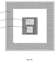
- FIG. 12 a is an isometric exploded drawing of the stacking technique presented in FIG. 11 according to an example embodiment of the present invention. Multiple identical stacking is not included in this drawing.
- FIG. 12 b is another package stacking technique using Pin Grid Array (PGA) rather than Ball Grid Array (BGA) according to an example embodiment of the present invention. This is used for easy replacement and expansion.
- PGA Pin Grid Array
- BGA Ball Grid Array
- FIG. 13 depicts the low-end controller module configuration with stacked flash module according to an example embodiment of the present invention. The figure also shows how the balls have corresponding pads for inter-module connection.
- FIG. 14 is an isometric exploded version of the stacking technique presented in FIG. 11 according to an example embodiment of the present invention.
- FIG. 15 a , 15 b depict the second high-end controller module configuration with stacked memory modules according to an example embodiment of the present invention.
- the figures also show how the balls have corresponding pads for inter-module connection.
- FIG. 16 is an isometric exploded version of the stacking technique presented in FIG. 14 according to an example embodiment of the present invention.
- FIG. 17 a , 17 b depict the second low-end controller module configuration with stacked memory modules according to an example embodiment of the present invention.
- the figures also show how the balls have corresponding pads for inter-module connection.
- FIG. 18 is an isometric exploded version of the stacking technique presented in FIG. 17 according to an example embodiment of the present invention.
- FIG. 19 shows a pin assignment and connection technique to be able to select specific layer in a multi-stacked module according to an example embodiment of the present invention.
- FIG. 20 a shows another pin assignment technique which uses a rotational stacking orientation to allow stacking of four identical modules representing different bus interfaces according to an example embodiment of the present invention.
- FIG. 20 b shows a cross-section representation of the four stacked modules on a rotational stacking technique and how their pins mates according to an example embodiment of the present invention.
- FIG. 21 a shows another pin assignment and connection technique to be able to connect a serial chain route from multiple modules in a stack according to an example embodiment of the present invention.
- FIG. 21 b shows the routing of a serial chain connection from one stack location to another allowing application of both vertical and horizontal expansion independently or simultaneously according to an example embodiment of the present invention.
- FIG. 1 a is a block diagram of a flash storage system according to a first example embodiment of the present invention.
- the block diagram shows the entire high-end system that is modularized, stacked, and packaged to achieve the desired features of the technique.
- the heart of the system is the main controller-processor 101 which interfaces with the flash memory, the flash PROM and the SDRAM memory blocks.
- the SDRAM is configured from a single bank 102 to a maximum of four banks depending on the desired capacity. Each bank such as 102 includes 3 SDRAMs.
- the flash devices such as 107 are controlled by the Flash Interface Controller such as 105 .
- Each controller supports four flash buses such as flash bus A11 106 , and each flash bus supports a maximum of 8 flash devices.
- the main controller-processor supports four flash interface controllers through 4 different busses such as B bus 104 .
- the four flash interface controllers with their corresponding flash devices comprise the memory set 108 .
- the main controller-processor can support from one memory set to a maximum of 15 memory sets. This is a maximum support of 1,920 flash devices.
- FIG. 1 b is a block diagram of a flash storage system according to a second example embodiment of the present invention.
- the block diagram shows the entire low-end system that is modularized, stacked, and packaged to achieve the desired features of the technique. Since a low-end system may not require a large amount of memory capacity, SDRAM may be limited to one bank 109 , or none at all, and the supported flash devices may also be limited to only two sets of flash buses.
- One set of flash buses 110 consists of four flash bus with 8 flash devices supported per flash bus, which results in a maximum supported number of 64 flash devices.
- FIG. 2 a is a top view of an SDRAM module
- three SDRAM dies 201 are placed in a single substrate 203 to become the SDRAM module which is one of the basic building blocks.
- the SDRAM module is represented in FIG. 1 as a single bank 102 composed of SDRAM 00, SDRAM 01, and SDRAM 02 connected to the SDRAM interface 103 . All signals needed to interface to the controller module and other SDRAM modules are assigned in both the bottom balls 204 and top pads 202 respectively. Bottom balls 204 are shown in FIG.
- FIG. 2 b which is a bottom view of the SDRAM module, three slots 205 are created under the SDRAM die's pad attach area to accommodate bottom wire bonding.
- FIG. 2 c is the stacked module cross sectional representation. Top pads 202 and bottom balls 204 act as the vertical interconnects between all SDRAM modules and to the controller module. Varying the SDRAM die capacity and the stack quantity, results in wide range of total SDRAM capacity depending on the product application.
- the SDRAM device organization, capacity and bank limitations are defined by the main controller-processor's SDRAM interface specifications.
- the main controller-processor intended to be used for this example embodiment of the present invention supports a 32-bit wide 4 banks maximum SDRAM configuration.
- FIG. 3 a is a top view that shows four flash dies 301 in a single substrate 303 that collectively form part of a flash module, which can also function as a basic building block. All signals needed to interface with the memory module and other flash modules are assigned in both the bottom balls 304 and the top pads 302 , respectively, as shown in FIGS. 3 a , 3 b and 3 c .
- the flash modules are stacked. Maximum stack quantity depends on the flash interface controller specifications. Top pads 302 and bottom balls 304 acts as the vertical interconnects between stacked flash modules and to the memory module. Varying the flash die capacity and the stacking quantity, results in a wide range of total flash capacity depending on the product application and capacity requirements.
- the flash device organization and capacity limitations are defined by the flash interface controller's specifications.
- the flash interface controller intended to be used for this used for this example embodiment of the present invention supports 8 flash devices per flash bus, thus allowing a maximum stacking of 8 flash modules.
- FIG. 4 a shows the top view of the first example embodiment of the present invention illustrated in a first high-end controller module configuration.
- a single FPROM die 401 is placed at the center of the substrate 404 .
- Pads are composed of two sections, one for the SDRAM module interface shown as 402 and another for the memory module interface shown as 403 . This technique enables multiple stacking of both SDRAM modules and memory modules in a single package.
- FIG. 4 b shows the bottom view of the controller module.
- a single main controller-processor die 406 is placed at the center of the substrate.
- the controller module becomes a base module for the package.
- the balls 405 are used to connect to the main substrate which is typically a printed circuit board (PCB).
- PCB printed circuit board
- FIG. 5 a shows the top view of the memory module which is also a basic building block.
- a single flash interface controller die 501 is placed on the center of the substrate 504 .
- Pads are composed of two sections, one for the flash module interface shown as 502 and another for the other memory module interface shown as 503 .
- This technique enables multiple stacking of flash modules and memory modules in a single package.
- the memory module becomes a base module for the package.
- FIG. 5 b shows the bottom view of the memory module.
- the memory module balls 505 are used to connect to the main substrate PCB, to the controller modules or to the other memory modules depending on the type of configuration desired.
- FIG. 6 a shows the top view of the second example embodiment of the present invention illustrated in a first low-end controller module configuration.
- Two SDRAMs 601 and a single FPROM 602 are placed on top of the module. This configuration is flexible. The SDRAMs can be unpopulated in a low performance application. Internal SRAMs in the main controller-processor will take over the SDRAM functions.
- the main controller-processor 605 is placed at the bottom of the module. This configuration does not allow stacking of the SDRAM which is not necessary for low capacity applications. Flash modules are stacked on top, interfacing to the pads 603 .
- the substrate 604 is the same size as the flash module making its final package smaller.
- the bottom balls 606 are used to interface with the main PCB.
- FIG. 7 a shows the top view of the first example embodiment of the present invention illustrated in a second high-end controller module configuration, where four memory modules 701 can be mounted on separate locations adjacent to each other.
- Memory module interface pads 704 are allocated for multiple stack configurations.
- 3 SDRAM dies 702 are mounted.
- Each area corresponds to one SDRAM bank 703 , totaling to a maximum of 4 SDRAM banks in the package.
- the bottom view is presented in FIG. 7 b , where the main controller-processor die 705 and the FPROM die 706 are mounted adjacent to each other.
- the module's balls 707 are used for external interface to the main PCB.
- FIG. 8 a shows the top view of the second example embodiment of the present invention illustrated in a second low-end controller module configuration, where only two memory modules 801 can be mounted side-by-side.
- Memory module interface pads 802 are allocated for multiple stacking configurations.
- 3 SDRAM dies 803 are mounted.
- Each area corresponds to one SDRAM bank 804 , totaling to only a maximum of 2 SDRAM banks in a package.
- the SDRAM can either be mounted or not depending on the application. Internal SRAMs can also be used instead of the SDRAMs.
- the stacked memory modules can also be configured to support both internal and external flash interface controller applications.
- the bottom view is presented in FIG. 8 b , where the main controller-processor die 805 and the FPROM die 806 are mounted adjacent to each other.
- the module balls 807 are used for external interface to the main PCB.
- FIG. 9 shows the stacking of SDRAM module 901 and controller module 902 .
- a single or stacked SDRAM module can be placed on top of a controller module.
- the pads for the SDRAM module interface 903 must align with the SDRAM module balls 904 .
- the bottom-most SDRAM module 905 serves as bank 0, and the top-most module 906 serves as bank 3.
- the outer pads 907 are for the memory module interface.
- FIG. 10 shows the stacking of flash modules 1001 and memory module 1002 .
- a four-stack or eight-stack flash module is placed on top of a memory module.
- the pads for the flash module interface 1003 must align with the flash module balls 1004 .
- the outer pads 1005 are for other memory module interface.
- the flash interface controller intended to be used for this example embodiment of the present invention supports a maximum of 4 flash buses and each flash bus supports a maximum of 8 flash devices.
- the bottom-most flash module 1006 contains the 4 flash buses' Flash 00 devices and the top-most module 1007 contains the 4 flash buses' Flash 07 devices.
- FIG. 11 shows a sample of a maximized stacking technique that can be configured through vertical, horizontal or combined expansion. Multiple staking will increase the overall height of the module, thus requiring a filler 1101 to physically interconnect two stacked modules. A thinner filler 1102 may be used depending on the height differential between the modules which is dependent to the number of stacks applied.
- a controller module with the stacked SDRAM modules act as the controller package 1103 .
- a memory module with stacked flash modules acts as the memory package 1104 .
- Four memory packages stacked together form the memory set 1105 . Vertical expansion happens when the controller package is stacked with a single or multiple memory sets. The figure shows a single memory set to be stacked to the controller package.
- Horizontal expansion happens when the controller package is located on a different site on the PCB relative to the memory sets. Also multiple memory sets can be located on different sites on a PCB. Combo expansion happens when both vertical and horizontal expansion technique is implemented simultaneously. The expansion technique is very flexible depending on the desired memory capacity, main PCB size limitations and also height limitations.
- FIG. 12 a shows the isometric and exploded drawing of the stacking technique for the first high-end controller configuration. Pins are assigned strategically and modules are stacked to make possible the miniaturization of the entire system in a package.
- FIG. 12 b is another technique used in this invention to ease replacement and facilitate expansion.
- Ball Grid Array BGA
- Pin Grid Array PGA
- This method makes it more flexible due to the technology's inherent feature where replacement is done swiftly without any assembly process involved. Horizontal expansion is also benefited in this technology.
- the figure shows the stacked memory module as an example.
- the memory module is packaged using the PGA technology, where the top portion of the package becomes the socket 1220 and the bottom portion the pin arrays 1219 .
- the filler 1221 becomes the package's top socket and is interfaced into the base module 1222 through the BGA 1223 .
- the base module uses PGA to interface to the bottom package or to the main board 1224 .
- Filler 1225 is also mounted into the main board to interface the stacked memory modules.
- FIG. 13 shows the stacking of the flash module 1301 and the first low-end type of controller module 1302 .
- a single or stacked flash module can be placed on top of the controller module.
- the pads for the flash module interface 1303 must align with the flash module balls 1304 .
- This configuration is for low capacity low performance applications.
- the number of flash modules to be stacked depends on the desired capacity and is limited to the supported feature of the main controller-processor.
- the main controller-processor's flash interface can support a maximum of 8 buses and a maximum of 8 flash devices per bus.
- FIG. 14 shows the isometric and exploded drawing of the stacking technique for the first low-end controller configuration. Pins are assigned strategically and modules are stacked to make possible the miniaturization of the entire system in a package.
- FIG. 15 a shows the stacking technique for the second high-end controller configuration.
- the stacked flash modules 1501 are further stacked on top of the memory modules 1502 which are then mounted on the controller module 1503 on four different locations.
- Four memory modules can be mounted on four different locations on the controller module creating a memory set. Stacking more memory sets increases the total capacity.
- the cross-sectional representation of the said stacking technique is shown in FIG. 15 b .
- the memory module balls 1504 must align to the pad interface 1505 on the controller module. As previously discussed in FIG. 11 , fillers are used to physically connect two successively stacked modules.
- the controller balls 1506 will become the external interface to the main board.
- the final package is 4 ⁇ bigger than the first high end option.
- FIG. 16 shows the isometric and exploded drawing of the stacking technique discussed in FIG. 15 .
- Pins are assigned strategically and modules stacked to make possible the maximum stacking and interconnection between modules.
- fillers are used to physically connect two stacked successively stacked modules.
- FIG. 17 a shows the stacking technique for the second low-end configuration.
- the stacked flash modules 1701 are further stacked on top of the memory modules 1702 which are then mounted on the controller module 1703 on two different locations.
- This technique can use both internal and external flash interface controller configurations, making this technique flexible.
- the cross-sectional view is shown in FIG. 17 b .
- the memory module balls 1704 must align to the pad interface 1705 on the controller module.
- the controller balls 1706 will become the external interface to the main board.
- the final package is twice the size of the first high end option.
- FIG. 18 shows the isometric and exploded drawing of the stacking technique discussed in FIG. 17 .
- Pins are assigned strategically and modules stacked to make possible the maximum stacking and interconnection between modules.
- fillers are used to physically connect two stacked successively stacked modules.
- FIG. 19 shows a first pin assignment and connection technique that enables a selection of specific module in a multiple module stack.
- the figure illustrates the controller and SDRAM modules as an example.
- the SDRAM module balls, such as 1907 are represented by big oblong shapes, and the pads such as 1908 are represented by smaller oblong shapes.
- a pad to ball connection is represented by a rectangle, such as 1906 .
- the controller module has four active pads such as 1904 , one each for the four SDRAM modules such as 1901 .
- the controller module's active pad 00 1904 is connected to SDRAM module 0's X0 ball 1903 , pad 01 to SDRAM module 1's X0 ball 1902 , and so on.
- the X0 balls are the active balls for the SDRAM modules.
- All SDRAM modules are identical which include the connections as follows: X1 ball is connected to X1 pad, X2 ball to X2 pad, and so on.
- the technique involves using a ladder-like routing path, such as 1905 on the stacked modules. This technique enables the controller module's active pad to be routed to the desired specific module in the stack.
- the example embodiment illustrated in FIG. 19 comprises a repeating pattern for the balls and pads. Passive balls are connected within each module to passive pads with an offset distance equaling one periodic distance of the repeating pattern. The importance is the approach using repeating pattern and offsetting of the passive ball to passive pad within each module, other offset distances can be used also in other embodiment of the present invention, e.g. using an offset of two or any multiple of the periodic distance of the repeating pattern.
- the example embodiment does not limit the scope of the present invention.
- FIG. 20 a shows the pad interconnects for a certain base module and strategic numbering is assigned.
- Pads labeled with numbers 1 to 4 represent the four different groups of signals.
- Pads labeled with the number 5 are used for the vertical stacking IOs (more details are illustrated in FIG. 21 a ).
- Pads labeled with the number 6 are reserved for power and ground which are common to all modules in the stack. Since the stacked modules are identical, we can use rotational stacking to connect one module to one group of signals and the following rotated stacked module connects to another group of signals, and so on.
- Pad 1 2001 upon the substrate being rotated 90 degrees clockwise, occupies pad 2 2002 location relative to an un-rotated substrate such as the base substrate which is typically a controller. In a similar manner pad 1 2001 can be located at pad 3 2003 location, then pad 4 2004 location upon the substrate being rotated 180 and 270 degrees clockwise respectively.
- FIG. 20 b shows a cross-sectional view of four such modules stacked over the base module.
- Memory and Controller modules are used as example.
- Pin 1s such as 2005 on the stacked modules are the only active signal pins for the module.
- the rest (numbered 2 to 4) 2006 are directly connected to the balls underneath them but have no other connections. This way connection is continued from bottom to top.
- the active pin 2007 of the first module 2008 is aligned to pin 1 pad 2009 on the base module, and the second module's active pin 2010 is aligned on pin 2 2011 of the base module with second module being rotated 90 degrees clockwise. Since pin 2 2012 on the first module is directly connected to the ball underneath, this allows the pin 1 on the second module 2013 to be connected to pin 2 2011 of the base module. Rotating the next stacked module 90 degrees more, will align it's active pin to the base module pin 3 and so on until the forth rotation.
- the last connection technique is used for serial routing of all modules in the stack and allowing them to be externally accessible for horizontal expansion on a PCB, such as a main board.
- FIG. 21 a shows how this technique is implemented in the stacking method.
- the main board 2101 contains the input signals 2102 which will then be connected to IN ball 2104 of the base module 2103 .
- the base module's OUT pad 2105 is connected to IN ball 2107 of the first stack module 2106 , and so on.
- the top module 2108 terminates the signal to the top pad 2109 and routes, with connection 2112 , the signal internally to another pad 2110 which is connected directly to the ball 2113 underneath.
- this routed signal passes through the pads and balls 2111 of the stack until it reaches the OUT pad 2114 of the main board for external access. How the top module terminates the serial chain and branches them out to other pads is shown in FIG. 21 b .
- All modules have a selectable buffer 2115 that tri-states the input when pulled low.
- the signal from the IN balls 2116 enters the internal circuit 2117 and exits the circuit connecting to the OUT pad 2118 .
- the buffer's 2115 control line is weakly pulled up internally.
- the “StkLow” ball is connected internally to GND 2119 , thus pulling down the buffer control line when a module is stacked above it, and it is pulled up when no module is stacked directly above it.
- the buffer control line When the buffer control line is pulled high, it will let the input signal branch out 2120 to the other pads, thus creating a connection route or trace that loops back to the base module solder balls.
- the buffer control signal When a module is stacked above a module that is disposed with selectable buffer 2115 in the manner shown, the buffer control signal is pulled low, tri-stating the input signal and disallowing the branching effect.
- This technique allows the signal to be accessible to the external balls of the base module, thus horizontal expansion for a serial signal is achievable.
- the balls are then routed, with connection 2121 , to the other modules 2122 on the other locations.
- the same technique is used on the main board 2123 , when no package is detected on the “StkLow” pad, the buffer allows the input to connect to the designated pads on the other locations.
- the tri-stated buffer technique is redundant to all locations.
- An example is the JTAG TDI-TDO signal.
- the diver circuit 2125 sends out TDI signals to the pads
Abstract
Description
- 1201—The Flash Module
- 1202—The Flash Die
- 1203—The Flash Module Pad Interface to other Flash Modules
- 1204—The Flash Module Solder Balls
- 1205—The Memory Module
- 1206—The Flash Interface Controller Die
- 1207—The Memory Module Pad Interface for the Flash Module
- 1208—The Memory Module Pad Interface for the other Memory Modules
- 1209—The Memory Module Solder Balls
- 1210—The SDRAM Module
- 1211—The SDRAM Die
- 1212—The SDRAM Module Pad Interface to other SDRAM Modules
- 1213—The SDRAM Module Solder Balls
- 1214—The Controller Module
- 1215—The FPROM Die on top side and the Main Controller-Processor Die at the bottom side.
- 1216—The Controller Module Pad Interface to the SDRAM Modules
- 1217—The Controller Module Pad Interface to the Memory Modules
- 1218—The Controller Module Solder Balls
- 1401—The Flash Module
- 1402—The Flash Die
- 1403—The Flash Module Pad Interface to other Flash Modules
- 1404—The Flash Module Solder Balls
- 1405—The Controller Module
- 1406—The FPROM Die and the Main Controller-Processor Die at the bottom
- 1407—The SDRAM Die
- 1408—The Controller Module Pad Interface to the Flash Modules
- 1409—The Controller Module Solder Balls
- 1601—The Flash Module
- 1602—The Flash Dies
- 1603—The Flash Module Pads Interface to other Flash Modules
- 1604—The Flash Module Solder Balls
- 1605—The Memory Module
- 1606—The Flash Interface Controller Dies
- 1607—The Memory Module Pad Interface to Flash Modules
- 1608—The Memory Module Pad Interface to other Memory Modules
- 1609—The Memory Module Solder Balls
- 1610—The Controller Module
- 1611—The SDRAM Dies on top side and the FPROM and Main Controller-Processor at the bottom side
- 1612—The Controller Module Pads Interface to the Memory Modules
- 1613—The Controller Module Solder Balls
- 1801—The Flash Module
- 1802—The Flash Dies
- 1803—The Flash Module Pads Interface to other Flash Modules
- 1804—The Flash Module Solder Balls
- 1805—The Memory Module
- 1806—The Flash Interface Controller Dies
- 1807—The Memory Module Pad Interface to Flash Modules
- 1808—The Memory Module Pad Interface to other Memory Modules
- 1809—The Memory Module Solder Balls
- 1810—The Controller Module
- 1811—The SDRAM Dies on top side and the FPROM and Main Controller-Processor at the bottom side
- 1812—The Controller Module Pads Interface to the Memory Modules
- 1813—The Controller Module Solder Balls
Claims (15)
Priority Applications (8)
| Application Number | Priority Date | Filing Date | Title |
|---|---|---|---|
| US11/322,442 US7826243B2 (en) | 2005-12-29 | 2005-12-29 | Multiple chip module and package stacking for storage devices |
| TW095145998A TWI332701B (en) | 2005-12-29 | 2006-12-08 | Multiple chip module and package stacking method for storage devices |
| KR1020087016194A KR101391068B1 (en) | 2005-12-29 | 2006-12-29 | Multiple chip module and package stacking method for storage devices |
| JP2008548872A JP5859181B2 (en) | 2005-12-29 | 2006-12-29 | Multi-chip module and package stacking method for storage device |
| CN2006800496265A CN101375391B (en) | 2005-12-29 | 2006-12-29 | Multiple chip module and package stacking method for storage devices |
| PCT/US2006/062747 WO2007076546A2 (en) | 2005-12-29 | 2006-12-29 | Multiple chip module and package stacking method for storage devices |
| US12/907,023 US8093103B2 (en) | 2005-12-29 | 2010-10-18 | Multiple chip module and package stacking method for storage devices |
| JP2014010031A JP5745730B2 (en) | 2005-12-29 | 2014-01-23 | Multi-chip module and package stacking method for storage device |
Applications Claiming Priority (1)
| Application Number | Priority Date | Filing Date | Title |
|---|---|---|---|
| US11/322,442 US7826243B2 (en) | 2005-12-29 | 2005-12-29 | Multiple chip module and package stacking for storage devices |
Related Child Applications (1)
| Application Number | Title | Priority Date | Filing Date |
|---|---|---|---|
| US12/907,023 Division US8093103B2 (en) | 2005-12-29 | 2010-10-18 | Multiple chip module and package stacking method for storage devices |
Publications (2)
| Publication Number | Publication Date |
|---|---|
| US20070158808A1 US20070158808A1 (en) | 2007-07-12 |
| US7826243B2 true US7826243B2 (en) | 2010-11-02 |
Family
ID=38218893
Family Applications (2)
| Application Number | Title | Priority Date | Filing Date |
|---|---|---|---|
| US11/322,442 Active 2028-01-15 US7826243B2 (en) | 2005-12-29 | 2005-12-29 | Multiple chip module and package stacking for storage devices |
| US12/907,023 Active US8093103B2 (en) | 2005-12-29 | 2010-10-18 | Multiple chip module and package stacking method for storage devices |
Family Applications After (1)
| Application Number | Title | Priority Date | Filing Date |
|---|---|---|---|
| US12/907,023 Active US8093103B2 (en) | 2005-12-29 | 2010-10-18 | Multiple chip module and package stacking method for storage devices |
Country Status (6)
| Country | Link |
|---|---|
| US (2) | US7826243B2 (en) |
| JP (2) | JP5859181B2 (en) |
| KR (1) | KR101391068B1 (en) |
| CN (1) | CN101375391B (en) |
| TW (1) | TWI332701B (en) |
| WO (1) | WO2007076546A2 (en) |
Cited By (7)
| Publication number | Priority date | Publication date | Assignee | Title |
|---|---|---|---|---|
| US20120113705A1 (en) * | 2005-12-30 | 2012-05-10 | Round Rock Research, Llc | Configurable inputs and outputs for memory stacking system and method |
| US20130182485A1 (en) * | 2007-12-20 | 2013-07-18 | Hakjune Oh | Data Storage and Stackable Configurations |
| US8705262B1 (en) * | 2011-07-27 | 2014-04-22 | Apple Inc. | Stacked memory device for a configurable bandwidth memory interface |
| US9043669B1 (en) | 2012-05-18 | 2015-05-26 | Bitmicro Networks, Inc. | Distributed ECC engine for storage media |
| US20150214172A1 (en) * | 2014-01-29 | 2015-07-30 | Eorex Corporation | Memory and layout method of memory ball pads |
| US9099187B2 (en) | 2009-09-14 | 2015-08-04 | Bitmicro Networks, Inc. | Reducing erase cycles in an electronic storage device that uses at least one erase-limited memory device |
| US9552848B2 (en) | 2009-09-04 | 2017-01-24 | Bitmicro Networks, Inc. | Solid state drive with improved enclosure assembly |
Families Citing this family (14)
| Publication number | Priority date | Publication date | Assignee | Title |
|---|---|---|---|---|
| US7835158B2 (en) * | 2005-12-30 | 2010-11-16 | Micron Technology, Inc. | Connection verification technique |
| JP5372382B2 (en) * | 2008-01-09 | 2013-12-18 | ピーエスフォー ルクスコ エスエイアールエル | Semiconductor device |
| US8151038B2 (en) * | 2008-05-27 | 2012-04-03 | Initio Corporation | SSD with a channel multiplier |
| US8244961B2 (en) * | 2008-05-27 | 2012-08-14 | Initio Corporation | SSD with distributed processors |
| US8285919B2 (en) * | 2008-05-27 | 2012-10-09 | Initio Corporation | SSD with improved bad block management |
| CN102439718B (en) * | 2010-06-25 | 2015-07-01 | 新普力科技有限公司 | Data storage device |
| TWI473244B (en) * | 2011-10-05 | 2015-02-11 | Chipsip Technology Co Ltd | Stacked semiconductor package structure |
| JP5684161B2 (en) * | 2012-01-26 | 2015-03-11 | 株式会社東芝 | Semiconductor device |
| KR101320934B1 (en) * | 2012-01-31 | 2013-10-23 | 앰코 테크놀로지 코리아 주식회사 | Semiconductor device and manufacturing method thereof |
| CN102800644B (en) * | 2012-09-05 | 2014-12-24 | 无锡江南计算技术研究所 | Double data rate (DDR) signal wiring encapsulation substrate and DDR signal wiring encapsulation method |
| US9298654B2 (en) | 2013-03-15 | 2016-03-29 | International Business Machines Corporation | Local bypass in memory computing |
| KR101530185B1 (en) * | 2014-11-05 | 2015-06-19 | 김민규 | Control apparatus of function module detachable |
| US10552050B1 (en) * | 2017-04-07 | 2020-02-04 | Bitmicro Llc | Multi-dimensional computer storage system |
| EP3662474B1 (en) * | 2017-07-30 | 2023-02-22 | NeuroBlade Ltd. | A memory-based distributed processor architecture |
Citations (13)
| Publication number | Priority date | Publication date | Assignee | Title |
|---|---|---|---|---|
| WO1994006210A1 (en) | 1992-08-28 | 1994-03-17 | Prabhakar Goel | Multichip ic design using tdm |
| US5854507A (en) | 1998-07-21 | 1998-12-29 | Hewlett-Packard Company | Multiple chip assembly |
| US5995379A (en) * | 1997-10-30 | 1999-11-30 | Nec Corporation | Stacked module and substrate therefore |
| US6172874B1 (en) | 1998-04-06 | 2001-01-09 | Silicon Graphics, Inc. | System for stacking of integrated circuit packages |
| US6381141B2 (en) * | 1998-10-15 | 2002-04-30 | Micron Technology, Inc. | Integrated device and method for routing a signal through the device |
| US6392896B1 (en) | 1999-12-22 | 2002-05-21 | International Business Machines Corporation | Semiconductor package containing multiple memory units |
| US6469375B2 (en) * | 2001-02-28 | 2002-10-22 | William F. Beausoleil | High bandwidth 3D memory packaging technique |
| US6624506B2 (en) * | 2000-04-20 | 2003-09-23 | Kabushiki Kaisha Toshiba | Multichip semiconductor device and memory card |
| US6900528B2 (en) | 2001-06-21 | 2005-05-31 | Micron Technology, Inc. | Stacked mass storage flash memory package |
| US6991947B1 (en) * | 2004-03-22 | 2006-01-31 | Tushar Gheewala | Hybrid semiconductor circuit with programmable intraconnectivity |
| US7098541B2 (en) * | 2003-05-19 | 2006-08-29 | Hewlett-Packard Development Company, L.P. | Interconnect method for directly connected stacked integrated circuits |
| US7212422B2 (en) * | 2004-01-21 | 2007-05-01 | Seiko Epson Corporation | Stacked layered type semiconductor memory device |
| US7352602B2 (en) * | 2005-12-30 | 2008-04-01 | Micron Technology, Inc. | Configurable inputs and outputs for memory stacking system and method |
Family Cites Families (5)
| Publication number | Priority date | Publication date | Assignee | Title |
|---|---|---|---|---|
| JP3206144B2 (en) * | 1992-10-21 | 2001-09-04 | 松下電器産業株式会社 | Integrated circuit device |
| US6720643B1 (en) * | 2001-02-22 | 2004-04-13 | Rambus, Inc. | Stacked semiconductor module |
| JP2003100947A (en) * | 2001-09-20 | 2003-04-04 | Mitsubishi Electric Corp | Semiconductor device and semiconductor device module |
| JP2003264260A (en) * | 2002-03-08 | 2003-09-19 | Toshiba Corp | Semiconductor chip mounting substrate, semiconductor device, semiconductor module, and semiconductor device mounting substrate |
| US6620638B1 (en) * | 2002-06-05 | 2003-09-16 | Micron Technology, Inc. | Testing of multi-chip electronic modules |
-
2005
- 2005-12-29 US US11/322,442 patent/US7826243B2/en active Active
-
2006
- 2006-12-08 TW TW095145998A patent/TWI332701B/en not_active IP Right Cessation
- 2006-12-29 KR KR1020087016194A patent/KR101391068B1/en active IP Right Grant
- 2006-12-29 CN CN2006800496265A patent/CN101375391B/en not_active Expired - Fee Related
- 2006-12-29 WO PCT/US2006/062747 patent/WO2007076546A2/en active Application Filing
- 2006-12-29 JP JP2008548872A patent/JP5859181B2/en active Active
-
2010
- 2010-10-18 US US12/907,023 patent/US8093103B2/en active Active
-
2014
- 2014-01-23 JP JP2014010031A patent/JP5745730B2/en not_active Expired - Fee Related
Patent Citations (13)
| Publication number | Priority date | Publication date | Assignee | Title |
|---|---|---|---|---|
| WO1994006210A1 (en) | 1992-08-28 | 1994-03-17 | Prabhakar Goel | Multichip ic design using tdm |
| US5995379A (en) * | 1997-10-30 | 1999-11-30 | Nec Corporation | Stacked module and substrate therefore |
| US6172874B1 (en) | 1998-04-06 | 2001-01-09 | Silicon Graphics, Inc. | System for stacking of integrated circuit packages |
| US5854507A (en) | 1998-07-21 | 1998-12-29 | Hewlett-Packard Company | Multiple chip assembly |
| US6381141B2 (en) * | 1998-10-15 | 2002-04-30 | Micron Technology, Inc. | Integrated device and method for routing a signal through the device |
| US6392896B1 (en) | 1999-12-22 | 2002-05-21 | International Business Machines Corporation | Semiconductor package containing multiple memory units |
| US6624506B2 (en) * | 2000-04-20 | 2003-09-23 | Kabushiki Kaisha Toshiba | Multichip semiconductor device and memory card |
| US6469375B2 (en) * | 2001-02-28 | 2002-10-22 | William F. Beausoleil | High bandwidth 3D memory packaging technique |
| US6900528B2 (en) | 2001-06-21 | 2005-05-31 | Micron Technology, Inc. | Stacked mass storage flash memory package |
| US7098541B2 (en) * | 2003-05-19 | 2006-08-29 | Hewlett-Packard Development Company, L.P. | Interconnect method for directly connected stacked integrated circuits |
| US7212422B2 (en) * | 2004-01-21 | 2007-05-01 | Seiko Epson Corporation | Stacked layered type semiconductor memory device |
| US6991947B1 (en) * | 2004-03-22 | 2006-01-31 | Tushar Gheewala | Hybrid semiconductor circuit with programmable intraconnectivity |
| US7352602B2 (en) * | 2005-12-30 | 2008-04-01 | Micron Technology, Inc. | Configurable inputs and outputs for memory stacking system and method |
Non-Patent Citations (3)
| Title |
|---|
| ISA/US (Blaine Copenheaver), International Search Report and Written Opinion for International Application No. PCT/US06/62747, nine pages. |
| Jeffrey C. Demmin, Novel 3-D Packaging Approaches Simplifying the Assembly and Test Supply Chain, Business Briefing: Global Semiconductor Manufacturing Technology, 2003, pp. 1-5. |
| Moody Dreiza, Akito Yoshida, Jonathan Micksch and Lee Smith, Stacked Package-on-Package Design Guidelines, Chip Scale Review, Jul. 2005, pp. 1-4, Reprinted by Amkor Technology, Inc. Chandler, Arizona. |
Cited By (10)
| Publication number | Priority date | Publication date | Assignee | Title |
|---|---|---|---|---|
| US20120113705A1 (en) * | 2005-12-30 | 2012-05-10 | Round Rock Research, Llc | Configurable inputs and outputs for memory stacking system and method |
| US8559238B2 (en) * | 2005-12-30 | 2013-10-15 | Round Rock Research, Llc | Configurable inputs and outputs for memory stacking system and method |
| US20130182485A1 (en) * | 2007-12-20 | 2013-07-18 | Hakjune Oh | Data Storage and Stackable Configurations |
| US9183892B2 (en) * | 2007-12-20 | 2015-11-10 | Conversant Intellectual Property Management Inc. | Data storage and stackable chip configurations |
| US9552848B2 (en) | 2009-09-04 | 2017-01-24 | Bitmicro Networks, Inc. | Solid state drive with improved enclosure assembly |
| US9099187B2 (en) | 2009-09-14 | 2015-08-04 | Bitmicro Networks, Inc. | Reducing erase cycles in an electronic storage device that uses at least one erase-limited memory device |
| US9484103B1 (en) * | 2009-09-14 | 2016-11-01 | Bitmicro Networks, Inc. | Electronic storage device |
| US8705262B1 (en) * | 2011-07-27 | 2014-04-22 | Apple Inc. | Stacked memory device for a configurable bandwidth memory interface |
| US9043669B1 (en) | 2012-05-18 | 2015-05-26 | Bitmicro Networks, Inc. | Distributed ECC engine for storage media |
| US20150214172A1 (en) * | 2014-01-29 | 2015-07-30 | Eorex Corporation | Memory and layout method of memory ball pads |
Also Published As
| Publication number | Publication date |
|---|---|
| JP2014132662A (en) | 2014-07-17 |
| WO2007076546A2 (en) | 2007-07-05 |
| CN101375391B (en) | 2011-05-04 |
| JP2009522791A (en) | 2009-06-11 |
| KR20080080356A (en) | 2008-09-03 |
| JP5745730B2 (en) | 2015-07-08 |
| US20070158808A1 (en) | 2007-07-12 |
| US8093103B2 (en) | 2012-01-10 |
| JP5859181B2 (en) | 2016-02-10 |
| KR101391068B1 (en) | 2014-04-30 |
| WO2007076546A3 (en) | 2008-08-21 |
| CN101375391A (en) | 2009-02-25 |
| US20110038127A1 (en) | 2011-02-17 |
| TWI332701B (en) | 2010-11-01 |
| TW200733344A (en) | 2007-09-01 |
Similar Documents
| Publication | Publication Date | Title |
|---|---|---|
| US7826243B2 (en) | Multiple chip module and package stacking for storage devices | |
| JP4078332B2 (en) | Integrated circuit interconnection method | |
| KR100564585B1 (en) | Double stacked BGA package and multi-stacked BGA package | |
| US7545047B2 (en) | Semiconductor device with a wiring substrate and method for producing the same | |
| US7777348B2 (en) | Semiconductor device | |
| US7297574B2 (en) | Multi-chip device and method for producing a multi-chip device | |
| EP1929524B1 (en) | Microelectronic device packages, and stacked microlecetronic device packages | |
| US7772708B2 (en) | Stacking integrated circuit dies | |
| US6552910B1 (en) | Stacked-die assemblies with a plurality of microelectronic devices and methods of manufacture | |
| US5973403A (en) | Device and method for stacking wire-bonded integrated circuit dice on flip-chip bonded integrated circuit dice | |
| US8704351B2 (en) | Stacked microelectronic assemblies | |
| US20060076690A1 (en) | Stacked Die Module | |
| US20150187730A1 (en) | Stackable microelectronic package structures | |
| US20020015340A1 (en) | Method and apparatus for memory module circuit interconnection | |
| US20060087013A1 (en) | Stacked multiple integrated circuit die package assembly | |
| US20080237891A1 (en) | Semiconductor device | |
| US20070018303A1 (en) | Stack package made of chip scale packages | |
| US7355272B2 (en) | Semiconductor device with stacked semiconductor chips of the same type | |
| US20060202317A1 (en) | Method for MCP packaging for balanced performance | |
| WO2016123607A2 (en) | Contact arrangements for stackable microelectronic package structures | |
| KR20210107454A (en) | Semiconductor package including stack modules of interposing bridge and dies | |
| KR100885417B1 (en) | Stacked Structure Using Semiconductor Devices and Semiconductor Device Package Including the Same | |
| WO1998038680A1 (en) | Memory module |
Legal Events
| Date | Code | Title | Description |
|---|---|---|---|
| AS | Assignment |
Owner name: BITMICRO NETWORKS, INC., CALIFORNIA Free format text: ASSIGNMENT OF ASSIGNORS INTEREST;ASSIGNORS:BRUCE, REY H.;BRUCE, RICARDO H.;BUGAYONG, PATRICK DIGAMON;AND OTHERS;REEL/FRAME:018594/0240;SIGNING DATES FROM 20061129 TO 20061130 Owner name: BITMICRO NETWORKS, INC., CALIFORNIA Free format text: ASSIGNMENT OF ASSIGNORS INTEREST;ASSIGNORS:BRUCE, REY H.;BRUCE, RICARDO H.;BUGAYONG, PATRICK DIGAMON;AND OTHERS;SIGNING DATES FROM 20061129 TO 20061130;REEL/FRAME:018594/0240 |
|
| STCF | Information on status: patent grant |
Free format text: PATENTED CASE |
|
| FEPP | Fee payment procedure |
Free format text: PAT HOLDER NO LONGER CLAIMS SMALL ENTITY STATUS, ENTITY STATUS SET TO UNDISCOUNTED (ORIGINAL EVENT CODE: STOL); ENTITY STATUS OF PATENT OWNER: LARGE ENTITY |
|
| REMI | Maintenance fee reminder mailed | ||
| FPAY | Fee payment |
Year of fee payment: 4 |
|
| SULP | Surcharge for late payment | ||
| AS | Assignment |
Owner name: BITMICRO LLC, SOUTH CAROLINA Free format text: ASSIGNMENT OF ASSIGNORS INTEREST;ASSIGNOR:BITMICRO NETWORKS, INC.;REEL/FRAME:043536/0407 Effective date: 20170630 |
|
| FEPP | Fee payment procedure |
Free format text: PETITION RELATED TO MAINTENANCE FEES GRANTED (ORIGINAL EVENT CODE: PTGR) |
|
| CC | Certificate of correction | ||
| FEPP | Fee payment procedure |
Free format text: ENTITY STATUS SET TO SMALL (ORIGINAL EVENT CODE: SMAL) |
|
| MAFP | Maintenance fee payment |
Free format text: PAYMENT OF MAINTENANCE FEE, 8TH YR, SMALL ENTITY (ORIGINAL EVENT CODE: M2552) Year of fee payment: 8 |
|
| IPR | Aia trial proceeding filed before the patent and appeal board: inter partes review |
Free format text: TRIAL NO: IPR2018-01720 Opponent name: SAMSUNG ELECTRONICS CO., LTD., SAMSUNG ELECTRONICS Effective date: 20180919 |
|
| FEPP | Fee payment procedure |
Free format text: ENTITY STATUS SET TO UNDISCOUNTED (ORIGINAL EVENT CODE: BIG.); ENTITY STATUS OF PATENT OWNER: LARGE ENTITY |
|
| MAFP | Maintenance fee payment |
Free format text: PAYMENT OF MAINTENANCE FEE, 12TH YEAR, LARGE ENTITY (ORIGINAL EVENT CODE: M1553); ENTITY STATUS OF PATENT OWNER: LARGE ENTITY Year of fee payment: 12 |
|
| IPR | Aia trial proceeding filed before the patent and appeal board: inter partes review |
Free format text: TRIAL NO: IPR2023-00781 Opponent name: INTEL CORPORATION Effective date: 20230331 |