US7835518B2 - System and method for write failure recovery - Google Patents
System and method for write failure recovery Download PDFInfo
- Publication number
- US7835518B2 US7835518B2 US11/397,416 US39741606A US7835518B2 US 7835518 B2 US7835518 B2 US 7835518B2 US 39741606 A US39741606 A US 39741606A US 7835518 B2 US7835518 B2 US 7835518B2
- Authority
- US
- United States
- Prior art keywords
- data
- cells
- unit
- cipher block
- block chaining
- Prior art date
- Legal status (The legal status is an assumption and is not a legal conclusion. Google has not performed a legal analysis and makes no representation as to the accuracy of the status listed.)
- Active, expires
Links
Images


Classifications
-
- H—ELECTRICITY
- H04—ELECTRIC COMMUNICATION TECHNIQUE
- H04L—TRANSMISSION OF DIGITAL INFORMATION, e.g. TELEGRAPHIC COMMUNICATION
- H04L9/00—Cryptographic mechanisms or cryptographic arrangements for secret or secure communications; Network security protocols
- H04L9/06—Cryptographic mechanisms or cryptographic arrangements for secret or secure communications; Network security protocols the encryption apparatus using shift registers or memories for block-wise or stream coding, e.g. DES systems or RC4; Hash functions; Pseudorandom sequence generators
- H04L9/0618—Block ciphers, i.e. encrypting groups of characters of a plain text message using fixed encryption transformation
- H04L9/0637—Modes of operation, e.g. cipher block chaining [CBC], electronic codebook [ECB] or Galois/counter mode [GCM]
-
- H—ELECTRICITY
- H04—ELECTRIC COMMUNICATION TECHNIQUE
- H04L—TRANSMISSION OF DIGITAL INFORMATION, e.g. TELEGRAPHIC COMMUNICATION
- H04L2209/00—Additional information or applications relating to cryptographic mechanisms or cryptographic arrangements for secret or secure communication H04L9/00
- H04L2209/12—Details relating to cryptographic hardware or logic circuitry
-
- H—ELECTRICITY
- H04—ELECTRIC COMMUNICATION TECHNIQUE
- H04L—TRANSMISSION OF DIGITAL INFORMATION, e.g. TELEGRAPHIC COMMUNICATION
- H04L9/00—Cryptographic mechanisms or cryptographic arrangements for secret or secure communications; Network security protocols
- H04L9/50—Cryptographic mechanisms or cryptographic arrangements for secret or secure communications; Network security protocols using hash chains, e.g. blockchains or hash trees
Definitions
- This invention relates in general to memory systems involving encryption/decryption of data, and in particular to a memory system or method for writing data with write failure recovery capability.
- Portable storage devices have been in commercial use for many years. They carry data from one computing device to another or to store back-up data.
- the mobile device market is developing in the direction of including content storage so as to increase the average revenue by generating more data exchanges. This means that valuable content has to be protected when stored on a mobile device.
- the data stored is typically encrypted and only authorized users are allowed to decrypt the data. This may be performed by means of an engine called a crypto-engine.
- Cipher block chaining is a method of encryption where the result (in the form of a cipher text block) of the encryption of the previous plain text block is fed back into the encryption of the next plain text block.
- each cipher text block is not only dependent on the plain text block, but also on previous plain text blocks.
- the initiation vector (IV), which is randomized data, is encrypted as the first block in the CBC process in order to provide unique input to the encryption engine, so that for a given plain text key used in the encryption, the cipher text generated would still be unique.
- the CBC process is carried out by the crypto-engine which can perform encryption and/or decryption.
- the context of the engine refers to the current state of the engine at a given time. For a given encryption/decryption cycle, the context generated and used is unique.
- the above described problem can be solved by storing information useful for the writing of cipher block chaining processed data during one or more of programming cycles prior to the writing of such data to the storage device in such cycle(s), so that such data can again be written to the storage device in the event of a write failure.
- a unit of data is written to the storage device.
- the information that is stored is the unit of data after it has been cipher block chaining processed.
- the information stored comprises security configuration or context information for cipher block chaining processing the unit of data.
- FIG. 1 is a block diagram of a memory system in communication with a host device to illustrate the invention.
- FIG. 2 is a block diagram of a CBC process useful for illustration the invention.
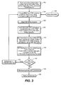
- FIG. 3 is a flow chart illustrating an operation of the system in FIG. 1 in writing data to the storage device where security configuration information is stored to illustrate one embodiment of the invention.
- FIG. 4 is a flow chart illustrating the operation of the system in FIG. 1 where the security configuration information stored is used to reconfigure the crypto-engine in retrying the write operation of the data that failed to be written previously, for illustrating an embodiment of the invention.
- the memory system 10 includes a central processing unit (CPU) 12 , a buffer management unit (BMU) 14 , a host interface module (HIM) 16 and a flash interface module (FIM) 18 , a flash memory 20 and a peripheral access module (PAM) 22 .
- Memory system 10 communicates with a host device 24 through a host interface bus 26 and port 26 a .
- the flash memory 20 which may be of the NAND type, provides data storage for the host device 24 .
- the software code for CPU 12 may also be stored in flash memory 20 .
- FIM 18 connects to the flash memory 20 through a flash interface bus 28 and port 28 a .
- HIM 16 is suitable for connection to a host system like a digital camera, personal computer, personal digital assistant (PDA), digital media player, MP-3 player, and cellular telephone or other digital devices.
- the peripheral access module 22 selects the appropriate controller module such as FIM, HIM and BMU for communication with the CPU 12 .
- all of the components of system 10 within the dotted line box may be enclosed in a single unit such as in memory card or stick 10 ′ and preferably encapsulated in the card or stick.
- the buffer management unit 14 includes a host direct memory access (HDMA) 32 , a flash direct memory access (FDMA) controller 34 , an arbiter 36 , a buffer random access memory (BRAM) 38 and a crypto-engine 40 .
- the arbiter 36 is a shared bus arbiter so that only one master or initiator (which can be HDMA 32 , FDMA 34 or CPU 12 ) can be active at any time and the slave or target is BRAM 38 .
- the arbiter is responsible for channeling the appropriate initiator request to the BRAM 38 .
- the HDMA 32 and FDMA 34 are responsible for data transported between the HIM 16 , FIM 18 and BRAM 38 or the CPU random access memory (CPU RAM) 12 a .
- the operation of the HDMA 32 and of the FDMA 34 is conventional and need not be described in detail herein.
- the BRAM 38 is used to buffer data passed between the host device 24 , flash memory 20 and CPU RAM 12 a .
- the HDMA 32 and FDMA 34 are responsible for transferring the data between HIM 16 /FIM 18 and BRAM 38 or the CPU RAM 12 a and for indicating sector transfer completion.
- unencrypted data When unencrypted data is sent by host device, through bus 26 , HIM 16 , HDMA 32 to the crypto-engine 40 , such unencrypted data may be stored in BRAM 38 . The data is then encrypted before it is sent to FDMA 34 on its way to memory 20 . Where the data written undergoes multistage cryptographic processing, preferably engine 40 completes such processing before the processed data is sent to memory 20 .
- the data stream is between the host device 24 and memory 20 .
- the data source is then host device 24 and the destination is memory 20 .
- the data source can also be the CPU 12 and the corresponding destination is the memory 20 in the writing operation. Whether the data source is host device 24 or CPU 12 , the data for storage in the flash memory 20 is first cryptographically processed by engine 40 before it is written to memory 20 .
- the memory system can in FIG. 1 contains a flash memory
- the system may alternatively contain another type of non-volatile memory instead, such as magnetic disks, optical CDs, as well as all other types of rewritable non-volatile memory systems, and the various advantages described below will equally apply to such alternative embodiments.
- the memory is also preferably encapsulated within the same physical body (such as a memory card or stick) along with the remaining components of the memory system.
- metapages When data stored in BRAM 38 (originating from either host device 24 or CPU 12 ) is written to flash memory 20 , the data is written in programmable units known as metapages, where a metapage is written to flash memory 20 during each programming cycle of the CPU 12 .
- One metapage may include a number of sectors, the size of the sector being defined by the host system. An example is a sector of 512 bytes of user data, following a standard established with magnetic disk drives, plus some number of bytes of overhead information about the user data and/or the metapage of which it is a part.
- the crypto-engine 40 performs the cryptographic process or processes using cryptographic algorithms and cryptographic keys. Many common cryptographic algorithms process 128 bits of data as a cryptographic processing unit. This is typically smaller than the size of metapages of data that are written during each programming cycle to flash memory 20 .
- each cryptographic processing unit which in this case consists of a cryptographic processing unit
- the resulting cipher text block of each cryptographic processing unit depends not only on the corresponding cryptographic processing unit, but also on the previous cryptographic processing units.
- FIG. 2 is a block diagram of a CBC process useful for illustrating the invention.
- the CBC process starts out with a random number called the initialization vector (IV).
- This number is encrypted by engine 40 using a key to arrive at a block of cipher text c 1 .
- the value c 1 and the first plain text block p 1 of the metapage are fed as inputs to an XOR gate, where the output of the gate is then encrypted again using a key to obtain cipher text c 2 .
- This operation is then repeated with c 2 and plain text block p 2 as inputs to a XOR gate where the output of the gate is encrypted by means of a key to obtain cipher text c 3 .
- the cipher text blocks are also referred to as message authentication codes (MAC) of the data stream.
- MAC message authentication codes
- Input m-bit key k; l-bit IV; l-bit plain text blocks p 1 , - - - p r .
- the values c 0 , . . . , c r above are the cipher text blocks or message authentication codes (MAC) of the metapage in the data stream, comprising plain text blocks p 1 , . . . , p r . IV is the initiation vector, and k is a key.
- MAC message authentication codes
- e k (x) means a process where x is encrypted by means of key k and e k ⁇ 1 (x) means x is decrypted using the key k.
- the entire encrypted Ith metapage, or c 0 , . . . , c r can be stored somewhere in system 10 , such as in a data buffer in memory 20 or RAM 12 a , so that when a problem is discovered in the writing process of the encrypted Ith metapage to flash memory 20 , the stored encrypted metapage can be fetched again and re-written to flash memory 20 . In this manner, the encrypted Ith metapage is not destroyed during the programming sequence so that it may be fetched later on in the event of a write failure.
- the programming code of CPU 12 includes a program command with no data transfer from the BRAM 38 . Instead, the program command would use the data buffer in a flash memory 20 or RAM 12 a as the data source and data is written again to the flash memory 20 . These programming modes can then be used when a write failure is discovered.
- Storing the encrypted metapage in a flash memory 20 or RAM 12 a would require the flash memory 20 or RAM 12 a to include a large size buffer adequate for storing the entire encrypted metapage.
- the unencrypted metapage may again be fetched from BRAM 38 and processed by engine 40 , and the processed metapage rewritten to memory 20 .
- context information or security configuration information of engine 40 is first stored in a buffer, such as in RAM 12 a of FIG. 1 .
- Such information preferably includes the last message authentication code or MAC value c r of the previous metapage, the various values of the registers of engine 40 , the cryptographic algorithm that is being used for the processing, and optionally information to identify the metapage (or its location) that needs to be rewritten, for reasons explained below.
- stored information preferably includes the initiation vector IV instead of the last message authentication code or MAC value of the previous metapage.
- the CPU 12 After storing such information, the CPU 12 returns control to the FIM and FDMA which process the current metapage i , cause it to be encrypted by engine 40 , and then write the encrypted current metapage to flash memory 20 .
- a buffer (not shown) between the FIM 18 and memory 20 to cache the encrypted metapage before it is written to flash memory 20 , such as one or more sectors of the metapage being processed.
- This buffer may also be part of the FIM 18 or memory 20 .
- the security configuration or context information stored preferably also includes the starting logical block addresses (LBAs) of the metapages that may be written to memory 20 at the same time, so that when it is discovered that the writing process of one of such metapages has failed, the system can be returned to the beginning address of such one metapage in order to rewrite it in encrypted form to flash memory 20 .
- LBAs logical block addresses
- the two buffers for storing the security configuration information may be labeled 12 a ( 0 ) and 12 a ( 1 ) and the bufferindex would toggle between 0 and 1 to point to one of the two buffers for storing security configuration information.
- the process for write fault recovery by means of storing the security configuration information is illustrated in FIG. 3 .
- the CPU 12 zeros out the context or security configuration information stored in the two buffers 12 a ( 0 ) and 12 a ( 1 ) and set the value of bufferindex to 0. (Block 102 .)
- the settings or context are loaded to the buffer management unit 14 and FIM 18 by CPU 12 . This sets up the FDMA 34 and causes FIM 18 to be ready to process data.
- the crypto-engine 40 is also configured. After such loading, CPU 12 waits until flash memory 20 is ready to receive data (Block 104 ). System 10 is then ready for write operation 106 .
- CPU 12 causes the FIM write program to start and transfers control of the various buses to FIM 18 .
- FIM 18 interrupts the CPU 12 just before transferring data from BRAM 38 to FIM 18 and flash memory 20 , that is, before issuing the DMA write operation code (Block 110 ).
- the back end (BE) Flash Ware and suspend/resume module (SRM) API are software read from a storage such as flash memory 20 to CPU RAM 12 a .
- the BE Flash Ware is executed by CPU 12 to invoke SRM API for saving crypto context or security configuration information of the metapage and of the engine 40 into the buffer that is pointed to by the value of the bufferindex.
- the BE Flash Ware executed by CPU 12 then returns control of the device 10 back to FIM 18 .
- the CPU 12 also causes the FDMA 34 to be started, so that data from BRAM 38 from the metapage is starting to be encrypted by crypto-engine 40 and written to memory 20 .
- the FIM 18 then checks to see whether the programming of the entire metapage to flash memory 20 is completed indicating that the programming of such metapage passes. (Diamond 116 ). If the metapage is successfully written to flash memory 20 without incident, the bufferindex is incremented by one and then divided by two (or modulo 2) to obtain the remainder.
- Block 122 In this instance where the bufferindex has been set to 0, such operation causes bufferindex to be 1 in block 122 and FIM 18 returns control to the CPU 12 in Block 104 to repeat the process for the next metapage. In the next cycle for writing the next metapage, the context or security configuration information will be written to buffer 12 a ( 1 ) instead, since the bufferindex has been set to 1.
- the FIM 18 then interrupts the processor 12 (Block 118 ) and the write operation is re-tried using a retry mechanism 120 .
- the retry mechanism is illustrated in FIG. 4 .
- the FIM 18 when FIM 18 discovers a failure of the write operation, the FIM 18 is aware of the location of the write failure and in which metapage the write failure occurred. FIM 18 is therefore aware of the beginning logical block address (LBA) of the metapage in which the write failure occurred.
- LBA logical block address
- This address is then matched with or compared to the starting LBA address in the two buffers 12 a ( 0 ) and 12 a ( 1 ) and identifies the buffer that contains the LBA address that matches that of the metapage at which the write failure occurred.
- Block 152 The context or security configuration information stored in such buffer that has been identified is then used to restore the state of the crypto-engine 40 .
- Block 154 The CPU 12 then activates FIM 18 , FDMA 34 , and engine 40 to again encrypt the metapage from BRAM 38 starting at the beginning logical block address of the metapage at which the write failure occurred and write the encrypted metapage to flash memory 20 as before.
- the FIM 18 also deletes or marks for deletion whatever incomplete encrypted metapage(s) that may have been written to memory 20 . After this operation has been completed, CPU 12 returns the operation to Block 104 of FIG. 3 .
- the CPU 12 will determine how far back the rewriting or reprogramming of data should go. In other words, the CPU 12 will determine whether to rewrite or reprogram just the metapage at which the write failure occurred, or whether to rewrite or reprogram also the metapage(s) preceding it as well.
- the preceding metapage(s) are also rewritten or reprogrammed if they have not been completely written to memory 20 even though no write failure occurred during their programming.
- the status of the programming of a particular metapage is known only after the next cached metapage finishes programming. In such event, CPU 12 will always go back two metapages (i.e. the metapage in which the write error occurred and the preceding one) for reprogramming, except that for the last metapage, it will only reprogram the last metapage.
Abstract
Description
Input: m-bit key k; l-bit IV; l-bit plain text blocks p1, - - - pr.
Output: c0, - - - , cr such that c0←IV and c i ←e k(c i-1 ⊕p i) for 1≦i≦r.
Decryption.
Input: m bit key k; l-bit IV; l-bit cipher text blocks c1, - - - cr.
Output: p0, - - - , pr such that p0←IV and p i ←c i-1 ⊕e k −1(c i) for 1≦i≦r.
Claims (28)
Priority Applications (5)
| Application Number | Priority Date | Filing Date | Title |
|---|---|---|---|
| US11/397,416 US7835518B2 (en) | 2006-04-03 | 2006-04-03 | System and method for write failure recovery |
| JP2009504395A JP2009537026A (en) | 2006-04-03 | 2007-03-30 | System and method for write failure recovery |
| PCT/US2007/065679 WO2007118034A2 (en) | 2006-04-03 | 2007-03-30 | System and method for write failure recovery |
| KR1020087024279A KR20080108119A (en) | 2006-04-03 | 2007-03-30 | System and method for write failure recovery |
| TW096111847A TW200817993A (en) | 2006-04-03 | 2007-04-03 | System and method for write failure recovery |
Applications Claiming Priority (1)
| Application Number | Priority Date | Filing Date | Title |
|---|---|---|---|
| US11/397,416 US7835518B2 (en) | 2006-04-03 | 2006-04-03 | System and method for write failure recovery |
Publications (2)
| Publication Number | Publication Date |
|---|---|
| US20070230691A1 US20070230691A1 (en) | 2007-10-04 |
| US7835518B2 true US7835518B2 (en) | 2010-11-16 |
Family
ID=38558935
Family Applications (1)
| Application Number | Title | Priority Date | Filing Date |
|---|---|---|---|
| US11/397,416 Active 2029-08-09 US7835518B2 (en) | 2006-04-03 | 2006-04-03 | System and method for write failure recovery |
Country Status (1)
| Country | Link |
|---|---|
| US (1) | US7835518B2 (en) |
Cited By (1)
| Publication number | Priority date | Publication date | Assignee | Title |
|---|---|---|---|---|
| US9489540B2 (en) | 2012-05-04 | 2016-11-08 | Samsung Electronics Co., Ltd. | Memory controller with encryption and decryption engine |
Families Citing this family (9)
| Publication number | Priority date | Publication date | Assignee | Title |
|---|---|---|---|---|
| US20070230690A1 (en) * | 2006-04-03 | 2007-10-04 | Reuven Elhamias | System for write failure recovery |
| US8634549B2 (en) * | 2008-05-07 | 2014-01-21 | Red Hat, Inc. | Ciphertext key chaining |
| US8396209B2 (en) | 2008-05-23 | 2013-03-12 | Red Hat, Inc. | Mechanism for chained output feedback encryption |
| US9087540B1 (en) | 2014-07-18 | 2015-07-21 | Seagate Technology Llc | Asymmetrical write fault thresholds |
| US9495988B1 (en) | 2014-10-21 | 2016-11-15 | Seagate Technology Llc | Dependent write fault threshold |
| US9236073B1 (en) | 2014-10-21 | 2016-01-12 | Seagate Technology Llc | Write fault threshold for a set of tracks |
| CN104657288B (en) * | 2015-03-03 | 2017-11-10 | 山东华芯半导体有限公司 | A kind of reading/writing method of SPI FLASH encryption interfaces and encryption data |
| DE102016215915A1 (en) * | 2016-08-24 | 2018-03-01 | Siemens Aktiengesellschaft | Secure configuration of a device |
| GB201721608D0 (en) * | 2017-12-21 | 2018-02-07 | Nordic Semiconductor Asa | A hardware cipher engine |
Citations (25)
| Publication number | Priority date | Publication date | Assignee | Title |
|---|---|---|---|---|
| US5438575A (en) | 1992-11-16 | 1995-08-01 | Ampex Corporation | Data storage system with stale data detector and method of operation |
| US6065679A (en) * | 1996-09-06 | 2000-05-23 | Ivi Checkmate Inc. | Modular transaction terminal |
| US6158004A (en) | 1997-06-10 | 2000-12-05 | Mitsubishi Denki Kabushiki Kaisha | Information storage medium and security method thereof |
| EP1074906A1 (en) | 1999-08-05 | 2001-02-07 | Sony Corporation | Card-shaped semiconductor storage device and operation setting method of the same |
| US6295604B1 (en) * | 1998-05-26 | 2001-09-25 | Intel Corporation | Cryptographic packet processing unit |
| US20020071553A1 (en) | 2000-10-20 | 2002-06-13 | Taizo Shirai | Data storage device, data recording method, data playback method, and program providing medium |
| US20020174337A1 (en) | 2001-04-27 | 2002-11-21 | Tadahiro Aihara | Memory card with wireless communication function and data communication method |
| US20020188812A1 (en) | 2001-06-12 | 2002-12-12 | Akila Sadhasivan | Implementing a dual partition flash with suspend/resume capabilities |
| WO2002101976A1 (en) | 2001-06-13 | 2002-12-19 | Corrent Corporation | Security association data cache |
| US20030085289A1 (en) | 2001-11-08 | 2003-05-08 | Yoshio Kaneko | Memory card and contents distributing system and method |
| US20030196028A1 (en) | 1999-10-21 | 2003-10-16 | Takuji Maeda | Semiconductor memory card access apparatus, a computer-readable recording medium, an initialization method, and a semiconductor memory card |
| US6754765B1 (en) | 2001-05-14 | 2004-06-22 | Integrated Memory Logic, Inc. | Flash memory controller with updateable microcode |
| US6928599B2 (en) | 2001-12-05 | 2005-08-09 | Intel Corporation | Method and apparatus for decoding data |
| US20060015754A1 (en) | 2004-07-15 | 2006-01-19 | International Business Machines Corporation | E-fuses for storing security version data |
| US20060050564A1 (en) | 2004-09-08 | 2006-03-09 | Kabushiki Kaisha Toshiba | Non-volatile semiconductor memory device |
| US7036020B2 (en) | 2001-07-25 | 2006-04-25 | Antique Books, Inc | Methods and systems for promoting security in a computer system employing attached storage devices |
| US20060107047A1 (en) | 2004-11-12 | 2006-05-18 | Hagai Bar-El | Method, device, and system of securely storing data |
| US20060232826A1 (en) | 2005-04-13 | 2006-10-19 | Hagai Bar-El | Method, device, and system of selectively accessing data |
| US20060259790A1 (en) * | 2005-05-13 | 2006-11-16 | Nokia Corporation | Implementation of an integrity-protected secure storage |
| US20060262928A1 (en) | 2005-05-23 | 2006-11-23 | Hagai Bar-El | Method, device, and system of encrypting/decrypting data |
| US20060294236A1 (en) | 2005-06-22 | 2006-12-28 | Hagai Bar-El | System, device, and method of selectively operating a host connected to a token |
| US20060294513A1 (en) | 2005-06-22 | 2006-12-28 | Hagai Bar-El | System, device, and method of selectively allowing a host processor to access host-executable code |
| US7215771B1 (en) | 2000-06-30 | 2007-05-08 | Western Digital Ventures, Inc. | Secure disk drive comprising a secure drive key and a drive ID for implementing secure communication over a public network |
| US20070230690A1 (en) | 2006-04-03 | 2007-10-04 | Reuven Elhamias | System for write failure recovery |
| US7493656B2 (en) | 2005-06-02 | 2009-02-17 | Seagate Technology Llc | Drive security session manager |
-
2006
- 2006-04-03 US US11/397,416 patent/US7835518B2/en active Active
Patent Citations (29)
| Publication number | Priority date | Publication date | Assignee | Title |
|---|---|---|---|---|
| US5438575A (en) | 1992-11-16 | 1995-08-01 | Ampex Corporation | Data storage system with stale data detector and method of operation |
| US6065679A (en) * | 1996-09-06 | 2000-05-23 | Ivi Checkmate Inc. | Modular transaction terminal |
| US6158004A (en) | 1997-06-10 | 2000-12-05 | Mitsubishi Denki Kabushiki Kaisha | Information storage medium and security method thereof |
| US6295604B1 (en) * | 1998-05-26 | 2001-09-25 | Intel Corporation | Cryptographic packet processing unit |
| EP1074906A1 (en) | 1999-08-05 | 2001-02-07 | Sony Corporation | Card-shaped semiconductor storage device and operation setting method of the same |
| US6829676B2 (en) | 1999-10-21 | 2004-12-07 | Matsushita Electric Industrial Co., Ltd. | Semiconductor memory card access apparatus, a computer-readable recording medium, an initialization method, and a semiconductor memory card |
| US20030196028A1 (en) | 1999-10-21 | 2003-10-16 | Takuji Maeda | Semiconductor memory card access apparatus, a computer-readable recording medium, an initialization method, and a semiconductor memory card |
| US7215771B1 (en) | 2000-06-30 | 2007-05-08 | Western Digital Ventures, Inc. | Secure disk drive comprising a secure drive key and a drive ID for implementing secure communication over a public network |
| US20020071553A1 (en) | 2000-10-20 | 2002-06-13 | Taizo Shirai | Data storage device, data recording method, data playback method, and program providing medium |
| US20020174337A1 (en) | 2001-04-27 | 2002-11-21 | Tadahiro Aihara | Memory card with wireless communication function and data communication method |
| US6754765B1 (en) | 2001-05-14 | 2004-06-22 | Integrated Memory Logic, Inc. | Flash memory controller with updateable microcode |
| US20020188812A1 (en) | 2001-06-12 | 2002-12-12 | Akila Sadhasivan | Implementing a dual partition flash with suspend/resume capabilities |
| US7062616B2 (en) | 2001-06-12 | 2006-06-13 | Intel Corporation | Implementing a dual partition flash with suspend/resume capabilities |
| WO2002101976A1 (en) | 2001-06-13 | 2002-12-19 | Corrent Corporation | Security association data cache |
| US7426747B2 (en) | 2001-07-25 | 2008-09-16 | Antique Books, Inc. | Methods and systems for promoting security in a computer system employing attached storage devices |
| US7036020B2 (en) | 2001-07-25 | 2006-04-25 | Antique Books, Inc | Methods and systems for promoting security in a computer system employing attached storage devices |
| US20030085289A1 (en) | 2001-11-08 | 2003-05-08 | Yoshio Kaneko | Memory card and contents distributing system and method |
| US6832731B2 (en) | 2001-11-08 | 2004-12-21 | Kabushiki Kaisha Toshiba | Memory card and contents distributing system and method |
| US6928599B2 (en) | 2001-12-05 | 2005-08-09 | Intel Corporation | Method and apparatus for decoding data |
| US20060015754A1 (en) | 2004-07-15 | 2006-01-19 | International Business Machines Corporation | E-fuses for storing security version data |
| US20060050564A1 (en) | 2004-09-08 | 2006-03-09 | Kabushiki Kaisha Toshiba | Non-volatile semiconductor memory device |
| US20060107047A1 (en) | 2004-11-12 | 2006-05-18 | Hagai Bar-El | Method, device, and system of securely storing data |
| US20060232826A1 (en) | 2005-04-13 | 2006-10-19 | Hagai Bar-El | Method, device, and system of selectively accessing data |
| US20060259790A1 (en) * | 2005-05-13 | 2006-11-16 | Nokia Corporation | Implementation of an integrity-protected secure storage |
| US20060262928A1 (en) | 2005-05-23 | 2006-11-23 | Hagai Bar-El | Method, device, and system of encrypting/decrypting data |
| US7493656B2 (en) | 2005-06-02 | 2009-02-17 | Seagate Technology Llc | Drive security session manager |
| US20060294236A1 (en) | 2005-06-22 | 2006-12-28 | Hagai Bar-El | System, device, and method of selectively operating a host connected to a token |
| US20060294513A1 (en) | 2005-06-22 | 2006-12-28 | Hagai Bar-El | System, device, and method of selectively allowing a host processor to access host-executable code |
| US20070230690A1 (en) | 2006-04-03 | 2007-10-04 | Reuven Elhamias | System for write failure recovery |
Non-Patent Citations (2)
| Title |
|---|
| International Search Report and Written Opinion for PCT/US2007/065679, dated Jul. 6, 2009, 14 pages. |
| Office Action for U.S. Appl. No. 11/397,101, dated Jun. 4, 2009, 10 pages. |
Cited By (1)
| Publication number | Priority date | Publication date | Assignee | Title |
|---|---|---|---|---|
| US9489540B2 (en) | 2012-05-04 | 2016-11-08 | Samsung Electronics Co., Ltd. | Memory controller with encryption and decryption engine |
Also Published As
| Publication number | Publication date |
|---|---|
| US20070230691A1 (en) | 2007-10-04 |
Similar Documents
| Publication | Publication Date | Title |
|---|---|---|
| US7835518B2 (en) | System and method for write failure recovery | |
| KR101323746B1 (en) | Memory System with In-Stream Data Encryption/Decryption | |
| US9396136B2 (en) | Cascaded data encryption dependent on attributes of physical memory | |
| US8966284B2 (en) | Hardware driver integrity check of memory card controller firmware | |
| US8375225B1 (en) | Memory protection | |
| US11368313B2 (en) | Data storage devices and methods for encrypting a firmware file thereof | |
| JP2010509690A (en) | Method and system for ensuring security of storage device | |
| US20060239450A1 (en) | In stream data encryption / decryption and error correction method | |
| JP5118494B2 (en) | Memory system having in-stream data encryption / decryption function | |
| US8843768B2 (en) | Security-enabled storage controller | |
| US8983072B2 (en) | Portable data carrier featuring secure data processing | |
| US8396208B2 (en) | Memory system with in stream data encryption/decryption and error correction | |
| JP2008524969A5 (en) | ||
| JP2008524754A (en) | Memory system having in-stream data encryption / decryption and error correction functions | |
| CN107861892B (en) | Method and terminal for realizing data processing | |
| US20070230690A1 (en) | System for write failure recovery | |
| WO2007118034A2 (en) | System and method for write failure recovery | |
| US20240086336A1 (en) | Storage device deleting encryption key, method of operating the same, and method of operating electronic device including the same | |
| CN116382562A (en) | Electronic device and method for simulating nonvolatile memory | |
| TW202403773A (en) | Semiconductor device, and system and method for managing secure operations in the same |
Legal Events
| Date | Code | Title | Description |
|---|---|---|---|
| AS | Assignment |
Owner name: SANDISK CORPORATION, CALIFORNIA Free format text: ASSIGNMENT OF ASSIGNORS INTEREST;ASSIGNORS:ELHAMIAS, REUVEN;MANI, VIVEK VENKATRAMAN;COHEN, NIV;REEL/FRAME:017569/0260;SIGNING DATES FROM 20060328 TO 20060402 Owner name: SANDISK CORPORATION, CALIFORNIA Free format text: ASSIGNMENT OF ASSIGNORS INTEREST;ASSIGNORS:ELHAMIAS, REUVEN;MANI, VIVEK VENKATRAMAN;COHEN, NIV;SIGNING DATES FROM 20060328 TO 20060402;REEL/FRAME:017569/0260 |
|
| STCF | Information on status: patent grant |
Free format text: PATENTED CASE |
|
| AS | Assignment |
Owner name: SANDISK TECHNOLOGIES INC., TEXAS Free format text: ASSIGNMENT OF ASSIGNORS INTEREST;ASSIGNOR:SANDISK CORPORATION;REEL/FRAME:026368/0968 Effective date: 20110404 |
|
| FPAY | Fee payment |
Year of fee payment: 4 |
|
| AS | Assignment |
Owner name: SANDISK TECHNOLOGIES LLC, TEXAS Free format text: CHANGE OF NAME;ASSIGNOR:SANDISK TECHNOLOGIES INC;REEL/FRAME:038809/0472 Effective date: 20160516 |
|
| MAFP | Maintenance fee payment |
Free format text: PAYMENT OF MAINTENANCE FEE, 8TH YEAR, LARGE ENTITY (ORIGINAL EVENT CODE: M1552) Year of fee payment: 8 |
|
| MAFP | Maintenance fee payment |
Free format text: PAYMENT OF MAINTENANCE FEE, 12TH YEAR, LARGE ENTITY (ORIGINAL EVENT CODE: M1553); ENTITY STATUS OF PATENT OWNER: LARGE ENTITY Year of fee payment: 12 |