US7843719B2 - Magnetic shift register and data accessing method - Google Patents
Magnetic shift register and data accessing method Download PDFInfo
- Publication number
- US7843719B2 US7843719B2 US12/365,847 US36584709A US7843719B2 US 7843719 B2 US7843719 B2 US 7843719B2 US 36584709 A US36584709 A US 36584709A US 7843719 B2 US7843719 B2 US 7843719B2
- Authority
- US
- United States
- Prior art keywords
- memory
- magnetic
- data
- read
- burst data
- Prior art date
- Legal status (The legal status is an assumption and is not a legal conclusion. Google has not performed a legal analysis and makes no representation as to the accuracy of the status listed.)
- Expired - Fee Related, expires
Links
Images


Classifications
-
- G—PHYSICS
- G11—INFORMATION STORAGE
- G11C—STATIC STORES
- G11C19/00—Digital stores in which the information is moved stepwise, e.g. shift registers
- G11C19/02—Digital stores in which the information is moved stepwise, e.g. shift registers using magnetic elements
- G11C19/08—Digital stores in which the information is moved stepwise, e.g. shift registers using magnetic elements using thin films in plane structure
- G11C19/0808—Digital stores in which the information is moved stepwise, e.g. shift registers using magnetic elements using thin films in plane structure using magnetic domain propagation
- G11C19/0841—Digital stores in which the information is moved stepwise, e.g. shift registers using magnetic elements using thin films in plane structure using magnetic domain propagation using electric current
-
- G—PHYSICS
- G11—INFORMATION STORAGE
- G11C—STATIC STORES
- G11C11/00—Digital stores characterised by the use of particular electric or magnetic storage elements; Storage elements therefor
- G11C11/02—Digital stores characterised by the use of particular electric or magnetic storage elements; Storage elements therefor using magnetic elements
- G11C11/14—Digital stores characterised by the use of particular electric or magnetic storage elements; Storage elements therefor using magnetic elements using thin-film elements
Definitions
- the present invention relates to a magnetic shift register memory and an accessing method thereof.
- a magnetic random access memory has advantages of non-volatile, high density, high accessing speed and anti-radiation, etc., which can be used to substitute a conventional semiconductor memory and used for embedded memory applications.
- the conventional magnetic field writing MRAM device applies metal wires for conducting currents and inducing the magnetic field, so as to switch a free layer of the MRAM.
- a demagnetizing field effect is quickly increased, and a required write current is greatly increased, so that miniaturization of the MRAM is difficult.
- a spin-torque-transfer (STT) switching technique is provided according to the MRAM technique, which is also referred to as a spin-RAM technique.
- STT spin-torque-transfer
- Such technique is a new generation of magnetic memory writing technique, by which the write current directly flows through a memory cell, and as a size of the memory cell decreases, the required write current accordingly decreases, so that such kind of memory can be perfectly miniaturized.
- STT switching technique still has disadvantages of inadequate thermal stability of devices, excessive write current, and uncertainty of reliability, etc., resulting in enormous obstacles for mass production of such kind of memory.
- U.S. Pat. No. 6,834,005B1 provides a device structure which can greatly improve a data storage capacity of a chip or a hard disk, and the device structure is referred to as a magnetic shift register memory.
- Such kind of memory has a chance to substitute a current dynamic random access memory (DRAM), a static random access memory (SRAM) and a flash chip, and can even implement a technique of “disk drive on a chip”.
- DRAM current dynamic random access memory
- SRAM static random access memory
- flash chip mainly applies a magnetic record disk similar to a hard disk, which is folded in a three-dimensional stack for storing data, in which the current drives a domain wall motion to record information therein. Therefore, an equivalent bit size thereof can be greatly reduced, and an operation speed thereof exceeds that of a solid flash chip and a hard disk.
- FIGS. 1A-1C are operational schematic diagrams of a conventional magnetic shift register.
- a shift register memory 100 includes a bit storage region 35 , a bit reservoir region 40 , a write device 15 and a read device 20 and a track 11 for storing and moving data.
- the track 11 of the shift register memory 100 is formed by a magnetic metal material such as ferromagnetic materials of NiFe, and CoFe, etc.
- the track 11 can be magnetized into a plurality of small magnetic domains 25 and 30 .
- Directions of magnetization vectors of the magnetic domains represent logic values 0 and 1 of the stored information.
- the track 11 of the shift register memory 100 is serially connected to adjacent tracks.
- a memory region is separated by one set of the write device 15 and the read device 20 , and each of the memory regions includes the bit storage region 35 and the bit reservoir region 40 .
- a quiescent state for storing information i.e., a stable state without the current being applied to drive a domain wall motion
- data of the memory cells for example, the magnetic domain 25 represents data 0 and the magnetic domain 30 represents data 1
- the bit storage region 35 is sequentially stored in the bit storage region 35 .
- none information is stored in the bit reservoir region 40 .
- the read device 20 of the magnetic shift register memory is connected to the track 11 via a magnetic tunnelling junction (MTJ), and when the sequential bit information is about to be read, a current pulse 45 is input to drive each of the magnetic domains 25 and 30 to generate a domain wall motion (DWM) towards a direction of the electron flow.
- MTJ magnetic tunnelling junction
- FIG. 1B illustrates a transient state, in which the bit information located closest to the read device 20 can be read.
- the transient state the previously read bit information is shifted into the bit reservoir region 40 .
- all of the bit information stored in the bit storage region 35 is read, all of the bit information is shifted to the bit reservoir region 40 .
- an inverted current pulse 45 is input to shift all of the bit information back to the bit storage region 35 .
- the magnetic domain to be written is also shifted to a position where the write device 15 is located by inputting the current pulse 45 , and now the write device 15 also shifts a stray field of a specific direction to a write position via another writing line according to the Ampere's field or DWM scheme, so that the magnetic domain is switched to a direction of the data to be written. Thereafter, the sequential information of the magnetic domain is shifted back to an original position via the inverted current pulse 45 .
- the read device 20 is connected to a sense amplifier through a select transistor (which can be a MOS transistor), wherein the transistor occupies a physical area of a Si substrate.
- Sizes of the magnetic domains 25 and 30 are generally far more smaller than that of the transistor, so that an equivalent bit size of the magnetic shift register memory is mainly determined by the size of the transistor and a number of the bit information ( 25 and 30 ) stored in the bit storage region 35 that is controlled by the transistor. Since the magnetic shift register memory includes a plurality of bits, the equivalent bit size can be greatly reduced.
- FIG. 2 is a schematic diagram illustrating a mechanism of the magnetic shift register of FIGS. 1A-1C .
- the shift register memory 100 can be extended on a straight track, which includes the bit storage region 35 and the bit reservoir region 40 respectively containing a plurality of the magnetic domains 25 and 30 .
- one bit storage region 35 of the shift register memory 100 records data of four bits that can be shifted to the bit reservoir region 40 .
- FIG. 3 is a schematic diagram illustrating a read mechanism. Referring to FIG.
- a current pulse 106 is, for example, input to the shift register memory 100 , so that the magnetic domains 102 and 104 are shifted, and a reading circuit 108 can read bit data from one of the magnetic domains passing through a position where the reading circuit 108 is located. Data to be written into the magnetic domain can be written by a writing circuit.
- design of the conventional magnetic shift register memory is still not ideal, and the magnetic shift register memory technique is still in an early stage of development, which requires further improvement.
- the memory cells are generally shifted for reading or writing data. After read or write of the data is completed, the memory cells are shifted back to original positions, so that a time for shifting the memory cells back to the original positions is wasted.
- FIG. 4 is a schematic diagram illustrating a mechanism of a conventional read operation.
- one clock cycle of a clock signal CLK is, for example, 10 ns.
- a position of the memory cell is, for example, determined according to an address signal Addr, and an address A 1 is activated at a time point 400 .
- a write enable signal WE represented by a compensation signal WE of WE is set to be disabled.
- An output enable signal (OE) represented by a compensation signal OE of OE is activated within one clock cycle after the address A 1 is activated. Meanwhile, after the output enable signal is activated, the domain walls are moved in response to a current pulse (WL pulse).
- the domain walls are sequentially moved forward for n positions to a buffer region during a time section 404 , and are sequentially moved backward for the n positions during a time section 406 to move the memory cells from the buffer region back to original positions thereof.
- a burst data to be read contains n bits data. Therefore, regarding a signal DIO on a data input/output pin (DIO pin), data reading is performed at the time point 402 , and a read operation is completed during a time section 410 . Next, another read operation is completed during a time section 414 .
- DIO pin data input/output pin
- one memory unit contains n-bit burst data, which is represented by (z).
- FIG. 5 is a schematic diagram illustrating a mechanism of a conventional write operation.
- the operation mechanism thereof is similar to that of FIG. 4 , in which waveforms of the write enable signal WE and the output enable signal OE are exchanged, and a write operation is completed during a time section 416 , while another write operation is further completed during a time section 418 .
- the domain walls are moved in response to the peripheral current pulse signal (WL pulse). For example, the domain walls are sequentially moved forward for n positions to the buffer region during a time section 420 , and are sequentially moved backward for the n positions during a time section 422 to move the memory cells from the buffer region back to the original positions.
- WL pulse peripheral current pulse
- the aforementioned conventional read and write operations all require the time section 406 or the time section 422 to move the memory cells back to the original addresses, so that an operation time thereof is increased, and an operation speed thereof is decreased.
- the present invention provides a magnetic shift register memory including at least one magnetic memory track, in which a plurality of domain walls separates the magnetic memory track into a plurality of magnetic domains to form a plurality of magnetic memory cells.
- a fixed number of the magnetic memory cells forms a memory unit to store a burst data.
- a read/write device is disposed between the memory units to read or write the burst data of the magnetic memory cells passing the read/write device.
- a flag unit records a flag value for each magnetic memory track or each memory unit to indicate whether the burst data is located at a first side or a second side of the read/write device.
- a current unit provides an operation current to the magnetic memory track according to the flag value to move the domain walls to pass the read/write device. After the read/write device reads or writes the burst data, the flag value is updated.
- the present invention provides a method for accessing a magnetic shift register memory.
- the magnetic shift register memory for example includes at least one magnetic memory track, in which a plurality of domain walls separates the magnetic memory track into a plurality of magnetic domains to form a plurality of magnetic memory cells.
- a fixed number of the magnetic memory cells forms a memory unit to store a burst data.
- a reading/write device is disposed between the memory units, and the magnetic memory track or each of the memory units has a corresponding flag value to indicate whether the burst data is located at a first side or a second side of the read/write device.
- the method includes following steps. First, the flag value of the magnetic memory track or the memory unit to be read/written is obtained. Next, an operation current is provided to the magnetic memory track to shift the domain walls to pass the read/write device according to the flag value. Finally, after the read/write device reads or writes the burst data of the passed magnetic memory cells, the flag value is updated.
- FIGS. 1A-1C are operational schematic diagrams of a conventional magnetic shift register memory.
- FIG. 2 is a schematic diagram illustrating a mechanism of a magnetic shift register of FIGS. 1A-1C .
- FIG. 3 is a schematic diagram illustrating a read mechanism.
- FIG. 4 is a schematic diagram illustrating a mechanism of a conventional read operation.
- FIG. 5 is a schematic diagram illustrating a mechanism of a conventional write operation.
- FIG. 7 is a schematic diagram illustrating a mechanism of a magnetic shift register memory with a high data transmission rate according to an embodiment of the present invention.
- FIG. 8 is a schematic diagram illustrating a memory chip which performs burst data inversing based on an external processing according to an embodiment of the present invention.
- FIG. 9 is a flowchart illustrating a read operation of an external processing according to an embodiment of the present invention.
- FIG. 10 is a flowchart illustrating a write operation of an external processing according to an embodiment of the present invention.
- FIG. 11 is a flowchart illustrating a read operation of an external processing according to an embodiment of the present invention.
- FIG. 12 is a flowchart illustrating a write operation of an external processing according to an embodiment of the present invention.
- FIG. 13 is a timing diagram of operation signals according to an embodiment of the present invention.
- FIG. 14 is a schematic diagram illustrating an internal processing memory chip according to an embodiment of the present invention.
- FIG. 15 is a flowchart illustrating a read/write operation of an internal processing according to an embodiment of the present invention.
- FIG. 16 is a flowchart illustrating a read operation of an internal processing according to an embodiment of the present invention.
- FIG. 17 is a flowchart illustrating a write operation of an internal processing according to an embodiment of the present invention.
- FIG. 18 is a timing diagram of read operation signals according to an embodiment of the present invention.
- FIG. 19 is a timing diagram of write operation signals according to an embodiment of the present invention.
- FIG. 20 is a schematic diagram illustrating a mechanism of a magnetic shift register memory according to an embodiment of the present invention.
- FIG. 21 is a schematic diagram illustrating a structure of a magnetic shift register memory according to an embodiment of the present invention.
- the present invention provides a magnetic shift register memory with a high data transmission rate, in which each word line or each memory unit has a flag signal recording whether a storage position of a corresponding burst data is located at one side or another side of a read/write device.
- a current source driving a domain wall motion (DWM) of a word line can determine a polarity of a current to be applied by checking a state of the flag signal.
- the magnetic shift register memory can have a double data transmission rate, and can input/output data according to a burst mode.
- the present invention provides a method for accessing the magnetic shift register memory, by which at least a time for moving back memory cells to original addresses in a conventional read and write mechanism is saved according to a flag setting mechanism, so as to improve an operation speed thereof.
- FIG. 6 is a schematic diagram illustrating an operation mechanism according to an embodiment of the present invention.
- the memory cells are not required to be shifted back to the original positions as that does in a conventional mechanism, so that waste of the operation time is avoided, and the operation speed can be improved.
- the read/write operation is activated at a time point 400 , after an initial latency, read data or written data is start to be transmitted though a data input/output pin DIO at a time point 402 .
- a read time section 500 and a write time section 502 can be interactively activated, freely, so as to perform a series of read/write operations.
- idle time sections existed in the conventional mechanism can be avoided. Namely, in the present invention, moving back the memory cells to fixed positions of the originally set addresses for each read or write operation is unnecessary.
- FIG. 7 is a schematic diagram illustrating a mechanism of a magnetic shift register memory with a high data transmission rate according to an embodiment of the present invention.
- the magnetic shift register memory includes at least a magnetic memory track, which is, for example, a magnetic nano line serving as a word line (WL).
- the magnetic nano lines used for data storage can be connected in series, and a driving current pulse for driving a DWM is provided from external.
- the magnetic nano lines are not necessarily to be connected in series.
- the word line for example, includes a plurality of memory units 700 - 706 .
- Multiple domain walls separate each of the magnetic memory units into a plurality of magnetic domains to form a plurality of magnetic memory cells, and 4 magnetic memory cells are taken as an example in FIG. 7 .
- a fixed number of the magnetic memory cells forms a memory unit to store a burst data, wherein the burst date includes n bits data.
- a read/write device 600 is disposed between the memory units to read or write the burst data of the magnetic memory cells passing the read/write device 600 .
- a flag unit records a flag value for each magnetic memory track or each memory unit to indicate whether the burst data is located at a first side or a second side of the read/write device 600 . For example, 0 or 1 of the flag value represents the two states.
- a current unit provides an operation current to the magnetic memory track (WL) according to the states of the flag value to move the domain walls to pass the read/write device 600 .
- the memory cells are, for example, moved rightwards (in terms of FIG. 7) for one memory unit, the memory unit 706 is moved out of a range of the figure, and a memory unit 708 of another side is moved into the range of the figure.
- the flag value traces and records positions of the memory units relative to the read/write device 600 . Due to tracing of the flag value, a state of FIG. 7( b ) can be maintained, and is unnecessary to be immediately recovered to the state of FIG. 7( a ).
- FIG. 7( c ) is obtained, by which the state of FIG. 7( a ) is recovered.
- the read/write operation can be simultaneously performed to change logical data of the memory cells.
- the corresponding flag value is directional.
- the bit accessed via the DWM is a first bit
- the bit accessed via the DWM is then a last bit. Therefore, input/output of the burst data has to be performed according to the state of the flag value to determine whether a sequence of the burst data is inversed, so as to avoid errors. Inversing of the sequence of the burst data can be implemented according to an internal or an external processing of the memory, which is described in detail in a following embodiment.
- a non-volatile memory such as a flash memory or a magnetic memory can be applied for storing the flag values.
- the stored flag value can be loaded to a memory with a relatively fast accessing speed, for example, a static random access memory (SRAM) latch or a SRAM register for operation.
- SRAM static random access memory
- the non-volatile memory is not applied for storing the flag values, but during a process of turning off the memory chip, all of the flag value signals are inspected, and all of the burst data are shifted back to original values thereof.
- the memory chip can be immediately utilized, and loading of the states of the flag value from the non-volatile memory is unnecessary.
- Such magnetic shift register memory can have a double data transmission rate, and data can be input/output in a burst mode, so that an operation efficiency of a system thereof can be greatly improved.
- FIG. 8 is a schematic diagram illustrating a memory chip which performs the burst data inversing based on the external processing according to an embodiment of the present invention.
- a data system 740 includes a magnetic memory chip 750 of the present invention.
- the memory chip 750 selects and activates an address (x, y) of the memory unit to be read/written via an Addr pin 752 .
- a DIO pin 754 is used for transmitting or receiving data. Due to the external processing, a Flag pin 756 is used for outputting the flag values. Another pin 758 can be used for other utilizations.
- FIG. 9 is a flowchart illustrating a read operation of the external processing according to an embodiment of the present invention.
- n bits data is read via a system interface 802 connected to a system.
- the system (S) is connected to the system interface 802 .
- the address (x, y) of the burst data to be read is selected and activated.
- the memory chip 750 outputs the corresponding flag value Flag(y).
- FIG. 10 is a flowchart illustrating a write operation of the external processing according to an embodiment of the present invention.
- n bits data is written via a system interface 902 connected to a system.
- the system (S) is connected to the system interface 902 .
- the address (x, y) to be written with the burst data is selected and activated.
- the memory chip 750 outputs the corresponding flag value Flag(y).
- step 914 the system processes the data sequence according to the states of the flag value, and inputs the burst data to the DIO pin 754 to perform the write operation.
- FIG. 11 is a flowchart illustrating a read operation of the external processing according to an embodiment of the present invention. Referring to FIG. 11 , it is a more detailed flowchart of the read operation.
- the system (s) is connected to a system interface 1102 disposed in the chip to read n bits data.
- the system (S) is connected to the system interface 1102 .
- the address (x, y) of the burst data to be read is selected and activated.
- the flag value Flag(y) is checked and the corresponding flag value Flag(y) is output.
- the positive/negative direction of the DWM and the positive/negative direction of the current pulse can be determined according to different definitions, and the positive direction of the current pulse is the opposite direction of the electron flow and can also be defined the same to the positive direction of the DWM.
- step 1112 the data stored in the memory cell is read by sensing magnetoresistance of the memory cell via a device such as a sense amplifier (SA), etc., wherein the data has a sequence of Q_ 1 -Q_n, and is output according to such sequence.
- step 1114 the data stored in the memory cell is read by sensing the magnetoresistance of the memory cell, wherein the data has a sequence of Q_n-Q_ 1 , and is output according to such sequence. Since the data sequence is adjusted by the external processing, the output sequence of the data is maintained to Q_n-Q_ 1 .
- step 1116 regarding the read memory unit, a position thereof relative to the read device is changed, so that the flag value thereof is required to be updated.
- step 1118 the external system determines whether the output sequence of the data is inversed according to the flag value output based on the step 1106 .
- FIG. 12 is a flowchart illustrating a write operation of the external processing according to an embodiment of the present invention. Referring to FIG. 12 , it is a more detailed flowchart of the write operation.
- n bits (W n bites) data is written via a system interface 1202 connected to a system.
- the system (S) is connected to the system interface 1202 .
- the address (x, y) to be written with the burst data is selected and activated.
- the corresponding flag value Flag (y) is checked, and the memory chip 750 outputs the flag value Flag(y).
- step 1212 the system inputs the burst data having the corresponding sequence to the DIO pin.
- step 1218 the burst data D_ 1 -D_n are written, and continued with the step 1216 , in step 1220 , the burst data D_n-D_ 1 are written.
- step 1222 the burst data is moved from one side of the read/write device to the other side, so that the flag value Flag(y) is correspondingly updated.
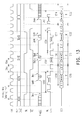
- FIG. 13 is a timing diagram of operation signals according to an embodiment of the present invention.
- the system for example, performs the write, read, write and read (W, R, W, R) operations in allusion to four addresses A 1 -A 4 .
- the flag value is first checked and the corresponding signal thereof is sent.
- the DIO data is started to be input or output, and after the read or write operation, the signal of Flag(y) is correspondingly updated to change the flag value.
- the burst data of D 1 _ 1 -D 1 — n are input to the DIO pin, and domain walls are moved in response to the current pulse (WL pulse), and accordingly the burst data is written into the memory cells by the write device, which is referred to as a write time section 1316 . Thereafter, a next burst data corresponds to the address A 2 .
- the burst data Q 2 — n -Q 2 _ 1 are read during a read time section 1318 .
- the current pulses are input during time sections 1304 and 1322 according to the states of the flag value Flag(y), so that the burst data D 3 — n -D 3 _ 1 are written during a time section 1320 , and the burst data Q 4 _ 1 -Q 4 — n are read during a time section 1322 .
- the data sequence is changed by the external system, so that if such mechanism is intended to be widely applied to current data systems, for example, computer systems, additional processing interfaces are required, or management of data accessing thereof is required to be changed.
- management of the data sequence can also be set to internal of the chip.
- FIG. 14 is a schematic diagram illustrating an internal processing memory chip according to an embodiment of the present invention.
- communication between the system 740 and the internal processing memory chip 750 only requires the address pin Addr. (x, y), the DIO pin and the other functional pin 758 . Since the data sequence is internally processed, the data transmitted by the memory chip 750 all have a predetermined sequence, so that the flag pin is not required.
- FIG. 15 is a flowchart illustrating a read/write operation of the internal processing according to an embodiment of the present invention.
- the system (S) is connected to a system interface 1502 to read n bits (R n bits) data.
- the address Addr (x, y) of the burst data to be read is selected and activated.
- the burst data Q_ 1 -Q_n are output, which are accorded to a general data sequence.
- the system directly obtains the data via the DIO pin. In other words, for the system, consideration of the states of the flag value is unnecessary.
- step 1518 the system (S) is connected to a system interface 1516 to write n bits (W n bits) data.
- step 1520 the address Addr (x, y) to be written with the burst data is selected and activated.
- step 1522 the system input the burst data D_ 1 -D_n to be written to the DIO pin. In other words, for the system, consideration of the states of the flag value is unnecessary.
- FIG. 16 is a flowchart illustrating a read operation of the internal processing according to an embodiment of the present invention.
- the system (S) is connected to a system interface 1602 disposed within the chip to read n bits data.
- the system (S) is connected to a system interface 1602 .
- the address (x, y) of the burst data to be read is selected and activated.
- the flag value Flag(y) is checked.
- step 1612 the data stored in the memory cell is read by sensing magnetoresistance of the memory cell via a device such as a sense amplifier (SA), etc., and the read data is latched, namely, such burst data is temporarily stored.
- SA sense amplifier
- step 1618 the state of the flag value is updated.
- step 1620 the output sequence of the data is maintained to Q_ 1 -Qn.
- step 1622 the system directly obtains the data, and consideration of the states of the flag value is unnecessary.
- FIG. 17 is a flowchart illustrating a write operation of the internal processing according to an embodiment of the present invention.
- n bits (W n bites) data is written via a system interface 1702 connected to the system.
- the system (S) is connected to the system interface 1702 .
- the address (x, y) to be written with the burst data is selected and activated.
- the corresponding flag value Flag (y) is checked.
- step 1708 the system inputs the burst data D_ 1 -D_n to the DIO pin, wherein the burst data D_ 1 -D_n is temporarily latched.
- step 1722 the state of the flag value is correspondingly updated after the write operation.
- FIG. 18 is a timing diagram of read operation signals according to an embodiment of the present invention.
- the sequence of the burst data is processed in the internal of the chip.
- the system for example, performs the read operation in allusion to a plurality of the addresses A 1 -A 4 .
- the read operation is determined according to the signals WE and OE .
- the flag value Flag(y) is first checked, and is updated after the read operation. Input of the operation current pulse (WL pulse) is performed according to the state of the flag value Flag(y).
- Data sensing and data latching are performed during a time section 1810 corresponding to the operation current pulse (WL pulse), and during a time section 1812 , whether the data sequence is inversed is determined according to the flag value.
- a first amount of the burst data is read at a time point 1802 after the time point 1800 , and then the burst data is consecutively read without recovering the memory cells to the original positions, and the output sequence of the burst data is maintained to the conventional sequence.
- FIG. 19 is a timing diagram of write operation signals according to an embodiment of the present invention.
- the sequence of the burst data is processed in the internal of the chip.
- the system for example, performs the write operation in allusion to a plurality of the addresses A 1 -A 4 .
- the write operation is determined according to the signals WE and OE .
- the flag value Flag(y) is first checked, and is updated after the write operation. Input of the operation current pulse (WL pulse) is performed according to the state of the flag value Flag(y).
- the sequence of the input data is inversed according to the flag value during a time section 1910 corresponding to the operation current pulse (WL pulse).
- the current pulse is input during a time section 1912 .
- the DIO pin inputs the burst data D 1 _ 1 -D 1 — n, D 2 _ 1 -D 2 — n, D 3 _ 1 -D 3 — n , . . . , etc.
- the first amount of the burst data can be input at a time point 1902 , and after the time section 1910 , the write operation is performed.
- FIG. 20 is a schematic diagram illustrating a mechanism of a magnetic shift register memory according to an embodiment of the present invention.
- the magnetic shift register memory 2200 includes at least one magnetic memory track.
- one magnetic memory track is taken as an example, on which a plurality of the domain walls separates the magnetic memory track into a plurality of magnetic memory cells 2250 and 2300 , wherein the domain walls are implemented by notches. By such means, a plurality of adjacent data regions is plotted in the memory cells.
- two data regions 2500 and 2502 are taken as an example, which are respectively formed by a fixed number of the magnetic memory cells to respectively store data of multiple bits.
- the data of four bits is taken as an example.
- One bit data in the magnetic memory cell is, for example, recorded by a direction of a magnetization vector.
- the data in the memory cells on the magnetic memory track can be shifted between the two adjacent data regions 2500 and 2502 under an operation current.
- Each of the data regions 2500 and 2502 for example, includes a read position (R) and a write position (W) to access the data of the magnetic domain shifted to the corresponding position.
- the read position (R) and the write position (W) can be disposed at an edge position of the data region.
- the read position (R) and the write position (W) can be located at the same position.
- the data region 2500 is a memory unit, in which application of a buffer region as that shown in FIG. 1A-1C is unnecessary.
- FIG. 21 is a schematic diagram illustrating a structure of a magnetic shift register memory according to an embodiment of the present invention.
- the magnetic shift register memory of the present embodiment includes a plurality of magnetic memory tracks disposed in parallel.
- Each of the magnetic memory tracks 3800 includes a plurality of magnetic memory cells separated by a plurality of the domain walls, which are shown as arrows of the magnetization vectors.
- a data region 3804 on each of the magnetic memory track 3800 is formed by a fixed number of the magnetic memory cells, and is used for storing data of multiple bits.
- the magnetic memory track 3800 can be briefly referred to as a track 3800 .
- a current driving unit 3802 applies an operation current to the selected magnetic memory track 3800 through write lines WL 0 , WL 1 , . . . , etc., so as to shift the magnetic memory cells of the data region 3804 to an adjacent data region.
- a read circuit unit includes a read circuit containing devices 3812 and 3810 , and has a read position at each of the data regions for reading a bit data of a magnetic memory cell passing through the read position within the selected data region.
- a writing circuit unit includes a device 3806 , and has a write position at each of the data regions for writing a bit data into a magnetic memory cell passing through the write position within the selected data region.
- the data region 3804 is located at one side (for example, the left side) of the read device 3810 and the write device 3806 according to the flag value. After the read/write operation is performed to the data region 3804 , the data region 3804 is shifted to the other side (for example, the right side) of the read device 3810 and the write device 3806 , and the flag value is correspondingly updated. Therefore, the data region 3804 shifted to the right side is unnecessary to be shifted back to the original left side, so that an operation speed thereof is increased.
Abstract
Description
Claims (16)
Applications Claiming Priority (3)
| Application Number | Priority Date | Filing Date | Title |
|---|---|---|---|
| TW97143755A | 2008-11-12 | ||
| TW97143755 | 2008-11-12 | ||
| TW097143755A TWI338898B (en) | 2008-11-12 | 2008-11-12 | Magetic shift register and data accessing method |
Publications (2)
| Publication Number | Publication Date |
|---|---|
| US20100118583A1 US20100118583A1 (en) | 2010-05-13 |
| US7843719B2 true US7843719B2 (en) | 2010-11-30 |
Family
ID=42165062
Family Applications (1)
| Application Number | Title | Priority Date | Filing Date |
|---|---|---|---|
| US12/365,847 Expired - Fee Related US7843719B2 (en) | 2008-11-12 | 2009-02-04 | Magnetic shift register and data accessing method |
Country Status (2)
| Country | Link |
|---|---|
| US (1) | US7843719B2 (en) |
| TW (1) | TWI338898B (en) |
Cited By (4)
| Publication number | Priority date | Publication date | Assignee | Title |
|---|---|---|---|---|
| US20100284216A1 (en) * | 2009-05-08 | 2010-11-11 | Samsung Electronics Co., Ltd. | Information storage devices using magnetic domain wall movement and methods of operating the same |
| US8750013B1 (en) | 2013-01-04 | 2014-06-10 | International Business Machines Corporation | Racetrack memory with low-power write |
| US9123421B2 (en) | 2013-01-21 | 2015-09-01 | International Business Machines Corporation | Racetrack memory cells with a vertical nanowire storage element |
| US10658063B2 (en) | 2017-10-26 | 2020-05-19 | Toshiba Memory Corporation | Semiconductor memory device including a correcting circuit |
Families Citing this family (5)
| Publication number | Priority date | Publication date | Assignee | Title |
|---|---|---|---|---|
| FR2879349B1 (en) * | 2004-12-15 | 2007-05-11 | Thales Sa | SPIN ELECTRONIC DEVICE HAVING A POLARIZED SPIN BEARER CURVED ARM DISPLACEMENT CONTROL |
| EP2671229B1 (en) | 2011-01-31 | 2019-10-09 | Everspin Technologies, Inc. | Method of writing to a spin torque magnetic random access memory |
| US8638601B1 (en) | 2012-07-06 | 2014-01-28 | International Business Machines Corporation | Domain wall motion in perpendicularly magnetized wires having magnetic multilayers with engineered interfaces |
| US8687415B2 (en) | 2012-07-06 | 2014-04-01 | International Business Machines Corporation | Domain wall motion in perpendicularly magnetized wires having artificial antiferromagnetically coupled multilayers with engineered interfaces |
| JP2020155178A (en) * | 2019-03-20 | 2020-09-24 | キオクシア株式会社 | Magnetic storage device |
Citations (5)
| Publication number | Priority date | Publication date | Assignee | Title |
|---|---|---|---|---|
| US6205047B1 (en) * | 1998-08-10 | 2001-03-20 | Kyoto University | Data memory device having an exclusive-or function and method of reading data therefrom |
| US6834005B1 (en) | 2003-06-10 | 2004-12-21 | International Business Machines Corporation | Shiftable magnetic shift register and method of using the same |
| US6898132B2 (en) | 2003-06-10 | 2005-05-24 | International Business Machines Corporation | System and method for writing to a magnetic shift register |
| US6955926B2 (en) | 2004-02-25 | 2005-10-18 | International Business Machines Corporation | Method of fabricating data tracks for use in a magnetic shift register memory device |
| US20060002180A1 (en) * | 2004-06-30 | 2006-01-05 | Stmicroelectronics, Inc. | Random access memory array with parity bit structure |
-
2008
- 2008-11-12 TW TW097143755A patent/TWI338898B/en not_active IP Right Cessation
-
2009
- 2009-02-04 US US12/365,847 patent/US7843719B2/en not_active Expired - Fee Related
Patent Citations (5)
| Publication number | Priority date | Publication date | Assignee | Title |
|---|---|---|---|---|
| US6205047B1 (en) * | 1998-08-10 | 2001-03-20 | Kyoto University | Data memory device having an exclusive-or function and method of reading data therefrom |
| US6834005B1 (en) | 2003-06-10 | 2004-12-21 | International Business Machines Corporation | Shiftable magnetic shift register and method of using the same |
| US6898132B2 (en) | 2003-06-10 | 2005-05-24 | International Business Machines Corporation | System and method for writing to a magnetic shift register |
| US6955926B2 (en) | 2004-02-25 | 2005-10-18 | International Business Machines Corporation | Method of fabricating data tracks for use in a magnetic shift register memory device |
| US20060002180A1 (en) * | 2004-06-30 | 2006-01-05 | Stmicroelectronics, Inc. | Random access memory array with parity bit structure |
Non-Patent Citations (2)
| Title |
|---|
| Article Titled "A novel SPRAM (SPin-transfer torque RAM) with a synthetic ferrimagnetic free layer for higher immunity to read disturbance and reducing write-current dispersion" jointly authored by Miura et al., in VLSI symposium, 2007, pp. 234-235. |
| Article Titled "Oscillatory dependence of current-driven magnetic domain wall motion on current pulse length" jointly authored by Thomas et al., in Nature, 443, pp. 197-200, 2006. |
Cited By (7)
| Publication number | Priority date | Publication date | Assignee | Title |
|---|---|---|---|---|
| US20100284216A1 (en) * | 2009-05-08 | 2010-11-11 | Samsung Electronics Co., Ltd. | Information storage devices using magnetic domain wall movement and methods of operating the same |
| US8374052B2 (en) * | 2009-05-08 | 2013-02-12 | Samsung Electronics Co., Ltd. | Information storage devices using magnetic domain wall movement and methods of operating the same |
| US8750013B1 (en) | 2013-01-04 | 2014-06-10 | International Business Machines Corporation | Racetrack memory with low-power write |
| US8750012B1 (en) | 2013-01-04 | 2014-06-10 | International Business Machines Corporation | Racetrack memory with low-power write |
| US9123421B2 (en) | 2013-01-21 | 2015-09-01 | International Business Machines Corporation | Racetrack memory cells with a vertical nanowire storage element |
| US9165675B2 (en) | 2013-01-21 | 2015-10-20 | Globalfoundries Inc. | Racetrack memory cells with a vertical nanowire storage element |
| US10658063B2 (en) | 2017-10-26 | 2020-05-19 | Toshiba Memory Corporation | Semiconductor memory device including a correcting circuit |
Also Published As
| Publication number | Publication date |
|---|---|
| TWI338898B (en) | 2011-03-11 |
| US20100118583A1 (en) | 2010-05-13 |
| TW201019332A (en) | 2010-05-16 |
Similar Documents
| Publication | Publication Date | Title |
|---|---|---|
| US7843719B2 (en) | Magnetic shift register and data accessing method | |
| US7872896B2 (en) | Magnetic shift register and operation method thereof | |
| JP5643230B2 (en) | Bit line voltage control in spin injection torque magnetoresistive random access memory | |
| CN106169302B (en) | Memory device and electronic device including the memory device | |
| US7085174B2 (en) | Semiconductor memory device with current driver providing bi-directional current to data write line | |
| US8315090B2 (en) | Pseudo page mode memory architecture and method | |
| EP2972892B1 (en) | Mixed memory type hybrid cache | |
| US8953368B2 (en) | Magnetic memory device having bidirectional read scheme | |
| JP2004355671A (en) | Storage device with arithmetic function, and arithmetic operation and storage method | |
| US9257166B2 (en) | Current sense amplifying circuit in semiconductor memory device | |
| JP2011192345A (en) | Spin transfer torque mram, and method for writing the same and method for reading the same | |
| US20140140124A1 (en) | Resistive memory device having selective sensing operation and access control method thereof | |
| JP2013196740A (en) | Semiconductor memory device and method of driving the same | |
| US9324387B2 (en) | Semiconductor memory device with data path option function | |
| US20040047177A1 (en) | Magnetic random access memory | |
| JPH11306750A (en) | Magnetic-type semiconductor integrated storage | |
| US10311931B2 (en) | Semiconductor memory device | |
| TWI790497B (en) | semiconductor memory device | |
| KR101847890B1 (en) | Pseudo page mode memory architecture and method | |
| US7154775B2 (en) | Magnetic random access memory | |
| US8213210B2 (en) | Magnetic shift register and reading method | |
| JP6557488B2 (en) | Nonvolatile memory device, storage device including the same, writing method and reading method thereof | |
| TWI752841B (en) | Memory device, method of copying data therein and electronic device | |
| JP2001148189A (en) | Data write-in method | |
| CN101752003A (en) | Magnetic shift register memory and data access method |
Legal Events
| Date | Code | Title | Description |
|---|---|---|---|
| AS | Assignment |
Owner name: INDUSTRIAL TECHNOLOGY RESEARCH INSTITUTE,TAIWAN Free format text: ASSIGNMENT OF ASSIGNORS INTEREST;ASSIGNORS:HUNG, CHIEN-CHUNG;SHEN, KUEI-HUNG;REEL/FRAME:022238/0373 Effective date: 20090116 Owner name: INDUSTRIAL TECHNOLOGY RESEARCH INSTITUTE, TAIWAN Free format text: ASSIGNMENT OF ASSIGNORS INTEREST;ASSIGNORS:HUNG, CHIEN-CHUNG;SHEN, KUEI-HUNG;REEL/FRAME:022238/0373 Effective date: 20090116 |
|
| STCF | Information on status: patent grant |
Free format text: PATENTED CASE |
|
| FPAY | Fee payment |
Year of fee payment: 4 |
|
| MAFP | Maintenance fee payment |
Free format text: PAYMENT OF MAINTENANCE FEE, 8TH YEAR, LARGE ENTITY (ORIGINAL EVENT CODE: M1552) Year of fee payment: 8 |
|
| FEPP | Fee payment procedure |
Free format text: MAINTENANCE FEE REMINDER MAILED (ORIGINAL EVENT CODE: REM.); ENTITY STATUS OF PATENT OWNER: LARGE ENTITY |
|
| LAPS | Lapse for failure to pay maintenance fees |
Free format text: PATENT EXPIRED FOR FAILURE TO PAY MAINTENANCE FEES (ORIGINAL EVENT CODE: EXP.); ENTITY STATUS OF PATENT OWNER: LARGE ENTITY |
|
| STCH | Information on status: patent discontinuation |
Free format text: PATENT EXPIRED DUE TO NONPAYMENT OF MAINTENANCE FEES UNDER 37 CFR 1.362 |
|
| FP | Lapsed due to failure to pay maintenance fee |
Effective date: 20221130 |