US7855458B2 - Electronic component - Google Patents

Electronic component Download PDF

Info

Publication number
US7855458B2
US7855458B2 US11/585,877 US58587706A US7855458B2 US 7855458 B2 US7855458 B2 US 7855458B2 US 58587706 A US58587706 A US 58587706A US 7855458 B2 US7855458 B2 US 7855458B2
Authority
US
United States
Prior art keywords
layer
electrode layer
substrate
electronic component
electrode
Prior art date
Legal status (The legal status is an assumption and is not a legal conclusion. Google has not performed a legal analysis and makes no representation as to the accuracy of the status listed.)
Expired - Fee Related, expires
Application number
US11/585,877
Other versions
US20070158848A1 (en
Inventor
Tsuyoshi Matsumoto
Yoshihiro Mizuno
Xiaoyu Mi
Hisao Okuda
Satoshi Ueda
Current Assignee (The listed assignees may be inaccurate. Google has not performed a legal analysis and makes no representation or warranty as to the accuracy of the list.)
Fujitsu Ltd
Original Assignee
Fujitsu Ltd
Priority date (The priority date is an assumption and is not a legal conclusion. Google has not performed a legal analysis and makes no representation as to the accuracy of the date listed.)
Filing date
Publication date
Application filed by Fujitsu Ltd filed Critical Fujitsu Ltd
Assigned to FUJITSU LIMITED reassignment FUJITSU LIMITED ASSIGNMENT OF ASSIGNORS INTEREST (SEE DOCUMENT FOR DETAILS). Assignors: MATSUMOTO, TSUYOSHI, MI, XIAOYU, MIZUNO, YOSHIHIRO, OKUDA, HISAO, UEDA, SATOSHI
Publication of US20070158848A1 publication Critical patent/US20070158848A1/en
Application granted granted Critical
Publication of US7855458B2 publication Critical patent/US7855458B2/en
Expired - Fee Related legal-status Critical Current
Adjusted expiration legal-status Critical

Links

Images

Classifications

    • HELECTRICITY
    • H01ELECTRIC ELEMENTS
    • H01LSEMICONDUCTOR DEVICES NOT COVERED BY CLASS H10
    • H01L27/00Devices consisting of a plurality of semiconductor or other solid-state components formed in or on a common substrate
    • H01L27/02Devices consisting of a plurality of semiconductor or other solid-state components formed in or on a common substrate including semiconductor components specially adapted for rectifying, oscillating, amplifying or switching and having at least one potential-jump barrier or surface barrier; including integrated passive circuit elements with at least one potential-jump barrier or surface barrier
    • H01L27/04Devices consisting of a plurality of semiconductor or other solid-state components formed in or on a common substrate including semiconductor components specially adapted for rectifying, oscillating, amplifying or switching and having at least one potential-jump barrier or surface barrier; including integrated passive circuit elements with at least one potential-jump barrier or surface barrier the substrate being a semiconductor body
    • HELECTRICITY
    • H01ELECTRIC ELEMENTS
    • H01GCAPACITORS; CAPACITORS, RECTIFIERS, DETECTORS, SWITCHING DEVICES OR LIGHT-SENSITIVE DEVICES, OF THE ELECTROLYTIC TYPE
    • H01G4/00Fixed capacitors; Processes of their manufacture
    • H01G4/002Details
    • H01G4/005Electrodes
    • H01G4/008Selection of materials
    • HELECTRICITY
    • H01ELECTRIC ELEMENTS
    • H01GCAPACITORS; CAPACITORS, RECTIFIERS, DETECTORS, SWITCHING DEVICES OR LIGHT-SENSITIVE DEVICES, OF THE ELECTROLYTIC TYPE
    • H01G4/00Fixed capacitors; Processes of their manufacture
    • H01G4/002Details
    • H01G4/228Terminals
    • H01G4/232Terminals electrically connecting two or more layers of a stacked or rolled capacitor
    • HELECTRICITY
    • H01ELECTRIC ELEMENTS
    • H01GCAPACITORS; CAPACITORS, RECTIFIERS, DETECTORS, SWITCHING DEVICES OR LIGHT-SENSITIVE DEVICES, OF THE ELECTROLYTIC TYPE
    • H01G4/00Fixed capacitors; Processes of their manufacture
    • H01G4/33Thin- or thick-film capacitors 
    • HELECTRICITY
    • H01ELECTRIC ELEMENTS
    • H01LSEMICONDUCTOR DEVICES NOT COVERED BY CLASS H10
    • H01L24/00Arrangements for connecting or disconnecting semiconductor or solid-state bodies; Methods or apparatus related thereto
    • H01L24/01Means for bonding being attached to, or being formed on, the surface to be connected, e.g. chip-to-package, die-attach, "first-level" interconnects; Manufacturing methods related thereto
    • H01L24/18High density interconnect [HDI] connectors; Manufacturing methods related thereto
    • HELECTRICITY
    • H01ELECTRIC ELEMENTS
    • H01LSEMICONDUCTOR DEVICES NOT COVERED BY CLASS H10
    • H01L28/00Passive two-terminal components without a potential-jump or surface barrier for integrated circuits; Details thereof; Multistep manufacturing processes therefor
    • H01L28/10Inductors
    • HELECTRICITY
    • H01ELECTRIC ELEMENTS
    • H01LSEMICONDUCTOR DEVICES NOT COVERED BY CLASS H10
    • H01L28/00Passive two-terminal components without a potential-jump or surface barrier for integrated circuits; Details thereof; Multistep manufacturing processes therefor
    • H01L28/40Capacitors
    • H01L28/60Electrodes
    • H01L28/75Electrodes comprising two or more layers, e.g. comprising a barrier layer and a metal layer

Definitions

  • the present invention relates to an electronic component that includes a capacitor provided on a substrate, for example formed by semiconductor processing technology.
  • RF radio frequency
  • the input/output terminal of each device is generally provided with a passive component such as an inductor or a capacitor, and that acts as a phase shifter for controlling the phase of the signals.
  • a SAW filter is employed for use as a narrow-band frequency filter.
  • the SAW filter which includes a piezoelectric element, produces a difference in potential between piezoelectric element electrodes because of a piezoelectric effect, when a physical impact or a thermal effect is applied to the SAW filter or the piezoelectric element thereof during the manufacturing process of the apparatus in which the SAW filter is incorporated.
  • a predetermined voltage is applied to an electronic component electrically connected to the SAW filter.
  • the capacitor included in the passive element is usually electrically connected to the SAW filter, and hence the capacitor has to have a high withstand voltage (150 V or higher, for instance), to thereby prevent a dielectric breakdown between the capacitor electrodes, which may take place upon application of a voltage accidentally generated by the SAW filter or the piezoelectric element thereof.
  • an integrated passive device (hereinafter, IPD) manufactured based on a semiconductor processing technology, which includes a plurality of predetermined passive components such as an inductor, a capacitor, a resistance and a filter densely integrated on a substrate, may be employed as the passive element (phase shifter).
  • IPD integrated passive device
  • the capacitor included therein still has to have a high withstand voltage, for preventing a dielectric breakdown between the capacitor electrodes, as stated above.
  • Techniques related to the IPD are found, for example, in JP-A-H04-61264 and JP-A-2002-33239.
  • the capacitor included in the IPD generally has a laminate structure consisting of a lower electrode layer provided on a substrate, an upper electrode layer opposed to the lower electrode layer, and a dielectric layer disposed between the electrode layers.
  • the lower electrode layer and the upper electrode layer are both expected to have low resistance and to achieve sufficient adhesion to the dielectric layer. Insufficient adhesion between the layers provokes deterioration with time in adhesion status between those layers (for example, expansion of a gap between the layers with time), thus causing variation in static capacitance characteristic of the capacitor, which is undesirable.
  • the lower electrode layer of the capacitor included in the IPD is often constituted of a multilayer structure including Ti/Au/Ni/Au layers.
  • such multilayer structure includes a Ti layer (for instance, 50 nm in thickness) provided on a substrate, a first Au layer (for instance, 500 nm in thickness) provided on the Ti layer, a Ni layer (for instance, 50 nm in thickness) provided on the first Au layer, and a second Au layer (for instance, 500 nm in thickness) provided on the Ni layer, such that a minute amount of Ni originating from the Ni layer reaches the surface of the second Au layer on the side of the dielectric layer, because of thermal diffusion.
  • Such multilayer structure is known to have low resistance, and to achieve sufficient adhesion especially to a SiO 2 dielectric layer, because of the presence of Ni on the surface of the second Au layer on the side of the dielectric layer.
  • Employing the Ti/Au/Ni/Au multilayer structure as the lower electrode layer may not always assure the required adhesion performance between the lower electrode layer and the dielectric layer. Also, employing the Ti/Au/Ni/Au multilayer structure as the lower electrode layer may lead to failure in attaining the withstand voltage of a required level in the capacitor. Increasing the thickness of the dielectric layer may help in improving the withstand voltage of the capacitor, however the increase in thickness of the dielectric layer requires as much increase in area of the upper electrode layer, in order to secure the required static capacitance of the capacitor. Therefore, increasing the thickness of the dielectric layer is not a desirable solution, from the view point of suppressing an increase in dimensions of the capacitor, hence the IPD including the capacitor as a component.
  • the present invention has been proposed under the foregoing situation, with an object to provide an electronic component including a capacitor unit that assures sufficient adhesion between the lower electrode layer and the dielectric layer, and that facilitates achieving a high withstand voltage.
  • a first aspect of the present invention provides an electronic component comprising a substrate and a capacitor unit.
  • the capacitor unit has a laminate structure including a first electrode layer (lower electrode layer) provided on the substrate, a second electrode layer (upper electrode layer) opposed to the first electrode layer, and a dielectric layer disposed between the first and the second electrode layers.
  • the first electrode layer has a multilayer structure including an adhesion metal layer joined to the dielectric layer, via an oxide coating provided on a surface of the adhesion metal layer.
  • the adhesion metal layer according to the first aspect of the present invention a metal material oxidizable to such an extent as forming an oxide coating on a surface thereof in an atmosphere of a normal temperature and pressure is deposited, and then the growing facet of the metal layer is actually exposed to air for oxidation. Therefore, the adhesion metal layer according to the first aspect of the present invention is an easily oxidizable metal layer.
  • the electronic component according to the present invention includes the capacitor element itself, and an integrated electronic component in which the capacitor element is integrated with another element.
  • the present inventors discovered that the lower electrode layer joined to the dielectric layer via a surface coating constituted of an easily oxidizable metal provided on the surface of the lower electrode layer can achieve superior adhesion to the dielectric layer, than the conventional lower electrode layer having the Ti/Au/Ni/Au multilayer structure.
  • the present inventors also discovered that employing the lower electrode layer provided with such metal layer enables achieving a higher withstand voltage than employing the conventional lower electrode layer having the Ti/Au/Ni/Au multilayer structure.
  • the first aspect of the present invention is based on these findings.
  • the first electrode layer (lower electrode layer) is joined to the dielectric layer via the oxide coating provided on the adhesion metal layer of the first electrode layer.
  • the oxide coating has a metal oxide structure rooted in the metal foundation of the adhesion metal layer.
  • the oxide coating having such metal oxide structure is readily combinable to the dielectric layer, which is generally constituted of silicon oxide, silicon nitride, aluminum oxide, tantalum oxide, or titanium oxide. It is because of such high bonding performance between the oxide coating and the dielectric layer, that the first electrode layer achieves superior adhesion to the dielectric layer.
  • the effect of blocking the flow of electrons from the main portion of the first electrode layer to the dielectric layer, provided by the oxide coating having the metal oxide structure can be construed to be a reason of the high withstand voltage of the capacitor unit according to the present invention.
  • the adhesion metal layer may contain a metal selected from the group consisting of Ti, Cr, and Ta.
  • Ti, Cr, and Ta are so-called easily oxidizable metals, which are oxidized under a relatively mild condition in a normal atmosphere.
  • a second aspect of the present invention provides an electronic component comprising a substrate and a capacitor unit.
  • the capacitor unit has a laminate structure including a first electrode layer (lower electrode layer) provided on the substrate, a second electrode layer (upper electrode layer) opposed to the first electrode layer, and a dielectric layer disposed between the first and the second electrode layers.
  • the first electrode layer has a multilayer structure including an adhesion metal layer, containing a metal selected from the group consisting of Ti, Cr and Ta, and joined to the dielectric layer.
  • a metal material containing a metal selected from the group consisting of Ti, Cr and Ta is deposited, but without positively exposing the growing facet of the metal layer to air.
  • the second aspect of the present invention is, as stated above, based on the finding that the lower electrode layer joined to the dielectric layer via a surface coating constituted of an easily oxidizable metal provided on the surface of the lower electrode layer can achieve superior adhesion to the dielectric layer, than the conventional lower electrode layer having the Ti/Au/Ni/Au multilayer structure, and the finding that employing the lower electrode layer provided with such metal layer enables achieving a higher withstand voltage than employing the conventional lower electrode layer having the Ti/Au/Ni/Au multilayer structure.
  • the first electrode layer may include an adhesion layer, containing the metal contained in the adhesion metal layer and joined to the substrate.
  • an adhesion layer containing the metal contained in the adhesion metal layer and joined to the substrate.
  • Such structure allows improving the formation efficiency of the capacitor unit, and hence the production efficiency of the electronic component. This is because the structure enables, for example when performing a sputtering process with a plurality of targets to form the first electrode layer, simplifying the selection of the targets.
  • the first electrode layer may include a main conductive layer containing a metal selected from the group consisting of Cu, Au, Ag, and Al. Such structure is appropriate in reducing the resistance of the first electrode layer.
  • the electronic component according to the present invention may further comprise an interconnect layer provided on the substrate, and the interconnect layer may have a structure same as the multilayer structure of the first electrode layer, but without the adhesion metal layer. It is preferable that the interconnect layer and the first electrode layer constitute a continuous structure, except for the adhesion metal layer.
  • the electronic component according to the present invention may further comprise a passive component provided on the substrate, such that the interconnect layer constitutes at least a part of an electrical path between the passive component and the capacitor unit.
  • the electronic component according to the present invention may further comprise an electrode pad provided on the substrate, such that the interconnect layer constitutes at least a part of an electrical path between the electrode pad and the capacitor unit.
  • the electronic component according to the present invention may be an integrated electronic component including the foregoing structures.
  • FIG. 1 is a plan view showing an integrated electronic component according to the present invention
  • FIG. 2 is a cross-sectional view taken along the line II-II in FIG. 1 ;
  • FIG. 3 is a cross-sectional view taken along the line III-III in FIG. 1 ;
  • FIG. 4 is a circuit diagram of the integrated electronic component shown in FIG. 1 ;
  • FIG. 5 is a schematic diagram showing a laminate structure of a capacitor unit of the integrated electronic component shown in FIG. 1 ;
  • FIGS. 6( a ) to 6 ( d ) are cross-sectional views showing a manufacturing method of the integrated electronic component shown in FIG. 1 ;
  • FIGS. 7( a ) to 7 ( c ) are cross-sectional views showing the manufacturing method subsequent to FIG. 6( d );
  • FIGS. 8( a ) to 8 ( c ) are cross-sectional views showing the manufacturing method subsequent to FIG. 7( c ).
  • FIGS. 1 to 3 depict an integrated electronic component X according to the present invention.
  • FIG. 1 is a plan view of the integrated electronic component X.
  • FIGS. 2 and 3 are cross-sectional views taken along the line II-II and III-III in FIG. 1 , respectively.
  • the integrated electronic component X includes a substrate S, capacitors 10 A, 10 B, a coil inductor 20 , electrode pads 30 A, 30 B, 30 C, 30 D, an interconnect 40 , and a cover layer 50 (not shown in FIG. 1 ), and has a circuit configuration shown in FIG. 4 .
  • the substrate S may be a semiconductor substrate, a quartz substrate, a glass substrate, a silicon on insulator (SOI) substrate, a silicon on quartz (SOQ) substrate, or a silicon on glass (SOG) substrate.
  • the semiconductor substrate may be constituted of a silicon material, such as monocrystalline silicon.
  • the capacitors 10 A, 10 B respectively have a laminate structure including electrode layers 11 , 12 and a dielectric layer 13 .
  • the laminate structure of the capacitors 10 A, 10 B is shown in FIG. 5 .
  • the electrode layer 11 is a lower electrode layer formed in a pattern on the substrate S, and has a laminate structure including an underlying adhesion layer 11 a , a main conductive layer 11 b and an adhesion metal layer 11 c in this embodiment, as shown in FIGS. 2 and 5 .
  • the underlying adhesion layer 11 a serves to secure sufficient adhesion between the substrate S and the electrode layer 11 , and may preferably be constituted of Ti, Cr, or Ta.
  • the underlying adhesion layer 11 a has a thickness of, for instance, 30 to 100 nm.
  • the main conductive layer 11 b is the principal part of the electrode layer 11 , engaged in electrical conduction which is the primary purpose thereof, and may be constituted of Cu, Au, Ag, or Al.
  • the main conductive layer 11 b has a thickness of 0.5 to 2 ⁇ m, for instance.
  • the adhesion metal layer 11 c which serves to secure sufficient adhesion between the dielectric layer 13 and the electrode layer 11 , includes an oxide coating 11 c ′ formed on the surface of the adhesion metal layer 11 c confronting the dielectric layer 13 in this embodiment, as schematically shown in FIG. 5 .
  • the adhesion metal layer 11 c without the oxide coating 11 c ′ provided on the surface thereof confronting the dielectric layer 13 may be employed, instead of the adhesion metal layer 11 c provided with such oxide coating 11 c ′.
  • the base metal material constituting the adhesion metal layer 11 c include Ti, Cr, and Ta. These are so-called easily oxidizable metals, which are oxidized under a relatively mild condition in a normal atmosphere.
  • An overall thickness of the adhesion metal layer 11 c thus configured is, for instance, 30 to 100 nm.
  • the electrode layer 12 is an upper electrode layer formed so as to confront the electrode layer 11 via the dielectric layer 13 , and has a laminate structure including an underlying adhesion layer 12 a and a main conductive layer 12 b in this embodiment, as shown in FIG. 5 .
  • the underlying adhesion layer 12 a serves to secure sufficient adhesion between the dielectric layer 13 and the electrode layer 12 , and may be constituted of Ti, Cr, or Ta.
  • the underlying adhesion layer 12 a has a thickness of, for instance, 30 to 100 nm.
  • the main conductive layer 12 b is a principal part of the electrode layer 12 , engaged in electrical conduction which is the primary purpose thereof, and may be constituted of Cu, Au, Ag, or Al.
  • the main conductive layer 12 b may have a thickness of 1 to 15 ⁇ m.
  • the electrode layer 12 may have a single layer structure instead of such laminate structure.
  • the dielectric layer 13 may preferably be constituted of an oxide dielectric or a nitride dielectric, such as silicon oxide, silicon nitride, aluminum oxide, tantalum oxide, or titanium oxide.
  • the dielectric layer 13 may have a thickness of 0.1 to 1 ⁇ m.
  • the coil inductor 20 is a flat spiral coil patterned on the substrate S as shown in FIGS. 1 and 3 , and has end portions 21 , 22 .
  • Preferable materials of the coil inductor 20 include Cu, Au, Ag and Al.
  • the electrode pads 30 A to 30 D serve for external connection.
  • the electrode pads 30 A, 30 B serve as terminals for ground connection, while the electrode pads 30 C, 30 D serve as input/output terminals of electrical signals.
  • the electrode pads 30 A to 30 D may be constituted of a Ni body with the upper surface coated with a Au layer.
  • the interconnect 40 serves to electrically connect the components on the substrate S, and includes a first interconnect region 41 patterned on the substrate S, a second interconnect region 42 patterned mainly on the cover layer 50 , and a third interconnect region 43 connecting the first interconnect region 41 and the second interconnect region 42 , as shown in FIGS. 1 to 3 .
  • first interconnect region 41 among the interconnects is indicated by hatching in FIG. 1 .
  • the first interconnect region 41 has a structure same as the multilayer structure of the electrode layer 11 of the capacitor units 10 A, 10 B, but without the adhesion metal layer 11 c .
  • the first interconnect region 41 includes an underlying adhesion layer of the same composition and thickness as those of the underlying adhesion layer 11 a , and a main conductive layer of the same composition and thickness as those of the main conductive layer 11 b .
  • a portion of the first interconnect region 41 constitutes the electrode layer 11 .
  • Preferable materials of the second interconnect region 42 and the third interconnect region 43 include Cu, Au, Ag, and Al.
  • the second interconnect region 42 may have a thickness of 1 to 15 ⁇ m.
  • the capacitor 10 A is electrically connected to the electrode pads 30 A, 30 C and the coil inductor 20 . More specifically, the electrode layer 11 of the capacitor 10 A is electrically connected to the electrode pad 30 A, and the electrode layer 12 of the capacitor 10 A to the electrode pad 30 C and the end portion 21 of the coil inductor 20 .
  • the capacitor 10 B is electrically connected to the electrode pads 30 B, 30 D and the coil inductor 20 . More specifically, the electrode layer 11 of the capacitor 10 B is electrically connected to the electrode pad 30 B, and the electrode layer 12 of the capacitor 10 B to the electrode pad 30 D and the other end portion 22 of the coil inductor 20 .
  • the cover layer 50 may be constituted of a polyimide or benzocyclobutene (BCB), and covers the capacitors 10 A, 10 B, the coil inductor 20 , the first interconnect region 41 , and the third interconnect region 43 .
  • BCB benzocyclobutene
  • FIGS. 6( a ) to 8 ( c ) illustrate a manufacturing method of the integrated electronic component X.
  • FIGS. 6( a ) to 8 ( c ) represent the progress of the formation process of a capacitor 10 (corresponding to the capacitor 10 A, 10 B), a part of the coil inductor 20 , an electrode pad 30 (corresponding to the electrode pads 30 A to 30 D), and a part of an interconnect 40 shown in FIG. 8( c ), in cross-sectional views of a region including these constituents.
  • the cross-sectional views progressively depict a model of a plurality of predetermined regions included in a single section where the integrated electronic component is formed, on a material substrate to be processed.
  • an underlying layer 61 , a main conductive layer 62 , and a metal layer 63 with an oxide coating (not shown) provided on the surface thereof are consecutively formed on the substrate S as shown in FIG. 6( a ), for example by a sputtering process.
  • the underlying layer 61 , the main conductive layer 62 , and the metal layer 63 are respectively constituted of the materials cited regarding the underlying adhesion layer 11 a , the main conductive layer 11 b , and the adhesion metal layer 11 c of the electrode layer 11 of the capacitor 10 .
  • the metal layer 63 with the oxide coating may be formed by depositing an easily oxidizable metal such as Ti, Cr, or Ta on the main conductive layer 62 , and exposing that metal to air.
  • an easily oxidizable metal such as Ti, Cr, or Ta
  • the easily oxidizable metal is not exposed to air after being deposited on the main conductive layer 62 , when forming the metal layer 63 .
  • a resist pattern 64 is formed, as shown in FIG. 6( b ).
  • the resist pattern 64 has a pattern shape corresponding to the electrode layer 11 and the first interconnect region 41 of the capacitor 10 .
  • a liquid photoresist is firstly deposited on the metal layer 63 by a spin coating process.
  • the photoresist layer is then patterned through an exposure and a subsequent development process.
  • the resist pattern and the cover layer to be described later may also be formed through a similar process.
  • an ion milling process is performed utilizing the resist pattern 64 as the mask, so as to etch on the underlying layer 61 , the main conductive layer 62 , and the metal layer 63 .
  • a predetermined stripping solution is then applied to remove the resist pattern 64 .
  • the dielectric layer 65 is constituted of one of the materials cited regarding the dielectric layer 13 of the capacitor 10 .
  • a resist pattern 66 is formed on the dielectric layer 65 .
  • the resist pattern 66 has a pattern shape corresponding to the dielectric layer 13 of the capacitor 10 .
  • a wet etching process is then performed on the dielectric layer 65 utilizing the resist pattern 66 as the mask, as shown in FIG. 7( b ). As a result, the dielectric layer 13 is shaped in a predetermined pattern. Suitable etching solutions for such wet etching process include buffered fluoric acid.
  • an exposed portion of the metal layer 63 is removed as shown in FIG. 7( c ), by an etching process utilizing the resist pattern 66 and the dielectric layer 13 as the mask.
  • the electrode layer 11 and the first interconnect region 41 of the capacitor 10 are patterned. Suitable etching processes include an ion milling process and a wet etching process. Upon completing this process, the resist pattern 66 is removed.
  • an electroplating process is performed with a predetermined resist pattern (not shown), so as to grow a conductive material at predetermined positions.
  • a predetermined resist pattern not shown
  • the cover layer 50 is then formed as shown in FIG. 8 b ).
  • the cover layer 50 is formed with openings 51 , 52 , 53 , through which a portion of the electrode layer 12 , a portion of the first interconnect region 41 , and a portion of the main part of the electrode pad 30 , respectively.
  • an electroplating process is performed with a predetermined resist pattern (not shown), so as to grow a conductive material at predetermined positions.
  • a predetermined resist pattern not shown
  • the second interconnect region 42 , the third interconnect region 43 , and the surface layer of the electrode pad 30 are formed.
  • the integrated electronic component X shown in FIG. 1 can be manufactured.
  • the present invention is, as already stated, based on the finding that the lower electrode layer joined to the dielectric layer via a surface coating constituted of an easily oxidizable metal provided on the surface of the lower electrode layer can achieve superior adhesion to the dielectric layer, than the conventional lower electrode layer having the Ti/Au/Ni/Au multilayer structure, as well as on the finding that employing the lower electrode layer provided with such metal layer enables achieving a higher withstand voltage than employing the conventional lower electrode layer having the Ti/Au/Ni/Au multilayer structure, the electrode layer 11 (lower electrode layer) of the capacitor units 10 A, 10 B in the integrated electronic component X is joined to the dielectric layer 13 via the oxide coating 11 c ′ (shown in FIG.
  • the oxide coating 11 c ′ has a metal oxide structure rooted in the metal foundation of the adhesion metal layer 11 c .
  • the oxide coating 11 c ′ having such metal oxide structure is readily combinable to the dielectric layer 13 (constituted of silicon oxide, silicon nitride, aluminum oxide, tantalum oxide, titanium oxide or the like). Accordingly, the electrode layer 11 can achieve excellent adhesion to the dielectric layer 13 .
  • the oxide coating 11 c ′ having the metal oxide structure blocks the flow of electrons from the metal foundation of the main conductive layer 11 b and the adhesion metal layer 11 c in the electrode layer 11 to the dielectric layer 13 , thus granting a high withstand voltage to the capacitors 10 A, 10 B.
  • the capacitors 10 A, 10 B of the integrated electronic component X can achieve excellent adhesion between the electrode layer 11 (lower electrode layer) and the dielectric layer 13 , as well as a high withstand voltage.
  • a plurality of capacitor elements was fabricated according to the present invention.
  • capacitor units having a laminate structure configured as FIG. 5 under the following conditions, were made on a glass substrate.
  • the underlying adhesion layer 11 a of the electrode layer 11 was a Ti layer of 50 nm in thickness.
  • the main conductive layer 11 b was a Au layer of 1000 nm in thickness.
  • the adhesion metal layer 11 c was a Ti layer of 50 nm in thickness, including an oxide coating on its surface.
  • the electrode layer 12 was an electroplated Cu layer of 10 ⁇ m in thickness.
  • the dielectric layer 13 was a SiO 2 layer of 220 nm in thickness.
  • the lower electrode layer according to the comparative example had a laminate structure including a Ti layer of 50 nm in thickness provided on the glass substrate, a first Au layer of 500 nm in thickness on the Ti layer, a Ni layer of 50 nm in thickness on the first Au layer, and a second Au layer of 500 nm in thickness on the Ni layer, and a minute amount of Ni originating from the Ni layer was brought to the surface of the second Au layer on the side of the dielectric layer, by thermal diffusion.
  • the plurality of capacitor elements according to the working example and those according to the comparative example were subjected to a high temperature/high humidity test.
  • the capacitor elements were kept under a condition of 85 degree centigrade in environmental temperature and 95% in humidity, for 1000 hours.
  • the plurality of capacitor elements according to the working example showed no variation in capacitance value before and after the test, and no delamination was observed between the electrode layer 11 (lower electrode layer) and the dielectric layer 13 .
  • some of the capacitor elements according to the comparative example incurred a significant drop in capacitance after the test, and delamination was observed between the lower electrode layer and the dielectric layer, in those capacitor elements with the lowered capacitance.
  • Another plurality of capacitor elements according to the working example and another plurality of capacitor elements according to the comparative example were subjected to a heat resistance test.
  • the capacitor elements were subjected to four cycles of rise and fall of environmental temperature, in each of which the temperature was raised from 150 to 260 degree centigrade, and then lowered from 260 to 150 degree centigrade.
  • no delamination was observed between the electrode layer 11 (lower electrode layer) and the dielectric layer 13 in the capacitor elements according to the working example.
  • delamination was observed between the lower electrode layer and the dielectric layer, in some of the capacitor elements according to the comparative example.
  • the delamination was confirmed by observation through a SEM with respect to predetermined cross-sections presented upon applying a FIB to the capacitor elements.
  • Such result of the heat resistance test also proves that the capacitor elements according to the working example are superior in adhesion between the lower electrode layer and the dielectric layer, to the capacitor elements according to the comparative example.
  • the withstand voltage was measured with respect to the capacitor elements according to the working example and the comparative example.
  • the withstand voltages of the capacitor elements according to the working example and the comparative example were 230 V and 140 V respectively.
  • the capacitor elements according to the working example proved to have a higher withstand voltage than the capacitor elements according to the comparative example.

Abstract

An electronic component includes a substrate, and a capacitor unit on the substrate. The capacitor unit has a laminate structure including a first electrode layer provided on the substrate, a second electrode layer opposed to the first electrode layer, and a dielectric layer disposed between the first and the second electrode layers. The first electrode layer has a multilayer structure including an adhesion metal layer joined to the dielectric layer. The adhesion metal layer is provided with an oxide coating on a side of the dielectric layer.

Description

BACKGROUND OF THE INVENTION
1. Field of the Invention
The present invention relates to an electronic component that includes a capacitor provided on a substrate, for example formed by semiconductor processing technology.
2. Description of the Related Art
In a radio frequency (hereinafter, RF) system such as a mobile phone or a wireless LAN, signals have to be subjected to phase-matching for satisfactory transmission among functional devices constituting the system. Accordingly, the input/output terminal of each device is generally provided with a passive component such as an inductor or a capacitor, and that acts as a phase shifter for controlling the phase of the signals.
In the RF system in general, a SAW filter is employed for use as a narrow-band frequency filter. The SAW filter, which includes a piezoelectric element, produces a difference in potential between piezoelectric element electrodes because of a piezoelectric effect, when a physical impact or a thermal effect is applied to the SAW filter or the piezoelectric element thereof during the manufacturing process of the apparatus in which the SAW filter is incorporated. In this case, a predetermined voltage is applied to an electronic component electrically connected to the SAW filter. The capacitor included in the passive element (phase shifter) is usually electrically connected to the SAW filter, and hence the capacitor has to have a high withstand voltage (150 V or higher, for instance), to thereby prevent a dielectric breakdown between the capacitor electrodes, which may take place upon application of a voltage accidentally generated by the SAW filter or the piezoelectric element thereof.
There has been a constant demand for reduction in dimensions of various parts composing the RF system, driven by the increase in number of parts for achieving a higher performance. For making the system smaller in dimensions, an integrated passive device (hereinafter, IPD) manufactured based on a semiconductor processing technology, which includes a plurality of predetermined passive components such as an inductor, a capacitor, a resistance and a filter densely integrated on a substrate, may be employed as the passive element (phase shifter). When employing the IPD, the capacitor included therein still has to have a high withstand voltage, for preventing a dielectric breakdown between the capacitor electrodes, as stated above. Techniques related to the IPD are found, for example, in JP-A-H04-61264 and JP-A-2002-33239.
The capacitor included in the IPD generally has a laminate structure consisting of a lower electrode layer provided on a substrate, an upper electrode layer opposed to the lower electrode layer, and a dielectric layer disposed between the electrode layers. The lower electrode layer and the upper electrode layer are both expected to have low resistance and to achieve sufficient adhesion to the dielectric layer. Insufficient adhesion between the layers provokes deterioration with time in adhesion status between those layers (for example, expansion of a gap between the layers with time), thus causing variation in static capacitance characteristic of the capacitor, which is undesirable.
Conventionally, the lower electrode layer of the capacitor included in the IPD is often constituted of a multilayer structure including Ti/Au/Ni/Au layers. Specifically, such multilayer structure includes a Ti layer (for instance, 50 nm in thickness) provided on a substrate, a first Au layer (for instance, 500 nm in thickness) provided on the Ti layer, a Ni layer (for instance, 50 nm in thickness) provided on the first Au layer, and a second Au layer (for instance, 500 nm in thickness) provided on the Ni layer, such that a minute amount of Ni originating from the Ni layer reaches the surface of the second Au layer on the side of the dielectric layer, because of thermal diffusion. Such multilayer structure is known to have low resistance, and to achieve sufficient adhesion especially to a SiO2 dielectric layer, because of the presence of Ni on the surface of the second Au layer on the side of the dielectric layer.
Employing the Ti/Au/Ni/Au multilayer structure as the lower electrode layer, however, may not always assure the required adhesion performance between the lower electrode layer and the dielectric layer. Also, employing the Ti/Au/Ni/Au multilayer structure as the lower electrode layer may lead to failure in attaining the withstand voltage of a required level in the capacitor. Increasing the thickness of the dielectric layer may help in improving the withstand voltage of the capacitor, however the increase in thickness of the dielectric layer requires as much increase in area of the upper electrode layer, in order to secure the required static capacitance of the capacitor. Therefore, increasing the thickness of the dielectric layer is not a desirable solution, from the view point of suppressing an increase in dimensions of the capacitor, hence the IPD including the capacitor as a component.
SUMMARY OF THE INVENTION
The present invention has been proposed under the foregoing situation, with an object to provide an electronic component including a capacitor unit that assures sufficient adhesion between the lower electrode layer and the dielectric layer, and that facilitates achieving a high withstand voltage.
A first aspect of the present invention provides an electronic component comprising a substrate and a capacitor unit. The capacitor unit has a laminate structure including a first electrode layer (lower electrode layer) provided on the substrate, a second electrode layer (upper electrode layer) opposed to the first electrode layer, and a dielectric layer disposed between the first and the second electrode layers. The first electrode layer has a multilayer structure including an adhesion metal layer joined to the dielectric layer, via an oxide coating provided on a surface of the adhesion metal layer. To form the adhesion metal layer according to the first aspect of the present invention, a metal material oxidizable to such an extent as forming an oxide coating on a surface thereof in an atmosphere of a normal temperature and pressure is deposited, and then the growing facet of the metal layer is actually exposed to air for oxidation. Therefore, the adhesion metal layer according to the first aspect of the present invention is an easily oxidizable metal layer. Also, the electronic component according to the present invention includes the capacitor element itself, and an integrated electronic component in which the capacitor element is integrated with another element.
The present inventors discovered that the lower electrode layer joined to the dielectric layer via a surface coating constituted of an easily oxidizable metal provided on the surface of the lower electrode layer can achieve superior adhesion to the dielectric layer, than the conventional lower electrode layer having the Ti/Au/Ni/Au multilayer structure. The present inventors also discovered that employing the lower electrode layer provided with such metal layer enables achieving a higher withstand voltage than employing the conventional lower electrode layer having the Ti/Au/Ni/Au multilayer structure. The first aspect of the present invention is based on these findings.
In the capacitor unit of the electronic component according to the first aspect of the present invention, the first electrode layer (lower electrode layer) is joined to the dielectric layer via the oxide coating provided on the adhesion metal layer of the first electrode layer. The oxide coating has a metal oxide structure rooted in the metal foundation of the adhesion metal layer. The oxide coating having such metal oxide structure is readily combinable to the dielectric layer, which is generally constituted of silicon oxide, silicon nitride, aluminum oxide, tantalum oxide, or titanium oxide. It is because of such high bonding performance between the oxide coating and the dielectric layer, that the first electrode layer achieves superior adhesion to the dielectric layer. Also, the effect of blocking the flow of electrons from the main portion of the first electrode layer to the dielectric layer, provided by the oxide coating having the metal oxide structure, can be construed to be a reason of the high withstand voltage of the capacitor unit according to the present invention.
Preferably, the adhesion metal layer may contain a metal selected from the group consisting of Ti, Cr, and Ta. Ti, Cr, and Ta are so-called easily oxidizable metals, which are oxidized under a relatively mild condition in a normal atmosphere.
A second aspect of the present invention provides an electronic component comprising a substrate and a capacitor unit. The capacitor unit has a laminate structure including a first electrode layer (lower electrode layer) provided on the substrate, a second electrode layer (upper electrode layer) opposed to the first electrode layer, and a dielectric layer disposed between the first and the second electrode layers. The first electrode layer has a multilayer structure including an adhesion metal layer, containing a metal selected from the group consisting of Ti, Cr and Ta, and joined to the dielectric layer. To form the adhesion metal layer according to the second aspect of the present invention, a metal material containing a metal selected from the group consisting of Ti, Cr and Ta is deposited, but without positively exposing the growing facet of the metal layer to air.
The second aspect of the present invention is, as stated above, based on the finding that the lower electrode layer joined to the dielectric layer via a surface coating constituted of an easily oxidizable metal provided on the surface of the lower electrode layer can achieve superior adhesion to the dielectric layer, than the conventional lower electrode layer having the Ti/Au/Ni/Au multilayer structure, and the finding that employing the lower electrode layer provided with such metal layer enables achieving a higher withstand voltage than employing the conventional lower electrode layer having the Ti/Au/Ni/Au multilayer structure.
Preferably, the first electrode layer may include an adhesion layer, containing the metal contained in the adhesion metal layer and joined to the substrate. Such structure allows improving the formation efficiency of the capacitor unit, and hence the production efficiency of the electronic component. This is because the structure enables, for example when performing a sputtering process with a plurality of targets to form the first electrode layer, simplifying the selection of the targets.
Preferably, the first electrode layer may include a main conductive layer containing a metal selected from the group consisting of Cu, Au, Ag, and Al. Such structure is appropriate in reducing the resistance of the first electrode layer.
Preferably, the electronic component according to the present invention may further comprise an interconnect layer provided on the substrate, and the interconnect layer may have a structure same as the multilayer structure of the first electrode layer, but without the adhesion metal layer. It is preferable that the interconnect layer and the first electrode layer constitute a continuous structure, except for the adhesion metal layer.
Preferably, the electronic component according to the present invention may further comprise a passive component provided on the substrate, such that the interconnect layer constitutes at least a part of an electrical path between the passive component and the capacitor unit. With or instead of such configuration, the electronic component according to the present invention may further comprise an electrode pad provided on the substrate, such that the interconnect layer constitutes at least a part of an electrical path between the electrode pad and the capacitor unit. The electronic component according to the present invention may be an integrated electronic component including the foregoing structures.
BRIEF DESCRIPTION OF THE DRAWINGS
FIG. 1 is a plan view showing an integrated electronic component according to the present invention;
FIG. 2 is a cross-sectional view taken along the line II-II in FIG. 1;
FIG. 3 is a cross-sectional view taken along the line III-III in FIG. 1;
FIG. 4 is a circuit diagram of the integrated electronic component shown in FIG. 1;
FIG. 5 is a schematic diagram showing a laminate structure of a capacitor unit of the integrated electronic component shown in FIG. 1;
FIGS. 6( a) to 6(d) are cross-sectional views showing a manufacturing method of the integrated electronic component shown in FIG. 1;
FIGS. 7( a) to 7(c) are cross-sectional views showing the manufacturing method subsequent to FIG. 6( d); and
FIGS. 8( a) to 8(c) are cross-sectional views showing the manufacturing method subsequent to FIG. 7( c).
DETAILED DESCRIPTION OF THE PREFERRED EMBODIMENTS
FIGS. 1 to 3 depict an integrated electronic component X according to the present invention. FIG. 1 is a plan view of the integrated electronic component X. FIGS. 2 and 3 are cross-sectional views taken along the line II-II and III-III in FIG. 1, respectively.
The integrated electronic component X includes a substrate S, capacitors 10A, 10B, a coil inductor 20, electrode pads 30A, 30B, 30C, 30D, an interconnect 40, and a cover layer 50 (not shown in FIG. 1), and has a circuit configuration shown in FIG. 4.
The substrate S may be a semiconductor substrate, a quartz substrate, a glass substrate, a silicon on insulator (SOI) substrate, a silicon on quartz (SOQ) substrate, or a silicon on glass (SOG) substrate. The semiconductor substrate may be constituted of a silicon material, such as monocrystalline silicon.
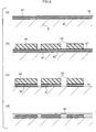
The capacitors 10A, 10B respectively have a laminate structure including electrode layers 11, 12 and a dielectric layer 13. The laminate structure of the capacitors 10A, 10B is shown in FIG. 5.
The electrode layer 11 is a lower electrode layer formed in a pattern on the substrate S, and has a laminate structure including an underlying adhesion layer 11 a, a main conductive layer 11 b and an adhesion metal layer 11 c in this embodiment, as shown in FIGS. 2 and 5. The underlying adhesion layer 11 a serves to secure sufficient adhesion between the substrate S and the electrode layer 11, and may preferably be constituted of Ti, Cr, or Ta. The underlying adhesion layer 11 a has a thickness of, for instance, 30 to 100 nm. The main conductive layer 11 b is the principal part of the electrode layer 11, engaged in electrical conduction which is the primary purpose thereof, and may be constituted of Cu, Au, Ag, or Al. The main conductive layer 11 b has a thickness of 0.5 to 2 μm, for instance. The adhesion metal layer 11 c, which serves to secure sufficient adhesion between the dielectric layer 13 and the electrode layer 11, includes an oxide coating 11 c′ formed on the surface of the adhesion metal layer 11 c confronting the dielectric layer 13 in this embodiment, as schematically shown in FIG. 5. In the present invention, the adhesion metal layer 11 c without the oxide coating 11 c′ provided on the surface thereof confronting the dielectric layer 13 may be employed, instead of the adhesion metal layer 11 c provided with such oxide coating 11 c′. Examples of the base metal material constituting the adhesion metal layer 11 c include Ti, Cr, and Ta. These are so-called easily oxidizable metals, which are oxidized under a relatively mild condition in a normal atmosphere. An overall thickness of the adhesion metal layer 11 c thus configured is, for instance, 30 to 100 nm.
The electrode layer 12 is an upper electrode layer formed so as to confront the electrode layer 11 via the dielectric layer 13, and has a laminate structure including an underlying adhesion layer 12 a and a main conductive layer 12 b in this embodiment, as shown in FIG. 5. The underlying adhesion layer 12 a serves to secure sufficient adhesion between the dielectric layer 13 and the electrode layer 12, and may be constituted of Ti, Cr, or Ta. The underlying adhesion layer 12 a has a thickness of, for instance, 30 to 100 nm. The main conductive layer 12 b is a principal part of the electrode layer 12, engaged in electrical conduction which is the primary purpose thereof, and may be constituted of Cu, Au, Ag, or Al. The main conductive layer 12 b may have a thickness of 1 to 15 μm. The electrode layer 12 may have a single layer structure instead of such laminate structure.
The dielectric layer 13 may preferably be constituted of an oxide dielectric or a nitride dielectric, such as silicon oxide, silicon nitride, aluminum oxide, tantalum oxide, or titanium oxide. The dielectric layer 13 may have a thickness of 0.1 to 1 μm.
The coil inductor 20 is a flat spiral coil patterned on the substrate S as shown in FIGS. 1 and 3, and has end portions 21, 22. Preferable materials of the coil inductor 20 include Cu, Au, Ag and Al.
The electrode pads 30A to 30D serve for external connection. The electrode pads 30A, 30B serve as terminals for ground connection, while the electrode pads 30C, 30D serve as input/output terminals of electrical signals. The electrode pads 30A to 30D may be constituted of a Ni body with the upper surface coated with a Au layer.
The interconnect 40 serves to electrically connect the components on the substrate S, and includes a first interconnect region 41 patterned on the substrate S, a second interconnect region 42 patterned mainly on the cover layer 50, and a third interconnect region 43 connecting the first interconnect region 41 and the second interconnect region 42, as shown in FIGS. 1 to 3. For the sake of explicitness of the drawings, only the first interconnect region 41 among the interconnects is indicated by hatching in FIG. 1. The first interconnect region 41 has a structure same as the multilayer structure of the electrode layer 11 of the capacitor units 10A, 10B, but without the adhesion metal layer 11 c. In other words, the first interconnect region 41 includes an underlying adhesion layer of the same composition and thickness as those of the underlying adhesion layer 11 a, and a main conductive layer of the same composition and thickness as those of the main conductive layer 11 b. A portion of the first interconnect region 41 constitutes the electrode layer 11. Preferable materials of the second interconnect region 42 and the third interconnect region 43 include Cu, Au, Ag, and Al. The second interconnect region 42 may have a thickness of 1 to 15 μm.
Referring to FIG. 4, the capacitor 10A is electrically connected to the electrode pads 30A, 30C and the coil inductor 20. More specifically, the electrode layer 11 of the capacitor 10A is electrically connected to the electrode pad 30A, and the electrode layer 12 of the capacitor 10A to the electrode pad 30C and the end portion 21 of the coil inductor 20. Likewise, the capacitor 10B is electrically connected to the electrode pads 30B, 30D and the coil inductor 20. More specifically, the electrode layer 11 of the capacitor 10B is electrically connected to the electrode pad 30B, and the electrode layer 12 of the capacitor 10B to the electrode pad 30D and the other end portion 22 of the coil inductor 20.
The cover layer 50 may be constituted of a polyimide or benzocyclobutene (BCB), and covers the capacitors 10A, 10B, the coil inductor 20, the first interconnect region 41, and the third interconnect region 43.
FIGS. 6( a) to 8(c) illustrate a manufacturing method of the integrated electronic component X. FIGS. 6( a) to 8(c) represent the progress of the formation process of a capacitor 10 (corresponding to the capacitor 10A, 10B), a part of the coil inductor 20, an electrode pad 30 (corresponding to the electrode pads 30A to 30D), and a part of an interconnect 40 shown in FIG. 8( c), in cross-sectional views of a region including these constituents. The cross-sectional views progressively depict a model of a plurality of predetermined regions included in a single section where the integrated electronic component is formed, on a material substrate to be processed.
To manufacture the integrated electronic component X, firstly an underlying layer 61, a main conductive layer 62, and a metal layer 63 with an oxide coating (not shown) provided on the surface thereof are consecutively formed on the substrate S as shown in FIG. 6( a), for example by a sputtering process. The underlying layer 61, the main conductive layer 62, and the metal layer 63 are respectively constituted of the materials cited regarding the underlying adhesion layer 11 a, the main conductive layer 11 b, and the adhesion metal layer 11 c of the electrode layer 11 of the capacitor 10. The metal layer 63 with the oxide coating may be formed by depositing an easily oxidizable metal such as Ti, Cr, or Ta on the main conductive layer 62, and exposing that metal to air. In the integrated electronic component X according to the present invention, when employing the adhesion metal layer 11 c without the oxide coating 11 c′ provided on the side of the dielectric layer 13, instead of the adhesion metal layer 11 c with the oxide coating 11 c′ on the side of the dielectric layer 13, the easily oxidizable metal is not exposed to air after being deposited on the main conductive layer 62, when forming the metal layer 63.
Then a resist pattern 64 is formed, as shown in FIG. 6( b). The resist pattern 64 has a pattern shape corresponding to the electrode layer 11 and the first interconnect region 41 of the capacitor 10. To form the resist pattern 64, a liquid photoresist is firstly deposited on the metal layer 63 by a spin coating process. The photoresist layer is then patterned through an exposure and a subsequent development process. The resist pattern and the cover layer to be described later may also be formed through a similar process.
Proceeding to FIG. 6( c), for example an ion milling process is performed utilizing the resist pattern 64 as the mask, so as to etch on the underlying layer 61, the main conductive layer 62, and the metal layer 63. A predetermined stripping solution is then applied to remove the resist pattern 64.
Then a dielectric layer 65 as shown in FIG. 6( d), by a sputtering process for instance. The dielectric layer 65 is constituted of one of the materials cited regarding the dielectric layer 13 of the capacitor 10.
Proceeding to FIG. 7( a), a resist pattern 66 is formed on the dielectric layer 65. The resist pattern 66 has a pattern shape corresponding to the dielectric layer 13 of the capacitor 10.
A wet etching process is then performed on the dielectric layer 65 utilizing the resist pattern 66 as the mask, as shown in FIG. 7( b). As a result, the dielectric layer 13 is shaped in a predetermined pattern. Suitable etching solutions for such wet etching process include buffered fluoric acid.
Then an exposed portion of the metal layer 63 is removed as shown in FIG. 7( c), by an etching process utilizing the resist pattern 66 and the dielectric layer 13 as the mask. At this stage, the electrode layer 11 and the first interconnect region 41 of the capacitor 10 are patterned. Suitable etching processes include an ion milling process and a wet etching process. Upon completing this process, the resist pattern 66 is removed.
Proceeding to FIG. 8( a), an electroplating process is performed with a predetermined resist pattern (not shown), so as to grow a conductive material at predetermined positions. At this stage, the electrode layer 12 of the capacitor 10, the coil inductor 20, and the main part of the electrode pad 30 are formed.
The cover layer 50 is then formed as shown in FIG. 8 b). The cover layer 50 is formed with openings 51, 52, 53, through which a portion of the electrode layer 12, a portion of the first interconnect region 41, and a portion of the main part of the electrode pad 30, respectively.
Finally as shown in FIG. 8( c), an electroplating process is performed with a predetermined resist pattern (not shown), so as to grow a conductive material at predetermined positions. As a result, the second interconnect region 42, the third interconnect region 43, and the surface layer of the electrode pad 30 are formed. Throughout the foregoing process, the integrated electronic component X shown in FIG. 1 can be manufactured.
Whereas the present invention is, as already stated, based on the finding that the lower electrode layer joined to the dielectric layer via a surface coating constituted of an easily oxidizable metal provided on the surface of the lower electrode layer can achieve superior adhesion to the dielectric layer, than the conventional lower electrode layer having the Ti/Au/Ni/Au multilayer structure, as well as on the finding that employing the lower electrode layer provided with such metal layer enables achieving a higher withstand voltage than employing the conventional lower electrode layer having the Ti/Au/Ni/Au multilayer structure, the electrode layer 11 (lower electrode layer) of the capacitor units 10A, 10B in the integrated electronic component X is joined to the dielectric layer 13 via the oxide coating 11 c′ (shown in FIG. 5) of the adhesion metal layer 11 c included in the electrode layer 11. The oxide coating 11 c′ has a metal oxide structure rooted in the metal foundation of the adhesion metal layer 11 c. The oxide coating 11 c′ having such metal oxide structure is readily combinable to the dielectric layer 13 (constituted of silicon oxide, silicon nitride, aluminum oxide, tantalum oxide, titanium oxide or the like). Accordingly, the electrode layer 11 can achieve excellent adhesion to the dielectric layer 13. Also, the oxide coating 11 c′ having the metal oxide structure blocks the flow of electrons from the metal foundation of the main conductive layer 11 b and the adhesion metal layer 11 c in the electrode layer 11 to the dielectric layer 13, thus granting a high withstand voltage to the capacitors 10A, 10B. Thus, the capacitors 10A, 10B of the integrated electronic component X can achieve excellent adhesion between the electrode layer 11 (lower electrode layer) and the dielectric layer 13, as well as a high withstand voltage.
WORKING EXAMPLE
A plurality of capacitor elements was fabricated according to the present invention. When forming the respective capacitors, capacitor units having a laminate structure configured as FIG. 5 under the following conditions, were made on a glass substrate. The underlying adhesion layer 11 a of the electrode layer 11 was a Ti layer of 50 nm in thickness. The main conductive layer 11 b was a Au layer of 1000 nm in thickness. The adhesion metal layer 11 c was a Ti layer of 50 nm in thickness, including an oxide coating on its surface. The electrode layer 12 was an electroplated Cu layer of 10 μm in thickness. The dielectric layer 13 was a SiO2 layer of 220 nm in thickness.
COMPARATIVE EXAMPLE
A plurality of capacitor elements was fabricated for comparison. To form the respective capacitor elements, similar capacitor units were fabricated on a glass substrate, except that the electrode layer 11 was substituted with the following lower electrode layer. The lower electrode layer according to the comparative example had a laminate structure including a Ti layer of 50 nm in thickness provided on the glass substrate, a first Au layer of 500 nm in thickness on the Ti layer, a Ni layer of 50 nm in thickness on the first Au layer, and a second Au layer of 500 nm in thickness on the Ni layer, and a minute amount of Ni originating from the Ni layer was brought to the surface of the second Au layer on the side of the dielectric layer, by thermal diffusion.
<Evaluation>
<High Temperature/High Humidity Test>
The plurality of capacitor elements according to the working example and those according to the comparative example were subjected to a high temperature/high humidity test. The capacitor elements were kept under a condition of 85 degree centigrade in environmental temperature and 95% in humidity, for 1000 hours. As a result, the plurality of capacitor elements according to the working example showed no variation in capacitance value before and after the test, and no delamination was observed between the electrode layer 11 (lower electrode layer) and the dielectric layer 13. In contrast, some of the capacitor elements according to the comparative example incurred a significant drop in capacitance after the test, and delamination was observed between the lower electrode layer and the dielectric layer, in those capacitor elements with the lowered capacitance. The delamination was confirmed by observation through a SEM with respect to predetermined cross-sections presented upon applying a focused ion beam (FIB) to the capacitor elements. Such result of the high temperature/high humidity test proves that the capacitor elements according to the working example are superior in adhesion between the lower electrode layer and the dielectric layer, to the capacitor elements according to the comparative example.
<Heat Resistance Test>
Another plurality of capacitor elements according to the working example and another plurality of capacitor elements according to the comparative example were subjected to a heat resistance test. The capacitor elements were subjected to four cycles of rise and fall of environmental temperature, in each of which the temperature was raised from 150 to 260 degree centigrade, and then lowered from 260 to 150 degree centigrade. As a result, no delamination was observed between the electrode layer 11 (lower electrode layer) and the dielectric layer 13 in the capacitor elements according to the working example. In contrast, delamination was observed between the lower electrode layer and the dielectric layer, in some of the capacitor elements according to the comparative example. The delamination was confirmed by observation through a SEM with respect to predetermined cross-sections presented upon applying a FIB to the capacitor elements. Such result of the heat resistance test also proves that the capacitor elements according to the working example are superior in adhesion between the lower electrode layer and the dielectric layer, to the capacitor elements according to the comparative example.
<Measurement of Withstand Voltage>
The withstand voltage was measured with respect to the capacitor elements according to the working example and the comparative example. The withstand voltages of the capacitor elements according to the working example and the comparative example were 230 V and 140 V respectively. Thus, the capacitor elements according to the working example proved to have a higher withstand voltage than the capacitor elements according to the comparative example.

Claims (14)

1. An electronic component comprising:
a substrate;
a capacitor unit having a laminate structure including a first electrode layer provided on the substrate, a second electrode layer opposed to the first electrode layer, and a dielectric layer disposed between the first and the second electrode layers; and
an interconnect layer provided on the substrate;
wherein the first electrode layer has a multilayer structure including an adhesion metal layer joined directly to the dielectric layer, the adhesion metal layer being provided with an oxide coating on a side of the dielectric layer;
wherein the interconnect layer has a multilayer structure same as the multilayer structure of the first electrode layer with the adhesion metal layer removed, and wherein the interconnect layer is continuous with a portion of the first electrode layer other than the adhesion metal layer.
2. The electronic component according to claim 1, wherein the adhesion metal layer contains a metal selected from a group consisting of Ti, Cr, and Ta.
3. An electronic component comprising:
a substrate;
a capacitor unit having a laminate structure including a first electrode layer provided on the substrate, a second electrode layer opposed to the first electrode layer, and a dielectric layer disposed between the first and the second electrode layers; and
an interconnect layer provided on the substrate;
wherein the first electrode layer has a multilayer structure including an adhesion metal layer that contains a metal selected from a group consisting of Ti, Cr, and Ta, and that is joined directly to the dielectric layer;
the interconnect layer has a multilayer structure same as the multilayer structure of the first electrode layer with the adhesion metal layer removed, and wherein the interconnect layer is continuous with a portion of the first electrode layer other than the adhesion metal layer.
4. The electronic component according to claim 2, wherein the first electrode layer includes an adhesion layer that contains the metal contained in the adhesion metal layer, and that is joined directly to the substrate.
5. The electronic component according to claim 1, wherein the first electrode layer includes a main conductive layer containing a metal selected from a group consisting of Cu, Au, Ag, and Al.
6. The electronic component according to claim 1, further comprising a passive component provided on the substrate, wherein the interconnect layer constitutes at least part of an electrical path between the passive component and the capacitor unit.
7. The electronic component according to claim 1, further comprising an electrode pad provided on the substrate, wherein the interconnect layer constitutes at least part of au electrical path between the electrode pad and the capacitor unit.
8. The electronic component according to claim 3, wherein the first electrode layer includes an adhesion layer that contains the metal contained in the adhesion metal layer, and that is joined directly to the substrate.
9. The electronic component according to claim 2, wherein the first electrode layer includes a main conductive layer containing a metal selected from a group consisting of Cu, Au, Ag, and Al.
10. The electronic component according to claim 3, wherein the first electrode layer includes a main conductive layer containing a metal selected from a group consisting of Cu, Au, Ag, and Al.
11. The electronic component according to claim 2, further comprising a passive component provided on the substrate, wherein the interconnect layer constitutes at least part of an electrical path between the passive component and the capacitor unit.
12. The electronic component according to claim 3, further comprising a passive component provided on the substrate, wherein the interconnect layer constitutes at least part of an electrical path between the passive component and the capacitor unit.
13. The electronic component according to claim 2, further comprising an electrode pad provided on the substrate, wherein the interconnect layer constitutes at least part of an electrical path between the electrode pad and the capacitor unit.
14. The electronic component according to claim 3, further comprising an electrode pad provided on the substrate, wherein the interconnect layer constitutes at least part of an electrical path between the electrode pad and the capacitor unit.
US11/585,877 2005-12-21 2006-10-25 Electronic component Expired - Fee Related US7855458B2 (en)

Applications Claiming Priority (2)

Application Number Priority Date Filing Date Title
JP2005367673A JP4916715B2 (en) 2005-12-21 2005-12-21 Electronic components
JP2005-367673 2005-12-21

Publications (2)

Publication Number Publication Date
US20070158848A1 US20070158848A1 (en) 2007-07-12
US7855458B2 true US7855458B2 (en) 2010-12-21

Family

ID=38184825

Family Applications (1)

Application Number Title Priority Date Filing Date
US11/585,877 Expired - Fee Related US7855458B2 (en) 2005-12-21 2006-10-25 Electronic component

Country Status (4)

Country Link
US (1) US7855458B2 (en)
JP (1) JP4916715B2 (en)
KR (1) KR100766213B1 (en)
CN (1) CN1988080B (en)

Cited By (1)

* Cited by examiner, † Cited by third party
Publication number Priority date Publication date Assignee Title
US20130221501A1 (en) * 2012-01-20 2013-08-29 Skyworks Solutions, Inc. Devices and methods related to interconnect conductors to reduce de-lamination

Families Citing this family (10)

* Cited by examiner, † Cited by third party
Publication number Priority date Publication date Assignee Title
US7544580B2 (en) * 2006-12-22 2009-06-09 United Microelectronics Corp. Method for manufacturing passive components
JP2009219268A (en) * 2008-03-11 2009-09-24 Daikin Ind Ltd Power conversion apparatus
JP5714361B2 (en) * 2011-03-01 2015-05-07 日本碍子株式会社 Terminal electrode forming method and method for manufacturing piezoelectric / electrostrictive element using the same
US9343403B2 (en) * 2014-04-04 2016-05-17 Qualcomm Incorporated Stress mitigation structure for wafer warpage reduction
US9893048B2 (en) 2015-09-14 2018-02-13 Qualcomm Incorporated Passive-on-glass (POG) device and method
US10476481B2 (en) * 2016-08-08 2019-11-12 Qorvo Us, Inc. Acoustic filtering circuitry including capacitor
JP6750462B2 (en) * 2016-11-04 2020-09-02 Tdk株式会社 Substrate with built-in thin film capacitors and electronic components
JP6725095B2 (en) 2018-06-21 2020-07-15 大日本印刷株式会社 Wiring board and semiconductor device
JP7266996B2 (en) 2018-11-20 2023-05-01 太陽誘電株式会社 Inductors, filters and multiplexers
WO2023106083A1 (en) * 2021-12-08 2023-06-15 株式会社村田製作所 Semiconductor device, matching circuit, and filter circuit

Citations (14)

* Cited by examiner, † Cited by third party
Publication number Priority date Publication date Assignee Title
JPH0461264A (en) 1990-06-29 1992-02-27 Nippon Telegr & Teleph Corp <Ntt> Ic composite device
JPH09102590A (en) 1995-10-05 1997-04-15 Ricoh Co Ltd Thin film capacitor
US6023407A (en) 1998-02-26 2000-02-08 International Business Machines Corporation Structure for a thin film multilayer capacitor
JP2000068645A (en) 1998-08-18 2000-03-03 Toshiba Chem Corp Manufacture of built-up multilayer printed wiring board
JP2002033239A (en) 2000-07-14 2002-01-31 Hitachi Ltd Lc filter
US20030211699A1 (en) * 2000-08-11 2003-11-13 Jun Lin Semiconductor device and its manufacture
US20030213615A1 (en) * 2002-05-16 2003-11-20 Mitsubishi Denki Kabushiki Kaisha Wiring board, fabrication method of wiring board, and semiconductor device
US20050037535A1 (en) * 2002-09-30 2005-02-17 Tsuyoshi Ogawa Method for fabricating high frequency module
US20050045891A1 (en) * 2003-08-29 2005-03-03 Semiconductor Energy Laboratory Co., Ltd. Electronics device, semiconductor deivce, and method for manufacturing the same
US20050104220A1 (en) * 2003-11-14 2005-05-19 Stanley Electric Co., Ltd. Semiconductor device and its manufacture method capable of preventing short circuit of electrodes when semiconductor device is mounted on sub-mount substrate
US20050175938A1 (en) * 2000-09-21 2005-08-11 Casper Michael D. Integrated thin film capacitor/inductor/interconnect system and method
US20060097344A1 (en) * 2001-09-21 2006-05-11 Casper Michael D Integrated thin film capacitor/inductor/interconnect system and method
US20060131069A1 (en) * 2004-12-20 2006-06-22 Noriyoshi Shimizu Method of manufacturing wiring substrate to which semiconductor chip is mounted
US20060157766A1 (en) * 2004-12-27 2006-07-20 Won Seok-Jun Metal-insulator-metal capacitor and method of fabricating the same

Family Cites Families (10)

* Cited by examiner, † Cited by third party
Publication number Priority date Publication date Assignee Title
JPH0354828A (en) * 1989-07-24 1991-03-08 Oki Electric Ind Co Ltd Compound conductor layer of semiconductor device, hole-making process of capacitor using compound conductor layer and compound conductor layer
JPH0745475A (en) * 1993-06-29 1995-02-14 Hitachi Ltd Thin film capacitor and fabrication thereof
JP3098923B2 (en) * 1994-12-28 2000-10-16 松下電子工業株式会社 Semiconductor device and manufacturing method thereof
US5807774A (en) * 1996-12-06 1998-09-15 Sharp Kabushiki Kaisha Simple method of fabricating ferroelectric capacitors
JP3623377B2 (en) * 1998-10-28 2005-02-23 シャープ株式会社 Manufacturing method of semiconductor device
JP2000349254A (en) * 1999-06-02 2000-12-15 Sony Corp Dielectric capacitor and memory, and their manufacture
JP2001094058A (en) * 1999-09-27 2001-04-06 Toshiba Corp Method for manufacturing semiconductor device
JP2002184946A (en) * 2000-12-11 2002-06-28 Murata Mfg Co Ltd Mim capacitor and its manufacturing method
JP2003045744A (en) 2001-07-26 2003-02-14 Kyocera Corp Thin film capacitor
JP2004221467A (en) * 2003-01-17 2004-08-05 Fujitsu Ltd Semiconductor device, and manufacturing method thereof

Patent Citations (14)

* Cited by examiner, † Cited by third party
Publication number Priority date Publication date Assignee Title
JPH0461264A (en) 1990-06-29 1992-02-27 Nippon Telegr & Teleph Corp <Ntt> Ic composite device
JPH09102590A (en) 1995-10-05 1997-04-15 Ricoh Co Ltd Thin film capacitor
US6023407A (en) 1998-02-26 2000-02-08 International Business Machines Corporation Structure for a thin film multilayer capacitor
JP2000068645A (en) 1998-08-18 2000-03-03 Toshiba Chem Corp Manufacture of built-up multilayer printed wiring board
JP2002033239A (en) 2000-07-14 2002-01-31 Hitachi Ltd Lc filter
US20030211699A1 (en) * 2000-08-11 2003-11-13 Jun Lin Semiconductor device and its manufacture
US20050175938A1 (en) * 2000-09-21 2005-08-11 Casper Michael D. Integrated thin film capacitor/inductor/interconnect system and method
US20060097344A1 (en) * 2001-09-21 2006-05-11 Casper Michael D Integrated thin film capacitor/inductor/interconnect system and method
US20030213615A1 (en) * 2002-05-16 2003-11-20 Mitsubishi Denki Kabushiki Kaisha Wiring board, fabrication method of wiring board, and semiconductor device
US20050037535A1 (en) * 2002-09-30 2005-02-17 Tsuyoshi Ogawa Method for fabricating high frequency module
US20050045891A1 (en) * 2003-08-29 2005-03-03 Semiconductor Energy Laboratory Co., Ltd. Electronics device, semiconductor deivce, and method for manufacturing the same
US20050104220A1 (en) * 2003-11-14 2005-05-19 Stanley Electric Co., Ltd. Semiconductor device and its manufacture method capable of preventing short circuit of electrodes when semiconductor device is mounted on sub-mount substrate
US20060131069A1 (en) * 2004-12-20 2006-06-22 Noriyoshi Shimizu Method of manufacturing wiring substrate to which semiconductor chip is mounted
US20060157766A1 (en) * 2004-12-27 2006-07-20 Won Seok-Jun Metal-insulator-metal capacitor and method of fabricating the same

Non-Patent Citations (1)

* Cited by examiner, † Cited by third party
Title
Search Report corresponding to Chinese application No. 200610144641X dated Mar. 20, 2009.

Cited By (3)

* Cited by examiner, † Cited by third party
Publication number Priority date Publication date Assignee Title
US20130221501A1 (en) * 2012-01-20 2013-08-29 Skyworks Solutions, Inc. Devices and methods related to interconnect conductors to reduce de-lamination
US9735117B2 (en) * 2012-01-20 2017-08-15 Skyworks Solutions, Inc. Devices and methods related to interconnect conductors to reduce de-lamination
US10020269B2 (en) 2012-01-20 2018-07-10 Skyworks Solutions. Inc. Devices and methods related to electrostatic discharge protection benign to radio-frequency operation

Also Published As

Publication number Publication date
JP2007173437A (en) 2007-07-05
KR20070067598A (en) 2007-06-28
CN1988080B (en) 2011-09-28
US20070158848A1 (en) 2007-07-12
CN1988080A (en) 2007-06-27
JP4916715B2 (en) 2012-04-18
KR100766213B1 (en) 2007-10-10

Similar Documents

Publication Publication Date Title
US7855458B2 (en) Electronic component
US7304339B2 (en) Passivation structure for ferroelectric thin-film devices
DE112004002038B4 (en) Acoustically coupled film transformer with increased common-mode rejection
US7808030B2 (en) Electronic component manufacturing method and electronic component
US20070045773A1 (en) Integrated electronic device and method of making the same
JP2009246401A (en) Method of forming highly reliable multi-layer circuit board
JP2005217419A (en) Integrated circuit inductor of high q factor (q value)
JP2000277693A (en) Integrated circuit with incorporated inductive element and manufacture of the same
KR100438160B1 (en) Device having inductor and capacitor and a fabrication method thereof
KR100881005B1 (en) Electronic component
US5915188A (en) Integrated inductor and capacitor on a substrate and method for fabricating same
EP1983532B1 (en) Capacitor and manufacturing method thereof
JP2009010114A (en) Dielectric thin-film capacitor
JP4447881B2 (en) Manufacturing method of interposer
KR20040004713A (en) Method for manufacturing surface acoustic wave device
EP2287892A2 (en) Passive device formed on glass substrate and fabrication method thereof
CN112530939B (en) Integrated capacitor and manufacturing method thereof, and radio frequency circuit
US20070293014A1 (en) Method for forming metal-insulator-metal capacitor of semiconductor device
CN112185887B (en) Manufacturing method of MIM capacitor
CN113257842A (en) Semiconductor device and method for integrating passive device
JP2003124591A (en) Electronic circuit board and its manufacturing method as well as copper-plating liquid for suppressing migration
JP3645808B2 (en) Thin-film electronic component, its manufacturing method and substrate
JP2009246181A (en) Electronic component
JP2001332441A (en) Single-plate capacitor
JPH09213568A (en) Capacitor and its manufacture

Legal Events

Date Code Title Description
AS Assignment

Owner name: FUJITSU LIMITED, JAPAN

Free format text: ASSIGNMENT OF ASSIGNORS INTEREST;ASSIGNORS:MATSUMOTO, TSUYOSHI;MIZUNO, YOSHIHIRO;MI, XIAOYU;AND OTHERS;REEL/FRAME:018467/0595

Effective date: 20060926

FEPP Fee payment procedure

Free format text: PAYOR NUMBER ASSIGNED (ORIGINAL EVENT CODE: ASPN); ENTITY STATUS OF PATENT OWNER: LARGE ENTITY

FPAY Fee payment

Year of fee payment: 4

FEPP Fee payment procedure

Free format text: MAINTENANCE FEE REMINDER MAILED (ORIGINAL EVENT CODE: REM.)

LAPS Lapse for failure to pay maintenance fees

Free format text: PATENT EXPIRED FOR FAILURE TO PAY MAINTENANCE FEES (ORIGINAL EVENT CODE: EXP.); ENTITY STATUS OF PATENT OWNER: LARGE ENTITY

STCH Information on status: patent discontinuation

Free format text: PATENT EXPIRED DUE TO NONPAYMENT OF MAINTENANCE FEES UNDER 37 CFR 1.362

FP Lapsed due to failure to pay maintenance fee

Effective date: 20181221