US8022406B2 - Light emitting device - Google Patents
Light emitting device Download PDFInfo
- Publication number
- US8022406B2 US8022406B2 US12/358,843 US35884309A US8022406B2 US 8022406 B2 US8022406 B2 US 8022406B2 US 35884309 A US35884309 A US 35884309A US 8022406 B2 US8022406 B2 US 8022406B2
- Authority
- US
- United States
- Prior art keywords
- light
- emitting
- transistor
- emitting transistor
- switching element
- Prior art date
- Legal status (The legal status is an assumption and is not a legal conclusion. Google has not performed a legal analysis and makes no representation as to the accuracy of the status listed.)
- Expired - Fee Related
Links
- 239000010408 film Substances 0.000 description 128
- 239000004065 semiconductor Substances 0.000 description 77
- 239000010410 layer Substances 0.000 description 66
- 238000000034 method Methods 0.000 description 59
- 239000000463 material Substances 0.000 description 54
- 239000003990 capacitor Substances 0.000 description 40
- 238000003860 storage Methods 0.000 description 40
- 239000000758 substrate Substances 0.000 description 40
- 239000012535 impurity Substances 0.000 description 27
- 150000001875 compounds Chemical class 0.000 description 22
- CNQCVBJFEGMYDW-UHFFFAOYSA-N lawrencium atom Chemical compound [Lr] CNQCVBJFEGMYDW-UHFFFAOYSA-N 0.000 description 19
- 239000002585 base Substances 0.000 description 16
- 238000010586 diagram Methods 0.000 description 15
- 239000004973 liquid crystal related substance Substances 0.000 description 14
- 229910052581 Si3N4 Inorganic materials 0.000 description 11
- XUIMIQQOPSSXEZ-UHFFFAOYSA-N Silicon Chemical compound [Si] XUIMIQQOPSSXEZ-UHFFFAOYSA-N 0.000 description 11
- 239000010703 silicon Substances 0.000 description 11
- HQVNEWCFYHHQES-UHFFFAOYSA-N silicon nitride Chemical compound N12[Si]34N5[Si]62N3[Si]51N64 HQVNEWCFYHHQES-UHFFFAOYSA-N 0.000 description 11
- IJGRMHOSHXDMSA-UHFFFAOYSA-N Atomic nitrogen Chemical compound N#N IJGRMHOSHXDMSA-UHFFFAOYSA-N 0.000 description 10
- 239000010949 copper Substances 0.000 description 10
- 229910052751 metal Inorganic materials 0.000 description 10
- 239000002184 metal Substances 0.000 description 10
- ORQBXQOJMQIAOY-UHFFFAOYSA-N nobelium Chemical compound [No] ORQBXQOJMQIAOY-UHFFFAOYSA-N 0.000 description 10
- 229910052710 silicon Inorganic materials 0.000 description 10
- 239000011229 interlayer Substances 0.000 description 9
- -1 polyethylene terephthalate Polymers 0.000 description 9
- 239000010936 titanium Substances 0.000 description 8
- VYPSYNLAJGMNEJ-UHFFFAOYSA-N silicon dioxide Inorganic materials O=[Si]=O VYPSYNLAJGMNEJ-UHFFFAOYSA-N 0.000 description 7
- 229910052814 silicon oxide Inorganic materials 0.000 description 7
- 238000004544 sputter deposition Methods 0.000 description 7
- PXHVJJICTQNCMI-UHFFFAOYSA-N Nickel Chemical compound [Ni] PXHVJJICTQNCMI-UHFFFAOYSA-N 0.000 description 6
- UCKMPCXJQFINFW-UHFFFAOYSA-N Sulphide Chemical compound [S-2] UCKMPCXJQFINFW-UHFFFAOYSA-N 0.000 description 6
- 229910052782 aluminium Inorganic materials 0.000 description 6
- XAGFODPZIPBFFR-UHFFFAOYSA-N aluminium Chemical compound [Al] XAGFODPZIPBFFR-UHFFFAOYSA-N 0.000 description 6
- QVGXLLKOCUKJST-UHFFFAOYSA-N atomic oxygen Chemical compound [O] QVGXLLKOCUKJST-UHFFFAOYSA-N 0.000 description 6
- 230000008859 change Effects 0.000 description 6
- 238000005229 chemical vapour deposition Methods 0.000 description 6
- 239000000460 chlorine Substances 0.000 description 6
- 238000001704 evaporation Methods 0.000 description 6
- 239000010931 gold Substances 0.000 description 6
- 239000011777 magnesium Substances 0.000 description 6
- 239000001301 oxygen Substances 0.000 description 6
- 229910052760 oxygen Inorganic materials 0.000 description 6
- BASFCYQUMIYNBI-UHFFFAOYSA-N platinum Chemical compound [Pt] BASFCYQUMIYNBI-UHFFFAOYSA-N 0.000 description 6
- 238000005070 sampling Methods 0.000 description 6
- 239000010409 thin film Substances 0.000 description 6
- RYGMFSIKBFXOCR-UHFFFAOYSA-N Copper Chemical compound [Cu] RYGMFSIKBFXOCR-UHFFFAOYSA-N 0.000 description 5
- PXGOKWXKJXAPGV-UHFFFAOYSA-N Fluorine Chemical compound FF PXGOKWXKJXAPGV-UHFFFAOYSA-N 0.000 description 5
- UFHFLCQGNIYNRP-UHFFFAOYSA-N Hydrogen Chemical compound [H][H] UFHFLCQGNIYNRP-UHFFFAOYSA-N 0.000 description 5
- 239000005083 Zinc sulfide Substances 0.000 description 5
- 229910045601 alloy Inorganic materials 0.000 description 5
- 239000000956 alloy Substances 0.000 description 5
- 239000011575 calcium Substances 0.000 description 5
- 229910052802 copper Inorganic materials 0.000 description 5
- 229910052731 fluorine Inorganic materials 0.000 description 5
- 239000011737 fluorine Substances 0.000 description 5
- 239000001257 hydrogen Substances 0.000 description 5
- 229910052739 hydrogen Inorganic materials 0.000 description 5
- 238000004519 manufacturing process Methods 0.000 description 5
- 229910052757 nitrogen Inorganic materials 0.000 description 5
- 230000004044 response Effects 0.000 description 5
- 229910052984 zinc sulfide Inorganic materials 0.000 description 5
- SKJCKYVIQGBWTN-UHFFFAOYSA-N (4-hydroxyphenyl) methanesulfonate Chemical compound CS(=O)(=O)OC1=CC=C(O)C=C1 SKJCKYVIQGBWTN-UHFFFAOYSA-N 0.000 description 4
- WUPHOULIZUERAE-UHFFFAOYSA-N 3-(oxolan-2-yl)propanoic acid Chemical compound OC(=O)CCC1CCCO1 WUPHOULIZUERAE-UHFFFAOYSA-N 0.000 description 4
- RTAQQCXQSZGOHL-UHFFFAOYSA-N Titanium Chemical compound [Ti] RTAQQCXQSZGOHL-UHFFFAOYSA-N 0.000 description 4
- 125000004429 atom Chemical group 0.000 description 4
- 229910002113 barium titanate Inorganic materials 0.000 description 4
- 229910052980 cadmium sulfide Inorganic materials 0.000 description 4
- 239000011651 chromium Substances 0.000 description 4
- 238000000576 coating method Methods 0.000 description 4
- KPUWHANPEXNPJT-UHFFFAOYSA-N disiloxane Chemical class [SiH3]O[SiH3] KPUWHANPEXNPJT-UHFFFAOYSA-N 0.000 description 4
- 230000006870 function Effects 0.000 description 4
- 150000002484 inorganic compounds Chemical class 0.000 description 4
- 229910010272 inorganic material Inorganic materials 0.000 description 4
- 239000011810 insulating material Substances 0.000 description 4
- TWNQGVIAIRXVLR-UHFFFAOYSA-N oxo(oxoalumanyloxy)alumane Chemical compound O=[Al]O[Al]=O TWNQGVIAIRXVLR-UHFFFAOYSA-N 0.000 description 4
- SIWVEOZUMHYXCS-UHFFFAOYSA-N oxo(oxoyttriooxy)yttrium Chemical compound O=[Y]O[Y]=O SIWVEOZUMHYXCS-UHFFFAOYSA-N 0.000 description 4
- RVTZCBVAJQQJTK-UHFFFAOYSA-N oxygen(2-);zirconium(4+) Chemical compound [O-2].[O-2].[Zr+4] RVTZCBVAJQQJTK-UHFFFAOYSA-N 0.000 description 4
- 230000008569 process Effects 0.000 description 4
- 239000002356 single layer Substances 0.000 description 4
- 238000003746 solid phase reaction Methods 0.000 description 4
- 239000000126 substance Substances 0.000 description 4
- 229910052719 titanium Inorganic materials 0.000 description 4
- 229910001928 zirconium oxide Inorganic materials 0.000 description 4
- OYPRJOBELJOOCE-UHFFFAOYSA-N Calcium Chemical compound [Ca] OYPRJOBELJOOCE-UHFFFAOYSA-N 0.000 description 3
- ZAMOUSCENKQFHK-UHFFFAOYSA-N Chlorine atom Chemical compound [Cl] ZAMOUSCENKQFHK-UHFFFAOYSA-N 0.000 description 3
- ZOKXTWBITQBERF-UHFFFAOYSA-N Molybdenum Chemical compound [Mo] ZOKXTWBITQBERF-UHFFFAOYSA-N 0.000 description 3
- KDLHZDBZIXYQEI-UHFFFAOYSA-N Palladium Chemical compound [Pd] KDLHZDBZIXYQEI-UHFFFAOYSA-N 0.000 description 3
- BQCADISMDOOEFD-UHFFFAOYSA-N Silver Chemical compound [Ag] BQCADISMDOOEFD-UHFFFAOYSA-N 0.000 description 3
- XLOMVQKBTHCTTD-UHFFFAOYSA-N Zinc monoxide Chemical compound [Zn]=O XLOMVQKBTHCTTD-UHFFFAOYSA-N 0.000 description 3
- 229910052791 calcium Inorganic materials 0.000 description 3
- 229910052801 chlorine Inorganic materials 0.000 description 3
- 238000001678 elastic recoil detection analysis Methods 0.000 description 3
- 229910052733 gallium Inorganic materials 0.000 description 3
- 239000007789 gas Substances 0.000 description 3
- PCHJSUWPFVWCPO-UHFFFAOYSA-N gold Chemical compound [Au] PCHJSUWPFVWCPO-UHFFFAOYSA-N 0.000 description 3
- 229910052737 gold Inorganic materials 0.000 description 3
- 239000007791 liquid phase Substances 0.000 description 3
- 229910052750 molybdenum Inorganic materials 0.000 description 3
- 239000011733 molybdenum Substances 0.000 description 3
- 150000004767 nitrides Chemical class 0.000 description 3
- 239000002245 particle Substances 0.000 description 3
- 238000005268 plasma chemical vapour deposition Methods 0.000 description 3
- 239000004033 plastic Substances 0.000 description 3
- 229920003023 plastic Polymers 0.000 description 3
- 238000005001 rutherford backscattering spectroscopy Methods 0.000 description 3
- 229910052709 silver Inorganic materials 0.000 description 3
- 239000004332 silver Substances 0.000 description 3
- 238000010532 solid phase synthesis reaction Methods 0.000 description 3
- 125000001424 substituent group Chemical group 0.000 description 3
- 238000005303 weighing Methods 0.000 description 3
- PFNQVRZLDWYSCW-UHFFFAOYSA-N (fluoren-9-ylideneamino) n-naphthalen-1-ylcarbamate Chemical compound C12=CC=CC=C2C2=CC=CC=C2C1=NOC(=O)NC1=CC=CC2=CC=CC=C12 PFNQVRZLDWYSCW-UHFFFAOYSA-N 0.000 description 2
- MBXOOYPCIDHXGH-UHFFFAOYSA-N 3-butylpentane-2,4-dione Chemical compound CCCCC(C(C)=O)C(C)=O MBXOOYPCIDHXGH-UHFFFAOYSA-N 0.000 description 2
- XMWRBQBLMFGWIX-UHFFFAOYSA-N C60 fullerene Chemical compound C12=C3C(C4=C56)=C7C8=C5C5=C9C%10=C6C6=C4C1=C1C4=C6C6=C%10C%10=C9C9=C%11C5=C8C5=C8C7=C3C3=C7C2=C1C1=C2C4=C6C4=C%10C6=C9C9=C%11C5=C5C8=C3C3=C7C1=C1C2=C4C6=C2C9=C5C3=C12 XMWRBQBLMFGWIX-UHFFFAOYSA-N 0.000 description 2
- OKTJSMMVPCPJKN-UHFFFAOYSA-N Carbon Chemical compound [C] OKTJSMMVPCPJKN-UHFFFAOYSA-N 0.000 description 2
- KZBUYRJDOAKODT-UHFFFAOYSA-N Chlorine Chemical compound ClCl KZBUYRJDOAKODT-UHFFFAOYSA-N 0.000 description 2
- VYZAMTAEIAYCRO-UHFFFAOYSA-N Chromium Chemical compound [Cr] VYZAMTAEIAYCRO-UHFFFAOYSA-N 0.000 description 2
- 229910052693 Europium Inorganic materials 0.000 description 2
- FYYHWMGAXLPEAU-UHFFFAOYSA-N Magnesium Chemical compound [Mg] FYYHWMGAXLPEAU-UHFFFAOYSA-N 0.000 description 2
- 239000004695 Polyether sulfone Substances 0.000 description 2
- 239000004642 Polyimide Substances 0.000 description 2
- 239000004743 Polypropylene Substances 0.000 description 2
- GWEVSGVZZGPLCZ-UHFFFAOYSA-N Titan oxide Chemical compound O=[Ti]=O GWEVSGVZZGPLCZ-UHFFFAOYSA-N 0.000 description 2
- 206010047571 Visual impairment Diseases 0.000 description 2
- NIXOWILDQLNWCW-UHFFFAOYSA-N acrylic acid group Chemical group C(C=C)(=O)O NIXOWILDQLNWCW-UHFFFAOYSA-N 0.000 description 2
- 229910052783 alkali metal Inorganic materials 0.000 description 2
- 150000001340 alkali metals Chemical class 0.000 description 2
- 229910052784 alkaline earth metal Inorganic materials 0.000 description 2
- 150000001342 alkaline earth metals Chemical class 0.000 description 2
- HSFWRNGVRCDJHI-UHFFFAOYSA-N alpha-acetylene Natural products C#C HSFWRNGVRCDJHI-UHFFFAOYSA-N 0.000 description 2
- COOGPNLGKIHLSK-UHFFFAOYSA-N aluminium sulfide Chemical compound [Al+3].[Al+3].[S-2].[S-2].[S-2] COOGPNLGKIHLSK-UHFFFAOYSA-N 0.000 description 2
- 238000003877 atomic layer epitaxy Methods 0.000 description 2
- CJDPJFRMHVXWPT-UHFFFAOYSA-N barium sulfide Chemical compound [S-2].[Ba+2] CJDPJFRMHVXWPT-UHFFFAOYSA-N 0.000 description 2
- JRPBQTZRNDNNOP-UHFFFAOYSA-N barium titanate Chemical compound [Ba+2].[Ba+2].[O-][Ti]([O-])([O-])[O-] JRPBQTZRNDNNOP-UHFFFAOYSA-N 0.000 description 2
- 230000005540 biological transmission Effects 0.000 description 2
- JGIATAMCQXIDNZ-UHFFFAOYSA-N calcium sulfide Chemical compound [Ca]=S JGIATAMCQXIDNZ-UHFFFAOYSA-N 0.000 description 2
- 239000003575 carbonaceous material Substances 0.000 description 2
- 239000000969 carrier Substances 0.000 description 2
- 229910052804 chromium Inorganic materials 0.000 description 2
- 238000000975 co-precipitation Methods 0.000 description 2
- 229910017052 cobalt Inorganic materials 0.000 description 2
- 239000010941 cobalt Substances 0.000 description 2
- GUTLYIVDDKVIGB-UHFFFAOYSA-N cobalt atom Chemical compound [Co] GUTLYIVDDKVIGB-UHFFFAOYSA-N 0.000 description 2
- 229920000547 conjugated polymer Polymers 0.000 description 2
- 238000005401 electroluminescence Methods 0.000 description 2
- 238000005530 etching Methods 0.000 description 2
- OGPBJKLSAFTDLK-UHFFFAOYSA-N europium atom Chemical compound [Eu] OGPBJKLSAFTDLK-UHFFFAOYSA-N 0.000 description 2
- 230000005669 field effect Effects 0.000 description 2
- 229910003472 fullerene Inorganic materials 0.000 description 2
- CJNBYAVZURUTKZ-UHFFFAOYSA-N hafnium(iv) oxide Chemical compound O=[Hf]=O CJNBYAVZURUTKZ-UHFFFAOYSA-N 0.000 description 2
- 238000010438 heat treatment Methods 0.000 description 2
- AMGQUBHHOARCQH-UHFFFAOYSA-N indium;oxotin Chemical compound [In].[Sn]=O AMGQUBHHOARCQH-UHFFFAOYSA-N 0.000 description 2
- 229910052749 magnesium Inorganic materials 0.000 description 2
- 239000011572 manganese Substances 0.000 description 2
- 238000005259 measurement Methods 0.000 description 2
- 230000007246 mechanism Effects 0.000 description 2
- 239000007769 metal material Substances 0.000 description 2
- 239000004570 mortar (masonry) Substances 0.000 description 2
- 229910052759 nickel Inorganic materials 0.000 description 2
- 150000002894 organic compounds Chemical class 0.000 description 2
- 239000011368 organic material Substances 0.000 description 2
- BPUBBGLMJRNUCC-UHFFFAOYSA-N oxygen(2-);tantalum(5+) Chemical compound [O-2].[O-2].[O-2].[O-2].[O-2].[Ta+5].[Ta+5] BPUBBGLMJRNUCC-UHFFFAOYSA-N 0.000 description 2
- 238000000059 patterning Methods 0.000 description 2
- 239000008188 pellet Substances 0.000 description 2
- 238000005240 physical vapour deposition Methods 0.000 description 2
- 229910052697 platinum Inorganic materials 0.000 description 2
- 229920003207 poly(ethylene-2,6-naphthalate) Polymers 0.000 description 2
- 229920001197 polyacetylene Polymers 0.000 description 2
- 229920000767 polyaniline Polymers 0.000 description 2
- 229920006393 polyether sulfone Polymers 0.000 description 2
- 239000011112 polyethylene naphthalate Substances 0.000 description 2
- 229920000139 polyethylene terephthalate Polymers 0.000 description 2
- 239000005020 polyethylene terephthalate Substances 0.000 description 2
- 229920001721 polyimide Polymers 0.000 description 2
- 229920001155 polypropylene Polymers 0.000 description 2
- 229920000128 polypyrrole Polymers 0.000 description 2
- 229920000123 polythiophene Polymers 0.000 description 2
- 239000000843 powder Substances 0.000 description 2
- 229910052761 rare earth metal Inorganic materials 0.000 description 2
- 150000002910 rare earth metals Chemical class 0.000 description 2
- 239000011734 sodium Substances 0.000 description 2
- 229910052721 tungsten Inorganic materials 0.000 description 2
- 239000010937 tungsten Substances 0.000 description 2
- 239000011701 zinc Substances 0.000 description 2
- DRDVZXDWVBGGMH-UHFFFAOYSA-N zinc;sulfide Chemical compound [S-2].[Zn+2] DRDVZXDWVBGGMH-UHFFFAOYSA-N 0.000 description 2
- 229910017073 AlLi Inorganic materials 0.000 description 1
- PIGFYZPCRLYGLF-UHFFFAOYSA-N Aluminum nitride Chemical compound [Al]#N PIGFYZPCRLYGLF-UHFFFAOYSA-N 0.000 description 1
- JBRZTFJDHDCESZ-UHFFFAOYSA-N AsGa Chemical compound [As]#[Ga] JBRZTFJDHDCESZ-UHFFFAOYSA-N 0.000 description 1
- 229910015844 BCl3 Inorganic materials 0.000 description 1
- 229910052684 Cerium Inorganic materials 0.000 description 1
- 229910052691 Erbium Inorganic materials 0.000 description 1
- GYHNNYVSQQEPJS-UHFFFAOYSA-N Gallium Chemical compound [Ga] GYHNNYVSQQEPJS-UHFFFAOYSA-N 0.000 description 1
- 229910001218 Gallium arsenide Inorganic materials 0.000 description 1
- JMASRVWKEDWRBT-UHFFFAOYSA-N Gallium nitride Chemical compound [Ga]#N JMASRVWKEDWRBT-UHFFFAOYSA-N 0.000 description 1
- DGAQECJNVWCQMB-PUAWFVPOSA-M Ilexoside XXIX Chemical compound C[C@@H]1CC[C@@]2(CC[C@@]3(C(=CC[C@H]4[C@]3(CC[C@@H]5[C@@]4(CC[C@@H](C5(C)C)OS(=O)(=O)[O-])C)C)[C@@H]2[C@]1(C)O)C)C(=O)O[C@H]6[C@@H]([C@H]([C@@H]([C@H](O6)CO)O)O)O.[Na+] DGAQECJNVWCQMB-PUAWFVPOSA-M 0.000 description 1
- XEEYBQQBJWHFJM-UHFFFAOYSA-N Iron Chemical compound [Fe] XEEYBQQBJWHFJM-UHFFFAOYSA-N 0.000 description 1
- 239000002841 Lewis acid Substances 0.000 description 1
- WHXSMMKQMYFTQS-UHFFFAOYSA-N Lithium Chemical compound [Li] WHXSMMKQMYFTQS-UHFFFAOYSA-N 0.000 description 1
- PWHULOQIROXLJO-UHFFFAOYSA-N Manganese Chemical compound [Mn] PWHULOQIROXLJO-UHFFFAOYSA-N 0.000 description 1
- 229910003781 PbTiO3 Inorganic materials 0.000 description 1
- 239000004697 Polyetherimide Substances 0.000 description 1
- 239000004721 Polyphenylene oxide Substances 0.000 description 1
- 239000004734 Polyphenylene sulfide Substances 0.000 description 1
- 239000004954 Polyphthalamide Substances 0.000 description 1
- 229910052777 Praseodymium Inorganic materials 0.000 description 1
- 229910052772 Samarium Inorganic materials 0.000 description 1
- 229910052771 Terbium Inorganic materials 0.000 description 1
- 229910052775 Thulium Inorganic materials 0.000 description 1
- NRTOMJZYCJJWKI-UHFFFAOYSA-N Titanium nitride Chemical compound [Ti]#N NRTOMJZYCJJWKI-UHFFFAOYSA-N 0.000 description 1
- 229910052769 Ytterbium Inorganic materials 0.000 description 1
- 239000002253 acid Substances 0.000 description 1
- 125000000217 alkyl group Chemical group 0.000 description 1
- 150000004945 aromatic hydrocarbons Chemical class 0.000 description 1
- NWAIGJYBQQYSPW-UHFFFAOYSA-N azanylidyneindigane Chemical compound [In]#N NWAIGJYBQQYSPW-UHFFFAOYSA-N 0.000 description 1
- GPBUGPUPKAGMDK-UHFFFAOYSA-N azanylidynemolybdenum Chemical compound [Mo]#N GPBUGPUPKAGMDK-UHFFFAOYSA-N 0.000 description 1
- 229910052788 barium Inorganic materials 0.000 description 1
- DSAJWYNOEDNPEQ-UHFFFAOYSA-N barium atom Chemical compound [Ba] DSAJWYNOEDNPEQ-UHFFFAOYSA-N 0.000 description 1
- 230000004888 barrier function Effects 0.000 description 1
- 239000011230 binding agent Substances 0.000 description 1
- 229910052792 caesium Inorganic materials 0.000 description 1
- TVFDJXOCXUVLDH-UHFFFAOYSA-N caesium atom Chemical compound [Cs] TVFDJXOCXUVLDH-UHFFFAOYSA-N 0.000 description 1
- 239000006229 carbon black Substances 0.000 description 1
- 239000002041 carbon nanotube Substances 0.000 description 1
- 229910021393 carbon nanotube Inorganic materials 0.000 description 1
- 230000001413 cellular effect Effects 0.000 description 1
- GWXLDORMOJMVQZ-UHFFFAOYSA-N cerium Chemical compound [Ce] GWXLDORMOJMVQZ-UHFFFAOYSA-N 0.000 description 1
- 238000006243 chemical reaction Methods 0.000 description 1
- 239000003086 colorant Substances 0.000 description 1
- PMHQVHHXPFUNSP-UHFFFAOYSA-M copper(1+);methylsulfanylmethane;bromide Chemical compound Br[Cu].CSC PMHQVHHXPFUNSP-UHFFFAOYSA-M 0.000 description 1
- OXBLHERUFWYNTN-UHFFFAOYSA-M copper(I) chloride Chemical compound [Cu]Cl OXBLHERUFWYNTN-UHFFFAOYSA-M 0.000 description 1
- AQKDYYAZGHBAPR-UHFFFAOYSA-M copper;copper(1+);sulfanide Chemical compound [SH-].[Cu].[Cu+] AQKDYYAZGHBAPR-UHFFFAOYSA-M 0.000 description 1
- 239000013078 crystal Substances 0.000 description 1
- 238000000354 decomposition reaction Methods 0.000 description 1
- 229910003460 diamond Inorganic materials 0.000 description 1
- 239000010432 diamond Substances 0.000 description 1
- NKZSPGSOXYXWQA-UHFFFAOYSA-N dioxido(oxo)titanium;lead(2+) Chemical compound [Pb+2].[O-][Ti]([O-])=O NKZSPGSOXYXWQA-UHFFFAOYSA-N 0.000 description 1
- 238000007598 dipping method Methods 0.000 description 1
- 239000006185 dispersion Substances 0.000 description 1
- 238000001312 dry etching Methods 0.000 description 1
- 230000000694 effects Effects 0.000 description 1
- 230000005684 electric field Effects 0.000 description 1
- 230000005685 electric field effect Effects 0.000 description 1
- 238000007772 electroless plating Methods 0.000 description 1
- 238000005566 electron beam evaporation Methods 0.000 description 1
- 238000009713 electroplating Methods 0.000 description 1
- UYAHIZSMUZPPFV-UHFFFAOYSA-N erbium Chemical compound [Er] UYAHIZSMUZPPFV-UHFFFAOYSA-N 0.000 description 1
- 230000008020 evaporation Effects 0.000 description 1
- 238000004108 freeze drying Methods 0.000 description 1
- BVSHTEBQPBBCFT-UHFFFAOYSA-N gallium(iii) sulfide Chemical compound [S-2].[S-2].[S-2].[Ga+3].[Ga+3] BVSHTEBQPBBCFT-UHFFFAOYSA-N 0.000 description 1
- 229910052732 germanium Inorganic materials 0.000 description 1
- GNPVGFCGXDBREM-UHFFFAOYSA-N germanium atom Chemical compound [Ge] GNPVGFCGXDBREM-UHFFFAOYSA-N 0.000 description 1
- 239000011521 glass Substances 0.000 description 1
- 229910002804 graphite Inorganic materials 0.000 description 1
- 239000010439 graphite Substances 0.000 description 1
- 229910052736 halogen Inorganic materials 0.000 description 1
- 125000005843 halogen group Chemical group 0.000 description 1
- 150000002367 halogens Chemical class 0.000 description 1
- 150000004678 hydrides Chemical class 0.000 description 1
- 229910003437 indium oxide Inorganic materials 0.000 description 1
- PJXISJQVUVHSOJ-UHFFFAOYSA-N indium(iii) oxide Chemical compound [O-2].[O-2].[O-2].[In+3].[In+3] PJXISJQVUVHSOJ-UHFFFAOYSA-N 0.000 description 1
- 238000002347 injection Methods 0.000 description 1
- 239000007924 injection Substances 0.000 description 1
- 150000007517 lewis acids Chemical class 0.000 description 1
- 229910052744 lithium Inorganic materials 0.000 description 1
- 229910052748 manganese Inorganic materials 0.000 description 1
- 239000011159 matrix material Substances 0.000 description 1
- 150000002736 metal compounds Chemical class 0.000 description 1
- 229910021645 metal ion Inorganic materials 0.000 description 1
- 229910044991 metal oxide Inorganic materials 0.000 description 1
- 150000004706 metal oxides Chemical class 0.000 description 1
- 229920003240 metallophthalocyanine polymer Polymers 0.000 description 1
- 150000002739 metals Chemical class 0.000 description 1
- 238000002156 mixing Methods 0.000 description 1
- MZYHMUONCNKCHE-UHFFFAOYSA-N naphthalene-1,2,3,4-tetracarboxylic acid Chemical compound C1=CC=CC2=C(C(O)=O)C(C(=O)O)=C(C(O)=O)C(C(O)=O)=C21 MZYHMUONCNKCHE-UHFFFAOYSA-N 0.000 description 1
- URLJKFSTXLNXLG-UHFFFAOYSA-N niobium(5+);oxygen(2-) Chemical compound [O-2].[O-2].[O-2].[O-2].[O-2].[Nb+5].[Nb+5] URLJKFSTXLNXLG-UHFFFAOYSA-N 0.000 description 1
- 238000005457 optimization Methods 0.000 description 1
- AHLBNYSZXLDEJQ-FWEHEUNISA-N orlistat Chemical compound CCCCCCCCCCC[C@H](OC(=O)[C@H](CC(C)C)NC=O)C[C@@H]1OC(=O)[C@H]1CCCCCC AHLBNYSZXLDEJQ-FWEHEUNISA-N 0.000 description 1
- 229910052763 palladium Inorganic materials 0.000 description 1
- SLIUAWYAILUBJU-UHFFFAOYSA-N pentacene Chemical compound C1=CC=CC2=CC3=CC4=CC5=CC=CC=C5C=C4C=C3C=C21 SLIUAWYAILUBJU-UHFFFAOYSA-N 0.000 description 1
- 230000000737 periodic effect Effects 0.000 description 1
- FVDOBFPYBSDRKH-UHFFFAOYSA-N perylene-3,4,9,10-tetracarboxylic acid Chemical compound C=12C3=CC=C(C(O)=O)C2=C(C(O)=O)C=CC=1C1=CC=C(C(O)=O)C2=C1C3=CC=C2C(=O)O FVDOBFPYBSDRKH-UHFFFAOYSA-N 0.000 description 1
- 238000000206 photolithography Methods 0.000 description 1
- IEQIEDJGQAUEQZ-UHFFFAOYSA-N phthalocyanine Chemical compound N1C(N=C2C3=CC=CC=C3C(N=C3C4=CC=CC=C4C(=N4)N3)=N2)=C(C=CC=C2)C2=C1N=C1C2=CC=CC=C2C4=N1 IEQIEDJGQAUEQZ-UHFFFAOYSA-N 0.000 description 1
- 229920002492 poly(sulfone) Polymers 0.000 description 1
- 239000004417 polycarbonate Substances 0.000 description 1
- 229920000515 polycarbonate Polymers 0.000 description 1
- 229920000015 polydiacetylene Polymers 0.000 description 1
- 229920001601 polyetherimide Polymers 0.000 description 1
- 229920000642 polymer Polymers 0.000 description 1
- 229920006380 polyphenylene oxide Polymers 0.000 description 1
- 229920000069 polyphenylene sulfide Polymers 0.000 description 1
- 229920006375 polyphtalamide Polymers 0.000 description 1
- 229920002717 polyvinylpyridine Polymers 0.000 description 1
- PUDIUYLPXJFUGB-UHFFFAOYSA-N praseodymium atom Chemical compound [Pr] PUDIUYLPXJFUGB-UHFFFAOYSA-N 0.000 description 1
- 239000002243 precursor Substances 0.000 description 1
- 239000010453 quartz Substances 0.000 description 1
- 230000006798 recombination Effects 0.000 description 1
- 238000005215 recombination Methods 0.000 description 1
- 230000009467 reduction Effects 0.000 description 1
- KZUNJOHGWZRPMI-UHFFFAOYSA-N samarium atom Chemical compound [Sm] KZUNJOHGWZRPMI-UHFFFAOYSA-N 0.000 description 1
- 229910052594 sapphire Inorganic materials 0.000 description 1
- 239000010980 sapphire Substances 0.000 description 1
- HBMJWWWQQXIZIP-UHFFFAOYSA-N silicon carbide Chemical compound [Si+]#[C-] HBMJWWWQQXIZIP-UHFFFAOYSA-N 0.000 description 1
- HKZLPVFGJNLROG-UHFFFAOYSA-M silver monochloride Chemical compound [Cl-].[Ag+] HKZLPVFGJNLROG-UHFFFAOYSA-M 0.000 description 1
- FSJWWSXPIWGYKC-UHFFFAOYSA-M silver;silver;sulfanide Chemical compound [SH-].[Ag].[Ag+] FSJWWSXPIWGYKC-UHFFFAOYSA-M 0.000 description 1
- 229910052708 sodium Inorganic materials 0.000 description 1
- 239000000243 solution Substances 0.000 description 1
- 238000004528 spin coating Methods 0.000 description 1
- 239000007921 spray Substances 0.000 description 1
- 238000005118 spray pyrolysis Methods 0.000 description 1
- 239000010935 stainless steel Substances 0.000 description 1
- 229910001220 stainless steel Inorganic materials 0.000 description 1
- 229910052712 strontium Inorganic materials 0.000 description 1
- CIOAGBVUUVVLOB-UHFFFAOYSA-N strontium atom Chemical compound [Sr] CIOAGBVUUVVLOB-UHFFFAOYSA-N 0.000 description 1
- XXCMBPUMZXRBTN-UHFFFAOYSA-N strontium sulfide Chemical compound [Sr]=S XXCMBPUMZXRBTN-UHFFFAOYSA-N 0.000 description 1
- VEALVRVVWBQVSL-UHFFFAOYSA-N strontium titanate Chemical compound [Sr+2].[O-][Ti]([O-])=O VEALVRVVWBQVSL-UHFFFAOYSA-N 0.000 description 1
- 230000002194 synthesizing effect Effects 0.000 description 1
- GZCRRIHWUXGPOV-UHFFFAOYSA-N terbium atom Chemical compound [Tb] GZCRRIHWUXGPOV-UHFFFAOYSA-N 0.000 description 1
- IFLREYGFSNHWGE-UHFFFAOYSA-N tetracene Chemical compound C1=CC=CC2=CC3=CC4=CC=CC=C4C=C3C=C21 IFLREYGFSNHWGE-UHFFFAOYSA-N 0.000 description 1
- 238000005979 thermal decomposition reaction Methods 0.000 description 1
- FRNOGLGSGLTDKL-UHFFFAOYSA-N thulium atom Chemical compound [Tm] FRNOGLGSGLTDKL-UHFFFAOYSA-N 0.000 description 1
- 230000007704 transition Effects 0.000 description 1
- 238000002834 transmittance Methods 0.000 description 1
- FAQYAMRNWDIXMY-UHFFFAOYSA-N trichloroborane Chemical compound ClB(Cl)Cl FAQYAMRNWDIXMY-UHFFFAOYSA-N 0.000 description 1
- WFKWXMTUELFFGS-UHFFFAOYSA-N tungsten Chemical compound [W] WFKWXMTUELFFGS-UHFFFAOYSA-N 0.000 description 1
- 238000001771 vacuum deposition Methods 0.000 description 1
- 238000001039 wet etching Methods 0.000 description 1
- NAWDYIZEMPQZHO-UHFFFAOYSA-N ytterbium Chemical compound [Yb] NAWDYIZEMPQZHO-UHFFFAOYSA-N 0.000 description 1
Images


Classifications
-
- G—PHYSICS
- G09—EDUCATION; CRYPTOGRAPHY; DISPLAY; ADVERTISING; SEALS
- G09G—ARRANGEMENTS OR CIRCUITS FOR CONTROL OF INDICATING DEVICES USING STATIC MEANS TO PRESENT VARIABLE INFORMATION
- G09G3/00—Control arrangements or circuits, of interest only in connection with visual indicators other than cathode-ray tubes
- G09G3/20—Control arrangements or circuits, of interest only in connection with visual indicators other than cathode-ray tubes for presentation of an assembly of a number of characters, e.g. a page, by composing the assembly by combination of individual elements arranged in a matrix no fixed position being assigned to or needed to be assigned to the individual characters or partial characters
- G09G3/22—Control arrangements or circuits, of interest only in connection with visual indicators other than cathode-ray tubes for presentation of an assembly of a number of characters, e.g. a page, by composing the assembly by combination of individual elements arranged in a matrix no fixed position being assigned to or needed to be assigned to the individual characters or partial characters using controlled light sources
- G09G3/30—Control arrangements or circuits, of interest only in connection with visual indicators other than cathode-ray tubes for presentation of an assembly of a number of characters, e.g. a page, by composing the assembly by combination of individual elements arranged in a matrix no fixed position being assigned to or needed to be assigned to the individual characters or partial characters using controlled light sources using electroluminescent panels
- G09G3/32—Control arrangements or circuits, of interest only in connection with visual indicators other than cathode-ray tubes for presentation of an assembly of a number of characters, e.g. a page, by composing the assembly by combination of individual elements arranged in a matrix no fixed position being assigned to or needed to be assigned to the individual characters or partial characters using controlled light sources using electroluminescent panels semiconductive, e.g. using light-emitting diodes [LED]
- G09G3/3208—Control arrangements or circuits, of interest only in connection with visual indicators other than cathode-ray tubes for presentation of an assembly of a number of characters, e.g. a page, by composing the assembly by combination of individual elements arranged in a matrix no fixed position being assigned to or needed to be assigned to the individual characters or partial characters using controlled light sources using electroluminescent panels semiconductive, e.g. using light-emitting diodes [LED] organic, e.g. using organic light-emitting diodes [OLED]
- G09G3/3225—Control arrangements or circuits, of interest only in connection with visual indicators other than cathode-ray tubes for presentation of an assembly of a number of characters, e.g. a page, by composing the assembly by combination of individual elements arranged in a matrix no fixed position being assigned to or needed to be assigned to the individual characters or partial characters using controlled light sources using electroluminescent panels semiconductive, e.g. using light-emitting diodes [LED] organic, e.g. using organic light-emitting diodes [OLED] using an active matrix
- G09G3/3233—Control arrangements or circuits, of interest only in connection with visual indicators other than cathode-ray tubes for presentation of an assembly of a number of characters, e.g. a page, by composing the assembly by combination of individual elements arranged in a matrix no fixed position being assigned to or needed to be assigned to the individual characters or partial characters using controlled light sources using electroluminescent panels semiconductive, e.g. using light-emitting diodes [LED] organic, e.g. using organic light-emitting diodes [OLED] using an active matrix with pixel circuitry controlling the current through the light-emitting element
-
- G—PHYSICS
- G09—EDUCATION; CRYPTOGRAPHY; DISPLAY; ADVERTISING; SEALS
- G09G—ARRANGEMENTS OR CIRCUITS FOR CONTROL OF INDICATING DEVICES USING STATIC MEANS TO PRESENT VARIABLE INFORMATION
- G09G2300/00—Aspects of the constitution of display devices
- G09G2300/08—Active matrix structure, i.e. with use of active elements, inclusive of non-linear two terminal elements, in the pixels together with light emitting or modulating elements
- G09G2300/0809—Several active elements per pixel in active matrix panels
- G09G2300/0842—Several active elements per pixel in active matrix panels forming a memory circuit, e.g. a dynamic memory with one capacitor
- G09G2300/0861—Several active elements per pixel in active matrix panels forming a memory circuit, e.g. a dynamic memory with one capacitor with additional control of the display period without amending the charge stored in a pixel memory, e.g. by means of additional select electrodes
-
- G—PHYSICS
- G09—EDUCATION; CRYPTOGRAPHY; DISPLAY; ADVERTISING; SEALS
- G09G—ARRANGEMENTS OR CIRCUITS FOR CONTROL OF INDICATING DEVICES USING STATIC MEANS TO PRESENT VARIABLE INFORMATION
- G09G2310/00—Command of the display device
- G09G2310/02—Addressing, scanning or driving the display screen or processing steps related thereto
- G09G2310/0243—Details of the generation of driving signals
- G09G2310/0251—Precharge or discharge of pixel before applying new pixel voltage
-
- G—PHYSICS
- G09—EDUCATION; CRYPTOGRAPHY; DISPLAY; ADVERTISING; SEALS
- G09G—ARRANGEMENTS OR CIRCUITS FOR CONTROL OF INDICATING DEVICES USING STATIC MEANS TO PRESENT VARIABLE INFORMATION
- G09G2320/00—Control of display operating conditions
- G09G2320/02—Improving the quality of display appearance
- G09G2320/0261—Improving the quality of display appearance in the context of movement of objects on the screen or movement of the observer relative to the screen
Definitions
- the present invention relates to a light-emitting device using a light-emitting transistor.
- light-emitting devices using light-emitting elements as display elements have high visibility, are suitable for reduction in thickness, and have a wide viewing angle, they have attracted attention as display devices which can take the place of cathode ray tubes (CRTs) or liquid crystal display devices.
- a light-emitting element having a transistor structure which is called a light-emitting transistor, has both a function of a light-emitting element and a function of a transistor.
- a light-emitting device including a light-emitting transistor in a pixel has a higher aperture ratio than a light-emitting device including both a light-emitting element and a transistor which controls a current supplied to the light-emitting element in a pixel.
- a light-emitting device using a light-emitting transistor is advantageous also in the yield and manufacturing cost of products.
- Reference 1 PCT International Publication No. 03/071608
- Reference 2 Japanese Published Patent Application No. 2006-252774 each discloses a specific structure of a light-emitting transistor.
- response time that the transmittance of liquid crystal molecules takes to complete its change after a change in applied voltage is long, e.g., several milliseconds to several tens of milliseconds.
- delay in change of luminance with respect to the change in applied voltage in a pixel tends to be recognized as a blur of a moving image.
- response time that the luminance takes to complete its change after a change in applied voltage is short, e.g., several microseconds.
- a liquid crystal display device is driven by hold-type driving in which luminance is kept until a video signal is input to a pixel again. This is another reason why a blur of a moving image is recognized with a liquid crystal display device, in addition to the long response time. Since human eyes tend to recognize afterimages, with hold-type driving in which any gray levels except black are successively displayed, human eyes cannot follow changes in the gray levels, whereby a moving image is likely to be seen as a blur. Also in a light-emitting device using a light-emitting element such as an organic EL element as a display element, hold-type driving is usually used as in the case of a liquid crystal display device.
- pseudo-impulse driving for displaying black images, which achieves a similar effect to impulse-driving used in cathode ray tubes (CRTs), has been attracting attention.
- pseudo-impulse driving human eyes do not often recognize afterimages; thus, the problem of a blur of a moving image can be solved.
- a liquid crystal display device by making a backlight blink or inputting a video signal having information of a black image to a pixel, pseudo-impulse driving can be achieved.
- the driving frequency of a signal line driver circuit which controls input of a video signal to a pixel needs to be increased.
- a signal line driver circuit needs to input video signals to all the pixels in the line.
- the driving frequency of a signal line driver circuit is much higher than that of a scan line driver circuit.
- the driving frequency of a signal line driver circuit tends to be increased. Therefore, when a video signal having information of a black image is input to a pixel for pseudo-impulse driving, a load on a signal line driver circuit is further increased, and a problem such as an increase in power consumption arises. Note that, with a frame frequency reduced, a video signal having information of a black image can be input to a pixel while the frequency of a signal line driver circuit is suppressed, but a flicker is easily generated, which is not preferable.
- a switching element is provided in a path of a current which flows between a source and a drain of a light-emitting transistor, and the light-emitting transistor is made not to emit light by turning off the switching element. Switching of the switching element can be controlled by a scan line driver circuit.
- a switching element is provided to control connection between a gate and a source of a light-emitting transistor, and the light-emitting transistor is made not to emit light by turning on the switching element. Switching of the switching element can be controlled by a scan line driver circuit.
- a light-emitting device includes a light-emitting transistor, a first switching element which controls supply of a potential of a video signal to a gate of the light-emitting transistor, and a second switching element which controls a current flowing between a source and a drain of the light-emitting transistor.
- a light-emitting device includes a light-emitting transistor, a first switching element which controls supply of a potential of a video signal to a gate of the light-emitting transistor, and a second switching element which controls connection between the gate and a source of the light-emitting transistor.
- a light-emitting transistor can be made to be turned off, that is, the light-emitting transistor can be made not to emit light by a scan line driver circuit. Therefore, while suppressing the frequency of a signal line driver circuit, pseudo-impulse driving for displaying black images can be performed without reducing a frame frequency. Therefore, a blur of a moving image can be prevented.
- FIGS. 1A and 1B each illustrate an example of a configuration of a pixel included in a light-emitting device, which is applicable to the present invention.
- FIGS. 2A and 2B each illustrate an example of a configuration of a pixel included in a light-emitting device, which is applicable to the present invention.
- FIG. 3 illustrates an example of a configuration of a pixel portion included in a light-emitting device, which is applicable to the present invention.
- FIG. 4 illustrates an example of a timing chart of a potential which is applied to a pixel included in a light-emitting device, which is applicable to the present invention.
- FIGS. 5A to 5C each illustrate an example of an operation of a pixel included in a light-emitting device, which is applicable to the present invention.
- FIGS. 6A and 6B each illustrate an example of a configuration of a pixel included in a light-emitting device, which is applicable to the present invention.
- FIG. 7 illustrates an example of a configuration of a pixel portion included in a light-emitting device, which is applicable to the present invention.
- FIG. 8 illustrates an example of a timing chart of a potential which is applied to a pixel included in a light-emitting device, which is applicable to the present invention.
- FIGS. 9A to 9C each illustrate an example of an operation of a pixel included in a light-emitting device, which is applicable to the present invention.
- FIG. 10 is a block diagram illustrating an example of a configuration of a driver circuit included in a light-emitting device, which is applicable to the present invention.
- FIG. 11 is a block diagram illustrating an example of a configuration of a driver circuit included in a light-emitting device, which is applicable to the present invention.
- FIGS. 12A to 12D each illustrate an example of a cross-sectional structure of a light-emitting transistor included in a light-emitting device, which is applicable to the present invention.
- FIGS. 13A and 13B each illustrate an example of a cross-sectional structure of a light-emitting transistor included in a light-emitting device, which is applicable to the present invention.
- FIG. 14A is a top view and FIG. 14B is a circuit diagram each illustrating an example of a configuration of a pixel included in a light-emitting device, which is applicable to the present invention.
- FIG. 15 illustrates an example of a cross-sectional structure of a pixel included in a light-emitting device, which is applicable to the present invention.
- FIGS. 16A and 16B are perspective views each illustrating a mode of a light-emitting device according to an aspect of the present invention.
- FIGS. 17A to 17C each illustrate an electronic device using a light-emitting device according to an aspect of the present invention.
- a light-emitting device includes, in its category, a panel in which a light-emitting transistor is sealed, and a module in which an IC or the like including a controller is mounted on the panel. Moreover, the light-emitting device also includes an element substrate which is in a mode before completion of a light-emitting transistor in a manufacturing process of a panel or a module.
- the element substrate includes a means for supplying a current to a light-emitting transistor in each of a plurality of pixels.
- the element substrate may be in a state in which a semiconductor element other than a light-emitting transistor is formed and a light-emitting device having a pixel configuration of the present invention is formed when the light-emitting transistor is formed in a later step.
- FIGS. 1A and 1B illustrate examples of a circuit diagram of a pixel included in a light-emitting device of this embodiment mode.
- a pixel 100 illustrated in FIG. 1A includes at least a light-emitting transistor 101 , a first switching element 102 , and a second switching element 103 .
- the first switching element 102 controls supply of the potential of the video signal to a gate (G) of the light-emitting transistor 101 .
- the light-emitting transistor 101 is an n-channel transistor.
- the second switching element 103 is provided between a drain (D) of the light-emitting transistor 101 and the power supply line Vi. Therefore, the second switching element 103 electrically controls connection between the drain of the light-emitting transistor 101 and the power supply line Vi, whereby a current which flows between the source and the drain of the light-emitting transistor 101 can be controlled.
- the connection means a state in which a plurality of objects have electrical continuity therebetween, i.e., are electrically connected to each other.
- a storage capacitor 104 is provided to hold a potential of the gate of the light-emitting transistor 101 .
- the gate of the light-emitting transistor 101 is connected to one of a pair of electrodes of the storage capacitor 104 , and the common potential is applied to the other of the pair of electrodes.
- the storage capacitor 104 in FIG. 1A is not limited to the above configuration.
- the storage capacitor 104 may have any configuration as long as the potential of the gate of the light-emitting transistor 101 can be held.
- the gate (G) of the light-emitting transistor 101 may be connected to one of the pair of electrodes of the storage capacitor 104 and a constant potential other than the common potential may be applied to the other of the pair of electrodes of the storage capacitor 104 .
- the storage capacitor 104 is not necessarily provided in the case where gate capacitance between the gate and a semiconductor film of the light-emitting transistor 101 is large enough.
- FIG. 1B illustrates another example of the circuit diagram of the pixel 100 , in the case where the common potential is applied to the source of the light-emitting transistor 101 via the second switching element 103 .
- a potential of the power supply line Vi is applied to the drain of the light-emitting transistor 101 .
- the second switching element 103 electrically controls connection between an electrode or a wiring having the common potential and the source of the light-emitting transistor 101 , whereby a current which flows between the source and the drain of the light-emitting transistor 101 can be controlled.
- VDD potential at a higher level than the common potential
- VSS potential at a lower level than the common potential
- the light-emitting transistor 101 is an n-channel transistor in the pixel configurations in FIGS. 1A and 1B
- the light-emitting transistor 101 may be a p-channel transistor.
- FIG. 2A illustrates an example of a circuit diagram of a pixel in the case where the light-emitting transistor 101 is a p-channel transistor.
- a pixel 200 illustrated in FIG. 2A includes at least a light-emitting transistor 101 , a first switching element 102 , and a second switching element 103 , similarly to the pixel 100 illustrated in FIG. 1A .
- the first switching element 102 can control supply of the potential of the video signal to a gate (G) of the light-emitting transistor 101 .
- the light-emitting transistor 101 is a p-channel transistor.
- a common potential (COM) is applied to a drain (D) of the light-emitting transistor 101
- the second switching element 103 is provided between a source (S) of the light-emitting transistor 101 and the power supply line Vi. Therefore, the second switching element 103 electrically controls connection between the source of the light-emitting transistor 101 and the power supply line Vi, whereby a current which flows between the source and the drain of the light-emitting transistor 101 can be controlled.
- one of a pair of electrodes of a storage capacitor 104 is connected to a gate (G) of the light-emitting transistor 101 , and the other of the pair of electrodes of the storage capacitor 104 is connected to the power supply line Vi.
- the storage capacitor 104 in FIG. 2A is not limited to the above configuration.
- the storage capacitor 104 may have any configuration as long as the potential of the gate of the light-emitting transistor 101 can be held. Therefore, for example, the gate (G) of the light-emitting transistor 101 may be connected to one of the pair of electrodes of the storage capacitor 104 and a constant potential such as the common potential may be applied to the other of the pair of electrodes of the storage capacitor 104 .
- the storage capacitor 104 is not necessarily provided in the case where gate capacitance between the gate and a semiconductor film of the light-emitting transistor 101 is large enough, similarly to the pixel 100 illustrated in FIGS. 1A and 1B .
- FIG. 2B illustrates an example of the circuit diagram of the pixel 200 in the case where the common potential is applied to the drain of the light-emitting transistor 101 via the second switching element 103 .
- a potential of the power supply line Vi is applied to the source of the light-emitting transistor 101 .
- the second switching element 103 electrically controls connection between an electrode or a wiring having the common potential and the drain of the light-emitting transistor 101 , whereby a current which flows between the source and the drain of the light-emitting transistor 101 can be controlled.
- VDD potential at a higher level than the common potential
- VSS potential at a lower level than the common potential
- transistors can be used as the first switching element 102 and the second switching element 103 .
- a logic circuit which can control electrical continuity and electrical discontinuity between two terminals, such as a transmission gate using a transistor, can be used.
- FIG. 3 illustrates an example of a circuit diagram of an entire pixel portion in the case where an n-channel transistor 105 and an n-channel transistor 106 are used for the first switching element 102 and the second switching element 103 , respectively, in the pixel 100 illustrated in FIG. 1A .
- the pixel portion illustrated in FIG. 3 is provided with signal lines S 1 to Sx, power supply lines V 1 to Vx, first scan lines Ga 1 to Gay, and second scan lines Gb 1 to Gby. At least one of the signal lines S 1 to Sx, one of the power supply lines V 1 to Vx, one of the first scan lines Ga 1 to Gay, and one of the second scan lines Gb 1 to Gby are connected to each pixel 100 .
- a gate of the transistor 105 included in each pixel 100 is connected to one of the first scan lines Ga 1 to Gay.
- one of a source and a drain of the transistor 105 is connected to one of the signal lines S 1 to Sx, and the other of the source and the drain is connected to a gate of a light-emitting transistor 101 .
- a gate of the transistor 106 included in each pixel 100 is connected to one of the second scan lines Gb 1 to Gby.
- one of a source and a drain of the transistor 106 is connected to one of the power supply lines V 1 to Vx, and the other of the source and the drain of the transistor 106 is connected to one of a source and a drain of the light-emitting transistor 101 .
- FIGS. 5A to 5C illustrate the operation of a pixel in the above periods.
- FIGS. 5A to 5C illustrate the case where a high-level potential VDD is applied to the power supply line Vi.
- the first switching element 102 and the second switching element 103 are turned on.
- a high-level potential is applied to the first scan line Gaj
- a high-level potential is applied to the second scan line Gbj
- a potential (DATA) of a video signal for the pixel 100 is applied to the signal line Si. Therefore, as illustrated in FIG. 5A , the transistor 105 is turned on, and the potential of the video signal is applied to the gate of the light-emitting transistor 101 via the transistor 105 .
- the transistor 106 since the transistor 106 is turned on, the drain of the light-emitting transistor 101 and the power supply line Vi are connected.
- the level of the potential (DATA) of the video signal is high, a potential difference is generated between the gate and the source of the light-emitting transistor 101 . With the potential difference greater than or equal to the threshold voltage of the light-emitting transistor 101 , a current flows between the source and the drain of the light-emitting transistor 101 , so that the light-emitting transistor 101 emits light. On the other hand, if the level of the potential (DATA) of the video signal is low and the potential difference between the gate and the source of the light-emitting transistor 101 is lower than the threshold voltage of the light-emitting transistor 101 , a current scarcely flows between the source and the drain, so that the light-emitting transistor 101 does not emit light.
- a potential between the gate and the source of the light-emitting transistor 101 can be held by a storage capacitor 104 .
- the first switching element 102 is turned off and the second switching element 103 is turned on.
- a low-level potential is applied to the first scan line Gaj
- a high-level potential is applied to the second scan line Gbj.
- a potential (DATA) of a video signal for a pixel 100 which is different from the pixel 100 to which the potential of the video signal is applied in the immediately preceding writing period, is applied.
- the first switching element 102 since the first switching element 102 is turned off, the potential of the above video signal is not applied to the gate of the light-emitting transistor 101 of this pixel 100 .
- the transistor 105 is turned off, and the potential of the gate of the light-emitting transistor 101 is held.
- the transistor 106 is kept in an on-state, the drain of the light-emitting transistor 101 and the power supply line Vi are electrically connected.
- the light-emitting transistor 101 emits light in the immediately preceding writing period, the light-emitting transistor 101 emits light continuously also in the display period.
- the light-emitting transistor 101 does not emit light in the immediately preceding writing period, the light-emitting transistor 101 does not emit light in the display period, either.
- the first switching element 102 and the second switching element 103 are turned off. Specifically, in the pixel 100 included in the pixel portion illustrated in FIG. 3 , as illustrated in FIG. 4 , a low-level potential is applied to the first scan line Gaj, and a low-level potential is applied to the second scan line Gbj. Therefore, as illustrated in FIG. 5C , the transistor 105 is kept in an off-state. Further, since the transistor 106 is turned off, the drain of the light-emitting transistor 101 and the power supply line Vi are not electrically connected, that is, do not have electrical continuity therebetween.
- the light-emitting transistor 101 emits light in the immediately preceding display period, a path of the current is blocked by the transistor 106 ; thus, the light-emitting transistor 101 is made not to emit light.
- the second switching element 103 is turned off in the erasing period to make the light-emitting transistor 101 not emit light, whereby a black image is inserted.
- Switching of the second switching element 103 does not depend on image information of a video signal but can be controlled by a potential applied to the second scan line Gbj. Therefore, pseudo-impulse driving can be achieved without inputting a video signal having information of a black image to the pixel. Accordingly, while suppressing the frequency of a signal line driver circuit which supplies a video signal to the signal line, a blur of a moving image can be prevented without reducing a frame frequency. Further, by suppressing the frequency of the signal line driver circuit, the reliability of the signal line driver circuit can be ensured, and power consumption of the entire light-emitting device can be suppressed.
- FIGS. 6A and 6B illustrate examples of a circuit diagram of a pixel included in a light-emitting device of this embodiment mode.
- a pixel 300 illustrated in FIG. 6A includes at least a light-emitting transistor 301 , a first switching element 302 , and a second switching element 303 .
- the first switching element 302 can control supply of the potential of the video signal to a gate (G) of the light-emitting transistor 301 .
- the light-emitting transistor 301 is an n-channel transistor.
- the potential (VDD) of the power supply line Vi is applied to a drain (D) of the light-emitting transistor 301 .
- the second switching element 303 is provided between the gate and the source of the light-emitting transistor 301 . Therefore, the second switching element 303 electrically controls connection between the gate and the source of the light-emitting transistor 301 , whereby a potential difference (a gate voltage) between the gate and the source of the light-emitting transistor 301 can be controlled.
- a storage capacitor 304 is provided to hold a potential of the gate of the light-emitting transistor 301 .
- the gate of the light-emitting transistor 301 is connected to one of a pair of electrodes of the storage capacitor 304 , and the common potential is applied to the other of the pair of electrodes of the storage capacitor 304 .
- the storage capacitor 304 in FIG. 6A is not limited to the above configuration.
- the storage capacitor 304 may have any configuration as long as the potential of the gate of the light-emitting transistor 301 can be held.
- the gate (G) of the light-emitting transistor 301 may be connected to one of the pair of electrodes of the storage capacitor 304 and a constant potential other than the common potential may be applied to the other of the pair of electrodes of the storage capacitor 304 .
- the storage capacitor 304 is not necessarily provided in the case where gate capacitance between the gate and a semiconductor from of the light-emitting transistor 301 is large enough.
- the potential (VDD) at a higher level than the common potential is applied to the power supply line Vi, but a potential (VSS) at a lower level than the common potential may also be applied to the power supply line Vi. In such a case, the source and the drain of the light-emitting transistor 301 are switched.
- the light-emitting transistor 301 is an n-channel transistor in the pixel configuration in FIG. 6A
- the light-emitting transistor 301 may be a p-channel transistor.
- FIG. 6B illustrates an example of a circuit diagram of a pixel in the case where the light-emitting transistor 301 is a p-channel transistor.
- a pixel 400 illustrated in FIG. 6B includes at least a light-emitting transistor 301 , a first switching element 302 , and a second switching element 303 , similarly to the pixel 300 illustrated in FIG. 6A .
- the first switching element 302 controls supply of the potential of the video signal to a gate (G) of the light-emitting transistor 301 .
- the light-emitting transistor 301 is a p-channel transistor.
- the potential (VDD) of the power supply line Vi is applied to a source (S) of the light-emitting transistor 301 .
- the second switching element 303 is provided between the gate and the source of the light-emitting transistor 301 . Therefore, the second switching element 303 electrically controls connection between the gate and the source of the light-emitting transistor 301 , whereby a potential difference (a gate voltage) between the gate and the source of the light-emitting transistor 301 can be controlled.
- one of a pair of electrodes of a storage capacitor 304 is connected to the gate (G) of the light-emitting transistor 301 , and the other of the pair of electrodes of the storage capacitor 304 is connected to the power supply line Vi.
- the storage capacitor 304 in FIG. 6B is not limited to the above configuration.
- the storage capacitor 304 may have any configuration as long as the potential of the gate of the light-emitting transistor 301 can be held. Therefore, for example, the gate (G) of the light-emitting transistor 301 may be connected to one of the pair of electrodes of the storage capacitor 304 and a constant potential such as the common potential may be applied to the other of the pair of electrodes of the storage capacitor 304 .
- the storage capacitor 304 is not necessarily provided in the case where gate capacitance between the gate and a semiconductor film of the light-emitting transistor 301 is large enough similarly to the pixel 300 illustrated in FIG. 6A .
- the potential (VDD) at a higher level than the common potential is applied to the power supply line Vi, but a potential (VSS) at a lower level than the common potential may also be applied to the power supply line Vi. In such a case, the source and the drain of the light-emitting transistor 301 are switched.
- transistors can be used as the first switching element 302 and the second switching element 303 .
- a logic circuit which can control electrical continuity and electrical discontinuity between two terminals, such as a transmission gate using a transistor, can be used.
- FIG. 7 illustrates an example of a circuit diagram of an entire pixel portion in the case where an n-channel transistor 305 and an n-channel transistor 306 are used for the first switching element 302 and the second switching element 303 , respectively, in the pixel 300 illustrated in FIG. 6A .
- the pixel portion illustrated in FIG. 7 is provided with signal lines S 1 to Sx, power supply lines V 1 to Vx, first scan lines Ga 1 to Gay, and second scan lines Gb 1 to Gby. At least one of the signal lines S 1 to Sx, one of the power supply lines V 1 to Vx, one of the first scan lines Ga 1 to Gay, and one of the second scan lines Gb 1 to Gby are connected to each pixel 300 .
- a gate of the transistor 305 included in each pixel 300 is connected to one of the first scan lines Ga 1 to Gay.
- one of a source and a drain of the transistor 305 is connected to one of the signal lines S 1 to Sx, and the other of the source and the drain is connected to a gate of a light-emitting transistor 301 .
- a gate of the transistor 306 included in each pixel 300 is connected to one of the second scan lines Gb 1 to Gby.
- the gate of the light-emitting transistor 301 is connected to one of a source and a drain of the transistor 306 , and a common potential is applied to the other of the source and the drain.
- FIGS. 9A to 9C illustrate the operation of a pixel in the above periods.
- FIGS. 9A to 9C illustrate the case where a high-level potential VDD is applied to the power supply line Vi.
- the first switching element 302 is turned on and the second switching element 303 is turned off.
- a high-level potential is applied to the first scan line Gaj
- a low-level potential is applied to the second scan line Gbj
- a potential (VDD) of a video signal of the pixel 300 is applied to the signal line Si. Therefore, as illustrated in FIG. 9A , the transistor 305 is turned on, and the potential of the video signal is applied to the gate of the light-emitting transistor 301 via the transistor 305 .
- the transistor 306 is turned off, a potential difference between the gate and the source of the light-emitting transistor 301 is held by a storage capacitor 304 .
- the level of the potential (DATA) of the video signal is high and the potential difference between the gate and the source of the light-emitting transistor 301 is greater than or equal to the threshold voltage of the light-emitting transistor 301 , a current flows between the source and the drain of the light-emitting transistor 301 , so that the light-emitting transistor 301 emits light.
- the level of the potential (DATA) of the video signal is low and the potential difference between the gate and the source of the light-emitting transistor 301 is lower than the threshold voltage of the light-emitting transistor 301 , a current scarcely flows between the source and the drain, so that the light-emitting transistor 301 does not emit light.
- the first switching element 302 and the second switching element 303 are turned off. Specifically, in the pixel 300 included in the pixel portion illustrated in FIG. 7 , as illustrated in FIG. 8 , a low-level potential is applied to the first scan line Gaj, and a low-level potential is applied to the second scan line Gbj. To the signal line Si, a potential (DATA) of a video signal for a pixel 300 , which is different from the pixel 300 to which the potential of the video signal is applied in the immediately preceding writing period, is applied. However, since the first switching element 302 is turned off, the potential of the above video signal is not applied to the gate of the light-emitting transistor 301 of this pixel 300 .
- the transistor 305 is turned off, and the potential of the gate of the light-emitting transistor 301 is held.
- the transistor 306 since the transistor 306 is kept in an off-state, the potential difference between the gate and the source of the light-emitting transistor 301 is held by the storage capacitor 304 .
- the light-emitting transistor 301 emits light in the immediately preceding writing period
- the light-emitting transistor 301 emits light continuously also in the display period.
- the light-emitting transistor 301 does not emit light in the immediately preceding writing period, the light-emitting transistor 301 does not emit light in the display period, either.
- the first switching element 302 is turned off and the second switching element 303 is turned on.
- a low-level potential is applied to the first scan line Gaj
- a high-level potential is applied to the second scan line Gbj. Therefore, as illustrated in FIG. 9C , the transistor 305 is kept in an off-state.
- the transistor 306 since the transistor 306 is turned on, the gate and the source of the light-emitting transistor 301 have electrical continuity therebetween, and a pair of electrodes of the storage capacitor 304 are short-circuited, so that electric charge stored in the storage capacitor 304 is discharged.
- the light-emitting transistor 301 emits light in the immediately preceding display period, since the transistor 306 is turned on, there is no potential difference between the gate and the source of the light-emitting transistor 301 , and the light-emitting transistor 301 is made not to emit light.
- the second switching element 303 is turned on in the erasing period to make the light-emitting transistor 301 not emit light, whereby a black image is inserted.
- Switching of the second switching element 303 does not depend on image information of a video signal but can be controlled by a potential applied to the second scan line Gbj. Therefore, pseudo-impulse driving can be achieved without inputting a video signal having information of a black image to the pixel. Accordingly, while suppressing the frequency of a signal line driver circuit which supplies a video signal to the signal line, a blur of a moving image can be prevented, without reducing a frame frequency.
- FIG. 10 illustrates an example of a block diagram of the light-emitting device according to the present invention.
- the light-emitting device illustrated in FIG. 10 includes a pixel portion 500 which has a plurality of pixels each provided with a light-emitting element, a scan line driver circuit 510 which controls a potential of a first scan line, a scan line driver circuit 520 which controls a potential of a second scan line, and a signal line driver circuit 530 which controls input of a video signal to a signal line.
- the signal line driver circuit 530 includes a shift register 531 , a first memory circuit 532 , and a second memory circuit 533 .
- a clock signal S-CLK and a start pulse signal S-SP are input to the shift register 531 .
- the shift register 531 generates timing signals, pulses of which sequentially shift, in accordance with the clock signal S-CLK and the start pulse signal S-SP, and outputs the timing signals to the first memory circuit 532 .
- the order of appearance of the pulses of the timing signals may be switched in accordance with a scan direction switching signal.
- Video signals are sequentially written into and held in the first memory circuit 532 in accordance with the pulses of the timing signals.
- Video signals may be sequentially written to a plurality of memory elements included in the first memory circuit 532 .
- the plurality of memory elements included in the first memory circuit 532 may be divided into several groups, and video signals may be input per group at the same time, that is, so-called division driving may be performed. Note that the number of groups at this time is called a division number.
- the time until writing of the video signals to all the memory elements in the first memory circuit 532 is completed is called a line period.
- the line period sometimes includes a line period to which a horizontal retrace line period is added.
- the video signals held in the first memory circuit 532 are written to the second memory circuit 533 all at once and held, in accordance with a pulse of a signal S-LS which is input to the second memory circuit 533 .
- video signals for the next line period are sequentially written to the first memory circuit 532 in accordance with timing signals from the shift register 531 .
- the video signals held in the second memory circuit 533 are input to pixels in the pixel portion 500 via signal lines.
- the signal line driver circuit 530 may use, instead of the shift register 531 , another circuit which can output signals, pulses of which sequentially shift.
- the pixel portion 500 is directly connected to the lower stage of the second memory circuit 533 in FIG. 10 ; however, the present invention is not limited to this configuration.
- a circuit which performs signal processing on the video signals output from the second memory circuit 533 may be provided at the stage prior to the pixel portion 500 . Examples of the circuit which performs signal processing include a buffer which can shape a waveform and the like.
- Each of the scan line driver circuit 510 and the scan line driver circuit 520 includes circuits such as a shift register, a level shifter, and a buffer.
- the scan line driver circuit 510 and the scan line driver circuit 520 generate signals having the waveform illustrated in the timing chart in FIG. 4 or FIG. 8 .
- the operation of a switching element in each pixel is controlled.
- the scan line driver circuit 510 generates signals which are input to the first scan line and the scan line driver circuit 520 generates signals which are input to the second scan line; however, one scan line driver circuit may generate both signals which are input to the first scan line and signals which are input to the second scan line.
- one scan line driver circuit may generate both signals which are input to the first scan line and signals which are input to the second scan line.
- a plurality of the first scan lines and the second scan lines used for controlling the operation of the switching element be provided in each pixel, depending on the number of transistors and the polarity of each transistor included in the switching element.
- one scan line driver circuit may generate all signals that are input to the plurality of first scan lines, or a plurality of scan line driver circuits may generate signals that are input to the plurality of first scan lines. Further, one scan line driver circuit may generate all signals that are input to the plurality of second scan lines, or a plurality of scan line driver circuits may generate signals that are input to the plurality of second scan lines.
- the pixel portion 500 , the scan line driver circuit 510 , the scan line driver circuit 520 , and the signal line driver circuit 530 can be provided over the same substrate, any of them can be provided over a different substrate.
- digital video signals are input to the pixel portion 500 .
- DA digital-to-analog
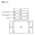
- FIG. 11 illustrates an example of a configuration of a light-emitting device in the case where analog video signals are input to a signal line driver circuit.
- the light-emitting device illustrated in FIG. 11 includes a pixel portion 600 which has a plurality of pixels, a scan line driver circuit 610 which controls a potential of a first scan line, a scan line driver circuit 620 which controls a potential of a second scan line, and a signal line driver circuit 630 which controls input of a video signal to a signal line.
- the signal line driver circuit 630 includes at least a shift register 631 , a sampling circuit 632 , and a memory circuit 633 which can store an analog signal.
- a clock signal S-CLK and a start pulse signal S-SP are input to the shift register 631 .
- the shift register 631 generates timing signals, pulses of which sequentially shift, in accordance with the clock signal S-CLK and the start pulse signal S-SP and inputs the timing signals to the sampling circuit 632 .
- the sampling circuit 632 samples analog video signals for one line period, which are input to the signal line driver circuit 630 , in accordance with the timing signals which are input.
- the sampled video signals are output to the memory circuit 633 all at once and held in accordance with a signal S-LS.
- the video signals held in the memory circuit 633 are input to the pixel portion 600 via signal lines.
- this embodiment mode describes an example in which after all the video signals for one line period are sampled in the sampling circuit 632 , the sampled video signals are input to the memory circuit 633 at the lower stage all at once, the present invention is not limited to this configuration. Every time each video signal for its respective pixel is sampled in the sampling circuit 632 , the sampled video signal can be input to the memory circuit 633 at the lower stage without waiting for the completion of the one line period.
- the video signals may be sampled for their respective pixels sequentially, or pixels in one line may be divided into several groups and the video signals for the pixels in one group may be sampled at the same time.
- the present invention is not limited to this configuration.
- a circuit which performs signal processing on the analog video signals output from the memory circuit 633 can be provided at the stage prior to the pixel portion 600 .
- Examples of the circuit which performs signal processing include a buffer which can shape a waveform and the like.
- the sampling circuit 632 can sample video signals for the next line period.
- Each of the scan line driver circuit 610 and the scan line driver circuit 620 includes circuits such as a shift register, a level shifter, and a buffer.
- the scan line driver circuit 610 and the scan line driver circuit 620 generate signals having the waveform illustrated in the timing chart in FIG. 4 or FIG. 8 . By inputting the generated signals to the first scan line or the second scan line, the operation of a switching element in each pixel is controlled.
- the scan line driver circuit 610 generates signals which are input to the first scan line and the scan line driver circuit 620 generates signals which are input to the second scan line; however, one scan line driver circuit may generate both signals which are input to the first scan line and signals which are input to the second scan line.
- one scan line driver circuit may generate both signals which are input to the first scan line and signals which are input to the second scan line.
- a plurality of the first scan lines and the second scan lines used for controlling the operation of the switching element be provided in each pixel, depending on the number of transistors and the polarity of each transistor included in the switching element.
- one scan line driver circuit may generate all signals that are input to the plurality of first scan lines, or a plurality of scan line driver circuits may generate signals that are input to the plurality of first scan lines. Further, one scan line driver circuit may generate all signals that are input to the plurality of second scan lines, or a plurality of scan line driver circuits may generate signals that are input to the plurality of second scan lines.
- the pixel portion 600 , the scan line driver circuit 610 , the scan line driver circuit 620 , and the signal line driver circuit 630 can be provided over the same substrate, any of them can be provided over a different substrate.
- grayscale can be displayed using an area ratio grayscale method or a time ratio grayscale method.
- An area ratio grayscale method refers to a driving method by which one pixel is divided into a plurality of sub-pixels and each sub-pixel is driven independently based on a video signal so that grayscale is displayed.
- a time ratio grayscale method refers to a driving method by which a period during which a pixel is in a light-emitting state is controlled so that grayscale is displayed.
- a light-emitting element Since the response speed of a light-emitting element is higher than that of a liquid crystal element or the like, a light-emitting element is more suitable for display using a time ratio grayscale method than a liquid crystal element.
- one frame period is divided into a plurality of sub-frame periods. Then, in accordance with a video signal, a light-emitting element in a pixel is set in a light-emitting state or a non-light-emitting state in each sub-frame period.
- a writing period and a display period are provided in each of all the sub-frame periods included in one frame period.
- at least one of all the sub-frame periods is provided with an erasing period in addition to the writing period and the display period.
- the writing period, the display period, and the erasing period may be provided in each of all the sub-frame periods.
- the length of each sub-frame period is shortened if the length of one frame period is fixed.
- an erasing period is sequentially started from a pixel in which the writing period is finished first and a display period is started so that the light-emitting element can be made not to emit light.
- This embodiment mode can be implemented in combination with any of the above embodiment modes and embodiments as appropriate.
- Light-emitting elements utilizing electroluminescence are classified according to whether a light-emitting material is an organic compound or an inorganic compound.
- a light-emitting material is an organic compound or an inorganic compound.
- the former is referred to as an organic light-emitting element, and the latter is referred to as an inorganic light-emitting element.
- an organic light-emitting element by application of a voltage to a pair of electrodes, electrons and holes are injected from the pair of electrodes into a layer including a light-emitting organic compound.
- the injected electron and hole form an exciton, and light (electroluminescence) is emitted when the electron and hole of the exciton are recombined at a given level.
- a recombination current flows through the light-emitting element. Owing to such a mechanism, this kind of light-emitting element is referred to as a current-excitation type light-emitting element.
- Inorganic light-emitting elements are classified into dispersion-type inorganic light-emitting elements and thin-film type inorganic light-emitting elements, depending on their element structures.
- the former include a semiconductor layer in which particles of a light-emitting material are dispersed in a binder, and the latter include a semiconductor layer formed of a thin film of a light-emitting material.
- As a light emission mechanism of inorganic light-emitting elements there are donor-acceptor recombination-type light emission that utilizes a donor level and an acceptor level and localized-type light emission that utilizes inner-shell electron transition of a metal ion.
- donor-acceptor recombination-type light emission is employed in dispersion type inorganic light-emitting elements and localized-type light emission is employed in thin-film type inorganic light-emitting elements in many cases.
- a thin-film type inorganic light-emitting element having a structure of a field-effect transistor will be described.
- light is emitted by applying a DC voltage between a pair of electrode layers which sandwich a semiconductor layer.
- a light-emitting transistor illustrated in FIG. 12A has, as well as an inverted-staggered structure, a bottom contact structure in which a semiconductor layer is formed over an electrode serving as a source (a source electrode) and an electrode serving as a drain (a drain electrode).
- an electrode 701 serving as a gate (a gate electrode 701 ) is formed over a substrate 700 having an insulating surface, and a gate insulating film 702 is formed over the gate electrode 701 .
- a source electrode 703 and a drain electrode 704 are formed so as to partly overlap with the gate electrode 701 with the gate insulating film 702 interposed therebetween.
- a semiconductor layer 705 is formed over the source electrode 703 , the drain electrode 704 , and the gate insulating film 702 .
- a current flows between the source electrode 703 and the drain electrode 704 of the light-emitting transistor, whereby the semiconductor layer 705 emits light.
- a light-emitting transistor having both a top contact structure in which a source electrode and a drain electrode are formed over a semiconductor layer and an inverted-staggered structure can be applied to the light-emitting device of the present invention.
- a gate electrode 701 is formed over a substrate 700 having an insulating surface, and a gate insulating film 702 is formed over the gate electrode 701 .
- a semiconductor layer 705 is formed so as to overlap with the gate electrode 701 with the gate insulating film 702 interposed therebetween, and a source electrode 703 and a drain electrode 704 are formed so as to partly cover the semiconductor layer 705 .
- each of the source electrode 703 and the drain electrode 704 is preferably formed so as to overlap with an end portion of the gate electrode 701 with the semiconductor layer 705 and the gate insulating film 702 interposed therebetween.
- a current flows between the source electrode 703 and the drain electrode 704 of the light-emitting transistor, whereby the semiconductor layer 705 emits light.
- a light-emitting transistor having a staggered structure can be applied to the light-emitting device of the present invention.
- a source electrode 703 and a drain electrode 704 are formed over a substrate 700 having an insulating surface, and a semiconductor layer 705 is formed over the source electrode 703 and the drain electrode 704 .
- a gate insulating film 702 is formed over the semiconductor layer 705 , the source electrode 703 , and the drain electrode 704 , and a gate electrode 701 is formed so as to overlap with the semiconductor layer 705 with the gate insulating film 702 interposed therebetween.
- the gate electrode 701 is preferably formed so as to overlap with an end portion of each of the source electrode 703 and the drain electrode 704 with the semiconductor layer 705 and the gate insulating film 702 interposed therebetween. A current flows between the source electrode 703 and the drain electrode 704 of the light-emitting transistor, whereby the semiconductor layer 705 emits light.
- a light-emitting transistor having a coplanar structure can be applied to the light-emitting device of the present invention.
- a semiconductor layer 705 is formed over a substrate 700 having an insulating surface, and a source electrode 703 and a drain electrode 704 are formed over the semiconductor layer 705 so as to partly overlap with the semiconductor layer 705 .
- a gate insulating film 702 is formed over the semiconductor layer 705 , the source electrode 703 , and the drain electrode 704 , and a gate electrode 701 is formed so as to overlap with the semiconductor layer 705 with the gate insulating film 702 interposed therebetween.
- the gate electrode 701 is preferably formed so as to overlap with an end portion of each of the source electrode 703 and the drain electrode 704 with the gate insulating film 702 interposed therebetween. A current flows between the source electrode 703 and the drain electrode 704 of the light-emitting transistor, whereby the semiconductor layer 705 emits light.
- a light-emitting transistor having an inverted-coplanar structure can be applied to the light-emitting device of the present invention.
- a gate electrode 701 , a source electrode 703 , and a drain electrode 704 are formed over a substrate 700 having an insulating surface, and a gate insulating film 702 is formed over the gate electrode 701 , the source electrode 703 , and the drain electrode 704 .
- a semiconductor layer 705 is formed so as to overlap with the gate electrode 701 , the source electrode 703 , and the drain electrode 704 with the gate insulating film 702 interposed therebetween.
- the semiconductor layer 705 is connected to the source electrode 703 and the drain electrode 704 through openings formed in the gate insulating film 702 .
- a current flows between the source electrode 703 and the drain electrode 704 of the light-emitting transistor, whereby the semiconductor layer 705 emits light.
- a light-emitting transistor having a coplanar structure which is different from that illustrated in FIG. 12D can be applied to the light-emitting device of the present invention.
- a semiconductor layer 705 is formed over a substrate 700 having an insulating surface, and a gate insulating film 702 is formed over the semiconductor layer 705 .
- a gate electrode 701 is formed so as to overlap with the semiconductor layer 705 with the gate insulating film 702 interposed therebetween.
- An interlayer insulating film 706 is formed over the gate electrode 701 and the gate insulating film 702 , and a source electrode 703 and a drain electrode 704 which are connected to the semiconductor layer 705 are formed over the interlayer insulating film 706 . Note that the source electrode 703 and the drain electrode 704 are connected to the semiconductor layer 705 through openings formed in the gate insulating film 702 and the interlayer insulating film 706 . A current flows between the source electrode 703 and the drain electrode 704 of the light-emitting transistor, whereby the semiconductor layer 705 emits light.
- a glass substrate, a quartz substrate, a sapphire substrate, a metal substrate or a stainless steel substrate each having a surface provided with an insulating layer, a plastic substrate having heat resistance that is high enough to resist the treatment temperature of the process, or the like can be used.
- a plastic substrate typically, a substrate including PET (polyethylene terephthalate), PEN (polyethylene naphthalate), PES (polyethersulfone), polypropylene, polypropylene sulfide, polycarbonate, polyetherimide, polyphenylene sulfide, polyphenylene oxide, polysulfone, polyphthalamide, or the like can be used.
- the light-emitting transistor of this embodiment can be formed by a method which does not require a high-temperature process, such as an evaporation method or a sputtering method. Accordingly, the light-emitting transistor can be formed directly on the plastic substrate.
- the light-emitting transistor may be formed after an insulating film is formed over a substrate.
- the insulating film can be formed using an insulating film including silicon oxide, silicon nitride, silicon oxynitride, silicon nitride oxide, aluminum nitride, or the like by a sputtering method, a plasma CVD method, a coating method, a printing method, or the like.
- the insulating film over the substrate can be a single layer or have a layered structure. The thickness of the insulating film is preferably 50 to 200 nm.
- a silicon oxynitride film means a film that includes more oxygen than nitrogen and, in the case where measurements are performed using Rutherford backscattering spectrometry (RBS) and hydrogen forward scattering (HFS), includes oxygen, nitrogen, silicon, and hydrogen at concentrations ranging from 50 to 70 at. %, 0.5 to 15 at. %, 25 to 35 at. %, and 0.1 to 10 at. %, respectively.
- a silicon nitride oxide film means a film that includes more nitrogen than oxygen and, in the case where measurements are performed using RBS and HFS, includes oxygen, nitrogen, silicon, and hydrogen at concentrations ranging from 5 to 30 at. %, 20 to 55 at. %, 25 to 35 at. %, and 10 to 25 at.
- the gate electrode 701 can be formed by a sputtering method, a plasma CVD method, a coating method, a printing method, an ink-jet method, an electrolytic plating method, an electroless plating method, or the like by using a conductive film formed of a metal, an alloy, a compound, or the like having conductivity with a single layer structure or a layered structure.
- a conductive metal oxide having a light-transmitting property such as indium tin oxide (hereinafter, referred to as ITO), indium tin oxide including silicon, or indium oxide including zinc oxide (ZnO) at 2 to 20 at. % is given.
- ITO indium tin oxide
- ZnO zinc oxide
- a nitride of the metal material e.g., titanium nitride, tungsten nitride, or molybdenum nitride
- a metal belonging to Group 1 or 2 of the periodic table i.e., an alkali metal such as lithium (Li) or cesium (Cs) or an alkaline earth metal such as magnesium (Mg), calcium (Ca), or strontium (Sr), aluminum (Al), an alloy including any of these (such as MgAg or AlLi), a rare earth metal such as europium (Er) or ytterbium (Yb), an alloy including the rare earth metal, or the like can be used.
- an alkali metal such as lithium (Li) or cesium (Cs) or an alkaline earth metal such as magnesium (Mg), calcium (Ca), or strontium (Sr), aluminum (Al), an alloy including any of these (such as MgAg or AlLi)
- a rare earth metal such as europium (Er) or ytterbium (Yb), an alloy including the rare earth metal, or the like
- Er europium
- Yb ytterbium
- the gate insulating film 702 has high withstand voltage and is a dense film. Further, the gate insulating film 702 preferably has a high dielectric constant.
- the gate insulating film 702 can be formed by a sputtering method, an evaporating method, a CVD method, a printing method, or the like.
- the source electrode 703 and the drain electrode 704 are preferably formed using a combination of a low-resistance material such as aluminum (Al) and a barrier metal using a high-melting-point metal material such as titanium (Ti) or molybdenum (Mo), e.g., a layered structure of titanium (Ti) and aluminum (Al) or a layered structure of molybdenum (Mo) and aluminum (Al).
- the source electrode 703 and the drain electrode 704 are not limited to the above structure and can be formed using a metal or a metal compound as appropriate.
- the source electrode 703 and the drain electrode 704 can be formed by a sputtering method, an evaporation method, a CVD method, a printing method, or the like.
- the source electrode 703 and the drain electrode 704 can be formed with the same material and the same layered structure as those of the gate electrode 701 .
- the semiconductor layer 705 is formed using a light-emitting material which includes a base material and an impurity element to be a luminescence center. Light emission of various colors can be obtained by varying impurity elements to be included in a light-emitting material.
- a method for manufacturing a light-emitting material various methods such as a solid phase method and a liquid phase method (a coprecipitation method) can be used.
- the solid phase method is a method in which a base material and an impurity element or a compound including the impurity element are weighed, mixed in a mortar, and reacted with each other by being heated and baked in an electric furnace so that the impurity element is made to be included in the base material.
- the baking temperature is preferably 700 to 1500° C. This is because solid phase reaction is not progressed at a temperature that is too low and the base material is decomposed at a temperature that is too high.
- the baking may be conducted in a powder state; however, the baking is preferably conducted in a pellet state. This method requires baking at a temperature that is comparatively high but is simple and, thus, this method has high productivity and is suitable for mass production.
- the liquid phase method is a method in which a base material or a compound including the base material and an impurity element or a compound including the impurity element are reacted with each other in a solution, dried, and then, baked.
- a base material or a compound including the base material and an impurity element or a compound including the impurity element are reacted with each other in a solution, dried, and then, baked.
- particles of a light-emitting material are uniformly dispersed, the particle has a small diameter, and reaction can progress even at low baking temperature.
- a sulfide As a base material for the light-emitting material, a sulfide, an oxide, a nitride, a carbide, or the like can be used.
- the sulfide can be, for example, zinc sulfide (ZnS), cadmium sulfide (CdS), calcium sulfide (CaS), yttrium sulfide (Y 2 S 3 ), gallium sulfide (Ga 2 S 3 ), strontium sulfide (SrS), barium sulfide (BaS), or the like.
- the oxide can be, for example, zinc oxide (ZnO), yttrium oxide (Y 2 O 3 ), Mg x Zn 1-x O, or the like.
- the nitride can be, for example, aluminum nitride (AlN), gallium nitride (GaN), indium nitride (InN), or the like.
- the carbide can be, for example, silicon carbide (SiC) or diamond.
- zinc selenide (ZnSe), zinc telluride (ZnTe), or the like can also be used.
- a ternary mixed crystal such as calcium gallium sulfide (CaGa 2 S 4 ), strontium-gallium sulfide (SrGa 2 S 4 ), or barium-gallium sulfide (BaGa 2 S 4 ) can also be used.
- manganese (Mn), copper (Cu), samarium (Sm), terbium (Tb), erbium (Er), thulium (Tm), europium (Eu), cerium (Ce), praseodymium (Pr), gold (Au), silver (Ag), or the like can be used.
- a halogen element such as fluorine (F) or chlorine (Cl) may be added.
- a light-emitting material including a first impurity element forming a donor level and a second impurity element forming an acceptor level can be used.
- the first impurity element for example, fluorine (F), chlorine (Cl), aluminum (Al), or the like can be used.
- the second impurity element for example, copper (Cu), silver (Ag), or the like can be used.
- the following steps are performed: weighing a base material, weighing a first impurity element or a compound including the first impurity element, weighing a second impurity element or a compound including the second impurity element, mixing them in a mortar, and heating and baking them in an electric furnace.
- the base material the base material as described above can be used, and as the first impurity element or the compound including the first impurity element, for example, fluorine (F), chlorine (Cl), aluminum sulfide (Al 2 S 3 ), or the like can be used.
- the second impurity element or the compound including the second impurity element for example, copper (Cu), silver (Ag), copper sulfide (Cu 2 S), silver sulfide (Ag 2 S), or the like can be used.
- the baking temperature is preferably 700 to 1500° C. This is because solid phase reaction is not progressed at a temperature that is too low and the base material is decomposed at a temperature that is too high.
- the baking may be conducted in a powder state; however, the baking is preferably conducted in a pellet state.
- a compound including a first impurity element and a second impurity element may also be used.
- the impurity elements are easily diffused to promote the solid phase reaction, a uniform light-emitting material can be obtained.
- the impurity element is not included excessively, a light-emitting material with high purity can be obtained.
- the compound including the first impurity element and the second impurity element for example, copper chloride (CuCl), silver chloride (AgCl), or the like can be given.
- concentration of these impurity elements may be 0.01 to 10 at. %, preferably 0.05 to 5 at. %, with respect to the base material.
- the semiconductor layer 705 can be formed using the above-mentioned light-emitting material, by a vacuum evaporation method such as a resistance heating evaporation method or an electron-beam evaporation (EB evaporation) method, a physical vapor deposition (PVD) method such as a sputtering method, a chemical vapor deposition (CVD) method such as a metal organic CVD method or a low-pressure hydride transport CVD method, an atomic layer epitaxy (ALE) method, or the like.
- a vacuum evaporation method such as a resistance heating evaporation method or an electron-beam evaporation (EB evaporation) method
- PVD physical vapor deposition
- CVD chemical vapor deposition
- ALE atomic layer epitaxy
- the semiconductor layer 705 may also be formed in such a manner that a film including the light-emitting material is formed over a substrate by any of the above methods, and then the film including the light-emitting material is selectively etched using a resist mask formed through a photolithography process.
- a dry etching method, a wet etching method, or the like can be used.
- a mixed gas of CF 4 and O 2 a mixed gas of BCl 3 and Cl 2 , Cl 2 , or the like can be used as an etching gas.
- a light-blocking material is used for the gate electrode 701
- a material with a lower refractive index than that of the semiconductor layer 705 is used for the gate insulating film 702 , whereby light generated in the semiconductor layer 705 is reflected at the interface between the semiconductor layer 705 and the gate insulating film 702 . Accordingly, emitted light can be efficiently extracted to the side opposite to the substrate 700 .
- a light-transmitting material is used for the gate electrode 701 , and a material with a higher refractive index than that of the semiconductor layer 705 is used for the gate insulating film 702 , whereby light generated in the semiconductor layer 705 can be extracted in two directions, i.e., the substrate 700 side and the side opposite to the substrate 700 . Accordingly, a light-emitting device capable of dual-emission can be manufactured.
- a material with a refractive index lower than 2 may be used for forming the gate insulating film 702 in the case of a light-emitting transistor having a structure in which light emitted is extracted to the side opposite to the substrate 700 .
- Examples of such a material for the gate insulating film 702 include silicon oxide (SiO 2 ), hafnium oxide (HfO 2 ), aluminum oxide (Al 2 O 3 ), and the like.
- a material with a refractive index higher than 2 may be used for forming the gate insulating film 702 .
- Examples of such a material for the gate insulating film 702 include silicon nitride (SiN), barium titanate (BaTiO 3 ), titanium oxide (TiO 2 ), zirconium oxide (ZrO 2 ), tantalum oxide (Ta 2 O 5 ), niobium oxide (Nb 2 O 5 ), and the like.
- the interlayer insulating film 706 can be formed to have a single layer structure or a layered structure, using an insulating film including an inorganic compound such as silicon oxide, silicon nitride, silicon oxynitride, or silicon nitride oxide by a sputtering method, a plasma CVD method, a coating method, a printing method, or the like.
- the interlayer insulating film 706 can be formed using polyimide, acrylic, or a siloxane polymer.
- the light-emitting transistor described in this embodiment has a field-effect transistor structure, so that a large number of carriers can be injected to the semiconductor layer. Therefore, in the case where a light-emitting material that is an inorganic compound is used for the semiconductor layer 705 , the light-emitting efficiency can be increased and the driving voltage can be reduced, compared to a light-emitting element having a simple layered structure. Further, by providing the light-emitting transistor in a pixel portion, the driving voltage of a light-emitting device can be reduced.
- the polarity of a light-emitting transistor using an inorganic compound as a light-emitting material depends on the polarity of the semiconductor layer 705 .
- a light-emitting material for the semiconductor layer 705 it is possible to form either an n-channel light-emitting transistor or a p-channel light-emitting transistor.
- zinc oxide (ZnO), Mg x Zn 1-x O, zinc sulfide (ZnS), or cadmium sulfide (CdS) for the base material of the semiconductor layer 705
- an n-channel light-emitting transistor can be formed.
- zinc telluride (ZnTe) zinc telluride
- a p-channel light-emitting transistor can be formed.
- the structure of the inorganic light-emitting transistor is described.
- an organic light-emitting transistor can also be applied to the light-emitting device of the present invention.
- the organic light-emitting transistor can be formed by using an organic semiconductor for the semiconductor layer 705 .
- any of a low molecular compound, an intermolecular compound (that is not sublimable and has a molecular chain length less than or equal to 10 ⁇ m), and a high molecular compound can be used as long as it is an organic material which has a carrier-transporting property and can cause modulation in the carrier density by an electric field effect.
- an organic semiconductor for forming a p-channel organic light-emitting transistor the following compounds can be used.
- a low molecular compound a polycyclic aromatic compound such as pentacene or naphthacene, a conjugated double bond compound, a macrocycle compound or a complex thereof, phthalocyanine, a charge transfer type complex, or a tetrathiafulvalene-tetracyanoquinodimethane complex can be used.
- a ⁇ -conjugated polymer a charge transfer type complex, polyvinyl pyridine, a phthalocyanine metal complex, or the like can be used.
- polyacetylene, polyaniline, polypyrrole, polythienylene, a polythiophene derivative, or the like which is a ⁇ -conjugated polymer constituted by a conjugated double bond can be used.
- perylenetetracarboxylic acid anhydride or a derivative thereof perylenetetracarboxydiimie derivative, naphthalenetetracarboxylic acid anhydride or a derivative thereof, a naphthalenetetracarboxydiimide derivative, a metallophthalocyanine derivative, fullerene, or the like, can be used.
- the semiconductor layer 705 using the organic semiconductor described above can be formed by a known method such as an evaporation method, a spin-coating method, a dipping method, a silkscreen method, a spray method, or a droplet discharge method.
- the following materials can be used: a metal such as platinum (Pt), gold (Au), aluminum (Al), chromium (Cr), nickel (Ni), cobalt (Co), copper (Cu), titanium (Ti), magnesium (Mg), calcium (Ca), barium (Ba), or sodium (Na); an alloy including any of the metals; a conductive high molecular compound such as polyaniline, polypyrrole, polythiophene, polyacetylene, or polydiacetylene; an inorganic semiconductor such as silicon, germanium, or gallium arsenide; a carbon material such as carbon black, fullerene, carbon nanotube, or graphite; the conductive high molecular compound, the inorganic semiconductor, or the carbon material doped with acid (including Lewis acid), a halogen atom, or a metal atom of an alkali metal, an alkaline earth metal, or the like; and the like
- the gate insulating film 702 of the organic light-emitting transistor can be formed using an organic insulating material such as acrylic or polyimide or a siloxane based material, in addition to the inorganic insulating material.
- an organic insulating material such as acrylic or polyimide or a siloxane based material
- siloxane a skeleton structure is formed of a bond of silicon and oxygen, and a compound at least including hydrogen (such as an alkyl group or aromatic hydrocarbon) is used as a substituent.
- Fluorine may also be used as a substituent.
- fluorine and a compound at least including hydrogen may be used as a substituent.
- the gate insulating film 702 may be formed using a single layer or a plurality of layers.
- an inorganic insulating material as a first insulating layer and an organic insulating material as a second insulating layer are preferably stacked.
- the gate insulating film 702 using an organic material or a siloxane based material can be formed by a coating method.
- the polarity (p-type or n-type) of the light-emitting transistor using the organic semiconductor depends on not only a material for the organic semiconductor but also a relation of work functions of the organic semiconductor and the source and drain electrodes which inject carriers. Therefore, the organic light-emitting transistor can be p-type, n-type, or bipolar regardless of the material for the organic semiconductor. In order to select the polarity (p-type or n-type) of the organic light-emitting transistor, it is necessary to consider the relation of work functions of the organic semiconductor and the source and drain electrodes, and the intensity of an electric field for carrier injection, in addition to selection of the appropriate material for the organic semiconductor.
- This embodiment can be implemented in combination with any of the above embodiment modes as appropriate.
- FIG. 14A is a top view of a pixel of this embodiment.
- FIG. 14B is a circuit diagram of the pixel illustrated in FIG. 14A .
- FIG. 15 is a cross-sectional view taken along dashed line A-A′ in the top view of FIG. 14A .
- FIG. 14B is a circuit diagram in the case where transistors are used for the first switching element 302 and the second switching element 303 of the pixel illustrated in FIG. 6A .
- a gate of a transistor 801 used as the first switching element is connected to a first scan line Gaj.
- one of a source and a drain of the transistor 801 is connected to a signal line Si and the other of the source and the drain is connected to a gate of a light-emitting transistor 802 .
- a gate of a transistor 803 used as the second switching element is connected to a second scan line Gbj.
- the gate of the light-emitting transistor 802 is connected to one of a source and a drain of the transistor 803 , and a common potential is applied to the other of the source and the drain of the transistor 803 .
- a storage capacitor 804 is provided so as to hold the potential of the gate of the light-emitting transistor 802 .
- the gate of the light-emitting transistor 802 is connected to one of a pair of electrodes of the storage capacitor 804 , and the common potential is applied to the other of the pair of electrodes of the storage capacitor 804 .
- the transistor 801 includes a conductive film 811 formed over an insulating surface, an insulating film 812 formed over the conductive film 811 , a semiconductor layer 813 which overlaps with the conductive film 811 with the insulating film 812 interposed therebetween, and conductive films 814 and 815 formed so as to partly overlap with the semiconductor layer 813 .
- the conductive film 811 serves as the gate of the transistor 801 .
- the conductive film 811 and conductive films 816 and 819 can be formed by processing (patterning) a conductive film formed over the insulating surface into desired shapes.
- One of the conductive films 814 and 815 serves as the source of the transistor 801 , and the other of the conductive films 814 and 815 serves as the drain of the transistor 801 .
- the conductive films 814 and 815 and a conductive film 818 can be formed by processing (patterning) a conductive film formed over the insulating film 812 into desired shapes.
- the insulating film 812 serves as a gate insulating film of the transistor 801 .
- the transistor 803 includes the conductive film 816 formed over the insulating surface, the insulating film 812 formed over the conductive film 816 , a semiconductor layer 817 which overlaps with the conductive film 816 with the insulating film 812 interposed therebetween, and the conductive films 815 and 818 formed so as to partly overlap with the semiconductor layer 817 .
- the conductive film 816 serves as the gate of the transistor 803 .
- One of the conductive films 815 and 818 serves as the source of the transistor 803 , and the other of the conductive films 815 and 818 serves as the drain of the transistor 803 .
- the insulating film 812 serves as a gate insulating film of the transistor 803 .
- the storage capacitor 804 includes the conductive film 819 formed over the insulating surface, the insulating film 812 formed over the conductive film 819 , and the conductive film 818 formed so as to overlap with the conductive film 819 with the insulating film 812 interposed therebetween.
- the conductive films 819 and 818 serve as the pair of electrodes of the storage capacitor 804 .
- the conductive film 819 is connected to the conductive film 815 through an opening formed in the insulating film 812 .
- An interlayer insulating film 820 is formed so as to cover the transistors 801 and 803 and the storage capacitor 804 .
- FIG. 14A and FIG. 15 illustrate an example of the light-emitting transistor 802 having an inverted-staggered structure illustrated in FIG. 12B
- the light-emitting transistor 802 includes a conductive film 821 formed over the interlayer insulating film 820 , an insulating film 822 formed over the conductive film 821 , conductive films 823 and 824 formed so as to partly overlap with the conductive film 821 with the insulating film 822 interposed therebetween, and a semiconductor layer 825 formed so as to overlap with the conductive film 821 with the insulating film 822 interposed therebetween.
- the semiconductor layer 825 is connected to the conductive films 823 and 824 .
- the conductive film 821 serves as the gate of the light-emitting transistor 802 .
- One of the conductive films 823 and 824 serves as a source of the light-emitting transistor 802 and the other of the conductive films 823 and 824 serves as a drain of the light-emitting transistor 803 .
- the insulating film 822 serves as a gate insulating film of the light-emitting transistor 802 .
- the conductive film 821 is connected to the conductive film 815 through an opening formed in the interlayer insulating film 820 .
- the conductive film 823 is connected to the conductive film 818 through an opening formed in the insulating film 822 and the interlayer insulating film 820 .
- the conductive film 811 serves as the first scan line Gaj, and the conductive film 816 serves as the second scan line Gbj.
- the conductive film 814 serves as the signal line Si, and the conductive film 818 serves as a wiring for supplying the common potential to the light-emitting transistor 802 .
- the conductive film 824 serves as a power supply line Vi.
- This embodiment can be implemented in combination with any of the above embodiment modes and embodiment as appropriate.
- FIGS. 16A and 16B are perspective views each illustrating a light-emitting device obtained by mounting an IC with a chip shape (IC chip) on a panel.
- a pixel portion 6002 and a scan line driver circuit 6003 are formed between a substrate 6001 and a substrate 6006 .
- An IC chip 6004 having a signal line driver circuit is mounted on the substrate 6001 .
- the IC chip 6004 having the signal line driver circuit is attached to the substrate 6001 and electrically connected to the pixel portion 6002 .
- Reference numeral 6005 denotes an FPC. Electric power, various signals, and the like are supplied to the pixel portion 6002 , the scan line driver circuit 6003 , and the signal line driver circuit via the FPC 6005 .
- a pixel portion 6102 and a scan line driver circuit 6103 are formed between a substrate 6101 and a substrate 6106 .
- an IC chip 6104 having a signal line driver circuit is mounted on an FPC 6105 which is mounted on the substrate 6101 . Electric power, various signals, and the like are supplied to the pixel portion 6102 , the scan line driver circuit 6103 , and the signal line driver circuit via the FPC 6105 .
- FIGS. 16A and 16B each illustrate the example in which the IC chip has only the signal line driver circuit, the IC chip may have the scan line driver circuit.
- the IC chip having a controller, a CPU, a memory, or the like may be mounted. Further, the IC chip does not necessarily have an entire signal line driver circuit or scan line driver circuit but the IC chip may have only part of each driver circuit.
- the yield can be improved and optimization of a process according to characteristics of each circuit can be easily performed, compared to the case of forming all circuits over the same substrate as the pixel portion.
- This embodiment can be implemented in combination with any of the above embodiment modes and embodiments.
- the present invention can provide a light-emitting device which can suppress power consumption and prevent a blur of a moving image. Therefore, the light-emitting device of the present invention is preferably used for display devices, laptop personal computers, or image reproducing devices provided with a recording medium (typically, a device which can reproduce a recording medium such as a DVD (digital versatile disc) and which has a display capable of displaying the image).
- a recording medium typically, a device which can reproduce a recording medium such as a DVD (digital versatile disc) and which has a display capable of displaying the image.
- examples of an electronic device which can use the light-emitting device of the present invention include cellular phones, portable game machines, electronic book readers, cameras such as video cameras and digital still cameras, goggle type displays (head mounted displays), navigation systems, audio reproducing devices (e.g., car audio components and audio components), and the like.
- FIGS. 17A to 17C illustrate specific examples of these electronic devices.
- FIG. 17A illustrates a display device including a housing 5001 , a display portion 5002 , speaker portions 5003 , and the like.
- the light-emitting device of the present invention can be used for the display portion 5002 .
- the display device includes all display devices for displaying information, for example, for a personal computer, for receiving TV broadcasting, and for displaying an advertisement.
- FIG. 17B illustrates a laptop personal computer including a main body 5201 , a housing 5202 , a display portion 5203 , a keyboard 5204 , a pointing device 5205 , and the like.
- the light-emitting device of the present invention can be used for the display portion 5203 .
- FIG. 17C illustrates a potable image reproducing device provided with a recording medium (specifically a DVD player), which includes a main body 5401 , a housing 5402 , a display portion 5403 , a recording medium (DVD or the like) reading portion 5404 , operation keys 5405 , speaker portions 5406 , and the like.
- the image reproducing device provided with a recording medium includes a home-use game machine and the like.
- the light-emitting device of the present invention can be used for the display portion 5403 .
- the application range of the present invention is very wide and the present invention can be applied to electronic devices in various fields.
- This embodiment can be implemented in combination with any of the above embodiment modes and embodiments as appropriate.
Abstract
Description
Claims (6)
Applications Claiming Priority (2)
| Application Number | Priority Date | Filing Date | Title |
|---|---|---|---|
| JP2008017188 | 2008-01-29 | ||
| JP2008-017188 | 2008-01-29 |
Publications (2)
| Publication Number | Publication Date |
|---|---|
| US20090189161A1 US20090189161A1 (en) | 2009-07-30 |
| US8022406B2 true US8022406B2 (en) | 2011-09-20 |
Family
ID=40380594
Family Applications (1)
| Application Number | Title | Priority Date | Filing Date |
|---|---|---|---|
| US12/358,843 Expired - Fee Related US8022406B2 (en) | 2008-01-29 | 2009-01-23 | Light emitting device |
Country Status (3)
| Country | Link |
|---|---|
| US (1) | US8022406B2 (en) |
| EP (1) | EP2085958B1 (en) |
| JP (1) | JP5386182B2 (en) |
Families Citing this family (9)
| Publication number | Priority date | Publication date | Assignee | Title |
|---|---|---|---|---|
| JP2016139560A (en) * | 2015-01-28 | 2016-08-04 | 株式会社ジャパンディスプレイ | Display device |
| JP6546400B2 (en) * | 2015-02-05 | 2019-07-17 | 株式会社ジャパンディスプレイ | Display device |
| CN105869574B (en) * | 2016-06-07 | 2017-03-29 | 京东方科技集团股份有限公司 | A kind of pixel-driving circuit and its driving method, array base palte and display device |
| JP6844845B2 (en) | 2017-05-31 | 2021-03-17 | 三国電子有限会社 | Display device |
| JP7190729B2 (en) * | 2018-08-31 | 2022-12-16 | 三国電子有限会社 | ORGANIC ELECTROLUMINESCENT DEVICE HAVING CARRIER INJECTION CONTROL ELECTRODE |
| JP7246681B2 (en) | 2018-09-26 | 2023-03-28 | 三国電子有限会社 | TRANSISTOR, TRANSISTOR MANUFACTURING METHOD, AND DISPLAY DEVICE INCLUDING TRANSISTOR |
| JP7190740B2 (en) | 2019-02-22 | 2022-12-16 | 三国電子有限会社 | Display device having an electroluminescence element |
| JPWO2020226045A1 (en) * | 2019-05-09 | 2020-11-12 | ||
| JP7444436B2 (en) | 2020-02-05 | 2024-03-06 | 三国電子有限会社 | liquid crystal display device |
Citations (18)
| Publication number | Priority date | Publication date | Assignee | Title |
|---|---|---|---|---|
| EP1061497A1 (en) | 1999-06-17 | 2000-12-20 | Sony Corporation | Image display apparatus including current controlled light emitting elements and driving method therefor |
| EP1103946A2 (en) | 1999-11-29 | 2001-05-30 | Sel Semiconductor Energy Laboratory Co., Ltd. | Gradation control for an active matrix EL display |
| JP2002151276A (en) | 2000-08-10 | 2002-05-24 | Semiconductor Energy Lab Co Ltd | Display device and electronic equipment |
| US20030111966A1 (en) | 2001-12-19 | 2003-06-19 | Yoshiro Mikami | Image display apparatus |
| US20030142509A1 (en) | 2001-12-28 | 2003-07-31 | Hiroshi Tsuchiya | Intermittently light emitting display apparatus |
| WO2003071608A1 (en) | 2002-02-19 | 2003-08-28 | Hoya Corporation | Light-emitting device of field-effect transistor type |
| US20030218166A1 (en) | 2002-05-21 | 2003-11-27 | Semiconductor Energy Laboratory Co., Ltd. | Organic field effect transistor |
| US6730966B2 (en) | 1999-11-30 | 2004-05-04 | Semiconductor Energy Laboratory Co., Ltd. | EL display using a semiconductor thin film transistor |
| US6825820B2 (en) | 2000-08-10 | 2004-11-30 | Semiconductor Energy Laboratory Co., Ltd. | Display device and electronic device |
| US20060103290A1 (en) * | 2004-11-17 | 2006-05-18 | Suh Min-Chul | Organic electroluminescence device and method of manufacturing the same |
| JP2006253163A (en) | 2005-03-07 | 2006-09-21 | Ricoh Co Ltd | Organic transistor and display |
| US20060208962A1 (en) | 2005-03-07 | 2006-09-21 | Takuro Sekiya | Organic transistor, organic transistor unit and display device |
| JP2006253162A (en) | 2005-03-07 | 2006-09-21 | Ricoh Co Ltd | Organic transistor and display |
| JP2006252775A (en) | 2005-03-07 | 2006-09-21 | Ricoh Co Ltd | Display device |
| JP2006253164A (en) | 2005-03-07 | 2006-09-21 | Ricoh Co Ltd | Organic transistor and display |
| JP2006252774A (en) | 2005-03-07 | 2006-09-21 | Ricoh Co Ltd | Organic transistor and display device |
| WO2007043697A1 (en) | 2005-10-14 | 2007-04-19 | Pioneer Corporation | Light emitting device and display device |
| WO2007063992A1 (en) | 2005-12-02 | 2007-06-07 | Dai Nippon Printing Co., Ltd. | Organic light emitting transistor element and method for manufacturing same |
Family Cites Families (5)
| Publication number | Priority date | Publication date | Assignee | Title |
|---|---|---|---|---|
| JP3686769B2 (en) * | 1999-01-29 | 2005-08-24 | 日本電気株式会社 | Organic EL element driving apparatus and driving method |
| JP4906106B2 (en) * | 2003-07-14 | 2012-03-28 | 株式会社半導体エネルギー研究所 | Light emitting device |
| JP4972727B2 (en) * | 2005-07-20 | 2012-07-11 | 日本電信電話株式会社 | ORGANIC SEMICONDUCTOR LIGHT EMITTING ELEMENT, DISPLAY DEVICE USING SAME, AND METHOD FOR MANUFACTURING ORGANIC SEMICONDUCTOR LIGHT EMITTING ELEMENT |
| WO2007043696A1 (en) | 2005-10-14 | 2007-04-19 | Pioneer Corporation | Thin film semiconductor device and display |
| JP2009009781A (en) * | 2007-06-27 | 2009-01-15 | Semiconductor Energy Lab Co Ltd | Light-emitting device and electronic equipment |
-
2009
- 2009-01-21 EP EP09000812A patent/EP2085958B1/en not_active Not-in-force
- 2009-01-21 JP JP2009010545A patent/JP5386182B2/en not_active Expired - Fee Related
- 2009-01-23 US US12/358,843 patent/US8022406B2/en not_active Expired - Fee Related
Patent Citations (28)
| Publication number | Priority date | Publication date | Assignee | Title |
|---|---|---|---|---|
| US6583775B1 (en) | 1999-06-17 | 2003-06-24 | Sony Corporation | Image display apparatus |
| EP1061497A1 (en) | 1999-06-17 | 2000-12-20 | Sony Corporation | Image display apparatus including current controlled light emitting elements and driving method therefor |
| US7113154B1 (en) | 1999-11-29 | 2006-09-26 | Semiconductor Energy Laboratory Co., Ltd. | Electronic device |
| EP1103946A2 (en) | 1999-11-29 | 2001-05-30 | Sel Semiconductor Energy Laboratory Co., Ltd. | Gradation control for an active matrix EL display |
| JP2001343933A (en) | 1999-11-29 | 2001-12-14 | Semiconductor Energy Lab Co Ltd | Light emission device |
| US6982462B2 (en) | 1999-11-30 | 2006-01-03 | Semiconductor Energy Laboratory Co., Ltd. | Light emitting display device using multi-gate thin film transistor |
| US20060033161A1 (en) | 1999-11-30 | 2006-02-16 | Semiconductor Energy Laboratory Co., Ltd. | Electric device |
| US6730966B2 (en) | 1999-11-30 | 2004-05-04 | Semiconductor Energy Laboratory Co., Ltd. | EL display using a semiconductor thin film transistor |
| JP2002151276A (en) | 2000-08-10 | 2002-05-24 | Semiconductor Energy Lab Co Ltd | Display device and electronic equipment |
| US6825820B2 (en) | 2000-08-10 | 2004-11-30 | Semiconductor Energy Laboratory Co., Ltd. | Display device and electronic device |
| US20050093802A1 (en) | 2000-08-10 | 2005-05-05 | Semiconductor Energy Laboratory Co., Ltd. | Display device and electronic device |
| US20030111966A1 (en) | 2001-12-19 | 2003-06-19 | Yoshiro Mikami | Image display apparatus |
| US20030142509A1 (en) | 2001-12-28 | 2003-07-31 | Hiroshi Tsuchiya | Intermittently light emitting display apparatus |
| WO2003071608A1 (en) | 2002-02-19 | 2003-08-28 | Hoya Corporation | Light-emitting device of field-effect transistor type |
| US20060043380A1 (en) | 2002-02-19 | 2006-03-02 | Kawazoe Hiroshi | Light-emitting device of field-effect transistor type |
| EP1478031A1 (en) | 2002-02-19 | 2004-11-17 | Hoya Corporation | Light-emitting device of field-effect transistor type |
| US20030218166A1 (en) | 2002-05-21 | 2003-11-27 | Semiconductor Energy Laboratory Co., Ltd. | Organic field effect transistor |
| US20060103290A1 (en) * | 2004-11-17 | 2006-05-18 | Suh Min-Chul | Organic electroluminescence device and method of manufacturing the same |
| JP2006253163A (en) | 2005-03-07 | 2006-09-21 | Ricoh Co Ltd | Organic transistor and display |
| JP2006253162A (en) | 2005-03-07 | 2006-09-21 | Ricoh Co Ltd | Organic transistor and display |
| JP2006252775A (en) | 2005-03-07 | 2006-09-21 | Ricoh Co Ltd | Display device |
| JP2006253164A (en) | 2005-03-07 | 2006-09-21 | Ricoh Co Ltd | Organic transistor and display |
| JP2006252774A (en) | 2005-03-07 | 2006-09-21 | Ricoh Co Ltd | Organic transistor and display device |
| US20060208962A1 (en) | 2005-03-07 | 2006-09-21 | Takuro Sekiya | Organic transistor, organic transistor unit and display device |
| WO2007043697A1 (en) | 2005-10-14 | 2007-04-19 | Pioneer Corporation | Light emitting device and display device |
| US20090135105A1 (en) | 2005-10-14 | 2009-05-28 | Pioneer Corporation | Light-emitting element and display apparatus using the same |
| WO2007063992A1 (en) | 2005-12-02 | 2007-06-07 | Dai Nippon Printing Co., Ltd. | Organic light emitting transistor element and method for manufacturing same |
| US20090179195A1 (en) | 2005-12-02 | 2009-07-16 | Dai Nippon Printing Co., Ltd. | Organic Luminescence Transistor Device and Manufacturing Method Thereof |
Non-Patent Citations (2)
| Title |
|---|
| European Search report re application No. EP 09000812.9, dated Mar. 16, 2010. |
| Inukai, K. et al, "36.4L: Late-News Paper: 4.0-in. TFT-OLED Displays and a Novel Digital Driving Method," SID Digest '00, SID International Symposium Digest of Technical Papers, vol. 31, 2000, pp. 924-927. |
Also Published As
| Publication number | Publication date |
|---|---|
| JP5386182B2 (en) | 2014-01-15 |
| EP2085958A2 (en) | 2009-08-05 |
| US20090189161A1 (en) | 2009-07-30 |
| EP2085958B1 (en) | 2012-08-01 |
| JP2009206505A (en) | 2009-09-10 |
| EP2085958A3 (en) | 2010-04-14 |
Similar Documents
| Publication | Publication Date | Title |
|---|---|---|
| JP7400130B2 (en) | display device | |
| US8022406B2 (en) | Light emitting device | |
| JP2023134470A (en) | Display | |
| TWI407569B (en) | Semiconductor device, display device, and electronic device | |
| JP5508664B2 (en) | Semiconductor device, display device and electronic apparatus | |
| KR101187398B1 (en) | Display device and driving method of the same | |
| JP4522777B2 (en) | Method for manufacturing light emitting device |
Legal Events
| Date | Code | Title | Description |
|---|---|---|---|
| AS | Assignment |
Owner name: SEMICONDUCTOR ENERGY LABORATORY CO., LTD., JAPAN Free format text: ASSIGNMENT OF ASSIGNORS INTEREST;ASSIGNOR:HONDA, TATSUYA;REEL/FRAME:022149/0238 Effective date: 20090119 |
|
| ZAAA | Notice of allowance and fees due |
Free format text: ORIGINAL CODE: NOA |
|
| ZAAB | Notice of allowance mailed |
Free format text: ORIGINAL CODE: MN/=. |
|
| STCF | Information on status: patent grant |
Free format text: PATENTED CASE |
|
| FEPP | Fee payment procedure |
Free format text: PAYOR NUMBER ASSIGNED (ORIGINAL EVENT CODE: ASPN); ENTITY STATUS OF PATENT OWNER: LARGE ENTITY |
|
| FPAY | Fee payment |
Year of fee payment: 4 |
|
| MAFP | Maintenance fee payment |
Free format text: PAYMENT OF MAINTENANCE FEE, 8TH YEAR, LARGE ENTITY (ORIGINAL EVENT CODE: M1552); ENTITY STATUS OF PATENT OWNER: LARGE ENTITY Year of fee payment: 8 |
|
| FEPP | Fee payment procedure |
Free format text: MAINTENANCE FEE REMINDER MAILED (ORIGINAL EVENT CODE: REM.); ENTITY STATUS OF PATENT OWNER: LARGE ENTITY |
|
| LAPS | Lapse for failure to pay maintenance fees |
Free format text: PATENT EXPIRED FOR FAILURE TO PAY MAINTENANCE FEES (ORIGINAL EVENT CODE: EXP.); ENTITY STATUS OF PATENT OWNER: LARGE ENTITY |
|
| STCH | Information on status: patent discontinuation |
Free format text: PATENT EXPIRED DUE TO NONPAYMENT OF MAINTENANCE FEES UNDER 37 CFR 1.362 |
|
| FP | Lapsed due to failure to pay maintenance fee |
Effective date: 20230920 |