US8026762B2 - High efficiency transmitter for wireless communication - Google Patents
High efficiency transmitter for wireless communication Download PDFInfo
- Publication number
- US8026762B2 US8026762B2 US12/487,206 US48720609A US8026762B2 US 8026762 B2 US8026762 B2 US 8026762B2 US 48720609 A US48720609 A US 48720609A US 8026762 B2 US8026762 B2 US 8026762B2
- Authority
- US
- United States
- Prior art keywords
- distortion
- constant envelope
- envelope signals
- phase
- linear
- Prior art date
- Legal status (The legal status is an assumption and is not a legal conclusion. Google has not performed a legal analysis and makes no representation as to the accuracy of the status listed.)
- Expired - Fee Related
Links
- 238000004891 communication Methods 0.000 title description 6
- 238000012937 correction Methods 0.000 claims abstract description 24
- 230000006870 function Effects 0.000 claims description 26
- 238000000034 method Methods 0.000 claims description 16
- 239000013598 vector Substances 0.000 claims description 14
- 238000001914 filtration Methods 0.000 claims description 11
- 230000006735 deficit Effects 0.000 claims description 6
- 238000013442 quality metrics Methods 0.000 claims description 3
- 238000000354 decomposition reaction Methods 0.000 description 10
- 230000005540 biological transmission Effects 0.000 description 9
- 238000004088 simulation Methods 0.000 description 9
- 230000008901 benefit Effects 0.000 description 7
- 238000005070 sampling Methods 0.000 description 7
- 238000012545 processing Methods 0.000 description 6
- 230000003321 amplification Effects 0.000 description 4
- 238000006243 chemical reaction Methods 0.000 description 4
- 230000001934 delay Effects 0.000 description 4
- 230000003111 delayed effect Effects 0.000 description 4
- 230000000694 effects Effects 0.000 description 4
- 230000015654 memory Effects 0.000 description 4
- 238000003199 nucleic acid amplification method Methods 0.000 description 4
- 238000013459 approach Methods 0.000 description 3
- 230000007423 decrease Effects 0.000 description 3
- 230000015556 catabolic process Effects 0.000 description 2
- 238000006731 degradation reaction Methods 0.000 description 2
- 238000013461 design Methods 0.000 description 2
- 238000011161 development Methods 0.000 description 2
- 238000003780 insertion Methods 0.000 description 2
- 230000037431 insertion Effects 0.000 description 2
- 238000007620 mathematical function Methods 0.000 description 2
- 238000012986 modification Methods 0.000 description 2
- 230000004048 modification Effects 0.000 description 2
- 230000003287 optical effect Effects 0.000 description 2
- 230000010363 phase shift Effects 0.000 description 2
- 230000008569 process Effects 0.000 description 2
- 230000009467 reduction Effects 0.000 description 2
- 230000004044 response Effects 0.000 description 2
- 230000009471 action Effects 0.000 description 1
- 230000003044 adaptive effect Effects 0.000 description 1
- 238000004378 air conditioning Methods 0.000 description 1
- 230000008859 change Effects 0.000 description 1
- 239000002131 composite material Substances 0.000 description 1
- 230000003750 conditioning effect Effects 0.000 description 1
- 238000010276 construction Methods 0.000 description 1
- 230000001419 dependent effect Effects 0.000 description 1
- 238000001514 detection method Methods 0.000 description 1
- 238000005265 energy consumption Methods 0.000 description 1
- 239000000463 material Substances 0.000 description 1
- 239000011159 matrix material Substances 0.000 description 1
- 238000005259 measurement Methods 0.000 description 1
- 239000013307 optical fiber Substances 0.000 description 1
- 230000001151 other effect Effects 0.000 description 1
- 230000035945 sensitivity Effects 0.000 description 1
- 238000000926 separation method Methods 0.000 description 1
- 238000005549 size reduction Methods 0.000 description 1
- 239000007787 solid Substances 0.000 description 1
- 239000000126 substance Substances 0.000 description 1
- 230000001629 suppression Effects 0.000 description 1
- 239000013585 weight reducing agent Substances 0.000 description 1
Images


Classifications
-
- H—ELECTRICITY
- H03—ELECTRONIC CIRCUITRY
- H03F—AMPLIFIERS
- H03F1/00—Details of amplifiers with only discharge tubes, only semiconductor devices or only unspecified devices as amplifying elements
- H03F1/02—Modifications of amplifiers to raise the efficiency, e.g. gliding Class A stages, use of an auxiliary oscillation
- H03F1/0205—Modifications of amplifiers to raise the efficiency, e.g. gliding Class A stages, use of an auxiliary oscillation in transistor amplifiers
- H03F1/0294—Modifications of amplifiers to raise the efficiency, e.g. gliding Class A stages, use of an auxiliary oscillation in transistor amplifiers using vector summing of two or more constant amplitude phase-modulated signals
-
- H—ELECTRICITY
- H03—ELECTRONIC CIRCUITRY
- H03F—AMPLIFIERS
- H03F1/00—Details of amplifiers with only discharge tubes, only semiconductor devices or only unspecified devices as amplifying elements
- H03F1/32—Modifications of amplifiers to reduce non-linear distortion
-
- H—ELECTRICITY
- H03—ELECTRONIC CIRCUITRY
- H03F—AMPLIFIERS
- H03F1/00—Details of amplifiers with only discharge tubes, only semiconductor devices or only unspecified devices as amplifying elements
- H03F1/32—Modifications of amplifiers to reduce non-linear distortion
- H03F1/3241—Modifications of amplifiers to reduce non-linear distortion using predistortion circuits
- H03F1/3247—Modifications of amplifiers to reduce non-linear distortion using predistortion circuits using feedback acting on predistortion circuits
Definitions
- This invention relates generally to communication systems, and, more particularly, to wireless communication systems.
- the failure of both the analog and digital approaches to achieve the theoretical efficiencies results, at least in part, from numerous path impairments in LINC systems.
- the impairments include, but are not limited to, group delay, gain, phase, flatness, and phase loading/pulling of the time varying load.
- Filtering has typically been used to reduce spurious emissions and current architectures rely on wideband filtering, which can reduce filter insertion losses in some cases.
- FIG. 1 conceptually illustrates a conventional LINC amplifier 100 with a combiner 105 such as a Chireix combiner.
- An input signal 110 is provided to the amplifier 100 , which includes a signal separator 115 that decomposes the input signal 110 into two constant envelope signals 120 , 125 .
- Each branch of the amplifier 100 includes a non-linear amplifying circuit 130 , 135 that is used to amplify the corresponding constant envelope signals 120 , 125 .
- the amplified signals 120 , 125 are then provided to the combiner 105 , which combines the signals to form an amplified signal 140 .
- the constant envelope signals 120 , 125 are amplified by exactly the same gain and propagate through the two branches of the amplifier 120 with exactly the same delays and phase shifts. Consequently, when the constant envelope signals 120 , 125 are combined at the combiner 105 , they form an amplified signal 140 that is an exact amplified replica of the input signal 110 .
- each element in the LINC amplifier 100 introduces slightly different gains, delays, and/or phase shifts, which can significantly degrade the quality of the amplified signal 140 .
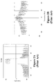
- FIGS. 2A and 2B show simulation results that illustrate the degradation in the reconstructed signal caused by a gain imbalance between two paths in a LINC amplifier.
- the vertical axis is in decibels and the horizontal axis is in megahertz.
- the input signal represents a signal that is transmitted in a bandwidth of approximately 20 MHz that is centered in the figure.
- the wings of the signal represent noise outside of the transmission bandwidth.
- the noise level of the simulated input signal is approximately 80 dB below the signal in the transmission bandwidth, as shown in FIG. 2A .
- the simulation assumes a gain imbalance of 0.1 dB between the two paths of the LINC amplifier.
- the reconstructed signal shown in FIG. 2B has a noise floor that is only approximately 10 to 30 dB below the signal in the transmission bandwidth.
- the relatively small gain imbalance of 0.1 dB significantly degrades the quality of the reconstructed amplified signal.
- the disclosed subject matter is directed to addressing the effects of one or more of the problems set forth above.
- the following presents a simplified summary of the disclosed subject matter in order to provide a basic understanding of some aspects of the disclosed subject matter. This summary is not an exhaustive overview of the disclosed subject matter. It is not intended to identify key or critical elements of the disclosed subject matter or to delineate the scope of the disclosed subject matter. Its sole purpose is to present some concepts in a simplified form as a prelude to the more detailed description that is discussed later.
- a LINC amplifier may include a signal separator for decomposing an input signal into constant envelope signals and amplifier circuits for amplifying the constant envelope signals.
- the amplifier may also include a combiner for combining the amplified constant envelope signals to form an output signal that is an amplified representation of the input signal.
- Linear correction circuits can be used to apply gain, phase, and/or delay correction to the constant envelope signals. The corrections are determined based upon a feedback portion of the output signal.
- Pre-distortion circuits can be used to apply a non-linear pre-distortion to the constant envelope signals. The non-linear pre-distortion is determined based upon the feedback portion of the output signal.
- FIG. 1 conceptually illustrates a conventional LINC amplifier with a Chireix combiner
- FIGS. 2A and 2B show simulation results that illustrate the degradation in the reconstructed signal caused by a gain imbalance between two paths in a LINC amplifier
- FIG. 3 conceptually illustrates one exemplary embodiment of a LINC amplifier
- FIG. 4 conceptually illustrates one exemplary embodiment of a decomposition of the input bounded amplitude modulated signal into two constant envelope phase modulated signals
- FIG. 5 conceptually illustrates one exemplary embodiment of a LINC separator that digitally implements calibration and compensation using analog feedback
- FIGS. 6 and 7 show simulation results that illustrate the dependence of the error vector magnitude (EVM) on phase and gain differences in the two paths of a LINC amplifier
- FIG. 8 conceptually illustrates one exemplary embodiment of a pre-distortion block
- FIG. 9 shows results of simulation of noise in the output signal for an amplifier such as the LINC amplifier shown in FIG. 3 .
- FIG. 3 conceptually illustrates one exemplary embodiment of a LINC amplifier 300 .
- the LINC amplifier 300 includes a LINC separator 305 that receives an input signal, a(t), which is a bounded amplitude and phase modulated signal.
- the separator 305 is configured to divide the input signal into two or more constant envelope phase modulated signals, u 1-n (t), which can be added to re-create the bounded amplitude-modulated input signal.
- FIG. 4 conceptually illustrates one exemplary embodiment of a decomposition of the input bounded amplitude modulated signal, a(t), into two constant envelope phase modulated signals, u 1-2 (t).
- the modulated signal is represented as
- a ⁇ ( t ) ⁇ cos ⁇ ( ⁇ ⁇ ⁇ t + ⁇ ) ( A m ⁇ ⁇ ax ⁇ 2 ) ⁇ cos ⁇ ( ⁇ ⁇ ⁇ t + ⁇ + ⁇ ) + ( A ma ⁇ ⁇ x 2 ) ⁇ cos ⁇ ( ⁇ ⁇ ⁇ t + ⁇ - ⁇ )
- the angle and maximum amplitude are defined as
- e j( ⁇ ) from e j ⁇ by rotating by the negative angle ⁇ .
- the following relations can be used to represent the above complex exponential by its coordinates:
- different implementations can be used to form the decomposed signals, including CORDIC rotations and/or Look Up Tables (LUTs) that are used to form the arccosine functions.
- the separator 305 digitally forms the constant envelope phase modulated signals and processes the sampled signals via digital signal processing hardware at a sample rate R s .
- the sample rate is chosen to provide adequate bandwidth in the digital domain to represent the signal sufficiently well such that the two (or more) signals, when reconstructed, represent an amplified version of the input signal a(t).
- the separator 305 can also generate control signals c 1-n (t) that can be used to set parameters such as the maximum gain, maximum power, or voltage depending on the class of amplifier used. In the illustrated embodiment, the control signals are provided to control circuitry 310 .
- the signals are converted from digital to analog in the radio via digital-to-analog (D/A) converters and then the signals are up-converted to radio frequencies (RF) by two or more radios 315 .
- one radio is deployed in the signal path of each of the decomposed signals.
- the radios 315 can be direct conversion or heterodyne type radios 315 or any other available type of radio.
- the signals at the output terminals of the radios 315 are then sent on to corresponding non-linear power amplifiers 320 , which may be any type of amplifier running in a non-linear mode of operation.
- Class E amplifiers are used because they are thought to provide the highest theoretical and practical efficiency.
- the output signals of the amplifiers 315 are combined in a combiner 325 , such as a Chiriex lossless combiner in the outphase modulation approach, and the output signal of the combiner 325 is then attached to the load.
- the output of the combiner 325 is also sampled by an RF coupler 330 , and the signal from the coupler 330 is brought to an observation receiver 335 that forms a digital representation of the signal at the output terminal of the combiner 325 .
- the observation receiver 335 supplies a calibration unit (not shown in FIG. 3 ) in the separator 305 with data that is compared to the transmitted source data. Calibration and compensation data is computed using the source signal and the sampled output signal.
- the plurality of radio paths, amplifiers 320 , and combiner 325 are integrated with several digital control loops (which may be digitally implemented in the separator 305 ) that provide calibration and compensation for the constant-envelope signals, amplify the constant-envelope signals, and recombine the constant-envelope signals.
- the calibration and/or compensation may be determined such that the transmitter output meets linearity, spurious emissions, and efficiency requirements, as will be discussed herein.
- the calibration loops can perform calibration and compensation for effects including group delay, gain, phase, flatness, non-linear phase and gain distortion, and the like.
- the calibration and compensation is applicable over wideband signals to allow for wideband signals and wider TX filters.
- FIG. 5 conceptually illustrates one exemplary embodiment of a LINC separator 500 that digitally implements calibration and compensation using analog feedback. Connections between the signal paths depicted in FIG. 5 are indicated by solid black circles. Otherwise, signal paths that cross in FIG. 5 are not interconnected.
- the separator 500 is used as part of a LINC amplifier (such as the amplifier 500 depicted in FIG. 5 ) and the analog feedback is provided by a radiofrequency coupler at the output of the LINC amplifier.
- the separator 500 is configured to receive a bounded-amplitude and phase-modulated input signal at input node 505 .
- the input signal, a(t) can then be provided to other elements in the separator 500 including a phase estimator 510 that is configured to determine the phase of the input signal, a signal magnitude determination unit 515 that is configured to generate a signal that represents the amplitude of the input signal,
- the output signal of the magnitude determination unit 515 can then be provided to a decomposition element 520 , which decomposes the input signal into a plurality of signals, u 1,2 (t).
- the decomposition element 520 decomposes the input signal into a pair of signals, u 1,2 (t), which are then processed using parallel signal paths in the separator 500 .
- the decomposition element 520 may implement a 64K ⁇ 16 lookup table for generating digital representations of the I-component and Q-component of the input signal, e.g., by implementing the equations discussed herein with respect to FIG. 3 .
- two signal paths are depicted leaving from the decomposition element 520 in FIG.
- the decomposition element 520 can decompose the input signal into a number of signals that can be processed using a corresponding number of parallel signal paths.
- the output of the magnitude determination unit 515 is also provided to a maximum magnitude determination unit 525 .
- the maximum magnitude determination unit 525 determines the maximum magnitude of the input signal and/or an EER maximum voltage associated with the input signal.
- the maximum magnitude determination unit 525 (and other elements in the separator 500 ) may also be controlled by a manual register overwrite. In the interest of clarity, the various manual register overwrites are not shown in FIG. 5 .
- an output signal from the maximum magnitude determination unit 525 is provided to the multiplier units 527 , 528 .
- the phase detection element 510 also provides the phase of the input signal to the multiplier units 527 , 528 .
- the maximum magnitude and a phase of the input signal can then be used to generate a pair of constant envelope signals from the I-component and Q-component of the input signal, a(t).
- Propagation along the parallel signal paths, processing by the elements on the signal paths, filtering and/or conversion of the digital signal to an analog signal, amplification, and other effects can lead to gain, phase, and/or delay imbalances between the constant envelope signals. Compensation, calibration, and pre-distortion may therefore be applied to the different branches of the signal path in the separator 500 .
- the amount of compensation, calibration, and/or pre-distortion is determined based upon feedback received from the output signal of the transmitter. Ideally, the output signal of the transmitter is an exact amplified copy of the input signal.
- a comparison of the fed back portion of the output signal and an appropriately delayed portion of the input signal can therefore be used to estimate and compute the appropriate compensation, calibration, and/or pre-distortion based on a measure of the difference between the input and output signals.
- the difference measurement is provided by an error vector magnitude, which is a waveform quality metric that measures the difference between the output signal of the combiner and the input signal.
- FIG. 6 shows simulation results that illustrate the dependence of the error vector magnitude (EVM) on phase and gain differences in the two paths of a LINC amplifier.
- the vertical axis is the error vector magnitude measured as a percentage and the horizontal axis is the gain imbalance in decibels between the two paths of the amplifier. Each curve represents a different phase imbalance between the two paths of the amplifier.
- FIG. 7 shows simulation results that also illustrate the dependence of the error vector magnitude (EVM) on phase and gain differences in the two paths of a LINC amplifier. In FIG. 7 , however, the vertical axis is the error vector magnitude measured as a percentage and the horizontal axis is the phase imbalance in degrees between the two paths of the amplifier. Each curve represents a different gain imbalance between the two paths of the amplifier.
- the error vector magnitude has a minimum value at zero gain imbalance and zero phase imbalance between the two paths of the amplifier. In some embodiments, this minimum value is a global minimum for the system.
- a portion of the input signal provided at the node 505 is delayed by the delay 517 and then provided to a gain/phase/delay engine 530 that calculates calibrations and/or compensations to the gain, phase, and/or delay of the signals.
- the amount of delay provided by the delay 517 is determined so that the calibrations and/or compensations provided by the engine 530 is applied to the portion of the signal that was used to generate the calibrations and/or compensations.
- the delay 517 is determined based upon delays that may occur in the magnitude element 515 , the decomposition element 520 , the maximum magnitude determination unit 525 , the phase determination element 510 , the multipliers 527 , 528 , and/or any other elements in the signal paths that may not be shown in FIG. 5 .
- the output signal of the combiner 325 is provided to the engine 530 as feedback via an observation receiver 532 .
- the observation receiver 532 includes a radio down conversion filter such as an analog-to-digital converter 534 and a decimation filter 535 , which are used to convert the analog feedback signal into a digital format.
- the A/D converter 534 may create the digital signal by sampling an analog signal at a rate R S .
- the sampled signal may then be provided to the decimation filter 535 , which may reduce the sampling rate of the sampled signal by a factor of N 2 so that the output signal of the observation receiver 532 has a sampling rate of R S /N 2 , which is equal to the digital sampling rate of the input signal a(t).
- the gain/phase/delay engine 530 provides linear gain, phase, and delay compensation to account for differences in line length, cabling, insertion loss/gain of the amplifier network, the combiner 325 , and the like.
- the gain/phase and delay engine 530 implements a control algorithm that minimizes a waveform quality metric, such as the Error Vector Magnitude (EVM), between the digital representation of the output signal of the combiner provided by the observation receiver 532 and the (delayed) digital input signal received at the node 505 .
- EVM Error Vector Magnitude
- Any of a variety of minimization algorithms can be used to compute the EVM and the minimization of EVM can be accomplished by varying gain/phase and delay via a gradient adaptive algorithm such as least mean square (LMS) or least squares.
- LMS least mean square
- the EVM is a sensitive measure of gain and/or phase imbalances in the system and is therefore an effective variable for controlling the gain/phase/delay engine 530 .
- the EVM has a global minimum at zero gain imbalance and zero phase imbalance so that local minima at other offsets do not interfere with operation of the control algorithm.
- the engine 530 computes the necessary linear compensation and provides this information to digital compensation filters 543 and 544 .
- the filters 543 and 544 are multiple tap digital finite impulse response filters (FIR filters).
- the digital finite impulse response filters 543 and 544 use the filter coefficients computed by engine 530 .
- each filter 543 , 544 may be comprised of multiple complex coefficients that each represents a filter tap.
- the preferred number of taps in the filters 543 , 544 may be dependent on the flatness of the system, but the actual number of taps implemented in a specific embodiment is a matter of design choice.
- the compensation filters 543 , 544 can be configured so that they have unequal gains.
- the output signals, û 1,2 (t), of the compensation filters 543 , 544 are substantially gain, phase and time aligned compensated signals and thus the signals, û 1,2 (t), are substantially aligned.
- the pre-distortion engine 545 is a phase pre-distortion engine 545 .
- the pre-distortion engine 545 may apply signal pre-distortion, path pre-distortion, gain/phase pre-distortion, and the like. The amount of delay provided by the delay 518 is determined so that the phase pre-distortion provided by the engine 545 is applied to the appropriate portion of the signal.
- the delay 518 is determined based upon delays that may occur in the magnitude element 515 , the decomposition element 520 , the maximum magnitude determination unit 525 , the phase determination element 510 , the multiplier is 527 , 528 , and/or any other elements in the signal paths that may not be shown in FIG. 5 .
- the non-linear pre-distortion applied to the signal is a function of the amplitude envelope of the input signal a(t) and so a signal that indicates the maximum value of the amplitude is generated by the maximum magnitude determination unit 525 and provided to the pre-distortion engine 545 . Feedback from a combiner (such as the combiner 325 ) is also provided to the pre-distortion engine 545 via the observation receiver 532 , as discussed herein.
- the pre-distortion engine 545 provides control signals to pre-distortion blocks 550 that apply the pre-distortion determined by the pre-distortion engine 545 .
- the control signals may be representative of the phase angles discussed above, values of coefficients of the functions that describe the mathematical function required for compensation, values of entries in a look-up table that describe the mathematical function required for compensation, and the like.
- the control signal may represent coefficients ( ⁇ kq ) to the functions that describe the phase angles.
- the pre-distortion blocks 550 also receive signals representative of the magnitude of the input signal
- Each path in the TX chain has a pre-distortion block 550 present to modulate the phase of each path as a function of the final envelope, i.e., the blocks 550 provide nonlinear phase pre-distortions that are applied using the various signals provided to the blocks 550 .
- the blocks 550 correct the effects of non-linear phase leading/lagging introduced by the combiner and/or any other elements in the system.
- the phase compensation can be used to correct phase impairments introduced by final filtering. Filtering, or sampling at rate R 1 , reduces the available bandwidth, thereby impressing a small degree of amplitude modulation on the desired constant envelope signals.
- the amplitude modulation appears as a phase modulation at the amplifier device because the device turn-on time shifts as a function of the amplitude.
- This shift in the turn-on time appears as a phase modulation that can be substantially compensated by the pre-distortion engine 545 and the pre-distortion blocks 550 , which can be configured to account for the effects of the combiner, the bandwidth limitations, and the composite phase impairments as a function of envelope.
- Spurious emissions and EVM at the output of the combiner can be used to determine the correction function coefficients in the pre-distortion engine 545 .
- the pre-distortion applied to the gain/phase/delay-corrected signals on each path can be calculated by minimizing the EVM that is computed using the path signals and the feedback provided via the observation receiver 532 .
- persons of ordinary skill in the art having benefit of the present disclosure should appreciate that other techniques for determining the pre-distortion based upon the path signals and the feedback signal may also be used.
- the signals on each path can be filtered using filters 555 to provide a digital signal to the digital-to-analog (D/A) converters 560 .
- the digital signals provided by the pre-distortion blocks 550 have a sampling rate of R.
- the filters 555 may then use interpolation to increase the sampling rate by a factor of N 1 so that the rate of the signal provided to the D/A converters 560 is R ⁇ N 1 .
- Final filtering by the filters 555 limits the bandwidth of the signal present at the amplifier device (not shown in FIG. 5 ). If the amplifier is a switched class amplifier that expects a constant envelope signal, filtering by the filters 555 can introduce amplitude modulation.
- the trade off between filtering, bandwidth, and phase pre-distortion complexity may be adjusted to minimize bandwidth, while maintaining the required EVM and spurious emissions.
- the D/A converters 560 then provide an analog representation of the signal to the radios (and the combiner) for transmission over the air interface.
- FIG. 8 conceptually illustrates one exemplary embodiment of a phase pre-distortion engine 800 , such as the phase pre-distortion engine 545 shown in FIG. 5 .
- the non-linear phase pre-distortion engine 800 provides digital phase (and gain if required) compensation to two constant envelope signals.
- the pre-distortion function provides compensation for non-linearities that occur in the transmission path, including the amplifiers and combiners. Reactive combiners can contribute significant non-linear phase distortion to the combined sum of the two constant envelope signals.
- the general form of the pre-distortion function is given by
- q indicates the number of memory terms
- k is an order of basis function ⁇ k
- ⁇ kq are coefficients of the functions k at time delay q
- n is the data sample index
- û 1,2 are the signals present at the input of the pre-distortion engine 800 .
- the magnitude of the envelope a[n] is used as the input argument (or index in a digital implementation) to the compensation function. This implies that the correction function is compensating envelope induced path non-linearity.
- ) may be any of the various functions that have been commonly used for non-linear system identification and digital pre-distortion. Common functions include:
- ⁇ ⁇ ⁇ k ⁇ ( x ) ⁇ x ⁇ k - 1 .
- Hermite polynomials, piecewise Hermite, or other functions including Forsythe synthesized orthogonal functions may also be used in this manner.
- certain functional sets may provide better correlation matrix performance, and a better fit to the system non-linearity.
- the pre-distortion engine 545 computes the coefficients, ⁇ kq , and the pre-distortion function 800 uses the coefficients (or Look Up Tables derived from the coefficients) to apply the required non-linear compensation.
- the coefficients ⁇ kq and set of functions ( ⁇ k , ⁇ k ) describe the overall function used to compensate for the non-linearity introduced by the amplifiers and combiner.
- the embodiment shown in FIG. 8 uses Look Up Tables (LUT) as a method of applying the pre-distortion function to the signals. Other embodiments may apply coefficients directly to the path or alternatively may apply a combination of coefficients and LUTs.
- LUT Look Up Tables
- FIG. 9 shows results of the simulation of noise in the output signal for an amplifier such as the LINC amplifier 300 shown in FIG. 3 .
- the vertical axis indicates the signal and/or noise level in decibels and the horizontal axis indicates frequency in megahertz.
- the signal is centered at approximately 1.96 GHz and has a 10 MHz bandwidth.
- the entire span of the horizontal axis is approximately 100 MHz.
- the upper curve 900 in FIG. 9 shows the output signal for a LINC amplifier when no calibration or compensation is provided.
- the middle curve 902 in FIG. 9 shows the output signal for the LINC amplifier following simple manual gain and phase calibration.
- the lower curve 904 in FIG. 9 shows the output signal for the LINC amplifier after applying the digital calibration, compensation, and pre-distortion techniques described herein.
- the digital techniques described herein result in a significantly better suppression of out-of-band noise.
- the out-of-band noise is suppressed by 50 or more decibels (relative to the uncorrected output signal) by the digital techniques described herein.
- Embodiments of the digital calibration, compensation, and filtering techniques described herein may have a number of advantages over the conventional practice.
- the efficiency can be dramatically increased for the least efficient component of a wireless transmitter, namely the amplification of the RF path.
- Increasing the RF path amplification efficiency decreases overall power consumption at several levels, including the transmitter, and ancillary service equipment such as battery backup, air conditioning, power conditioning.
- the operator of the higher efficiency transmitter benefits from a reduction in operational expense (OPEX), increased capacity and density, and improved reliability.
- OPEX operational expense
- CAPEX operator's capital expenditures
- the software implemented aspects of the disclosed subject matter are typically encoded on some form of program storage medium or implemented over some type of transmission medium.
- the program storage medium may be magnetic (e.g., a floppy disk or a hard drive) or optical (e.g., a compact disk read only memory, or “CD ROM”), and may be read only or random access.
- the transmission medium may be twisted wire pairs, coaxial cable, optical fiber, or some other suitable transmission medium known to the art. The disclosed subject matter is not limited by these aspects of any given implementation.
Abstract
Description
The angle and maximum amplitude are defined as
Using the unit circle shown in
u=u 1 +u 2 =x+jy=re jα =e j(α+β) +e j(α−β).
The digital signal separation function will compute two complex exponentials: u1(t)=ej(α+β) and u2 (t)=ej(α−β). The definition cos β=r/2 is used to find angle β and then ejα is transformed d into ej(α+β) by rotating a positive angle β. Similarly, we get ej(α−β) from ejα by rotating by the negative angle β. The following relations can be used to represent the above complex exponential by its coordinates:
In various embodiments, different implementations can be used to form the decomposed signals, including CORDIC rotations and/or Look Up Tables (LUTs) that are used to form the arccosine functions.
where q indicates the number of memory terms, k is an order of basis function φk, αkq are coefficients of the functions k at time delay q, and n is the data sample index, û1,2 are the signals present at the input of the
-
- Conventional polynomials:
-
- Shifted Legendre polynomials:
Alternatively, Hermite polynomials, piecewise Hermite, or other functions including Forsythe synthesized orthogonal functions may also be used in this manner. Depending on the nature of the non-linearity, certain functional sets may provide better correlation matrix performance, and a better fit to the system non-linearity. The
Claims (12)
Priority Applications (6)
| Application Number | Priority Date | Filing Date | Title |
|---|---|---|---|
| US12/487,206 US8026762B2 (en) | 2009-06-18 | 2009-06-18 | High efficiency transmitter for wireless communication |
| JP2012516105A JP5432374B2 (en) | 2009-06-18 | 2010-06-01 | High efficiency transmitter for wireless communication |
| EP10730890.0A EP2443739B1 (en) | 2009-06-18 | 2010-06-01 | A high efficiency transmitter for wireless communication |
| CN201080027125.3A CN102460956B (en) | 2009-06-18 | 2010-06-01 | A high efficiency transmitter for wireless communication |
| KR1020117030017A KR101286483B1 (en) | 2009-06-18 | 2010-06-01 | An amplifier and a method for amplifying a signal |
| PCT/US2010/036801 WO2010147754A1 (en) | 2009-06-18 | 2010-06-01 | A high efficiency transmitter for wireless communication |
Applications Claiming Priority (1)
| Application Number | Priority Date | Filing Date | Title |
|---|---|---|---|
| US12/487,206 US8026762B2 (en) | 2009-06-18 | 2009-06-18 | High efficiency transmitter for wireless communication |
Publications (2)
| Publication Number | Publication Date |
|---|---|
| US20100321107A1 US20100321107A1 (en) | 2010-12-23 |
| US8026762B2 true US8026762B2 (en) | 2011-09-27 |
Family
ID=42670579
Family Applications (1)
| Application Number | Title | Priority Date | Filing Date |
|---|---|---|---|
| US12/487,206 Expired - Fee Related US8026762B2 (en) | 2009-06-18 | 2009-06-18 | High efficiency transmitter for wireless communication |
Country Status (6)
| Country | Link |
|---|---|
| US (1) | US8026762B2 (en) |
| EP (1) | EP2443739B1 (en) |
| JP (1) | JP5432374B2 (en) |
| KR (1) | KR101286483B1 (en) |
| CN (1) | CN102460956B (en) |
| WO (1) | WO2010147754A1 (en) |
Cited By (2)
| Publication number | Priority date | Publication date | Assignee | Title |
|---|---|---|---|---|
| US20120314746A1 (en) * | 2011-06-08 | 2012-12-13 | Broadcom Corporation | Controlling a Transmit Path Based on Monitored Error Vector Magnitude (EVM) Performance |
| US20210341567A1 (en) * | 2020-05-04 | 2021-11-04 | Nxp B.V. | Predistortion technique for joint radar/communication systems |
Families Citing this family (25)
| Publication number | Priority date | Publication date | Assignee | Title |
|---|---|---|---|---|
| TWI536661B (en) * | 2009-04-13 | 2016-06-01 | 凡爾賽特公司 | System for communication and method for communicating rf signals |
| US10516219B2 (en) | 2009-04-13 | 2019-12-24 | Viasat, Inc. | Multi-beam active phased array architecture with independent polarization control |
| US8693970B2 (en) | 2009-04-13 | 2014-04-08 | Viasat, Inc. | Multi-beam active phased array architecture with independant polarization control |
| US8030998B2 (en) * | 2009-04-13 | 2011-10-04 | Viasat, Inc. | Active feed forward amplifier |
| EP2419962B1 (en) * | 2009-04-13 | 2020-12-23 | ViaSat, Inc. | Half-duplex phased array antenna system |
| US8787768B2 (en) * | 2010-06-03 | 2014-07-22 | Raytheon Company | Method and apparatus for synthesizing and correcting phase distortions in ultra-wide bandwidth optical waveforms |
| JP5633367B2 (en) * | 2010-12-28 | 2014-12-03 | 富士通株式会社 | Amplification apparatus and amplification method |
| JP5605271B2 (en) * | 2011-03-01 | 2014-10-15 | 富士通株式会社 | Synthetic amplifier, transmitter, and synthetic amplifier control method |
| US8891675B2 (en) * | 2011-10-04 | 2014-11-18 | Texas Instruments Incorporated | Power-indexed look-up table design of digital pre-distortion for power amplifiers with dynamic nonlinearities |
| US8737531B2 (en) * | 2011-11-29 | 2014-05-27 | Viasat, Inc. | Vector generator using octant symmetry |
| US8699626B2 (en) * | 2011-11-29 | 2014-04-15 | Viasat, Inc. | General purpose hybrid |
| JP2013115725A (en) * | 2011-11-30 | 2013-06-10 | Asahi Kasei Electronics Co Ltd | Distortion compensator |
| JP5867304B2 (en) | 2012-06-19 | 2016-02-24 | 富士通株式会社 | Amplification apparatus and amplification method |
| JP5906967B2 (en) * | 2012-06-29 | 2016-04-20 | 富士通株式会社 | Distortion compensation apparatus and distortion compensation method |
| US9595920B2 (en) * | 2013-03-22 | 2017-03-14 | Massachusette Institute Of Technology | Hardware-efficient compensator for outphasing power amplifiers |
| US9025699B2 (en) * | 2013-05-13 | 2015-05-05 | Samsung Electronics Co., Ltd. | Methods and apparatus for all digital multi-level outphasing using bandwidth reduction |
| WO2014202112A1 (en) * | 2013-06-17 | 2014-12-24 | Nokia Solutions And Networks Oy | A radio transmitter with amplifier paths having out-phased radio frequency signals |
| US20160034421A1 (en) * | 2014-08-01 | 2016-02-04 | Infineon Technologies Ag | Digital pre-distortion and post-distortion based on segmentwise piecewise polynomial approximation |
| JP2016127577A (en) | 2015-01-08 | 2016-07-11 | 富士通株式会社 | Distortion compensation device and distortion compensation method |
| CN106446323B (en) * | 2016-07-20 | 2019-07-09 | 成都能通科技有限公司 | Time delay antidote based on amplitude difference variance minimum decision rule |
| US9935810B1 (en) * | 2017-03-07 | 2018-04-03 | Xilinx, Inc. | Method and apparatus for model identification and predistortion |
| JP6769544B2 (en) * | 2017-03-21 | 2020-10-14 | 日本電気株式会社 | Amplification device and amplification method |
| WO2018219466A1 (en) * | 2017-06-01 | 2018-12-06 | Telefonaktiebolaget Lm Ericsson (Publ) | Digital predistortion for advanced antenna system |
| JP7206719B2 (en) * | 2017-10-31 | 2023-01-18 | 富士通株式会社 | Distortion compensation device and distortion compensation method |
| CA3119673A1 (en) | 2018-11-13 | 2020-05-22 | Telefonaktiebolaget Lm Ericsson (Publ) | Active antenna array linearization |
Citations (6)
| Publication number | Priority date | Publication date | Assignee | Title |
|---|---|---|---|---|
| US6054896A (en) * | 1998-12-17 | 2000-04-25 | Datum Telegraphic Inc. | Controller and associated methods for a linc linear power amplifier |
| US6633200B2 (en) * | 2000-06-22 | 2003-10-14 | Celiant Corporation | Management of internal signal levels and control of the net gain for a LINC amplifier |
| US20060153147A1 (en) | 2000-12-28 | 2006-07-13 | Gopal Chillariga | Fast macrodiversity switching with timing management in wireless networks |
| US20070280175A1 (en) | 2006-06-01 | 2007-12-06 | Fang-Chen Cheng | Coordinating transmission scheduling among multiple base stations |
| US20100105338A1 (en) * | 2008-10-29 | 2010-04-29 | Yongtao Wang | Predistortion methods and apparatus for transmitter linearization in a communication transceiver |
| US7737778B2 (en) * | 2003-07-03 | 2010-06-15 | Aryan Saed | Adaptive predistortion for a transmit system |
Family Cites Families (5)
| Publication number | Priority date | Publication date | Assignee | Title |
|---|---|---|---|---|
| CA2281209A1 (en) * | 1998-10-30 | 2000-04-30 | Norman Gerard Ziesse | Feedforward amplifier and method of amplifying signals |
| JP2006060451A (en) * | 2004-08-19 | 2006-03-02 | Matsushita Electric Ind Co Ltd | Power amplifier and delay measuring method for power combining system |
| US8031804B2 (en) * | 2006-04-24 | 2011-10-04 | Parkervision, Inc. | Systems and methods of RF tower transmission, modulation, and amplification, including embodiments for compensating for waveform distortion |
| WO2008044268A1 (en) * | 2006-10-05 | 2008-04-17 | Panasonic Corporation | Transmitter apparatus and transmitting method |
| WO2008117399A1 (en) * | 2007-03-26 | 2008-10-02 | Panasonic Corporation | Amplifier circuit |
-
2009
- 2009-06-18 US US12/487,206 patent/US8026762B2/en not_active Expired - Fee Related
-
2010
- 2010-06-01 WO PCT/US2010/036801 patent/WO2010147754A1/en active Application Filing
- 2010-06-01 JP JP2012516105A patent/JP5432374B2/en not_active Expired - Fee Related
- 2010-06-01 KR KR1020117030017A patent/KR101286483B1/en active IP Right Grant
- 2010-06-01 CN CN201080027125.3A patent/CN102460956B/en not_active Expired - Fee Related
- 2010-06-01 EP EP10730890.0A patent/EP2443739B1/en not_active Not-in-force
Patent Citations (6)
| Publication number | Priority date | Publication date | Assignee | Title |
|---|---|---|---|---|
| US6054896A (en) * | 1998-12-17 | 2000-04-25 | Datum Telegraphic Inc. | Controller and associated methods for a linc linear power amplifier |
| US6633200B2 (en) * | 2000-06-22 | 2003-10-14 | Celiant Corporation | Management of internal signal levels and control of the net gain for a LINC amplifier |
| US20060153147A1 (en) | 2000-12-28 | 2006-07-13 | Gopal Chillariga | Fast macrodiversity switching with timing management in wireless networks |
| US7737778B2 (en) * | 2003-07-03 | 2010-06-15 | Aryan Saed | Adaptive predistortion for a transmit system |
| US20070280175A1 (en) | 2006-06-01 | 2007-12-06 | Fang-Chen Cheng | Coordinating transmission scheduling among multiple base stations |
| US20100105338A1 (en) * | 2008-10-29 | 2010-04-29 | Yongtao Wang | Predistortion methods and apparatus for transmitter linearization in a communication transceiver |
Non-Patent Citations (2)
| Title |
|---|
| International Search Report PCT/US2010/036801 dated Sep. 17, 2010. |
| Written Opinion dated Dec. 17, 2010. |
Cited By (4)
| Publication number | Priority date | Publication date | Assignee | Title |
|---|---|---|---|---|
| US20120314746A1 (en) * | 2011-06-08 | 2012-12-13 | Broadcom Corporation | Controlling a Transmit Path Based on Monitored Error Vector Magnitude (EVM) Performance |
| US8837635B2 (en) * | 2011-06-08 | 2014-09-16 | Broadcom Corporation | Controlling a transmit path based on monitored error vector magnitude (EVM) performance |
| US20210341567A1 (en) * | 2020-05-04 | 2021-11-04 | Nxp B.V. | Predistortion technique for joint radar/communication systems |
| US11550027B2 (en) * | 2020-05-04 | 2023-01-10 | Nxp B.V. | Predistortion technique for joint radar/communication systems |
Also Published As
| Publication number | Publication date |
|---|---|
| CN102460956A (en) | 2012-05-16 |
| EP2443739A1 (en) | 2012-04-25 |
| JP2012531095A (en) | 2012-12-06 |
| JP5432374B2 (en) | 2014-03-05 |
| US20100321107A1 (en) | 2010-12-23 |
| WO2010147754A1 (en) | 2010-12-23 |
| CN102460956B (en) | 2015-04-29 |
| KR20120026549A (en) | 2012-03-19 |
| KR101286483B1 (en) | 2013-07-16 |
| EP2443739B1 (en) | 2013-05-08 |
Similar Documents
| Publication | Publication Date | Title |
|---|---|---|
| US8026762B2 (en) | High efficiency transmitter for wireless communication | |
| US8442460B2 (en) | Method for compensating signal distortions in composite amplifiers | |
| US7403573B2 (en) | Uncorrelated adaptive predistorter | |
| EP1705801B1 (en) | Distortion compensation apparatus | |
| EP1204216B1 (en) | Method and apparatus for distortion compensation of radio device | |
| US8588332B2 (en) | Dynamic digital pre-distortion system | |
| US20180227152A1 (en) | Modulation agnostic digital hybrid mode power amplifier system and method | |
| US6885241B2 (en) | Type-based baseband predistorter function estimation technique for non-linear circuits | |
| CA2679114C (en) | Linearization of rf power amplifiers using an adaptive subband predistorter | |
| US7330073B2 (en) | Arbitrary waveform predistortion table generation | |
| US8824980B2 (en) | System and method to implement a radio transmitter with digital predistortion having reduced noise | |
| US20100074367A1 (en) | Adaptive combiner error calibration algorithms in all-digital outphasing transmitter | |
| EP2858251B1 (en) | Distortion compensation device and distortion compensation method | |
| US20110065381A1 (en) | Method of transmitting higher power from a satellite by more efficiently using the existing satellite power amplifiers | |
| Huang et al. | Efficient transmitter self-calibration and amplifier linearization techniques | |
| Huang et al. | Benefit of linearizing power amplifiers in multi-port amplifier subsystems |
Legal Events
| Date | Code | Title | Description |
|---|---|---|---|
| AS | Assignment |
Owner name: ALCATEL-LUCENT U.S.A., INC., NEW JERSEY Free format text: ASSIGNMENT OF ASSIGNORS INTEREST;ASSIGNOR:HONCHARENKO, WALTER;REEL/FRAME:023329/0372 Effective date: 20091001 |
|
| FEPP | Fee payment procedure |
Free format text: PAYOR NUMBER ASSIGNED (ORIGINAL EVENT CODE: ASPN); ENTITY STATUS OF PATENT OWNER: LARGE ENTITY |
|
| ZAAA | Notice of allowance and fees due |
Free format text: ORIGINAL CODE: NOA |
|
| ZAAB | Notice of allowance mailed |
Free format text: ORIGINAL CODE: MN/=. |
|
| AS | Assignment |
Owner name: ALCATEL LUCENT, FRANCE Free format text: ASSIGNMENT OF ASSIGNORS INTEREST;ASSIGNOR:ALCATEL-LUCENT USA INC.;REEL/FRAME:026494/0767 Effective date: 20110621 |
|
| STCF | Information on status: patent grant |
Free format text: PATENTED CASE |
|
| AS | Assignment |
Owner name: CREDIT SUISSE AG, NEW YORK Free format text: SECURITY AGREEMENT;ASSIGNOR:LUCENT, ALCATEL;REEL/FRAME:029821/0001 Effective date: 20130130 Owner name: CREDIT SUISSE AG, NEW YORK Free format text: SECURITY AGREEMENT;ASSIGNOR:ALCATEL LUCENT;REEL/FRAME:029821/0001 Effective date: 20130130 |
|
| AS | Assignment |
Owner name: ALCATEL LUCENT, FRANCE Free format text: RELEASE BY SECURED PARTY;ASSIGNOR:CREDIT SUISSE AG;REEL/FRAME:033868/0001 Effective date: 20140819 |
|
| FPAY | Fee payment |
Year of fee payment: 4 |
|
| MAFP | Maintenance fee payment |
Free format text: PAYMENT OF MAINTENANCE FEE, 8TH YEAR, LARGE ENTITY (ORIGINAL EVENT CODE: M1552); ENTITY STATUS OF PATENT OWNER: LARGE ENTITY Year of fee payment: 8 |
|
| FEPP | Fee payment procedure |
Free format text: MAINTENANCE FEE REMINDER MAILED (ORIGINAL EVENT CODE: REM.); ENTITY STATUS OF PATENT OWNER: LARGE ENTITY |
|
| LAPS | Lapse for failure to pay maintenance fees |
Free format text: PATENT EXPIRED FOR FAILURE TO PAY MAINTENANCE FEES (ORIGINAL EVENT CODE: EXP.); ENTITY STATUS OF PATENT OWNER: LARGE ENTITY |
|
| STCH | Information on status: patent discontinuation |
Free format text: PATENT EXPIRED DUE TO NONPAYMENT OF MAINTENANCE FEES UNDER 37 CFR 1.362 |
|
| FP | Lapsed due to failure to pay maintenance fee |
Effective date: 20230927 |