US8059280B2 - Method for three-dimensional imaging using multi-phase structured light - Google Patents
Method for three-dimensional imaging using multi-phase structured light Download PDFInfo
- Publication number
- US8059280B2 US8059280B2 US12/023,484 US2348408A US8059280B2 US 8059280 B2 US8059280 B2 US 8059280B2 US 2348408 A US2348408 A US 2348408A US 8059280 B2 US8059280 B2 US 8059280B2
- Authority
- US
- United States
- Prior art keywords
- feature
- height
- images
- fringe
- projected
- Prior art date
- Legal status (The legal status is an assumption and is not a legal conclusion. Google has not performed a legal analysis and makes no representation as to the accuracy of the status listed.)
- Active, expires
Links
Images


Classifications
-
- G—PHYSICS
- G01—MEASURING; TESTING
- G01B—MEASURING LENGTH, THICKNESS OR SIMILAR LINEAR DIMENSIONS; MEASURING ANGLES; MEASURING AREAS; MEASURING IRREGULARITIES OF SURFACES OR CONTOURS
- G01B11/00—Measuring arrangements characterised by the use of optical techniques
- G01B11/24—Measuring arrangements characterised by the use of optical techniques for measuring contours or curvatures
- G01B11/25—Measuring arrangements characterised by the use of optical techniques for measuring contours or curvatures by projecting a pattern, e.g. one or more lines, moiré fringes on the object
- G01B11/2536—Measuring arrangements characterised by the use of optical techniques for measuring contours or curvatures by projecting a pattern, e.g. one or more lines, moiré fringes on the object using several gratings with variable grating pitch, projected on the object with the same angle of incidence
-
- G—PHYSICS
- G01—MEASURING; TESTING
- G01B—MEASURING LENGTH, THICKNESS OR SIMILAR LINEAR DIMENSIONS; MEASURING ANGLES; MEASURING AREAS; MEASURING IRREGULARITIES OF SURFACES OR CONTOURS
- G01B11/00—Measuring arrangements characterised by the use of optical techniques
- G01B11/02—Measuring arrangements characterised by the use of optical techniques for measuring length, width or thickness
- G01B11/06—Measuring arrangements characterised by the use of optical techniques for measuring length, width or thickness for measuring thickness ; e.g. of sheet material
- G01B11/0608—Height gauges
-
- G—PHYSICS
- G06—COMPUTING; CALCULATING OR COUNTING
- G06T—IMAGE DATA PROCESSING OR GENERATION, IN GENERAL
- G06T7/00—Image analysis
- G06T7/50—Depth or shape recovery
- G06T7/521—Depth or shape recovery from laser ranging, e.g. using interferometry; from the projection of structured light
Definitions
- a circuit board substrate is prepared with predetermined conductor paths and pads for receiving the lead of an electronic component such as integrated circuit chips, resistors or capacitors.
- solder paste bricks are placed onto the board substrate at appropriate positions.
- the solder paste is usually applied by placing a screen onto the substrate, applying solder paste through the screen openings and removing the screen from the substrate.
- the circuit board electronic components are then positioned onto the substrate, preferably with a pick and place machine, with the leads of the electronic components placed on the respective solder paste bricks.
- the circuit board is passed through an oven after all of the components are positioned on a substrate to melt the solder paste thus creating an electrical as well as mechanical connection between the components and the substrate.
- solder paste brick heights can be as small as 100 microns and the height of the solder paste brick must often be measured to within 1 percent of the designed height and size.
- the center-to-center spacing between solder bricks is sometimes 200 microns. Too little solder paste can result in no electrical connection between the lead of an electronic component and the pad of the circuit board substrate. Too much paste can result in bridging and short-circuiting between the leads of a component.
- a single circuit board can cost thousands or even tens of thousands of dollars to manufacture. Testing of a circuit board after the fabrication process is complete can detect errors in solder paste placement and component lead connection, but often the only remedy for a faulty board is the rejection of the entire board. It is accordingly imperative that a circuit board be inspected during the fabrication process so that improper solder paste placement can be detected prior to the placement of the electronic components onto the substrate. Such in-process solder inspection reduces the cost of failure since expensive components have not yet been placed onto the circuit board.
- Embodiments of the present invention are applicable to a variety of automated optical inspections relative to electronics manufacture. Important inspections include, solder paste inspection, adhesive or glue inspection, post-placement component inspection, lead/ball coplanarity inspection, et cetera.
- U.S. Pat. No. 6,750,899 assigned to the Assignee of the present application, provides a height topology inspection system that is able to detect the size and height of solder paste by projecting light through a reticle so as to project a pattern of light onto an area of the printed circuit board.
- a board transport positions the board to at least two different positions, where each position corresponds to a different phase of the projected light.
- An image corresponding to each respective position phase is acquired at each position.
- the relative movement between the sensor and the board is measured, and a processor co-sites the at least two images and constructs a height map image with the co-sited images.
- the height map image is then used to detect size and height of solder paste on a circuit board.
- a method for mapping height of a feature upon a test surface includes projecting patterned illumination upon the feature, the patterned illumination having a plurality of distinct fringe periods.
- a first image of the feature is acquired while the patterned illumination is projected upon the feature.
- Relative movement is then generated between a sensor and the feature to cause relative displacement of a fraction of a field of view of a detector, the fraction being equal to about an inverse of the number of distinct regions of a reticle generating the pattern.
- a second image of the feature is acquired while the patterned illumination is projected upon the feature.
- the height map is generated based, at least, upon the first and second images.
- FIG. 1 is a diagrammatic view of a height topology inspection system with which embodiments of the present invention are useful.
- FIG. 2 is a diagrammatic view of a reticle pattern of a prior-art profilometer projected upon a flat surface.
- FIG. 3 is a diagrammatic view of a multi-phase reticle pattern projected in accordance with an embodiment of the present invention.
- FIG. 4 is a flow diagram of a method of three-dimensionally imaging a test surface using multi-phase structured light in accordance with an embodiment of the present invention.
- FIG. 5 is a timing chart illustrating Y-axis sensor displacement and fringe image acquisition over time, in accordance with an embodiment of the present invention.
- FIG. 6 is a diagrammatic view of a multi-phase reticle pattern projected in accordance with another embodiment of the present invention.
- Embodiments of the present invention generally employ a technique for mapping, or otherwise measuring, height of a feature, such as solder paste, on a circuit board.
- Three-dimensional phase profilometry is a known technique. See, for example, U.S. Pat. Nos. 6,049,384 and 6,750,899, which patents issued to the assignee of the current application.
- a light pattern is projected onto a substrate and is analogous to the pattern of dark and light areas cast onto a floor by sunlight passing through a Venetian blind.
- the pattern of light on a flat surface will be one of parallel, straight stripes, but varying in intensity according to the sinusoidal pattern of opacity of the reticle.
- the pattern of stripes of sunlight will be shifted laterally if they strike an object (like a sleeping cat) having a height different from the height of the flat floor.
- the pattern of stripes presented on the flat surface is shifted laterally from the presence of an object having a height different from the height of the flat surface.
- FIG. 1 shows a height topology inspection system 10 , which includes processor 14 , X-Y motion system 16 and optical sensor system 18 .
- height topology inspection system 10 is as a solder paste inspection system, but those skilled in the art will recognize that system 10 can be used for other suitable types of topology inspections.
- Solder paste inspection system 10 is coupleable to host device 19 through network 21 or the like, in order to send and receive information related to solder inspection on printed circuit boards.
- system 10 may receive location information relating to specific solder paste locations, and their respective nominal volume.
- processor 14 is disposed within microcomputer 12 , which microcomputer 12 is a known device having an input such as a keyboard, and mouse, and an output in the form of a video monitor.
- microcomputer 12 preferably includes an industry-standard architecture and microprocessor.
- microcomputer 12 preferably includes an industry-standard architecture and microprocessor.
- microcomputer 12 is a personal computer running a Microsoft Windows® operating system with an Intel Pentium® processor.
- Processor 14 is preferably embodied upon a computer peripheral card with an industry-standard form factor. Further, processor 14 is preferably adapted to couple to microcomputer 12 through a standard Peripheral Component Interconnect (PCI) bus. Processor 14 can then transfer data to and from microcomputer 12 using a known Direct Memory Access (DMA) transfer method to facilitate high-speed data transfer.
- PCI Peripheral Component Interconnect
- DMA Direct Memory Access
- Processor 14 receives the digital video data from analog/digital electronics 48 and performs a number of functions on such data. For example, processor 14 triggers sensor system 18 to acquire images based upon encoder information received from encoders 24 through line 20 . Processor 14 also communicates with sensor system 18 in order to control its operational mode (i.e. high-resolution vs. high-speed). Processor 14 receives previously digitized video data from sensor system 18 for storage in a frame buffer (not shown). Processor 14 operates upon the digitized video images to correct for defects in the particular CMOS array 46 in sensor system 18 . Processor 14 is also used to compensate for effects of known optical distortions on the height map.
- processor 14 triggers sensor system 18 to acquire images based upon encoder information received from encoders 24 through line 20 .
- Processor 14 also communicates with sensor system 18 in order to control its operational mode (i.e. high-resolution vs. high-speed).
- Processor 14 receives previously digitized video data from sensor system 18 for storage in a
- Processor 14 is coupled to X-Y motion system 16 through line 20 .
- X-Y motion system 16 also includes X and Y motors (not shown) which position circuit board 22 in respective X and Y axes.
- X and Y motors are operably coupled to X and Y encoders (shown diagrammatically at block 24 ) to provide data indicative of circuit board position along X and Y axes to processor 14 .
- Motion commands are sent over line 25 to system 16 .
- System 16 is extraordinarily stable and its motion is controlled to within approximately a fraction of a pixel size over the distance required to acquire at least two phase images used to generate a height map. If system 16 is not sufficiently stable, additional processing in the electronics may be needed to provide equivalent accuracy and repeatability.
- each of the linear encoders preferably has a resolution of about 0.5 ⁇ m, as can be purchased from Renishaw.
- computer 12 and X-Y motion system 16 precisely move circuit board 22 as desired in the X and Y directions at arrows 7 , 8 , respectively.
- Optical sensor system 18 includes camera system 30 and projection system 28 .
- Camera system 30 includes camera lens 31 , a CMOS detector 46 and a set of A/D electronics 48 .
- Projection system 28 includes flashlamp 38 , condenser 40 , reticle 41 and projector lens 42 . All the components within system 18 are fixed within a housing for the system. System 18 is fixedly attached to a translation stage (not shown) to provide z movement for focus control.
- Flashlamp 38 is preferably a high-speed strobe lamp filled with xenon gas, projecting broadband white light.
- a high speed discharge circuit (not shown) within housing 18 drives lamp 38 , as timing signals through channel 34 cause lamp 38 to fire multiple times within a short period of time, preferably at least one millisecond between strobes in order to ensure that the flashlamp remains stable.
- High speed discharge circuits capable of providing three flashes within such a short time are critical to ensuring high system throughput.
- Condenser lens 40 collects light from flashlamp 38 and directs it through reticle 41 to the projector lens 42 , which forms sinusoidally varying fringe images on the test surface 36 .
- reticle 41 has an astigmatic pattern and the projector lens is astigmatic, together reliably forming sinusoidally varying astigmatic patterns with low harmonic distortion.
- Projector lens system 28 is preferably doubly telecentric, in that it is telecentric in reticle space and target space (at solder paste deposits 36 on board 22 ).
- the double telecentricity is important since it allows the height, volume and area calculations to be independent of the location of the solder paste within the field of view and depth of focus. This characteristic also provides lower distortion for the system as a whole, which is important because the target moves between exposures.
- Camera system 30 views the projected fringes on the target of solder paste deposits 36 , and acquires and digitizes images in rapid succession.
- Camera system 30 does not include a grating, as is incorporated in moiré interferometry systems.
- camera system 30 is telecentric in target space and has low distortion for the same reasons given above.
- the size of the field of view is selected to maximize the field coverage while still maintaining sufficient resolution of the target.
- CMOS array 46 is a preferably a megapixel array and as such is able to inspect solder paste features of fine detail. For example, solder features for components such as a Chip Scale Package (CSP) or a microball grid array can be inspected. However, by sampling or combining data from individual pixels, larger equivalent pixels are generated which facilitates inspection at higher speeds.
- CSP Chip Scale Package
- the inspection mode can be rapidly switched between the high-resolution mode and the high-speed mode for different solder paste features on the same board, based upon the type of components that will be found in different areas of board 22 .
- optical sensor system 18 employs a dual-resolution capability in the same unit.
- phase wrap produces height ambiguities due to the cyclic nature of the phase reconstruction technique. This problem is especially troubling for surfaces that have height variations that are larger than the phase period of the sensor as well as for surfaces that have discontinuous step height profiles. Attempts to address this problem generally include the addition of a second sensor or the modification of the fringe frequency within the image source generator. Adding a second sensor is a more expensive approach since two separate optical paths are required. Additionally, adding a method to change the fringe frequency with the same image source generator adds cost to the profilometer and requires multiple read cycles from the receive camera thereby slowing down the data acquisition rate of the sensor.
- Embodiments of the present invention generally overcome deficiencies of previous attempts and provide a three-dimensional imaging system that has a vastly expanded effective height envelope without extra costs and speed penalties.
- FIG. 2 is a diagrammatic view of a reticle pattern of a prior-art profilometer projected upon a flat surface.
- pattern 100 is composed of a plurality of parallel lines of varying darkness arranged, preferably at an angle such as 45°, with respect to the direction of relative motion between the profilometer and the workpiece.
- the distance between the cycles of the pattern in FIG. 2 is considered the fringe period.
- FIG. 3 is a diagrammatic view of a multi-phase reticle pattern projected in accordance with an embodiment of the present invention.
- reticle pattern 200 bears some similarities to reticle pattern 100 in that it is comprised of a number of parallel lines that are generally at an angle with respect to the direction of relative motion between the sensor and the circuit board.
- reticle pattern 200 includes a plurality of distinct phase regions. Specifically, region 202 has a relatively short fringe period thereby allowing very high precision, but also having a relatively low wrap height.
- Region 204 is disposed adjacent region 202 and has a fringe period that is different, in this case greater, than the fringe period of region 202 . As illustrated in FIG.
- the different regions 202 , 204 are preferably aligned with each other. Further, the size of each fringe region 202 , 204 is preferably equal. This preference remains even when additional fringe regions having still other fringe periods are employed. For example, if three regions are used, it is convenient that each of the three regions be of the same size.
- one fringe period may be relatively large, for coarse height mapping. As long as the coarse height mapping function can determine a height to within the wrapping height of the second fringe period, it will be useful.
- a first fringe period may be very precise, but have a wrap height of only 1 millimeter.
- a second fringe period may have a wrap height of 9 millimeters, but be able to discern height to within 1 millimeter.
- the precision of the smaller fringe period can be used to obtain very precise height mapping within the entire height envelope of the larger fringe period.
- Other combinations of distinct fringe periods are also contemplated.
- fringe periods only one of the fringe periods provides the extremely fine height precision, and the other is used for coarse height determination.
- two relatively similar fringe periods can be used to potentially provide an unambiguous, precision height map over a distance greater than the wrap height of each individual fringe height map.
- a fringe period having a wrap height of 1 millimeter used with a second fringe period having a wrap height of 1.2 millimeters will allow each to contribute to the precise height mapping and will provide a wrap height of 6 millimeters. This is because within the 6 millimeter height, the height information derived from the combination of each fringe period will only resolve to a single height within the 6 millimeter height envelope.
- FIG. 4 is a flow diagram of a method of three-dimensionally imaging a test surface using multi-phase structured light in accordance with an embodiment of the present invention.
- sensor 18 is moved relative to the test surface 22 in the Y axis 8 as indicated in FIG. 1 .
- Method 300 begins at block 302 , where control passes to block 304 .
- the height scanning apparatus in initialized. Such initialization can include zeroing any suitable variables and/or registers, as well as starting the motion profile.
- control passes to block 306 where the sensor is moved to a “next” location. This location is the location of a feature on the surface to be tested.
- block 308 begins, which is the overall height image acquisition process.
- block 310 executes first by acquiring a first image (Image A).
- Block 310 includes substeps 310 A, 310 B and 310 C.
- the fringe illuminator is triggered.
- illumination preferably strobed illumination
- the illuminator is preferably triggered by stage encoders 24 when the sensor is positioned to acquire the first fringe image.
- fringe image 1 A is accessed and stored.
- fringe image 2 A is accessed and stored.
- the illuminator projects the image of the reticle onto the test surface and an image is acquired on the area array imager. The image is downloaded from the imager and stored in memory of the controller. Accordingly, Fringe images 1 A and 2 A are acquired at the same time since they are within the same field of view of CMOS detector 46 .
- Image B is acquired. Like block 310 , block 314 includes substeps 314 A, 314 B, and 314 C.
- the fringe illuminator is triggered.
- illumination preferably strobed illumination
- fringe image 1 B is accessed and stored.
- fringe image 2 B is accessed and stored. Fringe images 1 B and 2 B are acquired at the same time since they are within the same field of view of CMOS detector 46 .
- Block 318 Image C is acquired. Like blocks 310 and 314 , block 318 includes substeps 318 A, 318 B, and 318 C.
- the fringe illuminator is triggered.
- illumination preferably strobed, is fired through a reticle, such as reticle 41 , that has two distinct fringe patterns. This generates two distinct patterns within the field of view of CMOS sensor 46 .
- fringe image 1 C is accessed and stored.
- fringe image 2 C is accessed and stored. Fringe images 1 C and 2 C are acquired at the same time since they are within the same field of view of CMOS detector 46 .
- the Nth Height Image is computed for Fringes 1 and 2 , respectively.
- the Nth height image computed for Fringe 1 is combined with the (N ⁇ 1)th height image for Fringe Image 2 to produce an extended range height image.
- Control then passes to block 326 where the system determines if the scan is complete. If the scan is complete, control passes to block 328 where the method ends. However, if the scan is not complete, control returns to block 306 via line 330 and the system moves to the “next” (N+1) location. Further, the movement between the current location (N) and the “next” location is preferably a fraction of the field of view of the CMOS detector. In embodiments where more than two distinct fringe periods are employed, the fraction is preferably equal to about an inverse of the number of distinct regions of the reticle generating the pattern.
- the two, or more, fringe period areas can be acquired by the area array imager and processed separately as two distinct height maps.
- the two or more height images generated by the two or more areas of the fringe image represent different areas of the test surface.
- the sensor is required to move relative to the test surface and if the image areas of differing fringe period are aligned along the axis of sensor motion, each of the areas defined by the two fringe periods will be able to acquire an image of the test surface.
- the individual height images can be compared and combined to extend the height range of the measurement past the wrap height of a single fringe image.
- FIG. 5 is a time chart illustrating Y-axis sensor displacement and fringe image acquisition over time, in accordance with an embodiment of the present invention.
- a reticle image having fringe patterns 1 and 2 is projected at position y 0 . While this reticle image is projected (fringes 1 and 2 ) two, or preferably three, varying phase images are acquired. As is shown in U.S. Pat. No. 6,750,899, these images have a phase difference (such as three images being acquired at a phase difference of 120 degrees) that allows the a height map relative to the first time frame to be constructed. As can be seen in FIG.
- the image acquisitions during time frame t 0 do not last until time frame t 1 , instead there is a time lag between t 0 and t 1 , where the sensor moves in the Y-axis to the next position.
- This delay is described with respect to block 306 in FIG. 4 .
- the sensor moves such that the images acquired during time frame t 1 include a portion of overlap in sensor field of view with the images acquired during time frame t 0 .
- fringe pattern 1 in time frame t 1 overlaps with fringe pattern 2 from time frame t 0 .
- this process continues until the sensor has scanned, or otherwise sensed, the entire Y-axis.
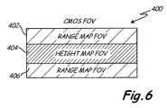
- FIG. 6 is a diagrammatic view of a multi-phase reticle pattern projected in accordance with another embodiment of the present invention.
- Pattern 400 includes three distinct regions. Specifically, pattern 400 includes regions 402 , 404 , and 406 . As can be seen in FIG. 6 , region 404 is a height map region having a relatively smaller fringe period than regions 402 , 406 . Accordingly, when region 404 is projected upon a test surface, fine height detail can be ascertained. However, since the workpiece may not lay truly flat, one of regions 402 , 404 can be used to coarsely determine height prior to the acquisition of an image bearing region 404 . This allows the sensor Z height to be adjusted in order to provide better focus for the height map image.
- an image of region 404 upon the test surface is acquired. This allows the system to dynamically change focus to follow a board or workpiece that does not lie truly flat, and to still provide extremely precise height maps for features on that workpiece. Additionally, two fringe images are present to allow for the “focusing” information to be ahead of the fine resolution reticle which allows for motion in both directions.
- Embodiments of the present invention generally provide a number of advantages. For example, the useful range of phase profilometer height measurement can be increased without decreasing resolution. Further, the same projector, image capture, and image processing mechanisms can be used to measure absolute height and/or identify a specific phase cycle in the height image as is used to develop the cyclic height measurement. Further still, no additional exposure time is required for determining the additional height information. Also, no additional hardware is believed to be required to project multiple fringe periods. These multiple fringe periods can be projected and acquired through the same optical systems. The multiple fringe periods can be acquired at the same time, reducing the acquisition time normal associated with the acquisition of multiple period fringe projections in stationary phase profilometers.
- image detector 46 is described as a CMOS detector, any suitable detector, such as a CCD detector can be used.
Abstract
Description
Claims (11)
Priority Applications (5)
| Application Number | Priority Date | Filing Date | Title |
|---|---|---|---|
| US12/023,484 US8059280B2 (en) | 2008-01-31 | 2008-01-31 | Method for three-dimensional imaging using multi-phase structured light |
| CN2008801258865A CN101932904A (en) | 2008-01-31 | 2008-12-19 | Use the improved method for three-dimensional imaging of multi-phase structured light |
| PCT/US2008/087698 WO2009097066A1 (en) | 2008-01-31 | 2008-12-19 | Improved method for three-dimensional imaging using multi-phase structured light |
| KR1020107017645A KR20100120142A (en) | 2008-01-31 | 2008-12-19 | Improved method for three-dimesional imaging using multi-phase structured light |
| DE112008003649T DE112008003649T5 (en) | 2008-01-31 | 2008-12-19 | Improved three-dimensional imaging process using multiphase structured light |
Applications Claiming Priority (1)
| Application Number | Priority Date | Filing Date | Title |
|---|---|---|---|
| US12/023,484 US8059280B2 (en) | 2008-01-31 | 2008-01-31 | Method for three-dimensional imaging using multi-phase structured light |
Publications (2)
| Publication Number | Publication Date |
|---|---|
| US20090195772A1 US20090195772A1 (en) | 2009-08-06 |
| US8059280B2 true US8059280B2 (en) | 2011-11-15 |
Family
ID=40451331
Family Applications (1)
| Application Number | Title | Priority Date | Filing Date |
|---|---|---|---|
| US12/023,484 Active 2029-04-18 US8059280B2 (en) | 2008-01-31 | 2008-01-31 | Method for three-dimensional imaging using multi-phase structured light |
Country Status (5)
| Country | Link |
|---|---|
| US (1) | US8059280B2 (en) |
| KR (1) | KR20100120142A (en) |
| CN (1) | CN101932904A (en) |
| DE (1) | DE112008003649T5 (en) |
| WO (1) | WO2009097066A1 (en) |
Cited By (2)
| Publication number | Priority date | Publication date | Assignee | Title |
|---|---|---|---|---|
| US8673679B2 (en) | 2008-12-10 | 2014-03-18 | Applied Materials Italia S.R.L. | Enhanced vision system for screen printing pattern alignment |
| US11183363B2 (en) | 2019-09-03 | 2021-11-23 | Samsung Electronics Co., Ltd. | Scanning electron microscope apparatus and operation method thereof |
Families Citing this family (10)
| Publication number | Priority date | Publication date | Assignee | Title |
|---|---|---|---|---|
| JP5485889B2 (en) | 2007-08-17 | 2014-05-07 | レニショウ パブリック リミテッド カンパニー | Apparatus and method for performing phase analysis measurement |
| GB0915904D0 (en) | 2009-09-11 | 2009-10-14 | Renishaw Plc | Non-contact object inspection |
| KR101692277B1 (en) | 2010-11-23 | 2017-01-04 | 주식회사 고영테크놀러지 | Inspection method |
| US9885669B2 (en) | 2010-12-29 | 2018-02-06 | Koh Young Technology Inc. | Method of inspecting a substrate |
| CN103322937A (en) * | 2012-03-19 | 2013-09-25 | 联想(北京)有限公司 | Method and device for measuring depth of object using structured light method |
| TWI546518B (en) * | 2012-04-20 | 2016-08-21 | 德律科技股份有限公司 | Three dimensional measurement system and three dimensional measurement method |
| US10368053B2 (en) | 2012-11-14 | 2019-07-30 | Qualcomm Incorporated | Structured light active depth sensing systems combining multiple images to compensate for differences in reflectivity and/or absorption |
| CN103018173B (en) * | 2012-12-19 | 2014-12-03 | 中国科学院深圳先进技术研究院 | Structured light illumination chromatography microimaging system |
| DE102015209404B4 (en) * | 2015-05-22 | 2018-05-03 | Sirona Dental Systems Gmbh | Method and camera for three-dimensional measurement of a dental object |
| CN111373222A (en) | 2017-09-27 | 2020-07-03 | 艾迈斯传感器新加坡私人有限公司 | Light projection system |
Citations (84)
| Publication number | Priority date | Publication date | Assignee | Title |
|---|---|---|---|---|
| US2625856A (en) | 1949-09-03 | 1953-01-20 | American Optical Corp | Telecentric objective |
| US3777061A (en) | 1971-10-15 | 1973-12-04 | Tokyo Shibaura Electric Co | Solid state image pickup device |
| US3995107A (en) | 1974-05-08 | 1976-11-30 | Rca Corporation | Charge coupled parallel-to-serial converter for scene scanning and display |
| US4541010A (en) | 1983-06-17 | 1985-09-10 | Polaroid Corporation | Electronic imaging camera |
| US4598321A (en) | 1983-12-19 | 1986-07-01 | Rca Corporation | CCD imagers with registers partitioned for simultaneous charge transfers in opposing directions |
| US4641972A (en) | 1984-09-14 | 1987-02-10 | New York Institute Of Technology | Method and apparatus for surface profilometry |
| US4643565A (en) | 1983-06-24 | 1987-02-17 | Kabushiki-Kaisha Goko Eizo-Kagaku Kenkyujo | Inspection device for high-speed prints |
| US4677473A (en) | 1985-06-21 | 1987-06-30 | Matsushita Electric Works, Ltd. | Soldering inspection system and method therefor |
| US4782394A (en) | 1985-06-03 | 1988-11-01 | Canon Kabushiki Kaisha | Image pickup apparatus having saturation prevention control modes |
| US4835616A (en) | 1986-10-25 | 1989-05-30 | English Electric Valve Company Limited | Method for operating an image sensor having an integration period uncoordinated with its frame period |
| US4949172A (en) | 1988-09-26 | 1990-08-14 | Picker International, Inc. | Dual-mode TDI/raster-scan television camera system |
| US4963024A (en) | 1988-07-07 | 1990-10-16 | Kaman Aerospace Corporation | Method and apparatus for determining K factor |
| US4984893A (en) | 1989-12-01 | 1991-01-15 | Wyko Corporation | Phase shifting device and method |
| US5003187A (en) | 1989-01-17 | 1991-03-26 | Kern & Co., Ag | Method and apparatus for surveying the surface of an object by projection of fringe patterns |
| US5039868A (en) | 1988-11-24 | 1991-08-13 | Omron Corporation | Method of and apparatus for inspecting printed circuit boards and the like |
| DE4011407A1 (en) | 1990-04-09 | 1991-10-10 | Steinbichler Hans | Quantitative absolute measurer for three=dimensional coordinates - contains projector of test pattern, sensor and displacement device for surface evaluation of test object |
| EP0453977A2 (en) | 1990-04-26 | 1991-10-30 | Firma Carl Zeiss | Method and process for optical inspection of test objects |
| US5069548A (en) | 1990-08-08 | 1991-12-03 | Industrial Technology Institute | Field shift moire system |
| US5091963A (en) | 1988-05-02 | 1992-02-25 | The Standard Oil Company | Method and apparatus for inspecting surfaces for contrast variations |
| US5103105A (en) | 1989-11-02 | 1992-04-07 | Matsushita Electric Industrial Co., Ltd. | Apparatus for inspecting solder portion of a circuit board |
| US5135308A (en) | 1990-03-09 | 1992-08-04 | Carl-Zeiss-Stiftung | Method and apparatus for non-contact measuring of object surfaces |
| US5278634A (en) | 1991-02-22 | 1994-01-11 | Cyberoptics Corporation | High precision component alignment sensor system |
| US5298734A (en) | 1992-02-18 | 1994-03-29 | Sony Corporation | Solid state image pickup apparatus with shutter signal and overflow drain |
| US5307152A (en) | 1992-09-29 | 1994-04-26 | Industrial Technology Institute | Moire inspection system |
| US5406342A (en) * | 1992-01-15 | 1995-04-11 | Euclid Medical Instruments | System for determining the topography of a curved surface |
| US5406372A (en) | 1993-04-16 | 1995-04-11 | Modular Vision Systems Inc. | QFP lead quality inspection system and method |
| US5424552A (en) | 1991-07-09 | 1995-06-13 | Nikon Corporation | Projection exposing apparatus |
| EP0660078A1 (en) | 1993-12-15 | 1995-06-28 | Gerd Prof. Dr. Häusler | Apparatus for the generation of fringe-like light patterns |
| US5450204A (en) | 1992-03-30 | 1995-09-12 | Sharp Kabushiki Kaisha | Inspecting device for inspecting printed state of cream solder |
| US5450228A (en) | 1992-04-24 | 1995-09-12 | E-Systems, Inc. | Read-write head for an optical tape recorder |
| US5455870A (en) | 1991-07-10 | 1995-10-03 | Raytheon Company | Apparatus and method for inspection of high component density printed circuit board |
| US5546127A (en) | 1992-03-18 | 1996-08-13 | Sony Corporation | Solid-state imaging apparatus |
| US5555090A (en) | 1994-10-24 | 1996-09-10 | Adaptive Optics Associates | System for dimensioning objects |
| DE19511160A1 (en) | 1995-03-27 | 1996-10-02 | Ralf Lampalzer | Optical system for producing strip type intensity distribution |
| US5636025A (en) | 1992-04-23 | 1997-06-03 | Medar, Inc. | System for optically measuring the surface contour of a part using more fringe techniques |
| US5646733A (en) | 1996-01-29 | 1997-07-08 | Medar, Inc. | Scanning phase measuring method and system for an object at a vision station |
| US5668665A (en) | 1995-07-10 | 1997-09-16 | Optical Gaging Products, Inc. | Telecentric, parfocal, multiple magnification optical system for videoinspection apparatus |
| WO1997036144A1 (en) | 1996-03-22 | 1997-10-02 | Loughborough University Innovations Limited | Method and apparatus for measuring shape of objects |
| US5684530A (en) | 1993-02-16 | 1997-11-04 | Northeast Robotics, Inc. | Continuous diffuse illumination method and apparatus |
| US5686994A (en) | 1993-06-25 | 1997-11-11 | Matsushita Electric Industrial Co., Ltd. | Appearance inspection apparatus and appearance inspection method of electronic components |
| US5708532A (en) | 1995-06-03 | 1998-01-13 | Jos. Schneider Optische Werke Kreuznach Gmbh & Co. Kg | Double-sided telecentric measurement objective |
| US5761337A (en) | 1993-05-13 | 1998-06-02 | Sharp Kabushiki Kaisha | Method and apparatus for inspection of the appearance of bumps |
| US5774221A (en) | 1996-08-21 | 1998-06-30 | Polaroid Corporation | Apparatus and methods for providing phase controlled evanescent illumination |
| US5815275A (en) | 1995-04-27 | 1998-09-29 | General Scanning, Inc. | Method and system for triangulation-based, 3-D imaging utilizing an angled scanning beam of radiant energy |
| WO1998059490A1 (en) | 1997-06-24 | 1998-12-30 | Cognex Corporation | Methods and apparatus for charge coupled device image acquisition with independent integration and readout |
| US5862973A (en) | 1997-01-30 | 1999-01-26 | Teradyne, Inc. | Method for inspecting solder paste in printed circuit board manufacture |
| US5867604A (en) | 1995-08-03 | 1999-02-02 | Ben-Levy; Meir | Imaging measurement system |
| US5878152A (en) | 1997-05-21 | 1999-03-02 | Cognex Corporation | Depth from focal gradient analysis using object texture removal by albedo normalization |
| WO1999012001A1 (en) | 1997-09-02 | 1999-03-11 | Bojko Vodanovic | Interline transfer ccd driven with enhanced frame transfer frequency for high speed profiling |
| WO1999024786A1 (en) | 1997-11-06 | 1999-05-20 | Stil S.A. | Optoelectronic system using spatiochromatic triangulation |
| US5912984A (en) | 1996-12-19 | 1999-06-15 | Cognex Corporation | Method and apparatus for in-line solder paste inspection |
| US5953448A (en) | 1996-03-01 | 1999-09-14 | Textile/Clothing Technology Corporation | Contour measurement of an object having a discontinuous surface using block point identification techniques |
| US5969819A (en) | 1997-06-05 | 1999-10-19 | Electronics Packaging Services Ltd. Co. | Measuring surface flatness using shadow moire technology and phase-stepping image processing |
| US5982927A (en) | 1996-12-19 | 1999-11-09 | Cognex Corporation | Methods and apparatuses for in-line solder paste inspection |
| US5991461A (en) | 1996-12-20 | 1999-11-23 | Veeco Corporation | Selection process for sequentially combining multiple sets of overlapping surface-profile interferometric data to produce a continuous composite map |
| US5995232A (en) | 1997-07-14 | 1999-11-30 | U.S. Philips Corporation | Method of and device for inspecting a PCB |
| US5999266A (en) | 1996-12-09 | 1999-12-07 | Fujitsu Limited | Method for inspecting height, and a height inspection apparatus to carry out the method |
| US6028673A (en) | 1998-03-31 | 2000-02-22 | Ngk Spark Plug Co., Ltd. | Inspection of solder bumps of bump-attached circuit board |
| US6049384A (en) | 1996-02-27 | 2000-04-11 | Cyberoptics Corporation | Method and apparatus for three dimensional imaging using multi-phased structured light |
| US6061476A (en) | 1997-11-24 | 2000-05-09 | Cognex Corporation | Method and apparatus using image subtraction and dynamic thresholding |
| US6081613A (en) | 1994-08-24 | 2000-06-27 | Matsushita Electric Industrial Co., Ltd. | System for inspecting an appearance of a printed circuit board |
| US6084712A (en) | 1998-11-03 | 2000-07-04 | Dynamic Measurement And Inspection,Llc | Three dimensional imaging using a refractive optic design |
| WO2001006210A1 (en) | 1999-07-14 | 2001-01-25 | Solvision Inc. | Method and system for measuring the relief of an object |
| US6180935B1 (en) | 1999-01-25 | 2001-01-30 | Lockheed Martin Corporation | Dynamic range extension of CCD imagers |
| US6185273B1 (en) | 1995-11-06 | 2001-02-06 | Macrotron Process Technologies Gmbh | Process and circuit arrangement for testing solder joints |
| US6201892B1 (en) | 1997-02-26 | 2001-03-13 | Acuity Imaging, Llc | System and method for arithmetic operations for electronic package inspection |
| US6232724B1 (en) | 1997-12-25 | 2001-05-15 | Fujitsu Limited | Light emitting diode array |
| WO2001050760A1 (en) | 2000-01-07 | 2001-07-12 | Cyberoptics Corporation | Solder paste inspection system |
| WO2001054058A1 (en) | 2000-01-17 | 2001-07-26 | Rafsec Oy | Method to manufacture a smart label inlet web and a smart label inlet web |
| WO2001054068A2 (en) | 2000-01-18 | 2001-07-26 | Solvision Inc. | Method and system for detecting defects on a printed circuit board |
| US6269197B1 (en) | 1997-07-29 | 2001-07-31 | Cognex Corporation | Determining a depth |
| US6268923B1 (en) | 1999-10-07 | 2001-07-31 | Integral Vision, Inc. | Optical method and system for measuring three-dimensional surface topography of an object having a surface contour |
| US6303916B1 (en) | 1998-12-24 | 2001-10-16 | Mitutoyo Corporation | Systems and methods for generating reproducible illumination |
| US6307210B1 (en) | 1996-09-17 | 2001-10-23 | Cognex Technology And Investment Corporation | Device for imaging object to be inspected and device for inspecting semiconductor package |
| WO2002001209A1 (en) | 2000-06-23 | 2002-01-03 | Teradyne, Inc. | Compensation system and related techniques for use in a printed circuit board inspection system |
| WO2002001210A1 (en) | 2000-06-28 | 2002-01-03 | Teradyne, Inc. | Lighting arrangement for automated optical inspection system |
| US6445813B1 (en) | 1994-08-24 | 2002-09-03 | Matsushita Electric Industrial Co., Ltd. | System for inspecting an apparatus of a printed circuit board |
| US6496254B2 (en) | 1999-01-18 | 2002-12-17 | Mydata Automation Ab | Method and device for inspecting objects |
| US6522777B1 (en) | 1998-07-08 | 2003-02-18 | Ppt Vision, Inc. | Combined 3D- and 2D-scanning machine-vision system and method |
| US6549647B1 (en) | 2000-01-07 | 2003-04-15 | Cyberoptics Corporation | Inspection system with vibration resistant video capture |
| US6577405B2 (en) | 2000-01-07 | 2003-06-10 | Cyberoptics Corporation | Phase profilometry system with telecentric projector |
| US6593705B1 (en) | 2000-01-07 | 2003-07-15 | Cyberoptics Corporation | Rapid-firing flashlamp discharge circuit |
| US6937350B2 (en) * | 2001-06-29 | 2005-08-30 | Massachusetts Institute Of Technology | Apparatus and methods for optically monitoring thickness |
| US20060154156A1 (en) * | 2005-01-12 | 2006-07-13 | John Farah | Interferometric imaging with reduced aperture |
-
2008
- 2008-01-31 US US12/023,484 patent/US8059280B2/en active Active
- 2008-12-19 KR KR1020107017645A patent/KR20100120142A/en active Search and Examination
- 2008-12-19 CN CN2008801258865A patent/CN101932904A/en active Pending
- 2008-12-19 WO PCT/US2008/087698 patent/WO2009097066A1/en active Application Filing
- 2008-12-19 DE DE112008003649T patent/DE112008003649T5/en not_active Withdrawn
Patent Citations (86)
| Publication number | Priority date | Publication date | Assignee | Title |
|---|---|---|---|---|
| US2625856A (en) | 1949-09-03 | 1953-01-20 | American Optical Corp | Telecentric objective |
| US3777061A (en) | 1971-10-15 | 1973-12-04 | Tokyo Shibaura Electric Co | Solid state image pickup device |
| US3995107A (en) | 1974-05-08 | 1976-11-30 | Rca Corporation | Charge coupled parallel-to-serial converter for scene scanning and display |
| US4541010A (en) | 1983-06-17 | 1985-09-10 | Polaroid Corporation | Electronic imaging camera |
| US4643565A (en) | 1983-06-24 | 1987-02-17 | Kabushiki-Kaisha Goko Eizo-Kagaku Kenkyujo | Inspection device for high-speed prints |
| US4598321A (en) | 1983-12-19 | 1986-07-01 | Rca Corporation | CCD imagers with registers partitioned for simultaneous charge transfers in opposing directions |
| US4641972A (en) | 1984-09-14 | 1987-02-10 | New York Institute Of Technology | Method and apparatus for surface profilometry |
| US4782394A (en) | 1985-06-03 | 1988-11-01 | Canon Kabushiki Kaisha | Image pickup apparatus having saturation prevention control modes |
| US4677473A (en) | 1985-06-21 | 1987-06-30 | Matsushita Electric Works, Ltd. | Soldering inspection system and method therefor |
| US4835616A (en) | 1986-10-25 | 1989-05-30 | English Electric Valve Company Limited | Method for operating an image sensor having an integration period uncoordinated with its frame period |
| US5091963A (en) | 1988-05-02 | 1992-02-25 | The Standard Oil Company | Method and apparatus for inspecting surfaces for contrast variations |
| US4963024A (en) | 1988-07-07 | 1990-10-16 | Kaman Aerospace Corporation | Method and apparatus for determining K factor |
| US4949172A (en) | 1988-09-26 | 1990-08-14 | Picker International, Inc. | Dual-mode TDI/raster-scan television camera system |
| US5039868A (en) | 1988-11-24 | 1991-08-13 | Omron Corporation | Method of and apparatus for inspecting printed circuit boards and the like |
| US5003187A (en) | 1989-01-17 | 1991-03-26 | Kern & Co., Ag | Method and apparatus for surveying the surface of an object by projection of fringe patterns |
| US5103105A (en) | 1989-11-02 | 1992-04-07 | Matsushita Electric Industrial Co., Ltd. | Apparatus for inspecting solder portion of a circuit board |
| US4984893A (en) | 1989-12-01 | 1991-01-15 | Wyko Corporation | Phase shifting device and method |
| US5135308A (en) | 1990-03-09 | 1992-08-04 | Carl-Zeiss-Stiftung | Method and apparatus for non-contact measuring of object surfaces |
| DE4011407A1 (en) | 1990-04-09 | 1991-10-10 | Steinbichler Hans | Quantitative absolute measurer for three=dimensional coordinates - contains projector of test pattern, sensor and displacement device for surface evaluation of test object |
| EP0453977A2 (en) | 1990-04-26 | 1991-10-30 | Firma Carl Zeiss | Method and process for optical inspection of test objects |
| US5069548A (en) | 1990-08-08 | 1991-12-03 | Industrial Technology Institute | Field shift moire system |
| US5278634A (en) | 1991-02-22 | 1994-01-11 | Cyberoptics Corporation | High precision component alignment sensor system |
| US5424552A (en) | 1991-07-09 | 1995-06-13 | Nikon Corporation | Projection exposing apparatus |
| US5455870A (en) | 1991-07-10 | 1995-10-03 | Raytheon Company | Apparatus and method for inspection of high component density printed circuit board |
| US5406342A (en) * | 1992-01-15 | 1995-04-11 | Euclid Medical Instruments | System for determining the topography of a curved surface |
| US5298734A (en) | 1992-02-18 | 1994-03-29 | Sony Corporation | Solid state image pickup apparatus with shutter signal and overflow drain |
| US5546127A (en) | 1992-03-18 | 1996-08-13 | Sony Corporation | Solid-state imaging apparatus |
| US5450204A (en) | 1992-03-30 | 1995-09-12 | Sharp Kabushiki Kaisha | Inspecting device for inspecting printed state of cream solder |
| US5636025A (en) | 1992-04-23 | 1997-06-03 | Medar, Inc. | System for optically measuring the surface contour of a part using more fringe techniques |
| US5450228A (en) | 1992-04-24 | 1995-09-12 | E-Systems, Inc. | Read-write head for an optical tape recorder |
| US5307152A (en) | 1992-09-29 | 1994-04-26 | Industrial Technology Institute | Moire inspection system |
| US5684530A (en) | 1993-02-16 | 1997-11-04 | Northeast Robotics, Inc. | Continuous diffuse illumination method and apparatus |
| US5406372A (en) | 1993-04-16 | 1995-04-11 | Modular Vision Systems Inc. | QFP lead quality inspection system and method |
| US5761337A (en) | 1993-05-13 | 1998-06-02 | Sharp Kabushiki Kaisha | Method and apparatus for inspection of the appearance of bumps |
| US5686994A (en) | 1993-06-25 | 1997-11-11 | Matsushita Electric Industrial Co., Ltd. | Appearance inspection apparatus and appearance inspection method of electronic components |
| US5691784A (en) | 1993-12-15 | 1997-11-25 | Haeusler; Gerd | Apparatus for the projection of fringe-like light patterns |
| EP0660078A1 (en) | 1993-12-15 | 1995-06-28 | Gerd Prof. Dr. Häusler | Apparatus for the generation of fringe-like light patterns |
| US6445813B1 (en) | 1994-08-24 | 2002-09-03 | Matsushita Electric Industrial Co., Ltd. | System for inspecting an apparatus of a printed circuit board |
| US6081613A (en) | 1994-08-24 | 2000-06-27 | Matsushita Electric Industrial Co., Ltd. | System for inspecting an appearance of a printed circuit board |
| US5555090A (en) | 1994-10-24 | 1996-09-10 | Adaptive Optics Associates | System for dimensioning objects |
| DE19511160A1 (en) | 1995-03-27 | 1996-10-02 | Ralf Lampalzer | Optical system for producing strip type intensity distribution |
| US5815275A (en) | 1995-04-27 | 1998-09-29 | General Scanning, Inc. | Method and system for triangulation-based, 3-D imaging utilizing an angled scanning beam of radiant energy |
| US5708532A (en) | 1995-06-03 | 1998-01-13 | Jos. Schneider Optische Werke Kreuznach Gmbh & Co. Kg | Double-sided telecentric measurement objective |
| US5668665A (en) | 1995-07-10 | 1997-09-16 | Optical Gaging Products, Inc. | Telecentric, parfocal, multiple magnification optical system for videoinspection apparatus |
| US5867604A (en) | 1995-08-03 | 1999-02-02 | Ben-Levy; Meir | Imaging measurement system |
| US6185273B1 (en) | 1995-11-06 | 2001-02-06 | Macrotron Process Technologies Gmbh | Process and circuit arrangement for testing solder joints |
| US5646733A (en) | 1996-01-29 | 1997-07-08 | Medar, Inc. | Scanning phase measuring method and system for an object at a vision station |
| US6049384A (en) | 1996-02-27 | 2000-04-11 | Cyberoptics Corporation | Method and apparatus for three dimensional imaging using multi-phased structured light |
| US5953448A (en) | 1996-03-01 | 1999-09-14 | Textile/Clothing Technology Corporation | Contour measurement of an object having a discontinuous surface using block point identification techniques |
| WO1997036144A1 (en) | 1996-03-22 | 1997-10-02 | Loughborough University Innovations Limited | Method and apparatus for measuring shape of objects |
| US5774221A (en) | 1996-08-21 | 1998-06-30 | Polaroid Corporation | Apparatus and methods for providing phase controlled evanescent illumination |
| US6307210B1 (en) | 1996-09-17 | 2001-10-23 | Cognex Technology And Investment Corporation | Device for imaging object to be inspected and device for inspecting semiconductor package |
| US5999266A (en) | 1996-12-09 | 1999-12-07 | Fujitsu Limited | Method for inspecting height, and a height inspection apparatus to carry out the method |
| US5912984A (en) | 1996-12-19 | 1999-06-15 | Cognex Corporation | Method and apparatus for in-line solder paste inspection |
| US5982927A (en) | 1996-12-19 | 1999-11-09 | Cognex Corporation | Methods and apparatuses for in-line solder paste inspection |
| US5991461A (en) | 1996-12-20 | 1999-11-23 | Veeco Corporation | Selection process for sequentially combining multiple sets of overlapping surface-profile interferometric data to produce a continuous composite map |
| US5862973A (en) | 1997-01-30 | 1999-01-26 | Teradyne, Inc. | Method for inspecting solder paste in printed circuit board manufacture |
| US6201892B1 (en) | 1997-02-26 | 2001-03-13 | Acuity Imaging, Llc | System and method for arithmetic operations for electronic package inspection |
| US5878152A (en) | 1997-05-21 | 1999-03-02 | Cognex Corporation | Depth from focal gradient analysis using object texture removal by albedo normalization |
| US5969819A (en) | 1997-06-05 | 1999-10-19 | Electronics Packaging Services Ltd. Co. | Measuring surface flatness using shadow moire technology and phase-stepping image processing |
| WO1998059490A1 (en) | 1997-06-24 | 1998-12-30 | Cognex Corporation | Methods and apparatus for charge coupled device image acquisition with independent integration and readout |
| US5995232A (en) | 1997-07-14 | 1999-11-30 | U.S. Philips Corporation | Method of and device for inspecting a PCB |
| US6269197B1 (en) | 1997-07-29 | 2001-07-31 | Cognex Corporation | Determining a depth |
| WO1999012001A1 (en) | 1997-09-02 | 1999-03-11 | Bojko Vodanovic | Interline transfer ccd driven with enhanced frame transfer frequency for high speed profiling |
| WO1999024786A1 (en) | 1997-11-06 | 1999-05-20 | Stil S.A. | Optoelectronic system using spatiochromatic triangulation |
| US6061476A (en) | 1997-11-24 | 2000-05-09 | Cognex Corporation | Method and apparatus using image subtraction and dynamic thresholding |
| US6232724B1 (en) | 1997-12-25 | 2001-05-15 | Fujitsu Limited | Light emitting diode array |
| US6028673A (en) | 1998-03-31 | 2000-02-22 | Ngk Spark Plug Co., Ltd. | Inspection of solder bumps of bump-attached circuit board |
| US6522777B1 (en) | 1998-07-08 | 2003-02-18 | Ppt Vision, Inc. | Combined 3D- and 2D-scanning machine-vision system and method |
| US6084712A (en) | 1998-11-03 | 2000-07-04 | Dynamic Measurement And Inspection,Llc | Three dimensional imaging using a refractive optic design |
| US6303916B1 (en) | 1998-12-24 | 2001-10-16 | Mitutoyo Corporation | Systems and methods for generating reproducible illumination |
| US6496254B2 (en) | 1999-01-18 | 2002-12-17 | Mydata Automation Ab | Method and device for inspecting objects |
| US6180935B1 (en) | 1999-01-25 | 2001-01-30 | Lockheed Martin Corporation | Dynamic range extension of CCD imagers |
| WO2001006210A1 (en) | 1999-07-14 | 2001-01-25 | Solvision Inc. | Method and system for measuring the relief of an object |
| US6268923B1 (en) | 1999-10-07 | 2001-07-31 | Integral Vision, Inc. | Optical method and system for measuring three-dimensional surface topography of an object having a surface contour |
| WO2001050760A1 (en) | 2000-01-07 | 2001-07-12 | Cyberoptics Corporation | Solder paste inspection system |
| US6549647B1 (en) | 2000-01-07 | 2003-04-15 | Cyberoptics Corporation | Inspection system with vibration resistant video capture |
| US6577405B2 (en) | 2000-01-07 | 2003-06-10 | Cyberoptics Corporation | Phase profilometry system with telecentric projector |
| US6593705B1 (en) | 2000-01-07 | 2003-07-15 | Cyberoptics Corporation | Rapid-firing flashlamp discharge circuit |
| US6750899B1 (en) | 2000-01-07 | 2004-06-15 | Cyberoptics Corporation | Solder paste inspection system |
| WO2001054058A1 (en) | 2000-01-17 | 2001-07-26 | Rafsec Oy | Method to manufacture a smart label inlet web and a smart label inlet web |
| WO2001054068A2 (en) | 2000-01-18 | 2001-07-26 | Solvision Inc. | Method and system for detecting defects on a printed circuit board |
| WO2002001209A1 (en) | 2000-06-23 | 2002-01-03 | Teradyne, Inc. | Compensation system and related techniques for use in a printed circuit board inspection system |
| WO2002001210A1 (en) | 2000-06-28 | 2002-01-03 | Teradyne, Inc. | Lighting arrangement for automated optical inspection system |
| US6937350B2 (en) * | 2001-06-29 | 2005-08-30 | Massachusetts Institute Of Technology | Apparatus and methods for optically monitoring thickness |
| US20060154156A1 (en) * | 2005-01-12 | 2006-07-13 | John Farah | Interferometric imaging with reduced aperture |
Non-Patent Citations (11)
| Title |
|---|
| "3-D Profilometry Based on Modulation Measurement," by Likun et al., vol. 19, No. 9, p. 1-11 (Sep. 1999). |
| "Accurate Machine Vision is the 'Telecentric Advantage,'" 3 pages from website. |
| "Area Array CCD Image Sensor 1023-1023 Pixels with Antiblooming," CCD Products, Thomson-CSF Semiconducteurs Specifiques, pp. 267-273 (1996). |
| "Cognex and Sony Team Develops Machine-Vision Camera," Vision Systems Design, p. 15 (Feb. 1999). |
| "High Frame Rate Cameras," Princeton Instruments Catalog of High Performance Digital CCD Cameras, 2 pages (Oct. 1994). |
| "Rank Order Morphological Hit-Miss Transform and Its Optical Implementation," by Huiquan et al., ACTA OPTICA SINICA, vol. 19, No. 9, pp. 1256-1263 (Sep. 1999). |
| First Office Action for the corresponding Chinese patent application No. 200880125886.5 dated Aug. 24, 2011. |
| Hus-Nan Yen, Du-Ming Tsai, and Jun-Yi Yang, "Full-field 3D measurement of solder pastes using LCD-based phase shifting techniques," IEEE Transactions on Electronics Packaging Manufacturing, vol. 29, No. 1, 2006, pp. 50-57. |
| International Search Report and Written Opinion for international patent application No. PCT/US2008/087698, dated Apr. 8, 2009. |
| International Search Report from Application No. PCT/US00/42764 with international filing date of Dec. 12, 2000. |
| International Search Report from Application No. PCT/US01/00330 with international filing date of May 1, 2001. |
Cited By (2)
| Publication number | Priority date | Publication date | Assignee | Title |
|---|---|---|---|---|
| US8673679B2 (en) | 2008-12-10 | 2014-03-18 | Applied Materials Italia S.R.L. | Enhanced vision system for screen printing pattern alignment |
| US11183363B2 (en) | 2019-09-03 | 2021-11-23 | Samsung Electronics Co., Ltd. | Scanning electron microscope apparatus and operation method thereof |
Also Published As
| Publication number | Publication date |
|---|---|
| CN101932904A (en) | 2010-12-29 |
| WO2009097066A1 (en) | 2009-08-06 |
| US20090195772A1 (en) | 2009-08-06 |
| DE112008003649T5 (en) | 2011-03-03 |
| KR20100120142A (en) | 2010-11-12 |
Similar Documents
| Publication | Publication Date | Title |
|---|---|---|
| US8059280B2 (en) | Method for three-dimensional imaging using multi-phase structured light | |
| US8064068B2 (en) | Multi-source sensor for three-dimensional imaging using phased structured light | |
| US6750899B1 (en) | Solder paste inspection system | |
| CN109115126B (en) | Method for calibrating a triangulation sensor, control and processing unit and storage medium | |
| US8243285B2 (en) | Inspection system and method | |
| US10126252B2 (en) | Enhanced illumination control for three-dimensional imaging | |
| US6141040A (en) | Measurement and inspection of leads on integrated circuit packages | |
| US6671397B1 (en) | Measurement system having a camera with a lens and a separate sensor | |
| CN104937367A (en) | Multi-camera sensor for three-dimensional imaging of a circuit board | |
| KR101273094B1 (en) | The measurement method of PCB bump height by using three dimensional shape detector using optical triangulation method | |
| WO2000003198A1 (en) | Machine vision and semiconductor handling | |
| WO2001050410A1 (en) | Inspection system with vibration resistant video capture | |
| JP7174768B2 (en) | 3D measuring device | |
| JP4315536B2 (en) | Electronic component mounting method and apparatus | |
| US6518997B1 (en) | Grid array inspection system and method | |
| Yen et al. | Full-field 3-D flip-chip solder bumps measurement using DLP-based phase shifting technique | |
| JP2004235671A (en) | Electronic component mounting device | |
| US20040263862A1 (en) | Detecting peripheral points of reflected radiation beam spots for topographically mapping a surface | |
| KR100229070B1 (en) | Inspection method and device of cream solder of pcb | |
| JP2002081924A (en) | Three-dimensional measuring device | |
| JP2884581B2 (en) | Teaching method of reference data in inspection device of mounted printed circuit board | |
| JP7437188B2 (en) | Inspection equipment | |
| JP2564962B2 (en) | Stand-off measuring device for semiconductor device | |
| KR20230126751A (en) | A Mini LED 3D measurement system using multiple wavelength illumination light | |
| JPH04285802A (en) | Inspecting apparatus for external appearance |
Legal Events
| Date | Code | Title | Description |
|---|---|---|---|
| AS | Assignment |
Owner name: CYBEROPTICS CORPORATION, MINNESOTA Free format text: ASSIGNMENT OF ASSIGNORS INTEREST;ASSIGNORS:FISHER, LANCE K.;HAUGEN, PAUL R.;REEL/FRAME:020453/0134 Effective date: 20080131 |
|
| STCF | Information on status: patent grant |
Free format text: PATENTED CASE |
|
| FPAY | Fee payment |
Year of fee payment: 4 |
|
| MAFP | Maintenance fee payment |
Free format text: PAYMENT OF MAINTENANCE FEE, 8TH YR, SMALL ENTITY (ORIGINAL EVENT CODE: M2552); ENTITY STATUS OF PATENT OWNER: SMALL ENTITY Year of fee payment: 8 |
|
| FEPP | Fee payment procedure |
Free format text: ENTITY STATUS SET TO UNDISCOUNTED (ORIGINAL EVENT CODE: BIG.); ENTITY STATUS OF PATENT OWNER: LARGE ENTITY |
|
| MAFP | Maintenance fee payment |
Free format text: PAYMENT OF MAINTENANCE FEE, 12TH YEAR, LARGE ENTITY (ORIGINAL EVENT CODE: M1553); ENTITY STATUS OF PATENT OWNER: LARGE ENTITY Year of fee payment: 12 |