US8076707B1 - Pseudo-nonvolatile direct-tunneling floating-gate device - Google Patents
Pseudo-nonvolatile direct-tunneling floating-gate device Download PDFInfo
- Publication number
- US8076707B1 US8076707B1 US11/224,743 US22474305A US8076707B1 US 8076707 B1 US8076707 B1 US 8076707B1 US 22474305 A US22474305 A US 22474305A US 8076707 B1 US8076707 B1 US 8076707B1
- Authority
- US
- United States
- Prior art keywords
- floating gate
- tunneling
- gate
- floating
- insulator
- Prior art date
- Legal status (The legal status is an assumption and is not a legal conclusion. Google has not performed a legal analysis and makes no representation as to the accuracy of the status listed.)
- Expired - Fee Related, expires
Links
- 230000005641 tunneling Effects 0.000 claims abstract description 137
- 238000007667 floating Methods 0.000 claims abstract description 123
- 239000000758 substrate Substances 0.000 claims description 28
- 229910021332 silicide Inorganic materials 0.000 claims description 3
- FVBUAEGBCNSCDD-UHFFFAOYSA-N silicide(4-) Chemical compound [Si-4] FVBUAEGBCNSCDD-UHFFFAOYSA-N 0.000 claims description 3
- 239000012535 impurity Substances 0.000 claims 3
- 239000012212 insulator Substances 0.000 abstract description 76
- 239000004065 semiconductor Substances 0.000 abstract description 31
- 230000004044 response Effects 0.000 abstract description 3
- 239000003990 capacitor Substances 0.000 description 100
- 238000010586 diagram Methods 0.000 description 33
- VYPSYNLAJGMNEJ-UHFFFAOYSA-N Silicium dioxide Chemical compound O=[Si]=O VYPSYNLAJGMNEJ-UHFFFAOYSA-N 0.000 description 22
- 239000010410 layer Substances 0.000 description 20
- 238000000034 method Methods 0.000 description 18
- 230000015654 memory Effects 0.000 description 16
- 238000002347 injection Methods 0.000 description 14
- 239000007924 injection Substances 0.000 description 14
- 230000004888 barrier function Effects 0.000 description 11
- 230000014759 maintenance of location Effects 0.000 description 11
- 229910021420 polycrystalline silicon Inorganic materials 0.000 description 11
- 239000000377 silicon dioxide Substances 0.000 description 11
- XUIMIQQOPSSXEZ-UHFFFAOYSA-N Silicon Chemical compound [Si] XUIMIQQOPSSXEZ-UHFFFAOYSA-N 0.000 description 9
- 230000008901 benefit Effects 0.000 description 9
- 238000007599 discharging Methods 0.000 description 9
- 239000000463 material Substances 0.000 description 9
- 229910052751 metal Inorganic materials 0.000 description 9
- 239000002184 metal Substances 0.000 description 9
- 229920005591 polysilicon Polymers 0.000 description 9
- 229910052710 silicon Inorganic materials 0.000 description 9
- 239000010703 silicon Substances 0.000 description 9
- 239000002019 doping agent Substances 0.000 description 8
- 239000002784 hot electron Substances 0.000 description 8
- 230000005689 Fowler Nordheim tunneling Effects 0.000 description 7
- 238000013459 approach Methods 0.000 description 7
- 230000007774 longterm Effects 0.000 description 7
- 230000007246 mechanism Effects 0.000 description 7
- 230000008569 process Effects 0.000 description 7
- 230000006870 function Effects 0.000 description 6
- 230000027756 respiratory electron transport chain Effects 0.000 description 6
- 239000004020 conductor Substances 0.000 description 5
- 238000012545 processing Methods 0.000 description 5
- 235000012239 silicon dioxide Nutrition 0.000 description 5
- BPQQTUXANYXVAA-UHFFFAOYSA-N Orthosilicate Chemical compound [O-][Si]([O-])([O-])[O-] BPQQTUXANYXVAA-UHFFFAOYSA-N 0.000 description 4
- 238000013461 design Methods 0.000 description 4
- 230000000694 effects Effects 0.000 description 4
- 238000009825 accumulation Methods 0.000 description 3
- 230000008878 coupling Effects 0.000 description 3
- 238000010168 coupling process Methods 0.000 description 3
- 238000005859 coupling reaction Methods 0.000 description 3
- 230000009977 dual effect Effects 0.000 description 3
- 230000005684 electric field Effects 0.000 description 3
- 230000005669 field effect Effects 0.000 description 3
- 230000004048 modification Effects 0.000 description 3
- 238000012986 modification Methods 0.000 description 3
- 150000004767 nitrides Chemical class 0.000 description 3
- 238000012546 transfer Methods 0.000 description 3
- 238000009966 trimming Methods 0.000 description 3
- 239000006227 byproduct Substances 0.000 description 2
- 230000007423 decrease Effects 0.000 description 2
- 230000003247 decreasing effect Effects 0.000 description 2
- 238000011161 development Methods 0.000 description 2
- 238000009792 diffusion process Methods 0.000 description 2
- 239000003574 free electron Substances 0.000 description 2
- 230000006872 improvement Effects 0.000 description 2
- 239000011810 insulating material Substances 0.000 description 2
- 229910052747 lanthanoid Inorganic materials 0.000 description 2
- 150000002602 lanthanoids Chemical class 0.000 description 2
- MRELNEQAGSRDBK-UHFFFAOYSA-N lanthanum(3+);oxygen(2-) Chemical compound [O-2].[O-2].[O-2].[La+3].[La+3] MRELNEQAGSRDBK-UHFFFAOYSA-N 0.000 description 2
- 238000004519 manufacturing process Methods 0.000 description 2
- 229910044991 metal oxide Inorganic materials 0.000 description 2
- 150000004706 metal oxides Chemical class 0.000 description 2
- 238000005036 potential barrier Methods 0.000 description 2
- GWEVSGVZZGPLCZ-UHFFFAOYSA-N Titan oxide Chemical compound O=[Ti]=O GWEVSGVZZGPLCZ-UHFFFAOYSA-N 0.000 description 1
- GNKTZDSRQHMHLZ-UHFFFAOYSA-N [Si].[Si].[Si].[Ti].[Ti].[Ti].[Ti].[Ti] Chemical compound [Si].[Si].[Si].[Ti].[Ti].[Ti].[Ti].[Ti] GNKTZDSRQHMHLZ-UHFFFAOYSA-N 0.000 description 1
- 230000002457 bidirectional effect Effects 0.000 description 1
- 239000000969 carrier Substances 0.000 description 1
- 229910052681 coesite Inorganic materials 0.000 description 1
- 230000000295 complement effect Effects 0.000 description 1
- 239000002131 composite material Substances 0.000 description 1
- 230000001808 coupling effect Effects 0.000 description 1
- 229910052906 cristobalite Inorganic materials 0.000 description 1
- 230000001934 delay Effects 0.000 description 1
- 239000003989 dielectric material Substances 0.000 description 1
- 238000005516 engineering process Methods 0.000 description 1
- 229910052735 hafnium Inorganic materials 0.000 description 1
- VBJZVLUMGGDVMO-UHFFFAOYSA-N hafnium atom Chemical compound [Hf] VBJZVLUMGGDVMO-UHFFFAOYSA-N 0.000 description 1
- 229910000449 hafnium oxide Inorganic materials 0.000 description 1
- WIHZLLGSGQNAGK-UHFFFAOYSA-N hafnium(4+);oxygen(2-) Chemical compound [O-2].[O-2].[Hf+4] WIHZLLGSGQNAGK-UHFFFAOYSA-N 0.000 description 1
- 239000007943 implant Substances 0.000 description 1
- 238000009413 insulation Methods 0.000 description 1
- 239000011229 interlayer Substances 0.000 description 1
- 238000002955 isolation Methods 0.000 description 1
- 229910052746 lanthanum Inorganic materials 0.000 description 1
- FZLIPJUXYLNCLC-UHFFFAOYSA-N lanthanum atom Chemical compound [La] FZLIPJUXYLNCLC-UHFFFAOYSA-N 0.000 description 1
- 230000007787 long-term memory Effects 0.000 description 1
- BPUBBGLMJRNUCC-UHFFFAOYSA-N oxygen(2-);tantalum(5+) Chemical compound [O-2].[O-2].[O-2].[O-2].[O-2].[Ta+5].[Ta+5] BPUBBGLMJRNUCC-UHFFFAOYSA-N 0.000 description 1
- RVTZCBVAJQQJTK-UHFFFAOYSA-N oxygen(2-);zirconium(4+) Chemical compound [O-2].[O-2].[Zr+4] RVTZCBVAJQQJTK-UHFFFAOYSA-N 0.000 description 1
- 230000003071 parasitic effect Effects 0.000 description 1
- 239000002245 particle Substances 0.000 description 1
- 230000000737 periodic effect Effects 0.000 description 1
- 239000000047 product Substances 0.000 description 1
- 230000000717 retained effect Effects 0.000 description 1
- 230000008054 signal transmission Effects 0.000 description 1
- 229910052814 silicon oxide Inorganic materials 0.000 description 1
- 229910052682 stishovite Inorganic materials 0.000 description 1
- 229910052715 tantalum Inorganic materials 0.000 description 1
- GUVRBAGPIYLISA-UHFFFAOYSA-N tantalum atom Chemical compound [Ta] GUVRBAGPIYLISA-UHFFFAOYSA-N 0.000 description 1
- 229910001936 tantalum oxide Inorganic materials 0.000 description 1
- OGIDPMRJRNCKJF-UHFFFAOYSA-N titanium oxide Inorganic materials [Ti]=O OGIDPMRJRNCKJF-UHFFFAOYSA-N 0.000 description 1
- 229910052905 tridymite Inorganic materials 0.000 description 1
- 229910001928 zirconium oxide Inorganic materials 0.000 description 1
- GFQYVLUOOAAOGM-UHFFFAOYSA-N zirconium(iv) silicate Chemical compound [Zr+4].[O-][Si]([O-])([O-])[O-] GFQYVLUOOAAOGM-UHFFFAOYSA-N 0.000 description 1
Images


Classifications
-
- H—ELECTRICITY
- H01—ELECTRIC ELEMENTS
- H01L—SEMICONDUCTOR DEVICES NOT COVERED BY CLASS H10
- H01L29/00—Semiconductor devices adapted for rectifying, amplifying, oscillating or switching, or capacitors or resistors with at least one potential-jump barrier or surface barrier, e.g. PN junction depletion layer or carrier concentration layer; Details of semiconductor bodies or of electrodes thereof ; Multistep manufacturing processes therefor
- H01L29/66—Types of semiconductor device ; Multistep manufacturing processes therefor
- H01L29/68—Types of semiconductor device ; Multistep manufacturing processes therefor controllable by only the electric current supplied, or only the electric potential applied, to an electrode which does not carry the current to be rectified, amplified or switched
- H01L29/76—Unipolar devices, e.g. field effect transistors
- H01L29/772—Field effect transistors
- H01L29/78—Field effect transistors with field effect produced by an insulated gate
- H01L29/788—Field effect transistors with field effect produced by an insulated gate with floating gate
- H01L29/7881—Programmable transistors with only two possible levels of programmation
- H01L29/7883—Programmable transistors with only two possible levels of programmation charging by tunnelling of carriers, e.g. Fowler-Nordheim tunnelling
-
- H—ELECTRICITY
- H01—ELECTRIC ELEMENTS
- H01L—SEMICONDUCTOR DEVICES NOT COVERED BY CLASS H10
- H01L29/00—Semiconductor devices adapted for rectifying, amplifying, oscillating or switching, or capacitors or resistors with at least one potential-jump barrier or surface barrier, e.g. PN junction depletion layer or carrier concentration layer; Details of semiconductor bodies or of electrodes thereof ; Multistep manufacturing processes therefor
- H01L29/66—Types of semiconductor device ; Multistep manufacturing processes therefor
- H01L29/86—Types of semiconductor device ; Multistep manufacturing processes therefor controllable only by variation of the electric current supplied, or only the electric potential applied, to one or more of the electrodes carrying the current to be rectified, amplified, oscillated or switched
- H01L29/92—Capacitors with potential-jump barrier or surface barrier
- H01L29/94—Metal-insulator-semiconductors, e.g. MOS
-
- H—ELECTRICITY
- H10—SEMICONDUCTOR DEVICES; ELECTRIC SOLID-STATE DEVICES NOT OTHERWISE PROVIDED FOR
- H10B—ELECTRONIC MEMORY DEVICES
- H10B41/00—Electrically erasable-and-programmable ROM [EEPROM] devices comprising floating gates
- H10B41/10—Electrically erasable-and-programmable ROM [EEPROM] devices comprising floating gates characterised by the top-view layout
-
- H—ELECTRICITY
- H10—SEMICONDUCTOR DEVICES; ELECTRIC SOLID-STATE DEVICES NOT OTHERWISE PROVIDED FOR
- H10B—ELECTRONIC MEMORY DEVICES
- H10B41/00—Electrically erasable-and-programmable ROM [EEPROM] devices comprising floating gates
- H10B41/30—Electrically erasable-and-programmable ROM [EEPROM] devices comprising floating gates characterised by the memory core region
-
- H—ELECTRICITY
- H10—SEMICONDUCTOR DEVICES; ELECTRIC SOLID-STATE DEVICES NOT OTHERWISE PROVIDED FOR
- H10B—ELECTRONIC MEMORY DEVICES
- H10B41/00—Electrically erasable-and-programmable ROM [EEPROM] devices comprising floating gates
- H10B41/60—Electrically erasable-and-programmable ROM [EEPROM] devices comprising floating gates the control gate being a doped region, e.g. single-poly memory cell
Definitions
- This invention relates to a method and apparatus for adjusting the charge stored on the floating gate of a floating-gate semiconductor device. More particularly, this invention relates to using a direct-tunneling mechanism to adjust the charge stored on analog- and digital-valued pseudo-nonvolatile floating-gate (PNVFG) MOSFETs.
- PNVFG pseudo-nonvolatile floating-gate
- Long-term storage devices include read only memory (ROM), programmable read only memory (PROM), electrically programmable read only memory (EPROM), electrically erasable programmable read only memory (EEPROM), flash nonvolatile memory (Flash NVM), ferroelectric random access memory (FRAM), magnetoresistive random access memory (MRAM), silicon-oxide-nitride-oxide on silicon (SONOS) memory, and many others.
- ROM read only memory
- PROM programmable read only memory
- EPROM electrically programmable read only memory
- EEPROM electrically erasable programmable read only memory
- flash NVM flash nonvolatile memory
- FRAM ferroelectric random access memory
- MRAM magnetoresistive random access memory
- SONOS silicon-oxide-nitride-oxide on silicon
- Short-term storage devices generally are denser and more easily erased and rewritten than long-term storage devices, but typically suffer from relatively high leakage rates. These devices include well-known dynamic random-access memory (DRAM), switched-capacitor and capacitive trim circuits, and variants thereof. Because these devices lose their stored electronic charge typically on a timescale of microseconds to milliseconds, they need to be refreshed at least that often so that, over time, they maintain the stored information. Many circuits for refresh are well known to those of ordinary skill in the art of semiconductor design.
- DRAM dynamic random-access memory
- FIG. 1 a typical prior art approach to such a device is illustrated in simplified form.
- a floating gate MOSFET 10 is formed on a p ⁇ substrate 12 of a semiconductor wafer.
- An n ⁇ well 14 is formed therein and in the n ⁇ well are formed a source region 16 and a drain region 18 of p+ material.
- Above the channel 20 between source 16 and drain 18 is a layer of insulator 21 such as silicon oxide (or nitride or oxynitride or other well-known insulating materials), which may be grown or deposited.
- FIGS. 2A , 2 B and 2 C are electron band diagrams illustrating a semiconductor, an insulator and a gate.
- FIG. 2A illustrates a condition with no voltage applied across the insulator.
- a relatively thick, pure, and low-leakage SiO 2 insulator 27 forms a potential barrier 28 that isolates the gate 30 from a doped region 32 of a semiconductor substrate.
- FN tunneling illustrated in FIG. 2B , a voltage applied across the insulator 28 causes electrons to tunnel, via quantum-mechanical mechanisms, through the potential barrier 28 between the semiconductor 32 and the insulator 27 and into the conduction band of the insulator 27 , and thereby to be transported to the gate 30 .
- a voltage of opposite polarity likewise causes electrons to be transported from the gate 30 , through the insulator 27 , to the semiconductor 32 .
- FN tunneling allows charge to accumulate on the floating gate 30 , or to be removed therefrom.
- Fowler-Nordheim tunneling for charge transfer has some drawbacks.
- SILC Stress-Induced Leakage Current
- Fowler-Nordheim tunneling An alternative to Fowler-Nordheim tunneling is direct tunneling.
- direct tunneling illustrated in FIG. 2C , the insulator 27 is thin enough such that appreciable tunneling occurs even when the voltage across the insulator 27 is less than the difference in electron affinities between the semiconductor 32 and the insulator 27 (e.g. 3.2 Volts for a silicon-SiO 2 barrier).
- One significant benefit of using direct tunneling over Fowler-Nordheim tunneling is reduced insulator stress and reduced SILC, due to the lower insulator electric fields.
- Another significant benefit is that direct tunneling doesn't require voltages significantly higher than those needed for normal logic-CMOS operation.
- a semiconductor device uses a floating gate to store analog- and digital-valued information for periods of time measured in milliseconds to hours.
- Charge is added to and/or removed from the floating gate by means of direct electron tunneling through the surrounding insulator, with the insulator typically being thin enough such that appreciable tunneling occurs with an insulator voltage smaller than the difference in electron affinities between the semiconductor and the insulator and/or between the floating gate and the insulator.
- the stored information is refreshed or updated as needed. In many applications, the stored information can be refreshed without interrupting normal circuit operation. Adding and removing charge to or from the floating gate may be performed using separate circuit inputs, to tailor the performance and response of the floating-gate device. There is no need to use a control gate in the floating-gate structures disclosed herein.
- FIG. 1 is a side elevational cross-sectional drawing of a double-poly CMOS floating gate MOSFET in accordance with the prior art.
- FIGS. 2A , 2 B, and 2 C are electron band diagrams illustrating the difference between FN tunneling and direct tunneling of electrons through an insulating barrier.
- FIGS. 2D , 2 E, and 2 F are plots of charge decay versus time for various types of charge-based semiconductor memory devices.
- FIGS. 3A , 3 B, and 3 C are electron band diagrams for direct tunneling of electrons through a thin insulating barrier.
- FIGS. 4A , 4 B, 4 C, and 4 D are simplified electrical schematic diagrams illustrating four basic circuit configurations for charging and/or discharging a floating gate by means of direct tunneling through a capacitor in accordance with embodiments of the present invention.
- FIGS. 5A , 5 B, 5 C, 5 D, 5 E, 5 F, and 5 G are schematic drawings and corresponding side elevational cross-sectional drawings of a few of the many possible implementations of a tunneling capacitor in accordance with embodiments of the present invention.
- FIGS. 6A , 6 B, 6 C, 6 D, and 6 E are electrical schematic diagrams illustrating circuits in which a pFET readout transistor is itself used to implement one or both of the direct tunneling operations to charge and/or discharge its own floating gate in accordance with embodiments of the present invention.
- FIGS. 7A , 7 B, 7 C, 7 D, and 7 E are electrical schematic diagrams illustrating circuits in which a nFET readout transistor is itself used to implement one or both of the direct tunneling operations to charge and/or discharge its own floating gate in accordance with embodiments of the present invention.
- FIGS. 8A , 8 B, 8 C, and 8 D are electrical schematic diagrams illustrating embodiments of the present invention in which one or more MOSFETs, capacitors, or other insulated devices may be connected to a floating gate.
- FIG. 9 is a semilog plot of the current-voltage (I-V) characteristics of the circuit of FIG. 5C .
- FIG. 10 is a top plan view of the layout for the circuit of FIG. 5D .
- FIG. 11 is a semilog plot of the I-V characteristics of the circuit of FIGS. 5D and 10 .
- FIGS. 12A , 12 B, and 12 C are, respectively, an electrical schematic diagram, a side elevational cross-sectional drawing, and a top plan view of the layout for a circuit according to FIG. 6B , employing a single pMOS tunneling capacitor with a four-terminal readout pFET to form a PNVFG device in accordance with one embodiment of the present invention.
- FIGS. 13A , 13 B, and 13 C are, respectively, an electrical schematic diagram, a side elevational cross-sectional drawing and a top plan view of the layout for a circuit according to FIG. 4C , employing a pMOS and an nMOS tunneling capacitor, for tunneling electrons onto and off of the floating gate, respectively, and a four-terminal readout pFET to form a PNVFG device in accordance with another embodiment of the present invention.
- FIGS. 14A , 14 B, and 14 C are, respectively, an electrical schematic diagram, a side elevational cross-sectional drawing, and a top plan view of the layout for a circuit according to FIG. 7C , employing a single pMOS tunneling capacitor with a four-terminal readout nFET to form a PNVFG device in accordance with one embodiment of the present invention.
- FIGS. 15A , 15 B, and 15 C are, respectively, an electrical schematic diagram, a side elevational cross-sectional drawing, and a top plan view of the layout for a circuit that uses a single pMOS tunneling capacitor to remove electrons from the floating gate, and a four-terminal readout nFET that adds electrons to the floating gate via channel hot-electron injection (CHEI), to form a PNVFG device in accordance with one embodiment of the present invention.
- CHEI channel hot-electron injection
- FIGS. 16A , 16 B, and 16 C are, respectively, an electrical schematic diagram, a side elevational cross-sectional drawing, and a top plan view of the layout for a circuit that uses a single pMOS tunneling capacitor to remove electrons from the floating gate, and a four-terminal readout pFET that adds electrons to the floating gate via impact-ionized hot-electron injection (IHEI), to form a PNVFG device in accordance with one embodiment of the present invention.
- IHEI impact-ionized hot-electron injection
- FIGS. 17A and 17B are, respectively, an electrical schematic diagrams of a PNVFG voltage-variable capacitor, and an electrical schematic diagram of a refresh circuit to update the capacitor's floating-gate charge, in accordance with one embodiment of the present invention.
- Embodiments of the present invention are described herein in the context of a pseudo-nonvolatile direct-tunneling floating-gate semiconductor device. Those of ordinary skill in the art will realize that the following detailed description of the present invention is illustrative only and is not intended to be in any way limiting. Other embodiments of the present invention will readily suggest themselves to such skilled persons having the benefit of this disclosure. Reference will now be made in detail to implementations of the present invention as illustrated in the accompanying drawings. The same reference indicators will be used throughout the drawings and the following detailed description to refer to the same or like parts.
- the present invention is directed to a pseudo-nonvolatile semiconductor device for storing analog- or digital-valued information as charge on a floating gate.
- direct tunneling as opposed to Fowler-Nordheim tunneling
- the insulator In order for direct tunneling to occur, the insulator must be sufficiently thin that some subsequent leakage from the floating gate is expected, therefore the information is not expected to remain intact for more than a certain amount of time (typically milliseconds to hours rather than years to decades) and needs to be updated, rewritten, or refreshed within an appropriate period of time.
- Such a device while not suited to the long-term unpowered archival storage of digital and/or analog information, is suitable and even desirable for certain applications, particularly those where it is desirable to avoid using off-chip high voltages or the need to develop high voltages on chip using charge-pump circuits (as is typically required for Fowler-Nordheim tunneling) or to avoid asymmetric write rates (as is typical in floating-gate devices that use Fowler-Nordheim tunneling to write the floating gate and hot-electron injection to erase it (or vice-versa)).
- Such a device may be suitable and even desirable for applications requiring longer charge storage than is offered by conventional capacitor circuits, where leakage currents in the pn-junction used to charge or discharge the capacitor cause retention times measured in microseconds to milliseconds, but where information storage for months or years is neither required nor necessary.
- the present invention may be used to store calibration information for analog-to-digital converters (ADCs) and digital-to-analog converters (DACs) that undergo periodic calibration and in which the present invention would be suitable to store information during the period of time between these calibration events.
- ADCs analog-to-digital converters
- DACs digital-to-analog converters
- the present invention may also be used for storing pseudo-nonvolatile trim information for use in linearizing transfer functions, storing delay values for continuously variable clock-delay circuits, adjusting the capacitance values of floating-gate trimmed variable capacitors, adjusting the output currents of adjustable current sources, adjusting the output voltages of adjustable voltage sources, trimming the input offsets of operational transconductance amplifiers (OTAs), trimming the center frequency of a voltage controlled oscillator (VCO), trimming the image reject response of a signal mixer, and the like.
- OTAs operational transconductance amplifiers
- VCO voltage controlled oscillator
- the structures, methods, and mechanisms described here offer major advantages. In particular, they retain analog- and/or digital-valued information longer than traditional capacitor structures that use semiconductors (i.e. the charge-storage device is connected to a pn junction) for writing and erasing, but, unlike traditional nonvolatile storage devices, use low-voltage direct tunneling to charge and/or to discharge the floating gate. Because direct tunneling does not require large insulator voltages or high electron energies to transport electrons to or from the floating gate, the rate of insulator damage is much less than in traditional NVM, allowing more frequent memory updates.
- the present invention enables analog- and digital-valued information storage with retention characteristics in-between those of traditional capacitor structures and traditional NVM, with longer retention than capacitors but shorter retention than NVM, while retaining all the other benefits of traditional capacitor structures such as low-voltage operation and simple methods for updating the stored information.
- Low-voltage operation minimizes or even eliminates the need for additional power-supply levels or on-chip charge pumps, thus saving chip leads, chip real-estate, and power consumption.
- Low-voltage operation avoids generating hot holes and/or hot electrons, which are an unavoidable byproduct of high-voltage floating-gate charging/discharging methods and can damage the insulator layer and thereby cause its wearout and ultimately lead to chip failure.
- Low-voltage operation helps avoid needing large semiconductor junctions and thick gate insulators in advanced processes that would not otherwise require their use.
- both the circuits and the operating times required to control and perform these charging and discharging operations can be symmetrical in ways typically not realizable with higher-voltage charging and discharging methods, leading to more economical implementations featuring symmetric update rates and smaller updating circuits.
- the low-voltage floating-gate devices described in the present invention may have the electronic charges on their floating gates adjusted while they are operating within some larger circuit; the adjustment process does not necessarily interrupt their signal transmission or readout capabilities. Consequently, low-voltage floating-gate devices can still be used in applications where interrupting overall circuit functionality for recalibration is unacceptable.
- suitable applications for the present invention include (but are not limited to): storing calibration information for ADCs and DACs; storing analog trim information for linearizing transfer functions; storing delay values for continuously-variable clock-delay circuits; adjusting the capacitance values of floating-gate-trimmed variable capacitors; adjusting the output-current values of adjustable current sources; adjusting the output-voltage values of adjustable voltage sources; and other applications as will now be evident to those of ordinary skill in the art.
- the disadvantage of the shorter storage time (when compared with traditional NVM) will be of minor inconvenience and the addition of refresh circuitry will be an acceptable tradeoff to obtain the advantages of the present invention.
- the present invention offers less frequent calibration intervals than traditional capacitor-based calibration structures, reducing power consumption and reducing the impact of the calibration cycles on overall circuit performance.
- the present invention offers several advantages over EEPROM- or Flash-type nonvolatile memories. Wearout is reduced because lower writing voltages are used which do not generate hot carriers that damage the insulator.
- the present invention is available in single-poly logic CMOS processes and can be fabricated solely from the structures used to fabricate pFETs and nFETs. Both analog and digital values can be stored.
- the decreased writing and erasing voltage requirements mean that smaller on-chip charge pumps may be used, or they may be omitted altogether.
- the charging and discharging circuitry can be simplified and symmetrical.
- low voltage direct tunneling is used for charging (adding electrons to) floating gates and/or for discharging (removing electrons from) them.
- circuit designs are used which, with very minor modifications, can work equally well with either floating gate pFETs and/or with floating gate nFETs.
- analog-valued or digital-valued information can be stored.
- the tradeoff is accepted that stored data persists only for milliseconds to hours and must be periodically refreshed in order to be maintained indefinitely. Hence the storage function is termed “pseudo”-nonvolatile.
- the p ⁇ (and n ⁇ ) wells are doped with corresponding dopants in a range of about 10 15 to about 10 18 dopants per cubic centimeter.
- the p+ and n+ regions are doped with corresponding dopants in a range of about 10 18 to about 10 21 dopants per cubic centimeter.
- Conductive elements may be made of metal, silicide or heavily doped (on the order of about 10 21 dopants per cubic centimeter) polycrystalline silicon (poly or polysilicon herein).
- silicon dioxide SiO 2
- SiO 2 silicon dioxide
- other insulator materials may be used alone, or in combination with SiO 2 .
- Insulators may be formed from silicon dioxide, nitrided oxide, nitride, oxide/nitride composite, titanium oxide, tantalum oxide, zirconium oxide, hafnium oxide, lanthanum oxide (or any oxide of a lanthanide), titanium silicate, tantalum silicate, zirconium silicate, hafnium silicate and lanthanum silicate (or any silicate of a lanthanide), any combination of the above dielectrics, or other insulating materials as are known or as may become known to those skilled in the art.
- insulators formed from silicon dioxide thicknesses in the range of about 70 ⁇ to about 200 ⁇ are typical for nonvolatile storage, whereas thicknesses in the range of about 10 ⁇ to about 50 ⁇ are typical for pseudo-nonvolatile storage.
- Other insulator materials will have different thickness values. Accordingly, additional fabrication details will not be recited herein except where deemed important to the disclosure in order to avoid overcomplicating the disclosure.
- FIGS. 2D , 2 E, and 2 F are plots of charge decay versus time for various types of charge-based semiconductor storage devices. These plots illustrate the enormous differences in retention time for various types of semiconductor storage. In each case there is a similar-appearing decay curve; but the time constants for each of the three curves differ dramatically.
- charge leakage off the capacitor is relatively rapid, and such devices are usually refreshed every few microseconds to milliseconds.
- DRAM dynamic random-access memory
- the charge-storage element is insulated from active semiconductor material and the insulating dielectric surrounding the charge-storage element is too thick for appreciable direct-tunneling leakage to occur; hence charge leakage is extremely slow, and information retention is usually guaranteed for a decade and may in fact be much longer.
- retention time is intermediate between these two extremes; charge leakage is slow enough that information is retained for milliseconds to hours, but it must be refreshed or regenerated to be usable over longer intervals.
- FIGS. 3A , 3 B, and 3 C are electron band diagrams for direct tunneling of electrons through a thin insulating barrier 40 , illustrating the operation of a direct tunneling system under three different voltage conditions.
- the X-axis is physical distance and the Y-axes are voltage and electron energy; voltage is directly proportional to electron energy with the constant of proportionality being the unit electronic charge e ⁇ .
- Tunneling is a basic quantum-mechanical phenomenon in which an electron, according to its wave nature, has a certain probability of traversing a physical insulating barrier without ever having to acquire enough energy according to its particle nature to surmount the barrier. The probability of electron tunneling increases exponentially as the barrier thickness is decreased.
- the barrier here is an insulating layer, interposed between the gate and the silicon surface, and in the present invention is thin enough that there is a reasonable probability of electron tunneling over millisecond to second timescales.
- FIG. 3A the voltage potentials on either side of the insulating barrier are the same; thus, although there are tunneling electrons flowing in each direction, the average quantities are equal and opposite and cancel with no net current flow.
- FIG. 3B the gate 42 is at a lower voltage potential than the silicon surface 44 , and so the electron flow from the gate 42 to the silicon surface 44 is larger than the opposite electron flow; consequently there is a net electron flow relocating electrons from the gate 42 to the silicon surface 44 .
- FIG. 3C this voltage-potential situation is reversed, so that there is a net flow of electrons being relocated from the silicon surface 44 to the gate 42 .
- FIGS. 4A , 4 B, 4 C, and 4 D are simplified electrical schematic diagrams illustrating four basic circuit configurations for charging and/or discharging a floating gate 46 by means of direct tunneling in a capacitor, in accordance with embodiments of the present invention.
- V TUN tunneling voltage
- FIGS. 4A , 4 B, 4 C, and 4 D there is a tunneling voltage V TUN that must be available both as a positive voltage +V TUN and as a negative voltage ⁇ V TUN , with +V TUN and ⁇ V TUN typically being symmetric around the floating-gate voltage V fg 46 , although there is no requirement that +V TUN and ⁇ V TUN must necessarily be symmetric about V fg .
- FIGS. 4A , 4 B, 4 C, and 4 D are simplified electrical schematic diagrams illustrating four basic circuit configurations for charging and/or discharging a floating gate 46 by means of direct tunneling in a capacitor, in accordance with embodiments of the present invention.
- V TUN
- FIGS. 4A and 4B show bidirectional direct tunneling in accordance with one embodiment of the present invention, it will be obvious to those skilled in the art that a combination of direct tunneling and conventional hot-electron injection is also possible, where tunneling removes electrons from the floating gate and injection adds them.
- FIGS. 4A and 4B there is a single tunneling capacitor 48 connected to a voltage source 50 which is switchable between +V TUN and ⁇ V TUN , with tunneling occurring in either direction between the voltage source 50 and the floating gate 46 depending on which of +V TUN and ⁇ V TUN is selected; whereas, in FIGS.
- the readout transistor is a pFET (p-channel field effect transistor), considered to be a four-terminal device, with its well contact 56 being the fourth terminal (the others being source, drain and floating gate); whereas, in the devices illustrated in FIGS.
- the readout transistor is an nFET (n-channel field effect transistor), likewise considered to be a four-terminal device, with its well contact 58 being the fourth terminal (the others being source, drain and floating gate).
- the readout transistor's gate insulator usually silicon dioxide, SiO 2 , in CMOS processes
- the readout transistor's gate insulator typically is fabricated to be sufficiently thick such that little or no tunneling occurs in the readout transistor under normal circuit operating voltages. This latter constraint is not the case in all embodiments disclosed herein.
- FIGS. 5A , 5 B, 5 C, 5 D, 5 E, 5 F, and 5 G are side elevational cross-sectional drawings of a few of the many possible implementations of a tunneling capacitor in accordance with embodiments of the present invention. Many other embodiments will now be obvious to those of ordinary skill in the art.
- the tunneling capacitor implementation comprises one or two four-terminal MOSFETs 60 , each with two or three of its four terminals (some combination of source 62 , drain 64 , and well 66 ) typically shorted together by metal interconnect 68 (this shorting function could be accomplished with other conductive elements as well as will now be appreciated by those of ordinary skill in the art).
- the shorted-together regions comprise one plate of the capacitor, and the floating gate 70 comprises the other plate.
- the substrate 72 is p ⁇ type material, and there are p+ ( 62 , 64 ) and n+ ( 66 ) ohmic contacts with vertical metal vias 74 , 76 , 78 leading up through an interlayer dielectric (ILD) 80 material to metal interconnect 68 .
- ILD interlayer dielectric
- an insulating layer 82 On top of the substrate there is an insulating layer 82 , frequently but not necessarily silicon dioxide, which varies in thickness; it is very thin (and is referred to as ‘gate oxide’) in those regions 84 where a MOSFET is being created, and much thicker (and referred to as ‘field oxide’ or as ‘shallow trench isolation’) in between MOSFETs 86 in order to weaken the coupling between MOSFETs to the point where coupling effects may be disregarded.
- a polysilicon layer on top of the thin gate-oxide layer 84 forms a floating gate 70 .
- FIG. 5A illustrates a single pFET 60 as a tunneling capacitor, formed within an n-type well 88 .
- An equivalent schematic diagram of device 60 is shown at 61 .
- FIG. 5B illustrates a single nFET as a tunneling capacitor 90 , fabricated in the p-type substrate 92 . Electron tunneling occurs between the shorted source/drain implants 94 , 96 and the floating gate 98 . The shorted n+ source 94 and drain 96 of the nFET may not be pulled to a potential below the p ⁇ substrate 92 , otherwise the pn-junction diodes formed between the substrate and source/drain diffusions would become forward biased and conduct.
- An equivalent schematic diagram of device 90 is shown at 91 .
- FIG. 5C shows a single nFET as a tunneling capacitor 100 , here formed within a p ⁇ type well 102 which is, in turn, completely enclosed within an n ⁇ type well 104 in order to isolate the p-type well 102 electrically from the main p-type substrate 106 .
- An equivalent schematic diagram of device 100 is shown at 101 .
- the source 108 and drain 110 may be pulled below the substrate voltage by judiciously biasing the isolated n ⁇ well 104 (via contact 112 , via 114 and n+ region 116 ) and p ⁇ well 102 (via contact 118 , via 120 and p+ region 122 ) such that no diode junctions will be conducting.
- FIG. 5D illustrates a circuit implementation 124 using two floating-gate tunneling capacitors 126 , 128 in parallel, one pFET 128 and one nFET 126 , formed within a p ⁇ type well 130 which is, in turn, completely enclosed within an n ⁇ type well 132 in order to isolate the p ⁇ type well 130 electrically from the main p ⁇ type substrate 134 ; such a combination still functions as a capacitor, and may have more desirable capacitance-versus-voltage characteristics than a single MOSFET device used in this role.
- An equivalent schematic diagram of device 124 is shown at 125 . This architecture is referred to a deep n ⁇ well or “DNW”.
- Floating gate 127 is part of nFET 126 and floating gate 129 is part of pFET 128 .
- Floating gate 127 and 129 are coupled together as shown in schematic 125 .
- the n+ regions 131 and 133 from the drain and source, respectively, of nFET 126 .
- the p+ regions 135 and 137 from the source and draining respectively, of pFET 128 .
- Drains 131 and 137 are coupled with vias 139 , 141 , respectively, to interconnect 148 .
- Well contacts 143 , 145 are coupled to vias 147 , 149 , respectively.
- Interconnect 151 couples sources 133 and 135 .
- FIG. 5E illustrates a circuit implementation 136 using two floating-gate tunneling capacitors 138 , 140 in parallel, one pFET 138 and one nFET 140 , like the circuit implementation illustrated in FIG. 5D except that the nFET 140 is formed within the p ⁇ substrate 142 rather than in an isolated p ⁇ type well region 130 ; and the first plates 144 , 146 of the individual tunneling capacitors are separate terminals in accordance with FIGS. 4C and 4D , rather than being a single plate 148 as in device 124 of FIG. 5D .
- An equivalent schematic diagram of device 136 is shown at 137 .
- FIG. 5F illustrates an nMOS ‘bowl-shaped capacitor’ device 150 , which is not strictly an nFET because it lacks any source or drain diffusion.
- An equivalent schematic diagram of device 150 is shown at 153 .
- This structure may be fabricated with additional dopant atoms in the n ⁇ well material underlying the thin gate oxide 152 , as could be done for all the structures of FIGS. 5A , 5 B, 5 C, 5 D, 5 E, 5 F, and 5 G, but this additional layer is not shown in order to avoid over-complicating the disclosure.
- device 150 there is a polysilicon floating gate 154 , a well contact 156 coupled through via 158 to an n+ region 160 in n ⁇ well 162 .
- the device 164 illustrated in FIG. 5G is similar to that illustrated in FIG. 5E .
- the tunneling capacitors 166 , 168 are in parallel, one pFET 166 and one nFET 168 , but here the nFET 168 is formed within a p ⁇ type well 170 which is, in turn, completely enclosed within an n ⁇ type well 172 in order to isolate the p ⁇ type well 170 electrically from the main p ⁇ type substrate 174 .
- An equivalent schematic diagram of device 164 is shown at 165 .
- the nFET 168 source and drain 161 , 163 may be pulled below the substrate voltage by judiciously biasing the isolated n ⁇ well 172 (via contact 176 , via 178 , and n+ region 180 ) and p ⁇ well 170 such that no diode junctions will be conducting, just like in device 100 of FIG. 5C .
- FIGS. 6A , 6 B, 6 C, 6 D, and 6 E are electrical schematic diagrams illustrating circuits in which a pFET readout transistor 182 is itself used to implement one or both of the direct tunneling operations, adding electrons to and/or removing electrons from its own floating gate in accordance with embodiments of the present invention.
- the readout pFET is assumed to have a gate oxide sufficiently thin that direct electron tunneling occurs as shown in FIGS. 3B and 3C .
- a tunneling capacitor 184 is used for one of the two electron-transfer directions (adding or removing), and the readout transistor itself is used for the other electron-transfer direction.
- FIGS. 6A , 6 B, 6 C a tunneling capacitor 184 is used for one of the two electron-transfer directions (adding or removing), and the readout transistor itself is used for the other electron-transfer direction.
- FIG. 6B illustrates an implementation that is the dual to that of FIG. 6A , where in the circuit illustrated in FIG. 6B adding electrons to the floating gate 186 is accomplished by connecting the readout pFET's drain 194 to ⁇ V TUN , and removing electrons is accomplished by connecting the tunneling capacitor 184 to +V TUN .
- adding electrons to the floating gate 186 is accomplished by connecting the readout pFET's drain 194 to ⁇ V TUN
- removing electrons is accomplished by connecting the tunneling capacitor 184 to +V TUN .
- the readout pFET's drain 196 is connected to ⁇ V TUN and is used to add electrons to the floating gate 186 ; in both cases the readout pFET's well 198 is connected to +V TUN to remove electrons.
- the readout pFET's source 200 is also connected to +V TUN and can remove electrons from the floating gate 186 in concert with, or instead of, the well connection.
- the voltages on the well 198 and source 200 in FIG. 6D typically are similar but they do not have to be the same, and hence they are labeled +V TUN1 and +V TUN2 .
- the tunneling capacitors here may be any of those structures illustrated in FIGS. 5A , 5 B, 5 C, 5 D, 5 E, 5 F, and 5 G, as well as others, which will now be apparent to those of ordinary skill in the art.
- FIGS. 7A , 7 B, 7 C, 7 D, and 7 E are electrical schematic diagrams illustrating circuits in which an nFET readout transistor 210 is itself used to implement one or both of the direct tunneling operations, adding electrons to and/or removing electrons from its own floating gate 212 in accordance with embodiments of the present invention.
- the readout nFET 210 is assumed to have a gate oxide sufficiently thin that direct electron tunneling occurs as shown in FIG. 3 .
- FIGS. 7A , 7 B, 7 C, 7 D, and 7 E are the duals of FIGS. 6A , 6 B, 6 C, 6 D, and 6 E, replacing the pFETs 182 in FIG. 6 with nFETs 210 in FIG.
- the tunneling capacitor 214 is connected to +V TUN ; the tunneling capacitor is used to remove electrons from the floating gate, and adding electrons to the floating gate 212 is done by applying ⁇ V TUN to the readout nFET's well 216 in FIG. 7A , and to the readout nFET's well 216 and/or source 218 in FIG. 7C .
- the voltages on the well 216 and source 218 in FIG. 7C typically are similar, but they do not have to be precisely the same; hence they are labeled ⁇ V TUN1 and ⁇ V TUN2 .
- the circuit of FIG. 7B shows an implementation that is the dual to that of FIG.
- the tunneling capacitors 214 may be any of those structures shown in FIGS. 5A , 5 B, 5 C, 5 D, 5 E, 5 F, and 5 G, as well as others, which will now be apparent to those of ordinary skill in the art.
- FIGS. 8A , 8 B, 8 C, and 8 D are electrical schematic diagrams illustrating embodiments of the present invention in which one or more readout MOSFETs- 222 - 1 , . . . , 222 - n (as well as any of the capacitor embodiments already described) may be connected to a single floating gate or floating node 224 .
- the only restriction here is that the common electrical point for these multiple floating gates should not connect to any circuit element having insulation less efficacious than the tunneling oxide. Circuit elements suitable for adding electrons to and or removing electrons from these electrically common floating gates may be any of those already described.
- FIG. 8A illustrates multiple pFETs
- FIG. 8B illustrates multiple pFETs mixed with multiple nFETs
- FIG. 8C illustrates multiple nFETs
- FIG. 8D illustrates multiple pFETs, multiple nFETs, and one or more coupling capacitors 226 tied to floating gate or floating node 224 .
- These coupling capacitors may be tunneling capacitors as disclosed herein, poly-insulator-poly capacitors not located physically above any of the devices 221 - 1 to 221 - n , metal-insulator-metal capacitors, pFETs or nFETs configured as MOS-capacitors (MOSCAPs), or any of the many capacitive structures well known to those skilled in the art.
- MOSCAPs MOS-capacitors
- FIG. 9 is a semilog plot of the I-V characteristics of the circuit of FIG. 5C , a tunneling capacitor comprising an nFET 100 in an isolated p-well 102 , where the X-axis represents the voltage across the insulator 228 , and the Y-axis represents the absolute value of the tunneling current through the insulator 228 .
- the two plates of the tunneling capacitor are (1) the floating gate 230 ; and (2) the isolated p-well 102 , with the nFET's drain 108 and source 110 terminals shorted to (i.e. held at the same potential as) the isolated p-well 102 .
- the tunneling current increases by many orders of magnitude as the insulator voltage increases or decreases about zero.
- the region to the left of zero is where accumulation occurs in the p-type well, meaning that mobile holes are attracted by the negatively-charged gate 230 and build up as a hole-rich layer directly under the gate insulator 228 .
- the region to the right of zero is where inversion occurs in the p-type well 102 , meaning that mobile electrons are attracted by the positively-charged gate 230 and build up as an electron-rich layer directly under the gate insulator 228 .
- the effects of accumulation and inversion upon the tunneling currents are quite asymmetrical, meaning that, for example, the tunneling current at 2V is appreciably different from the tunneling current at ⁇ 2V.
- the curves computed by modeling and those measured under laboratory conditions are so close together that they could not be distinguished if plotted separately; thus the plot of FIG. 9 represents both.
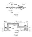
- FIG. 10 is a top plan view of the layout for the tunneling capacitor 124 of FIG. 5D .
- FIG. 5D comprises both an nFET 126 and a pFET 128 fabricated in an isolated p-well 130 , with the two FETs 126 , 128 sharing a single common floating gate 127 / 129 (one plate of the tunneling capacitor) and sharing a common tunneling conductor 131 (the other plate of the tunneling capacitor).
- the two plates of the tunneling capacitor are (1) the shorted floating gates 127 and 129 , typically doped n ⁇ type and p ⁇ type, respectively, for the n ⁇ type and p ⁇ type MOSFETs; and (2) the isolated p ⁇ well 130 , with the nFET's source terminal 131 shorted to the p-well 130 by a conductor 244 , and the pFET's source terminal 137 shorted to the p-well 130 because it forms the ohmic contact for the p ⁇ well (p+ in p ⁇ well).
- the drain terminals 133 and 135 that are butted and shorted (using a silicide in one embodiment) between the nFET 126 and the pFET 128 are also at the same potential as the isolated n ⁇ well 132 and p ⁇ well 130 by reason of the floating-gate nFET or pFET channels being conductive for voltages a few hundred millivolts in either direction from zero on the graph of FIG. 11 .
- FIG. 11 (compare with FIG. 9 ) is a semilog plot of the I-V characteristics of the circuit of FIGS. 5D and 10 .
- the X-axis represents the voltage across the insulator, and the Y-axis represents the absolute value of the tunneling current through the insulator.
- the tunneling current increases by many orders of magnitude as the insulator voltage increases or decreases about zero.
- the region to the left of the zero i.e. gate voltage ⁇ p ⁇ well voltage
- the region to the right of zero i.e.
- the tunneling-current versus insulator-voltage graph of FIG. 11 is also symmetric about zero volts. Because of this inherent symmetry (compare the symmetry in FIG. 11 with the asymmetry in FIG. 9 ), the structure of the device 124 of FIG. 5D is generally considered an improvement over the device 100 of FIG. 5C , although this improvement requires using an additional transistor and additional silicon die area. As in FIG. 9 , the curves computed by modeling and those measured under laboratory conditions are so close together that they could not be distinguished if plotted separately; thus the plot of FIG. 11 represents both.
- FIGS. 12A , 12 B, 12 C; 13 A, 13 B, 13 C; 14 A, 14 B, 14 C; 15 A, 15 B, 15 C; and 16 A, 16 B, 16 C have been expanded and rearranged in order to show all features and entities more clearly. They are not realistic layouts for actual devices, which would be arranged in a considerably more compact form. Also, cross sections of some devices that are aligned up-and-down on the page, rather than across, do not show all of their regions.
- FIGS. 12A , 12 B, and 12 C are, respectively, an electrical schematic diagram, a side elevational cross-sectional drawing, and a top plan view of the layout for a circuit that implements the structure of FIG. 6B , comprising a pFET tunneling capacitor 260 and a four-terminal readout pFET 262 to form a PNVFG charge-storage device in accordance with one embodiment of the present invention.
- the pFET tunneling capacitor 260 has its source 264 , drain 266 , and n ⁇ well 268 all shorted together to comprise one plate of the tunneling capacitor; its floating gate 270 comprises the other plate.
- Both transistors 260 , 262 use gate insulators with oxides sufficiently thin to allow direct electron tunneling.
- Electrons are added to the floating gate 270 by pulling the readout pFET's drain voltage far enough below the floating-gate voltage that electrons tunnel to the floating gate 270 . Electrons are removed from the pFET's floating gate 270 by raising the pFET tunneling-capacitor's n ⁇ well/drain/source voltage (at node 272 ) far enough above the floating-gate voltage that electrons tunnel off the floating gate 270 .
- the readout pFET 262 has a source 274 , drain 276 , well contact 278 and is coupled to floating gate or node 270 .
- Floating gate 270 is insulated from substrate (p ⁇ ) 280 and n ⁇ well 282 by insulators 82 and 84 as disclosed above.
- FIGS. 13A , 13 B, and 13 C are, respectively, an electrical schematic diagram, a side elevational cross-sectional drawing, and a top plan view of the layout for a circuit that implements the basic architecture of FIG. 4C , employing a pFET tunneling capacitor 286 , an nFET tunneling capacitor 288 , and a four-terminal readout pFET 290 to form a PNVFG charge-storage device in accordance with another embodiment of the present invention.
- the pFET tunneling capacitor 286 has its source 292 and drain 294 shorted together to comprise one plate of a tunneling capacitor; the floating gate or floating node 296 comprises the other plate.
- n ⁇ well 295 is brought out separately, and is not shorted to the common node shared by the source 292 and the drain 294 .
- the nFET tunneling capacitor 288 has its source 298 , drain 300 , and well 302 shorted together to comprise one plate of a tunneling capacitor; the floating gate 296 comprises the other plate. Both tunneling capacitors use gate insulators 304 , 306 sufficiently thin to allow direct electron tunneling.
- a four-terminal readout pFET 290 like that illustrated in FIGS.
- Electrons are added to the floating gate 296 by applying a tunneling voltage that is lower than the floating-gate voltage to the shorted source 292 and drain 294 terminals of the pFET tunneling capacitor 286 , causing electrons to tunnel through the gate insulator 304 to the floating gate 296 .
- the n-well 295 may be biased the same as the shorted drain 294 and source 292 terminals, or it may be held at a potential at or above ground.
- pFET tunneling capacitor's drain 294 and source 292 terminals to be biased below ground, without turning on the p-substrate-to-n-well parasitic pn-junction diode. Electrons are removed from the floating gate 296 by applying a tunneling voltage that is higher than the floating-gate voltage to the shorted source 298 , drain 300 , and n-well 302 of the nFET tunneling capacitor 288 , causing electrons to tunnel through the gate insulator 306 off the floating gate 296 .
- Readout pFET 290 has a source 301 , drain 303 and well contact 305 and is disposed in n ⁇ well 307 .
- FIGS. 14A , 14 B, and 14 C are, respectively, an electrical schematic diagram, a side elevational cross-sectional drawing, and a top plan view of the layout for a circuit 320 that implements the circuit of FIG. 7C , comprising a pFET tunneling capacitor 322 and a four-terminal readout nFET 324 to form a PNVFG charge-storage device in accordance with one embodiment of the present invention.
- the readout nFET 324 is fabricated in an isolated p ⁇ well 326 within an n ⁇ well 328 , and so this circuit must be produced in a CMOS process that allows isolated p ⁇ wells. Both transistors use gate insulators 330 , 332 sufficiently thin to allow direct electron tunneling.
- Electrons are added to the floating gate 334 by pulling the readout nFET's source 336 and/or p ⁇ well 338 voltage far enough below the floating-gate voltage that electrons tunnel to the floating gate 334 . Electrons are removed from the floating gate 334 by raising the pFET tunneling capacitor's shorted n-well, source, and drain voltage far enough above the floating-gate voltage that electrons tunnel off the floating gate 334 .
- Readout transistor 324 has an n+ drain contact 325 to which V DD is applied, an n+ source contact 327 to which V INJ is applied, a p+ isolated p ⁇ well contact 329 to which V WELL is applied and an n+ deep n ⁇ well contact 331 to which V DD or ground is applied.
- FIGS. 15A , 15 B, and 15 C are, respectively, an electrical schematic diagram, a side elevational cross-sectional drawing, and a top plan view of the layout for a circuit 340 comprising a pFET tunneling capacitor 342 and a four-terminal readout-and-injection nFET 344 to form a PNVFG charge-storage device in accordance with one embodiment of the present invention.
- the pFET tunneling capacitor 342 uses a gate insulator 346 sufficiently thin to allow direct electron tunneling.
- the readout and injection nFET 344 uses a gate insulator 348 made sufficiently thick that it can accommodate the voltages required for channel-hot-electron injection (CHEI) without incurring insulator damage.
- CHEI channel-hot-electron injection
- the circuit of FIG. 15 has the readout nFET fabricated in substrate rather than in an isolated p-well, and uses CHEI rather than direct tunneling to add electrons to the floating gate 350 . Electrons are added to the floating gate 350 by pulling the readout nFET's drain voltage far enough above its source voltage such that some of its channel electrons, accelerated in the nFET's drain-to-channel depletion region, collide with the semiconductor lattice, scatter upward into the gate insulator, overcome the difference in electron affinities between the semiconductor and the insulator and so enter the insulator's conduction band, and are collected by the floating gate 350 .
- Electrons are removed from the floating gate 350 by raising the pFET tunneling capacitor's shorted n-well, source, and drain voltage (at node 352 ) far enough above the floating-gate voltage that electrons tunnel off the floating gate 350 .
- Many other layout implementations are possible, but are not shown in order to avoid over-complicating the disclosure, such as fabricating the nFET in an isolated p-well; using source-side hot-electron injection to add electrons to the floating gate; or others as will now be apparent to those of ordinary skill in the art.
- FIGS. 16A , 16 B, and 16 C are, respectively, an electrical schematic diagram, a side elevational cross-sectional drawing, and a top plan view of the layout for a circuit 360 comprising a pFET tunneling capacitor 362 and a four-terminal readout-and-injection pFET 364 to form a PNVFG charge-storage device in accordance with one embodiment of the present invention.
- the pFET tunneling capacitor 362 uses a gate insulator 366 sufficiently thin to allow direct electron tunneling.
- the readout and injection pFET 364 uses a gate insulator 368 made sufficiently thick that it can accommodate the voltages required for impact-ionized-hot-electron injection (IHEI) without incurring insulator damage.
- IHEI impact-ionized-hot-electron injection
- the circuit of FIG. 16 uses a readout-and-injection pFET 364 rather than a readout-and-injection nFET 344 , and uses IHEI rather than CHEI to add electrons to the floating gate 368 . Electrons are added to the floating gate 368 by Pulling the readout pFET's drain voltage far enough below its source voltage such that some of its channel holes, accelerated in the pFET's channel-to-drain depletion region, collide with the semiconductor lattice and generate free electrons by means of impact ionization.
- Electrons are removed from the floating gate 368 by raising the pFET tunneling capacitor's shorted n-well, source, and drain voltage at node 370 far enough above the floating-gate voltage that electrons tunnel off the floating gate 368 .
- Many other layout implementations are possible, but are not shown in order to avoid over-complicating the disclosure, such as using a single thin-oxide pFET for both direct tunneling and for IHEI, or others as will now be apparent to those of ordinary skill in the art.
- FIGS. 17A and 17B are, respectively, an electrical schematic diagram of a PNVFG voltage-variable capacitor 380 , and an electrical schematic diagram of a charge-refresh circuit 382 which may be used to update the voltage-variable capacitor's floating-gate charge in, accordance with one embodiment of the present invention.
- the voltage-variable capacitor 380 in FIG. 17A comprises pFETs 384 , 386 , and 388 .
- the pFETs 384 , 386 have gate insulators made sufficiently thicker than the insulator used in pFET 388 , such that negligible tunneling or leakage occurs in or through them.
- the pFET 388 is a tunneling capacitor having a gate oxide sufficiently thin that direct electron tunneling can occur as shown in FIG.
- the capacitance measured from top plate 390 to bottom plate 392 of the voltage-variable capacitor may be varied by adjusting the quantity of charge stored on floating gate 394 .
- the charge refresh circuit 382 of FIG. 17B provides a means of applying tunneling pulses to pFET 388 's shorted source, drain, and well.
- the refresh circuit acts to compare the voltage-variable capacitor with a reference capacitor 396 , whose gate 398 is provided with a reference voltage V REF2 (set equal to the desired floating gate voltage) to set its capacitance value. This comparison is performed as follows: Both the variable capacitor 380 and the reference capacitor 396 are first charged to a reference voltage, V REF1 .
- the amount of charge stored on the two capacitors 380 , 396 is integrated by integrator 400 in a conventional manner and compared against a reference voltage V REF3 at comparator 402 . If the two charge quantities are not equal, a tunneling pulse of proper polarity at the output 404 of comparator 402 will be applied to the shorted source, drain, and well of tunneling capacitor 388 . During refreshing, feedback loop 406 applies these tunneling pulses of polarity +V tun or ⁇ V tun to adjust the quantity of electronic charge stored on floating gate 394 , so that the value of the variable capacitor is set equal to the reference capacitor 396 .
Abstract
Description
Claims (13)
Priority Applications (1)
| Application Number | Priority Date | Filing Date | Title |
|---|---|---|---|
| US11/224,743 US8076707B1 (en) | 2002-05-09 | 2005-09-12 | Pseudo-nonvolatile direct-tunneling floating-gate device |
Applications Claiming Priority (2)
| Application Number | Priority Date | Filing Date | Title |
|---|---|---|---|
| US10/143,557 US20040206999A1 (en) | 2002-05-09 | 2002-05-09 | Metal dielectric semiconductor floating gate variable capacitor |
| US11/224,743 US8076707B1 (en) | 2002-05-09 | 2005-09-12 | Pseudo-nonvolatile direct-tunneling floating-gate device |
Related Parent Applications (1)
| Application Number | Title | Priority Date | Filing Date |
|---|---|---|---|
| US10/143,557 Continuation-In-Part US20040206999A1 (en) | 2002-05-09 | 2002-05-09 | Metal dielectric semiconductor floating gate variable capacitor |
Publications (1)
| Publication Number | Publication Date |
|---|---|
| US8076707B1 true US8076707B1 (en) | 2011-12-13 |
Family
ID=45092666
Family Applications (1)
| Application Number | Title | Priority Date | Filing Date |
|---|---|---|---|
| US11/224,743 Expired - Fee Related US8076707B1 (en) | 2002-05-09 | 2005-09-12 | Pseudo-nonvolatile direct-tunneling floating-gate device |
Country Status (1)
| Country | Link |
|---|---|
| US (1) | US8076707B1 (en) |
Cited By (11)
| Publication number | Priority date | Publication date | Assignee | Title |
|---|---|---|---|---|
| ITTO20120559A1 (en) * | 2012-06-25 | 2013-12-26 | St Microelectronics Srl | NON-VOLATILE MEMORY DEVICE WITH SINGLE-LAYER MEMORY CELLS OF POLYSILIC |
| US8779520B2 (en) | 2012-03-08 | 2014-07-15 | Ememory Technology Inc. | Erasable programmable single-ploy nonvolatile memory |
| EP2811531A1 (en) * | 2013-06-04 | 2014-12-10 | eMemory Technology Inc. | EPROM single-poly memory |
| US20150076564A1 (en) * | 2013-09-17 | 2015-03-19 | Wave Semiconductor, Inc. | Multi-threshold circuitry based on silicon-on-insulator technology |
| US9450052B1 (en) * | 2015-07-01 | 2016-09-20 | Chengdu Monolithic Power Systems Co., Ltd. | EEPROM memory cell with a coupler region and method of making the same |
| US9893207B1 (en) * | 2017-03-17 | 2018-02-13 | International Business Machines Corporation | Programmable read only memory (ROM) integrated in tight pitch vertical transistor structures |
| US10134917B2 (en) * | 2017-03-17 | 2018-11-20 | International Business Machines Corporation | Tight pitch vertical transistor EEPROM |
| US10937746B2 (en) * | 2018-08-31 | 2021-03-02 | Stmicroelectronics (Rousset) Sas | Integrated ultralong time constant time measurement device and fabrication process |
| US11222842B2 (en) * | 2016-08-31 | 2022-01-11 | Taiwan Semiconductor Manufacturing Co., Ltd. | Interconnect structure and methods thereof |
| US11610999B2 (en) * | 2020-06-10 | 2023-03-21 | Globalfoundries Dresden Module One Limited Liability Company & Co. Kg | Floating-gate devices in high voltage applications |
| US20230116512A1 (en) * | 2021-10-11 | 2023-04-13 | Nuvoton Technology Corporation | Method and apparatus for analog floating gate memory cell |
Citations (11)
| Publication number | Priority date | Publication date | Assignee | Title |
|---|---|---|---|---|
| US5511020A (en) * | 1993-11-23 | 1996-04-23 | Monolithic System Technology, Inc. | Pseudo-nonvolatile memory incorporating data refresh operation |
| US5596524A (en) * | 1995-04-21 | 1997-01-21 | Advanced Micro Devices, Inc. | CMOS memory cell with gate oxide of both NMOS and PMOS transistors as tunneling window for program and erase |
| US5627392A (en) | 1995-03-07 | 1997-05-06 | California Institute Of Technology | Semiconductor structure for long term learning |
| US5990512A (en) | 1995-03-07 | 1999-11-23 | California Institute Of Technology | Hole impact ionization mechanism of hot electron injection and four-terminal ρFET semiconductor structure for long-term learning |
| US6091657A (en) * | 1999-01-20 | 2000-07-18 | Lucent Technologies Inc. | Integrated circuit having protection of low voltage devices |
| US6137153A (en) * | 1998-02-13 | 2000-10-24 | Advanced Micro Devices, Inc. | Floating gate capacitor for use in voltage regulators |
| US6274898B1 (en) * | 1999-05-21 | 2001-08-14 | Vantis Corporation | Triple-well EEPROM cell using P-well for tunneling across a channel |
| US6678190B2 (en) | 2002-01-25 | 2004-01-13 | Ememory Technology Inc. | Single poly embedded eprom |
| US20040206999A1 (en) * | 2002-05-09 | 2004-10-21 | Impinj, Inc., A Delaware Corporation | Metal dielectric semiconductor floating gate variable capacitor |
| US6965142B2 (en) * | 1995-03-07 | 2005-11-15 | Impinj, Inc. | Floating-gate semiconductor structures |
| US6985387B2 (en) * | 2000-12-20 | 2006-01-10 | Broadcom Corporation | System and method for one-time programmed memory through direct-tunneling oxide breakdown |
-
2005
- 2005-09-12 US US11/224,743 patent/US8076707B1/en not_active Expired - Fee Related
Patent Citations (11)
| Publication number | Priority date | Publication date | Assignee | Title |
|---|---|---|---|---|
| US5511020A (en) * | 1993-11-23 | 1996-04-23 | Monolithic System Technology, Inc. | Pseudo-nonvolatile memory incorporating data refresh operation |
| US5627392A (en) | 1995-03-07 | 1997-05-06 | California Institute Of Technology | Semiconductor structure for long term learning |
| US5990512A (en) | 1995-03-07 | 1999-11-23 | California Institute Of Technology | Hole impact ionization mechanism of hot electron injection and four-terminal ρFET semiconductor structure for long-term learning |
| US6965142B2 (en) * | 1995-03-07 | 2005-11-15 | Impinj, Inc. | Floating-gate semiconductor structures |
| US5596524A (en) * | 1995-04-21 | 1997-01-21 | Advanced Micro Devices, Inc. | CMOS memory cell with gate oxide of both NMOS and PMOS transistors as tunneling window for program and erase |
| US6137153A (en) * | 1998-02-13 | 2000-10-24 | Advanced Micro Devices, Inc. | Floating gate capacitor for use in voltage regulators |
| US6091657A (en) * | 1999-01-20 | 2000-07-18 | Lucent Technologies Inc. | Integrated circuit having protection of low voltage devices |
| US6274898B1 (en) * | 1999-05-21 | 2001-08-14 | Vantis Corporation | Triple-well EEPROM cell using P-well for tunneling across a channel |
| US6985387B2 (en) * | 2000-12-20 | 2006-01-10 | Broadcom Corporation | System and method for one-time programmed memory through direct-tunneling oxide breakdown |
| US6678190B2 (en) | 2002-01-25 | 2004-01-13 | Ememory Technology Inc. | Single poly embedded eprom |
| US20040206999A1 (en) * | 2002-05-09 | 2004-10-21 | Impinj, Inc., A Delaware Corporation | Metal dielectric semiconductor floating gate variable capacitor |
Non-Patent Citations (1)
| Title |
|---|
| Tatsuya Usuki, et al., "Direct Tunneling Memory: Trade-off Between Nonvolatility and High Endurance with Low Voltage Operations", Nonvolatile Semiconductor Workshop Symposium, Aug. 12, 2001, pp. 80-81. |
Cited By (14)
| Publication number | Priority date | Publication date | Assignee | Title |
|---|---|---|---|---|
| US8779520B2 (en) | 2012-03-08 | 2014-07-15 | Ememory Technology Inc. | Erasable programmable single-ploy nonvolatile memory |
| ITTO20120559A1 (en) * | 2012-06-25 | 2013-12-26 | St Microelectronics Srl | NON-VOLATILE MEMORY DEVICE WITH SINGLE-LAYER MEMORY CELLS OF POLYSILIC |
| US8873291B2 (en) | 2012-06-25 | 2014-10-28 | Stmicroelectronics S.R.L. | Non-volatile memory device with single-polysilicon-layer memory cells |
| EP2811531A1 (en) * | 2013-06-04 | 2014-12-10 | eMemory Technology Inc. | EPROM single-poly memory |
| US20150076564A1 (en) * | 2013-09-17 | 2015-03-19 | Wave Semiconductor, Inc. | Multi-threshold circuitry based on silicon-on-insulator technology |
| US9257984B2 (en) * | 2013-09-17 | 2016-02-09 | Wave Semiconductor, Inc. | Multi-threshold circuitry based on silicon-on-insulator technology |
| US9450052B1 (en) * | 2015-07-01 | 2016-09-20 | Chengdu Monolithic Power Systems Co., Ltd. | EEPROM memory cell with a coupler region and method of making the same |
| US11222842B2 (en) * | 2016-08-31 | 2022-01-11 | Taiwan Semiconductor Manufacturing Co., Ltd. | Interconnect structure and methods thereof |
| US9893207B1 (en) * | 2017-03-17 | 2018-02-13 | International Business Machines Corporation | Programmable read only memory (ROM) integrated in tight pitch vertical transistor structures |
| US10134917B2 (en) * | 2017-03-17 | 2018-11-20 | International Business Machines Corporation | Tight pitch vertical transistor EEPROM |
| US10937746B2 (en) * | 2018-08-31 | 2021-03-02 | Stmicroelectronics (Rousset) Sas | Integrated ultralong time constant time measurement device and fabrication process |
| US11721646B2 (en) | 2018-08-31 | 2023-08-08 | Stmicroelectronics (Rousset) Sas | Integrated ultralong time constant time measurement device and fabrication process |
| US11610999B2 (en) * | 2020-06-10 | 2023-03-21 | Globalfoundries Dresden Module One Limited Liability Company & Co. Kg | Floating-gate devices in high voltage applications |
| US20230116512A1 (en) * | 2021-10-11 | 2023-04-13 | Nuvoton Technology Corporation | Method and apparatus for analog floating gate memory cell |
Similar Documents
| Publication | Publication Date | Title |
|---|---|---|
| US20040021166A1 (en) | Pseudo-nonvolatile direct-tunneling floating-gate device | |
| US8076707B1 (en) | Pseudo-nonvolatile direct-tunneling floating-gate device | |
| US7098498B2 (en) | Floating-gate semiconductor structures | |
| US7741177B2 (en) | Method and apparatus transporting charges in semiconductor device and semiconductor memory device | |
| US7750395B2 (en) | Scalable Flash/NV structures and devices with extended endurance | |
| US6950340B2 (en) | Asymmetric band-gap engineered nonvolatile memory device | |
| US7728626B2 (en) | Memory utilizing oxide nanolaminates | |
| US7297634B2 (en) | Method and apparatus for semiconductor device and semiconductor memory device | |
| EP0573164B1 (en) | Full feature high density EEPROM cell with poly tunnel spacer and method of manufacture | |
| JPH09185891A (en) | Nonvolatile memory cell having single poly-silicon gate | |
| US7570521B2 (en) | Low power flash memory devices | |
| US20060220096A1 (en) | Tunneling-enhanced floating gate semiconductor device | |
| WO2003096432A1 (en) | Pseudo-nonvolatile direct-tunneling floating-gate device | |
| US5589700A (en) | Semiconductor nonvolatile memory | |
| JP2001185633A (en) | Eeprom device | |
| US7613041B2 (en) | Methods for operating semiconductor device and semiconductor memory device | |
| US5508955A (en) | Electronically erasable-programmable memory cell having buried bit line | |
| US20060226489A1 (en) | System and methods for retention-enhanced programmable shared gate logic circuit |
Legal Events
| Date | Code | Title | Description |
|---|---|---|---|
| AS | Assignment |
Owner name: IMPINJ, INC., WASHINGTON Free format text: ASSIGNMENT OF ASSIGNORS INTEREST;ASSIGNORS:HYDE, JOHN D.;HUMES, TODD E.;DIORIO, CHRISTOPHER J.;AND OTHERS;SIGNING DATES FROM 20030602 TO 20050531;REEL/FRAME:019120/0173 |
|
| AS | Assignment |
Owner name: VIRAGE LOGIC CORPORATION, CALIFORNIA Free format text: ASSIGNMENT OF ASSIGNORS INTEREST;ASSIGNOR:IMPINJ, INC.;REEL/FRAME:021637/0351 Effective date: 20080625 |
|
| AS | Assignment |
Owner name: SYNOPSYS, INC., CALIFORNIA Free format text: ASSIGNMENT OF ASSIGNORS INTEREST;ASSIGNORS:VIRAGE LOGIC CORPORATION;VL C.V.;ARC CORES LIMITED;AND OTHERS;REEL/FRAME:025105/0907 Effective date: 20100902 |
|
| ZAAA | Notice of allowance and fees due |
Free format text: ORIGINAL CODE: NOA |
|
| ZAAB | Notice of allowance mailed |
Free format text: ORIGINAL CODE: MN/=. |
|
| STCF | Information on status: patent grant |
Free format text: PATENTED CASE |
|
| FPAY | Fee payment |
Year of fee payment: 4 |
|
| MAFP | Maintenance fee payment |
Free format text: PAYMENT OF MAINTENANCE FEE, 8TH YEAR, LARGE ENTITY (ORIGINAL EVENT CODE: M1552); ENTITY STATUS OF PATENT OWNER: LARGE ENTITY Year of fee payment: 8 |
|
| FEPP | Fee payment procedure |
Free format text: MAINTENANCE FEE REMINDER MAILED (ORIGINAL EVENT CODE: REM.); ENTITY STATUS OF PATENT OWNER: LARGE ENTITY |
|
| LAPS | Lapse for failure to pay maintenance fees |
Free format text: PATENT EXPIRED FOR FAILURE TO PAY MAINTENANCE FEES (ORIGINAL EVENT CODE: EXP.); ENTITY STATUS OF PATENT OWNER: LARGE ENTITY |
|
| STCH | Information on status: patent discontinuation |
Free format text: PATENT EXPIRED DUE TO NONPAYMENT OF MAINTENANCE FEES UNDER 37 CFR 1.362 |
|
| FP | Lapsed due to failure to pay maintenance fee |
Effective date: 20231213 |