US8089159B1 - Semiconductor package with increased I/O density and method of making the same - Google Patents
Semiconductor package with increased I/O density and method of making the same Download PDFInfo
- Publication number
- US8089159B1 US8089159B1 US11/866,886 US86688607A US8089159B1 US 8089159 B1 US8089159 B1 US 8089159B1 US 86688607 A US86688607 A US 86688607A US 8089159 B1 US8089159 B1 US 8089159B1
- Authority
- US
- United States
- Prior art keywords
- pads
- pad
- ring
- plated
- die
- Prior art date
- Legal status (The legal status is an assumption and is not a legal conclusion. Google has not performed a legal analysis and makes no representation as to the accuracy of the status listed.)
- Active, expires
Links
Images


Classifications
-
- H—ELECTRICITY
- H01—ELECTRIC ELEMENTS
- H01L—SEMICONDUCTOR DEVICES NOT COVERED BY CLASS H10
- H01L24/00—Arrangements for connecting or disconnecting semiconductor or solid-state bodies; Methods or apparatus related thereto
- H01L24/93—Batch processes
- H01L24/95—Batch processes at chip-level, i.e. with connecting carried out on a plurality of singulated devices, i.e. on diced chips
- H01L24/97—Batch processes at chip-level, i.e. with connecting carried out on a plurality of singulated devices, i.e. on diced chips the devices being connected to a common substrate, e.g. interposer, said common substrate being separable into individual assemblies after connecting
-
- H—ELECTRICITY
- H01—ELECTRIC ELEMENTS
- H01L—SEMICONDUCTOR DEVICES NOT COVERED BY CLASS H10
- H01L21/00—Processes or apparatus adapted for the manufacture or treatment of semiconductor or solid state devices or of parts thereof
- H01L21/02—Manufacture or treatment of semiconductor devices or of parts thereof
- H01L21/04—Manufacture or treatment of semiconductor devices or of parts thereof the devices having at least one potential-jump barrier or surface barrier, e.g. PN junction, depletion layer or carrier concentration layer
- H01L21/48—Manufacture or treatment of parts, e.g. containers, prior to assembly of the devices, using processes not provided for in a single one of the subgroups H01L21/06 - H01L21/326
- H01L21/4814—Conductive parts
- H01L21/4821—Flat leads, e.g. lead frames with or without insulating supports
- H01L21/4828—Etching
- H01L21/4832—Etching a temporary substrate after encapsulation process to form leads
-
- H—ELECTRICITY
- H01—ELECTRIC ELEMENTS
- H01L—SEMICONDUCTOR DEVICES NOT COVERED BY CLASS H10
- H01L21/00—Processes or apparatus adapted for the manufacture or treatment of semiconductor or solid state devices or of parts thereof
- H01L21/02—Manufacture or treatment of semiconductor devices or of parts thereof
- H01L21/04—Manufacture or treatment of semiconductor devices or of parts thereof the devices having at least one potential-jump barrier or surface barrier, e.g. PN junction, depletion layer or carrier concentration layer
- H01L21/50—Assembly of semiconductor devices using processes or apparatus not provided for in a single one of the subgroups H01L21/06 - H01L21/326, e.g. sealing of a cap to a base of a container
- H01L21/56—Encapsulations, e.g. encapsulation layers, coatings
- H01L21/561—Batch processing
-
- H—ELECTRICITY
- H01—ELECTRIC ELEMENTS
- H01L—SEMICONDUCTOR DEVICES NOT COVERED BY CLASS H10
- H01L21/00—Processes or apparatus adapted for the manufacture or treatment of semiconductor or solid state devices or of parts thereof
- H01L21/02—Manufacture or treatment of semiconductor devices or of parts thereof
- H01L21/04—Manufacture or treatment of semiconductor devices or of parts thereof the devices having at least one potential-jump barrier or surface barrier, e.g. PN junction, depletion layer or carrier concentration layer
- H01L21/50—Assembly of semiconductor devices using processes or apparatus not provided for in a single one of the subgroups H01L21/06 - H01L21/326, e.g. sealing of a cap to a base of a container
- H01L21/56—Encapsulations, e.g. encapsulation layers, coatings
- H01L21/565—Moulds
-
- H—ELECTRICITY
- H01—ELECTRIC ELEMENTS
- H01L—SEMICONDUCTOR DEVICES NOT COVERED BY CLASS H10
- H01L21/00—Processes or apparatus adapted for the manufacture or treatment of semiconductor or solid state devices or of parts thereof
- H01L21/02—Manufacture or treatment of semiconductor devices or of parts thereof
- H01L21/04—Manufacture or treatment of semiconductor devices or of parts thereof the devices having at least one potential-jump barrier or surface barrier, e.g. PN junction, depletion layer or carrier concentration layer
- H01L21/50—Assembly of semiconductor devices using processes or apparatus not provided for in a single one of the subgroups H01L21/06 - H01L21/326, e.g. sealing of a cap to a base of a container
- H01L21/56—Encapsulations, e.g. encapsulation layers, coatings
- H01L21/568—Temporary substrate used as encapsulation process aid
-
- H—ELECTRICITY
- H01—ELECTRIC ELEMENTS
- H01L—SEMICONDUCTOR DEVICES NOT COVERED BY CLASS H10
- H01L23/00—Details of semiconductor or other solid state devices
- H01L23/28—Encapsulations, e.g. encapsulating layers, coatings, e.g. for protection
- H01L23/31—Encapsulations, e.g. encapsulating layers, coatings, e.g. for protection characterised by the arrangement or shape
- H01L23/3107—Encapsulations, e.g. encapsulating layers, coatings, e.g. for protection characterised by the arrangement or shape the device being completely enclosed
-
- H—ELECTRICITY
- H01—ELECTRIC ELEMENTS
- H01L—SEMICONDUCTOR DEVICES NOT COVERED BY CLASS H10
- H01L23/00—Details of semiconductor or other solid state devices
- H01L23/48—Arrangements for conducting electric current to or from the solid state body in operation, e.g. leads, terminal arrangements ; Selection of materials therefor
- H01L23/488—Arrangements for conducting electric current to or from the solid state body in operation, e.g. leads, terminal arrangements ; Selection of materials therefor consisting of soldered or bonded constructions
- H01L23/495—Lead-frames or other flat leads
- H01L23/49541—Geometry of the lead-frame
-
- H—ELECTRICITY
- H01—ELECTRIC ELEMENTS
- H01L—SEMICONDUCTOR DEVICES NOT COVERED BY CLASS H10
- H01L23/00—Details of semiconductor or other solid state devices
- H01L23/48—Arrangements for conducting electric current to or from the solid state body in operation, e.g. leads, terminal arrangements ; Selection of materials therefor
- H01L23/488—Arrangements for conducting electric current to or from the solid state body in operation, e.g. leads, terminal arrangements ; Selection of materials therefor consisting of soldered or bonded constructions
- H01L23/495—Lead-frames or other flat leads
- H01L23/49579—Lead-frames or other flat leads characterised by the materials of the lead frames or layers thereon
- H01L23/49582—Metallic layers on lead frames
-
- H—ELECTRICITY
- H01—ELECTRIC ELEMENTS
- H01L—SEMICONDUCTOR DEVICES NOT COVERED BY CLASS H10
- H01L24/00—Arrangements for connecting or disconnecting semiconductor or solid-state bodies; Methods or apparatus related thereto
- H01L24/01—Means for bonding being attached to, or being formed on, the surface to be connected, e.g. chip-to-package, die-attach, "first-level" interconnects; Manufacturing methods related thereto
- H01L24/10—Bump connectors ; Manufacturing methods related thereto
- H01L24/12—Structure, shape, material or disposition of the bump connectors prior to the connecting process
- H01L24/13—Structure, shape, material or disposition of the bump connectors prior to the connecting process of an individual bump connector
-
- H—ELECTRICITY
- H01—ELECTRIC ELEMENTS
- H01L—SEMICONDUCTOR DEVICES NOT COVERED BY CLASS H10
- H01L24/00—Arrangements for connecting or disconnecting semiconductor or solid-state bodies; Methods or apparatus related thereto
- H01L24/01—Means for bonding being attached to, or being formed on, the surface to be connected, e.g. chip-to-package, die-attach, "first-level" interconnects; Manufacturing methods related thereto
- H01L24/10—Bump connectors ; Manufacturing methods related thereto
- H01L24/15—Structure, shape, material or disposition of the bump connectors after the connecting process
- H01L24/16—Structure, shape, material or disposition of the bump connectors after the connecting process of an individual bump connector
-
- H—ELECTRICITY
- H01—ELECTRIC ELEMENTS
- H01L—SEMICONDUCTOR DEVICES NOT COVERED BY CLASS H10
- H01L24/00—Arrangements for connecting or disconnecting semiconductor or solid-state bodies; Methods or apparatus related thereto
- H01L24/01—Means for bonding being attached to, or being formed on, the surface to be connected, e.g. chip-to-package, die-attach, "first-level" interconnects; Manufacturing methods related thereto
- H01L24/42—Wire connectors; Manufacturing methods related thereto
- H01L24/47—Structure, shape, material or disposition of the wire connectors after the connecting process
- H01L24/49—Structure, shape, material or disposition of the wire connectors after the connecting process of a plurality of wire connectors
-
- H—ELECTRICITY
- H01—ELECTRIC ELEMENTS
- H01L—SEMICONDUCTOR DEVICES NOT COVERED BY CLASS H10
- H01L24/00—Arrangements for connecting or disconnecting semiconductor or solid-state bodies; Methods or apparatus related thereto
- H01L24/80—Methods for connecting semiconductor or other solid state bodies using means for bonding being attached to, or being formed on, the surface to be connected
- H01L24/81—Methods for connecting semiconductor or other solid state bodies using means for bonding being attached to, or being formed on, the surface to be connected using a bump connector
-
- H—ELECTRICITY
- H01—ELECTRIC ELEMENTS
- H01L—SEMICONDUCTOR DEVICES NOT COVERED BY CLASS H10
- H01L24/00—Arrangements for connecting or disconnecting semiconductor or solid-state bodies; Methods or apparatus related thereto
- H01L24/80—Methods for connecting semiconductor or other solid state bodies using means for bonding being attached to, or being formed on, the surface to be connected
- H01L24/83—Methods for connecting semiconductor or other solid state bodies using means for bonding being attached to, or being formed on, the surface to be connected using a layer connector
-
- H—ELECTRICITY
- H01—ELECTRIC ELEMENTS
- H01L—SEMICONDUCTOR DEVICES NOT COVERED BY CLASS H10
- H01L24/00—Arrangements for connecting or disconnecting semiconductor or solid-state bodies; Methods or apparatus related thereto
- H01L24/80—Methods for connecting semiconductor or other solid state bodies using means for bonding being attached to, or being formed on, the surface to be connected
- H01L24/85—Methods for connecting semiconductor or other solid state bodies using means for bonding being attached to, or being formed on, the surface to be connected using a wire connector
-
- H—ELECTRICITY
- H01—ELECTRIC ELEMENTS
- H01L—SEMICONDUCTOR DEVICES NOT COVERED BY CLASS H10
- H01L2224/00—Indexing scheme for arrangements for connecting or disconnecting semiconductor or solid-state bodies and methods related thereto as covered by H01L24/00
- H01L2224/01—Means for bonding being attached to, or being formed on, the surface to be connected, e.g. chip-to-package, die-attach, "first-level" interconnects; Manufacturing methods related thereto
- H01L2224/10—Bump connectors; Manufacturing methods related thereto
- H01L2224/12—Structure, shape, material or disposition of the bump connectors prior to the connecting process
- H01L2224/13—Structure, shape, material or disposition of the bump connectors prior to the connecting process of an individual bump connector
- H01L2224/13001—Core members of the bump connector
- H01L2224/13099—Material
- H01L2224/131—Material with a principal constituent of the material being a metal or a metalloid, e.g. boron [B], silicon [Si], germanium [Ge], arsenic [As], antimony [Sb], tellurium [Te] and polonium [Po], and alloys thereof
- H01L2224/13138—Material with a principal constituent of the material being a metal or a metalloid, e.g. boron [B], silicon [Si], germanium [Ge], arsenic [As], antimony [Sb], tellurium [Te] and polonium [Po], and alloys thereof the principal constituent melting at a temperature of greater than or equal to 950°C and less than 1550°C
- H01L2224/13139—Silver [Ag] as principal constituent
-
- H—ELECTRICITY
- H01—ELECTRIC ELEMENTS
- H01L—SEMICONDUCTOR DEVICES NOT COVERED BY CLASS H10
- H01L2224/00—Indexing scheme for arrangements for connecting or disconnecting semiconductor or solid-state bodies and methods related thereto as covered by H01L24/00
- H01L2224/01—Means for bonding being attached to, or being formed on, the surface to be connected, e.g. chip-to-package, die-attach, "first-level" interconnects; Manufacturing methods related thereto
- H01L2224/10—Bump connectors; Manufacturing methods related thereto
- H01L2224/12—Structure, shape, material or disposition of the bump connectors prior to the connecting process
- H01L2224/13—Structure, shape, material or disposition of the bump connectors prior to the connecting process of an individual bump connector
- H01L2224/13001—Core members of the bump connector
- H01L2224/13099—Material
- H01L2224/131—Material with a principal constituent of the material being a metal or a metalloid, e.g. boron [B], silicon [Si], germanium [Ge], arsenic [As], antimony [Sb], tellurium [Te] and polonium [Po], and alloys thereof
- H01L2224/13138—Material with a principal constituent of the material being a metal or a metalloid, e.g. boron [B], silicon [Si], germanium [Ge], arsenic [As], antimony [Sb], tellurium [Te] and polonium [Po], and alloys thereof the principal constituent melting at a temperature of greater than or equal to 950°C and less than 1550°C
- H01L2224/13144—Gold [Au] as principal constituent
-
- H—ELECTRICITY
- H01—ELECTRIC ELEMENTS
- H01L—SEMICONDUCTOR DEVICES NOT COVERED BY CLASS H10
- H01L2224/00—Indexing scheme for arrangements for connecting or disconnecting semiconductor or solid-state bodies and methods related thereto as covered by H01L24/00
- H01L2224/01—Means for bonding being attached to, or being formed on, the surface to be connected, e.g. chip-to-package, die-attach, "first-level" interconnects; Manufacturing methods related thereto
- H01L2224/10—Bump connectors; Manufacturing methods related thereto
- H01L2224/15—Structure, shape, material or disposition of the bump connectors after the connecting process
- H01L2224/16—Structure, shape, material or disposition of the bump connectors after the connecting process of an individual bump connector
- H01L2224/161—Disposition
- H01L2224/16151—Disposition the bump connector connecting between a semiconductor or solid-state body and an item not being a semiconductor or solid-state body, e.g. chip-to-substrate, chip-to-passive
- H01L2224/16221—Disposition the bump connector connecting between a semiconductor or solid-state body and an item not being a semiconductor or solid-state body, e.g. chip-to-substrate, chip-to-passive the body and the item being stacked
- H01L2224/16245—Disposition the bump connector connecting between a semiconductor or solid-state body and an item not being a semiconductor or solid-state body, e.g. chip-to-substrate, chip-to-passive the body and the item being stacked the item being metallic
-
- H—ELECTRICITY
- H01—ELECTRIC ELEMENTS
- H01L—SEMICONDUCTOR DEVICES NOT COVERED BY CLASS H10
- H01L2224/00—Indexing scheme for arrangements for connecting or disconnecting semiconductor or solid-state bodies and methods related thereto as covered by H01L24/00
- H01L2224/01—Means for bonding being attached to, or being formed on, the surface to be connected, e.g. chip-to-package, die-attach, "first-level" interconnects; Manufacturing methods related thereto
- H01L2224/26—Layer connectors, e.g. plate connectors, solder or adhesive layers; Manufacturing methods related thereto
- H01L2224/28—Structure, shape, material or disposition of the layer connectors prior to the connecting process
- H01L2224/29—Structure, shape, material or disposition of the layer connectors prior to the connecting process of an individual layer connector
- H01L2224/29001—Core members of the layer connector
- H01L2224/29099—Material
- H01L2224/2919—Material with a principal constituent of the material being a polymer, e.g. polyester, phenolic based polymer, epoxy
-
- H—ELECTRICITY
- H01—ELECTRIC ELEMENTS
- H01L—SEMICONDUCTOR DEVICES NOT COVERED BY CLASS H10
- H01L2224/00—Indexing scheme for arrangements for connecting or disconnecting semiconductor or solid-state bodies and methods related thereto as covered by H01L24/00
- H01L2224/01—Means for bonding being attached to, or being formed on, the surface to be connected, e.g. chip-to-package, die-attach, "first-level" interconnects; Manufacturing methods related thereto
- H01L2224/26—Layer connectors, e.g. plate connectors, solder or adhesive layers; Manufacturing methods related thereto
- H01L2224/31—Structure, shape, material or disposition of the layer connectors after the connecting process
- H01L2224/32—Structure, shape, material or disposition of the layer connectors after the connecting process of an individual layer connector
- H01L2224/321—Disposition
- H01L2224/32151—Disposition the layer connector connecting between a semiconductor or solid-state body and an item not being a semiconductor or solid-state body, e.g. chip-to-substrate, chip-to-passive
- H01L2224/32221—Disposition the layer connector connecting between a semiconductor or solid-state body and an item not being a semiconductor or solid-state body, e.g. chip-to-substrate, chip-to-passive the body and the item being stacked
- H01L2224/32245—Disposition the layer connector connecting between a semiconductor or solid-state body and an item not being a semiconductor or solid-state body, e.g. chip-to-substrate, chip-to-passive the body and the item being stacked the item being metallic
-
- H—ELECTRICITY
- H01—ELECTRIC ELEMENTS
- H01L—SEMICONDUCTOR DEVICES NOT COVERED BY CLASS H10
- H01L2224/00—Indexing scheme for arrangements for connecting or disconnecting semiconductor or solid-state bodies and methods related thereto as covered by H01L24/00
- H01L2224/01—Means for bonding being attached to, or being formed on, the surface to be connected, e.g. chip-to-package, die-attach, "first-level" interconnects; Manufacturing methods related thereto
- H01L2224/42—Wire connectors; Manufacturing methods related thereto
- H01L2224/44—Structure, shape, material or disposition of the wire connectors prior to the connecting process
- H01L2224/45—Structure, shape, material or disposition of the wire connectors prior to the connecting process of an individual wire connector
- H01L2224/45001—Core members of the connector
- H01L2224/45099—Material
- H01L2224/451—Material with a principal constituent of the material being a metal or a metalloid, e.g. boron (B), silicon (Si), germanium (Ge), arsenic (As), antimony (Sb), tellurium (Te) and polonium (Po), and alloys thereof
- H01L2224/45117—Material with a principal constituent of the material being a metal or a metalloid, e.g. boron (B), silicon (Si), germanium (Ge), arsenic (As), antimony (Sb), tellurium (Te) and polonium (Po), and alloys thereof the principal constituent melting at a temperature of greater than or equal to 400°C and less than 950°C
- H01L2224/45124—Aluminium (Al) as principal constituent
-
- H—ELECTRICITY
- H01—ELECTRIC ELEMENTS
- H01L—SEMICONDUCTOR DEVICES NOT COVERED BY CLASS H10
- H01L2224/00—Indexing scheme for arrangements for connecting or disconnecting semiconductor or solid-state bodies and methods related thereto as covered by H01L24/00
- H01L2224/01—Means for bonding being attached to, or being formed on, the surface to be connected, e.g. chip-to-package, die-attach, "first-level" interconnects; Manufacturing methods related thereto
- H01L2224/42—Wire connectors; Manufacturing methods related thereto
- H01L2224/44—Structure, shape, material or disposition of the wire connectors prior to the connecting process
- H01L2224/45—Structure, shape, material or disposition of the wire connectors prior to the connecting process of an individual wire connector
- H01L2224/45001—Core members of the connector
- H01L2224/45099—Material
- H01L2224/451—Material with a principal constituent of the material being a metal or a metalloid, e.g. boron (B), silicon (Si), germanium (Ge), arsenic (As), antimony (Sb), tellurium (Te) and polonium (Po), and alloys thereof
- H01L2224/45138—Material with a principal constituent of the material being a metal or a metalloid, e.g. boron (B), silicon (Si), germanium (Ge), arsenic (As), antimony (Sb), tellurium (Te) and polonium (Po), and alloys thereof the principal constituent melting at a temperature of greater than or equal to 950°C and less than 1550°C
- H01L2224/45144—Gold (Au) as principal constituent
-
- H—ELECTRICITY
- H01—ELECTRIC ELEMENTS
- H01L—SEMICONDUCTOR DEVICES NOT COVERED BY CLASS H10
- H01L2224/00—Indexing scheme for arrangements for connecting or disconnecting semiconductor or solid-state bodies and methods related thereto as covered by H01L24/00
- H01L2224/01—Means for bonding being attached to, or being formed on, the surface to be connected, e.g. chip-to-package, die-attach, "first-level" interconnects; Manufacturing methods related thereto
- H01L2224/42—Wire connectors; Manufacturing methods related thereto
- H01L2224/44—Structure, shape, material or disposition of the wire connectors prior to the connecting process
- H01L2224/45—Structure, shape, material or disposition of the wire connectors prior to the connecting process of an individual wire connector
- H01L2224/45001—Core members of the connector
- H01L2224/45099—Material
- H01L2224/451—Material with a principal constituent of the material being a metal or a metalloid, e.g. boron (B), silicon (Si), germanium (Ge), arsenic (As), antimony (Sb), tellurium (Te) and polonium (Po), and alloys thereof
- H01L2224/45138—Material with a principal constituent of the material being a metal or a metalloid, e.g. boron (B), silicon (Si), germanium (Ge), arsenic (As), antimony (Sb), tellurium (Te) and polonium (Po), and alloys thereof the principal constituent melting at a temperature of greater than or equal to 950°C and less than 1550°C
- H01L2224/45147—Copper (Cu) as principal constituent
-
- H—ELECTRICITY
- H01—ELECTRIC ELEMENTS
- H01L—SEMICONDUCTOR DEVICES NOT COVERED BY CLASS H10
- H01L2224/00—Indexing scheme for arrangements for connecting or disconnecting semiconductor or solid-state bodies and methods related thereto as covered by H01L24/00
- H01L2224/01—Means for bonding being attached to, or being formed on, the surface to be connected, e.g. chip-to-package, die-attach, "first-level" interconnects; Manufacturing methods related thereto
- H01L2224/42—Wire connectors; Manufacturing methods related thereto
- H01L2224/47—Structure, shape, material or disposition of the wire connectors after the connecting process
- H01L2224/48—Structure, shape, material or disposition of the wire connectors after the connecting process of an individual wire connector
- H01L2224/4805—Shape
- H01L2224/4809—Loop shape
- H01L2224/48091—Arched
-
- H—ELECTRICITY
- H01—ELECTRIC ELEMENTS
- H01L—SEMICONDUCTOR DEVICES NOT COVERED BY CLASS H10
- H01L2224/00—Indexing scheme for arrangements for connecting or disconnecting semiconductor or solid-state bodies and methods related thereto as covered by H01L24/00
- H01L2224/01—Means for bonding being attached to, or being formed on, the surface to be connected, e.g. chip-to-package, die-attach, "first-level" interconnects; Manufacturing methods related thereto
- H01L2224/42—Wire connectors; Manufacturing methods related thereto
- H01L2224/47—Structure, shape, material or disposition of the wire connectors after the connecting process
- H01L2224/48—Structure, shape, material or disposition of the wire connectors after the connecting process of an individual wire connector
- H01L2224/481—Disposition
- H01L2224/48151—Connecting between a semiconductor or solid-state body and an item not being a semiconductor or solid-state body, e.g. chip-to-substrate, chip-to-passive
- H01L2224/48221—Connecting between a semiconductor or solid-state body and an item not being a semiconductor or solid-state body, e.g. chip-to-substrate, chip-to-passive the body and the item being stacked
- H01L2224/48245—Connecting between a semiconductor or solid-state body and an item not being a semiconductor or solid-state body, e.g. chip-to-substrate, chip-to-passive the body and the item being stacked the item being metallic
- H01L2224/48247—Connecting between a semiconductor or solid-state body and an item not being a semiconductor or solid-state body, e.g. chip-to-substrate, chip-to-passive the body and the item being stacked the item being metallic connecting the wire to a bond pad of the item
-
- H—ELECTRICITY
- H01—ELECTRIC ELEMENTS
- H01L—SEMICONDUCTOR DEVICES NOT COVERED BY CLASS H10
- H01L2224/00—Indexing scheme for arrangements for connecting or disconnecting semiconductor or solid-state bodies and methods related thereto as covered by H01L24/00
- H01L2224/01—Means for bonding being attached to, or being formed on, the surface to be connected, e.g. chip-to-package, die-attach, "first-level" interconnects; Manufacturing methods related thereto
- H01L2224/42—Wire connectors; Manufacturing methods related thereto
- H01L2224/47—Structure, shape, material or disposition of the wire connectors after the connecting process
- H01L2224/48—Structure, shape, material or disposition of the wire connectors after the connecting process of an individual wire connector
- H01L2224/481—Disposition
- H01L2224/48151—Connecting between a semiconductor or solid-state body and an item not being a semiconductor or solid-state body, e.g. chip-to-substrate, chip-to-passive
- H01L2224/48221—Connecting between a semiconductor or solid-state body and an item not being a semiconductor or solid-state body, e.g. chip-to-substrate, chip-to-passive the body and the item being stacked
- H01L2224/48245—Connecting between a semiconductor or solid-state body and an item not being a semiconductor or solid-state body, e.g. chip-to-substrate, chip-to-passive the body and the item being stacked the item being metallic
- H01L2224/48257—Connecting between a semiconductor or solid-state body and an item not being a semiconductor or solid-state body, e.g. chip-to-substrate, chip-to-passive the body and the item being stacked the item being metallic connecting the wire to a die pad of the item
-
- H—ELECTRICITY
- H01—ELECTRIC ELEMENTS
- H01L—SEMICONDUCTOR DEVICES NOT COVERED BY CLASS H10
- H01L2224/00—Indexing scheme for arrangements for connecting or disconnecting semiconductor or solid-state bodies and methods related thereto as covered by H01L24/00
- H01L2224/01—Means for bonding being attached to, or being formed on, the surface to be connected, e.g. chip-to-package, die-attach, "first-level" interconnects; Manufacturing methods related thereto
- H01L2224/42—Wire connectors; Manufacturing methods related thereto
- H01L2224/47—Structure, shape, material or disposition of the wire connectors after the connecting process
- H01L2224/48—Structure, shape, material or disposition of the wire connectors after the connecting process of an individual wire connector
- H01L2224/484—Connecting portions
- H01L2224/48463—Connecting portions the connecting portion on the bonding area of the semiconductor or solid-state body being a ball bond
- H01L2224/48465—Connecting portions the connecting portion on the bonding area of the semiconductor or solid-state body being a ball bond the other connecting portion not on the bonding area being a wedge bond, i.e. ball-to-wedge, regular stitch
-
- H—ELECTRICITY
- H01—ELECTRIC ELEMENTS
- H01L—SEMICONDUCTOR DEVICES NOT COVERED BY CLASS H10
- H01L2224/00—Indexing scheme for arrangements for connecting or disconnecting semiconductor or solid-state bodies and methods related thereto as covered by H01L24/00
- H01L2224/01—Means for bonding being attached to, or being formed on, the surface to be connected, e.g. chip-to-package, die-attach, "first-level" interconnects; Manufacturing methods related thereto
- H01L2224/42—Wire connectors; Manufacturing methods related thereto
- H01L2224/47—Structure, shape, material or disposition of the wire connectors after the connecting process
- H01L2224/49—Structure, shape, material or disposition of the wire connectors after the connecting process of a plurality of wire connectors
-
- H—ELECTRICITY
- H01—ELECTRIC ELEMENTS
- H01L—SEMICONDUCTOR DEVICES NOT COVERED BY CLASS H10
- H01L2224/00—Indexing scheme for arrangements for connecting or disconnecting semiconductor or solid-state bodies and methods related thereto as covered by H01L24/00
- H01L2224/73—Means for bonding being of different types provided for in two or more of groups H01L2224/10, H01L2224/18, H01L2224/26, H01L2224/34, H01L2224/42, H01L2224/50, H01L2224/63, H01L2224/71
- H01L2224/732—Location after the connecting process
- H01L2224/73251—Location after the connecting process on different surfaces
- H01L2224/73265—Layer and wire connectors
-
- H—ELECTRICITY
- H01—ELECTRIC ELEMENTS
- H01L—SEMICONDUCTOR DEVICES NOT COVERED BY CLASS H10
- H01L2224/00—Indexing scheme for arrangements for connecting or disconnecting semiconductor or solid-state bodies and methods related thereto as covered by H01L24/00
- H01L2224/80—Methods for connecting semiconductor or other solid state bodies using means for bonding being attached to, or being formed on, the surface to be connected
- H01L2224/83—Methods for connecting semiconductor or other solid state bodies using means for bonding being attached to, or being formed on, the surface to be connected using a layer connector
- H01L2224/831—Methods for connecting semiconductor or other solid state bodies using means for bonding being attached to, or being formed on, the surface to be connected using a layer connector the layer connector being supplied to the parts to be connected in the bonding apparatus
- H01L2224/83101—Methods for connecting semiconductor or other solid state bodies using means for bonding being attached to, or being formed on, the surface to be connected using a layer connector the layer connector being supplied to the parts to be connected in the bonding apparatus as prepeg comprising a layer connector, e.g. provided in an insulating plate member
-
- H—ELECTRICITY
- H01—ELECTRIC ELEMENTS
- H01L—SEMICONDUCTOR DEVICES NOT COVERED BY CLASS H10
- H01L2224/00—Indexing scheme for arrangements for connecting or disconnecting semiconductor or solid-state bodies and methods related thereto as covered by H01L24/00
- H01L2224/80—Methods for connecting semiconductor or other solid state bodies using means for bonding being attached to, or being formed on, the surface to be connected
- H01L2224/83—Methods for connecting semiconductor or other solid state bodies using means for bonding being attached to, or being formed on, the surface to be connected using a layer connector
- H01L2224/838—Bonding techniques
-
- H—ELECTRICITY
- H01—ELECTRIC ELEMENTS
- H01L—SEMICONDUCTOR DEVICES NOT COVERED BY CLASS H10
- H01L2224/00—Indexing scheme for arrangements for connecting or disconnecting semiconductor or solid-state bodies and methods related thereto as covered by H01L24/00
- H01L2224/80—Methods for connecting semiconductor or other solid state bodies using means for bonding being attached to, or being formed on, the surface to be connected
- H01L2224/85—Methods for connecting semiconductor or other solid state bodies using means for bonding being attached to, or being formed on, the surface to be connected using a wire connector
- H01L2224/85001—Methods for connecting semiconductor or other solid state bodies using means for bonding being attached to, or being formed on, the surface to be connected using a wire connector involving a temporary auxiliary member not forming part of the bonding apparatus, e.g. removable or sacrificial coating, film or substrate
-
- H—ELECTRICITY
- H01—ELECTRIC ELEMENTS
- H01L—SEMICONDUCTOR DEVICES NOT COVERED BY CLASS H10
- H01L2224/00—Indexing scheme for arrangements for connecting or disconnecting semiconductor or solid-state bodies and methods related thereto as covered by H01L24/00
- H01L2224/91—Methods for connecting semiconductor or solid state bodies including different methods provided for in two or more of groups H01L2224/80 - H01L2224/90
- H01L2224/92—Specific sequence of method steps
- H01L2224/922—Connecting different surfaces of the semiconductor or solid-state body with connectors of different types
- H01L2224/9222—Sequential connecting processes
- H01L2224/92242—Sequential connecting processes the first connecting process involving a layer connector
- H01L2224/92247—Sequential connecting processes the first connecting process involving a layer connector the second connecting process involving a wire connector
-
- H—ELECTRICITY
- H01—ELECTRIC ELEMENTS
- H01L—SEMICONDUCTOR DEVICES NOT COVERED BY CLASS H10
- H01L2224/00—Indexing scheme for arrangements for connecting or disconnecting semiconductor or solid-state bodies and methods related thereto as covered by H01L24/00
- H01L2224/93—Batch processes
- H01L2224/95—Batch processes at chip-level, i.e. with connecting carried out on a plurality of singulated devices, i.e. on diced chips
- H01L2224/97—Batch processes at chip-level, i.e. with connecting carried out on a plurality of singulated devices, i.e. on diced chips the devices being connected to a common substrate, e.g. interposer, said common substrate being separable into individual assemblies after connecting
-
- H—ELECTRICITY
- H01—ELECTRIC ELEMENTS
- H01L—SEMICONDUCTOR DEVICES NOT COVERED BY CLASS H10
- H01L24/00—Arrangements for connecting or disconnecting semiconductor or solid-state bodies; Methods or apparatus related thereto
- H01L24/01—Means for bonding being attached to, or being formed on, the surface to be connected, e.g. chip-to-package, die-attach, "first-level" interconnects; Manufacturing methods related thereto
- H01L24/26—Layer connectors, e.g. plate connectors, solder or adhesive layers; Manufacturing methods related thereto
- H01L24/28—Structure, shape, material or disposition of the layer connectors prior to the connecting process
- H01L24/29—Structure, shape, material or disposition of the layer connectors prior to the connecting process of an individual layer connector
-
- H—ELECTRICITY
- H01—ELECTRIC ELEMENTS
- H01L—SEMICONDUCTOR DEVICES NOT COVERED BY CLASS H10
- H01L24/00—Arrangements for connecting or disconnecting semiconductor or solid-state bodies; Methods or apparatus related thereto
- H01L24/01—Means for bonding being attached to, or being formed on, the surface to be connected, e.g. chip-to-package, die-attach, "first-level" interconnects; Manufacturing methods related thereto
- H01L24/42—Wire connectors; Manufacturing methods related thereto
- H01L24/44—Structure, shape, material or disposition of the wire connectors prior to the connecting process
- H01L24/45—Structure, shape, material or disposition of the wire connectors prior to the connecting process of an individual wire connector
-
- H—ELECTRICITY
- H01—ELECTRIC ELEMENTS
- H01L—SEMICONDUCTOR DEVICES NOT COVERED BY CLASS H10
- H01L24/00—Arrangements for connecting or disconnecting semiconductor or solid-state bodies; Methods or apparatus related thereto
- H01L24/01—Means for bonding being attached to, or being formed on, the surface to be connected, e.g. chip-to-package, die-attach, "first-level" interconnects; Manufacturing methods related thereto
- H01L24/42—Wire connectors; Manufacturing methods related thereto
- H01L24/47—Structure, shape, material or disposition of the wire connectors after the connecting process
- H01L24/48—Structure, shape, material or disposition of the wire connectors after the connecting process of an individual wire connector
-
- H—ELECTRICITY
- H01—ELECTRIC ELEMENTS
- H01L—SEMICONDUCTOR DEVICES NOT COVERED BY CLASS H10
- H01L24/00—Arrangements for connecting or disconnecting semiconductor or solid-state bodies; Methods or apparatus related thereto
- H01L24/73—Means for bonding being of different types provided for in two or more of groups H01L24/10, H01L24/18, H01L24/26, H01L24/34, H01L24/42, H01L24/50, H01L24/63, H01L24/71
-
- H—ELECTRICITY
- H01—ELECTRIC ELEMENTS
- H01L—SEMICONDUCTOR DEVICES NOT COVERED BY CLASS H10
- H01L2924/00—Indexing scheme for arrangements or methods for connecting or disconnecting semiconductor or solid-state bodies as covered by H01L24/00
- H01L2924/0001—Technical content checked by a classifier
- H01L2924/00014—Technical content checked by a classifier the subject-matter covered by the group, the symbol of which is combined with the symbol of this group, being disclosed without further technical details
-
- H—ELECTRICITY
- H01—ELECTRIC ELEMENTS
- H01L—SEMICONDUCTOR DEVICES NOT COVERED BY CLASS H10
- H01L2924/00—Indexing scheme for arrangements or methods for connecting or disconnecting semiconductor or solid-state bodies as covered by H01L24/00
- H01L2924/01—Chemical elements
- H01L2924/01005—Boron [B]
-
- H—ELECTRICITY
- H01—ELECTRIC ELEMENTS
- H01L—SEMICONDUCTOR DEVICES NOT COVERED BY CLASS H10
- H01L2924/00—Indexing scheme for arrangements or methods for connecting or disconnecting semiconductor or solid-state bodies as covered by H01L24/00
- H01L2924/01—Chemical elements
- H01L2924/01006—Carbon [C]
-
- H—ELECTRICITY
- H01—ELECTRIC ELEMENTS
- H01L—SEMICONDUCTOR DEVICES NOT COVERED BY CLASS H10
- H01L2924/00—Indexing scheme for arrangements or methods for connecting or disconnecting semiconductor or solid-state bodies as covered by H01L24/00
- H01L2924/01—Chemical elements
- H01L2924/01013—Aluminum [Al]
-
- H—ELECTRICITY
- H01—ELECTRIC ELEMENTS
- H01L—SEMICONDUCTOR DEVICES NOT COVERED BY CLASS H10
- H01L2924/00—Indexing scheme for arrangements or methods for connecting or disconnecting semiconductor or solid-state bodies as covered by H01L24/00
- H01L2924/01—Chemical elements
- H01L2924/01028—Nickel [Ni]
-
- H—ELECTRICITY
- H01—ELECTRIC ELEMENTS
- H01L—SEMICONDUCTOR DEVICES NOT COVERED BY CLASS H10
- H01L2924/00—Indexing scheme for arrangements or methods for connecting or disconnecting semiconductor or solid-state bodies as covered by H01L24/00
- H01L2924/01—Chemical elements
- H01L2924/01029—Copper [Cu]
-
- H—ELECTRICITY
- H01—ELECTRIC ELEMENTS
- H01L—SEMICONDUCTOR DEVICES NOT COVERED BY CLASS H10
- H01L2924/00—Indexing scheme for arrangements or methods for connecting or disconnecting semiconductor or solid-state bodies as covered by H01L24/00
- H01L2924/01—Chemical elements
- H01L2924/01033—Arsenic [As]
-
- H—ELECTRICITY
- H01—ELECTRIC ELEMENTS
- H01L—SEMICONDUCTOR DEVICES NOT COVERED BY CLASS H10
- H01L2924/00—Indexing scheme for arrangements or methods for connecting or disconnecting semiconductor or solid-state bodies as covered by H01L24/00
- H01L2924/01—Chemical elements
- H01L2924/01046—Palladium [Pd]
-
- H—ELECTRICITY
- H01—ELECTRIC ELEMENTS
- H01L—SEMICONDUCTOR DEVICES NOT COVERED BY CLASS H10
- H01L2924/00—Indexing scheme for arrangements or methods for connecting or disconnecting semiconductor or solid-state bodies as covered by H01L24/00
- H01L2924/01—Chemical elements
- H01L2924/01047—Silver [Ag]
-
- H—ELECTRICITY
- H01—ELECTRIC ELEMENTS
- H01L—SEMICONDUCTOR DEVICES NOT COVERED BY CLASS H10
- H01L2924/00—Indexing scheme for arrangements or methods for connecting or disconnecting semiconductor or solid-state bodies as covered by H01L24/00
- H01L2924/01—Chemical elements
- H01L2924/0105—Tin [Sn]
-
- H—ELECTRICITY
- H01—ELECTRIC ELEMENTS
- H01L—SEMICONDUCTOR DEVICES NOT COVERED BY CLASS H10
- H01L2924/00—Indexing scheme for arrangements or methods for connecting or disconnecting semiconductor or solid-state bodies as covered by H01L24/00
- H01L2924/01—Chemical elements
- H01L2924/01075—Rhenium [Re]
-
- H—ELECTRICITY
- H01—ELECTRIC ELEMENTS
- H01L—SEMICONDUCTOR DEVICES NOT COVERED BY CLASS H10
- H01L2924/00—Indexing scheme for arrangements or methods for connecting or disconnecting semiconductor or solid-state bodies as covered by H01L24/00
- H01L2924/01—Chemical elements
- H01L2924/01078—Platinum [Pt]
-
- H—ELECTRICITY
- H01—ELECTRIC ELEMENTS
- H01L—SEMICONDUCTOR DEVICES NOT COVERED BY CLASS H10
- H01L2924/00—Indexing scheme for arrangements or methods for connecting or disconnecting semiconductor or solid-state bodies as covered by H01L24/00
- H01L2924/01—Chemical elements
- H01L2924/01079—Gold [Au]
-
- H—ELECTRICITY
- H01—ELECTRIC ELEMENTS
- H01L—SEMICONDUCTOR DEVICES NOT COVERED BY CLASS H10
- H01L2924/00—Indexing scheme for arrangements or methods for connecting or disconnecting semiconductor or solid-state bodies as covered by H01L24/00
- H01L2924/01—Chemical elements
- H01L2924/01082—Lead [Pb]
-
- H—ELECTRICITY
- H01—ELECTRIC ELEMENTS
- H01L—SEMICONDUCTOR DEVICES NOT COVERED BY CLASS H10
- H01L2924/00—Indexing scheme for arrangements or methods for connecting or disconnecting semiconductor or solid-state bodies as covered by H01L24/00
- H01L2924/013—Alloys
- H01L2924/014—Solder alloys
-
- H—ELECTRICITY
- H01—ELECTRIC ELEMENTS
- H01L—SEMICONDUCTOR DEVICES NOT COVERED BY CLASS H10
- H01L2924/00—Indexing scheme for arrangements or methods for connecting or disconnecting semiconductor or solid-state bodies as covered by H01L24/00
- H01L2924/06—Polymers
- H01L2924/0665—Epoxy resin
-
- H—ELECTRICITY
- H01—ELECTRIC ELEMENTS
- H01L—SEMICONDUCTOR DEVICES NOT COVERED BY CLASS H10
- H01L2924/00—Indexing scheme for arrangements or methods for connecting or disconnecting semiconductor or solid-state bodies as covered by H01L24/00
- H01L2924/06—Polymers
- H01L2924/078—Adhesive characteristics other than chemical
- H01L2924/0781—Adhesive characteristics other than chemical being an ohmic electrical conductor
-
- H—ELECTRICITY
- H01—ELECTRIC ELEMENTS
- H01L—SEMICONDUCTOR DEVICES NOT COVERED BY CLASS H10
- H01L2924/00—Indexing scheme for arrangements or methods for connecting or disconnecting semiconductor or solid-state bodies as covered by H01L24/00
- H01L2924/10—Details of semiconductor or other solid state devices to be connected
- H01L2924/11—Device type
- H01L2924/14—Integrated circuits
-
- H—ELECTRICITY
- H01—ELECTRIC ELEMENTS
- H01L—SEMICONDUCTOR DEVICES NOT COVERED BY CLASS H10
- H01L2924/00—Indexing scheme for arrangements or methods for connecting or disconnecting semiconductor or solid-state bodies as covered by H01L24/00
- H01L2924/15—Details of package parts other than the semiconductor or other solid state devices to be connected
- H01L2924/151—Die mounting substrate
- H01L2924/156—Material
- H01L2924/157—Material with a principal constituent of the material being a metal or a metalloid, e.g. boron [B], silicon [Si], germanium [Ge], arsenic [As], antimony [Sb], tellurium [Te] and polonium [Po], and alloys thereof
- H01L2924/15738—Material with a principal constituent of the material being a metal or a metalloid, e.g. boron [B], silicon [Si], germanium [Ge], arsenic [As], antimony [Sb], tellurium [Te] and polonium [Po], and alloys thereof the principal constituent melting at a temperature of greater than or equal to 950 C and less than 1550 C
- H01L2924/15747—Copper [Cu] as principal constituent
-
- H—ELECTRICITY
- H01—ELECTRIC ELEMENTS
- H01L—SEMICONDUCTOR DEVICES NOT COVERED BY CLASS H10
- H01L2924/00—Indexing scheme for arrangements or methods for connecting or disconnecting semiconductor or solid-state bodies as covered by H01L24/00
- H01L2924/15—Details of package parts other than the semiconductor or other solid state devices to be connected
- H01L2924/181—Encapsulation
Definitions
- the present invention relates generally to semiconductor packages, and more particularly to a semiconductor package having increased input/output (I/O) density and a method a fabricating the same.
- I/O input/output
- Semiconductor dies are conventionally enclosed in plastic packages that provide protection from hostile environments and enable electrical interconnection between the semiconductor die and an underlying substrate such as a printed circuit board (PCB) or motherboard.
- the elements of such a package include a metal leadframe, an integrated circuit or semiconductor die, bonding material to attach the semiconductor die to the leadframe, bond wires which electrically connect pads on the semiconductor die to individual leads of the leadframe, and a hard plastic encapsulant material which covers the other components and forms the exterior of the semiconductor package commonly referred to as the package body.
- the leadframe is the central supporting structure of such a package, and is typically fabricated by chemically etching or mechanically stamping a metal strip.
- a portion of the leadframe is internal to the package, i.e., completely surrounded by the plastic encapsulant or package body. Portions of the leads or I/O pads of the leadframe extend externally from the package body or are partially exposed therein for use in electrically connecting the package to another component, such as a printed circuit board or PCB.
- One portion of the leadframe which is internal to the package is commonly referred to as a die pad.
- the die pad is typically used as a support structure for one or more semiconductor dies which are also internal to the package.
- the die pad is supported within the interior of an outer frame of the leadframe by multiple tie bars which extend between the outer frame and respective corners of the die pad. Tie bars are also often used to attach the individual leads of the leadframe to the outer frame thereof.
- one of the drawbacks associated with conventional leadframe designs is that the tie bars needed to support the die pad, ground ring, or power ring within the outer frame of the leadframe occupy a substantial amount of space which could otherwise be used to accommodate additional leads or I/O pads of the leadframe. Additionally, the typical need to attach each of the leads or I/O pads to the outer frame of the leadframe via a separate tie bar also restricts the density at which such leads or I/O pads may be provided in the leadframe. Although it has been suggested in the prior art to narrow the pitch of the leads formed at the periphery of the bottom surface of the package body to increase the number of leads, there are physical limitations in narrowing the lead pitch during the manufacture of the leadframe. Also, excessive narrowing in the lead pitch gives rise to a susceptibility of solder shorting between the leads when the semiconductor package is connected to an external device through the use of solder.
- the sawing process gives rise to frequent occurrences of chip-out in the package body, as well as the formation of minute cracks in the leads.
- the completed semiconductor package may have a weakened mechanical structure.
- the partial cutting of the package body as occurs during the sawing of the leadframe to facilitate the formation of the leads is somewhat unsightly due to the resultant grooves or scratches formed in the corresponding surface of the package body. Further difficulties arise as a result of the mechanical stresses applied to the package body during the sawing process.
- the semiconductor package includes a die pad having a semiconductor die mounted thereto, and two or more sets of leads or I/O pads which extend at least partially about the die pad in spaced relation thereto and to each other.
- the formation of the die pad and the leads of the leadframe are facilitated by the completion of multiple plating and chemical etching processes in a prescribed sequence.
- a semiconductor package and method for fabricating the same wherein the semiconductor package includes a semiconductor die electrically connected a plurality of leads or I/O pads via a flip chip type connection, each of the leads being formed by the completion of multiple plating and chemical etching processes in a prescribed sequence.
- the electrical isolation of the leads of the leadframe from each other and from the die pad (if included in the leadframe) through the implementation of an etching process eliminates the need for the completion of a sawing process as is often used in the fabrication of prior art semiconductor packages including leads arranged in multiple rows and columns.
- FIG. 1A is a cross-sectional view of a semiconductor package constructed in accordance with a first embodiment of the present invention
- FIG. 1B is a bottom plan view of the semiconductor package of the first embodiment shown in FIG. 1A ;
- FIGS. 2A-2C are cross-sectional views illustrating contemplated variants of first plating layers which may be applied to the I/O pads of the semiconductor package of the first embodiment shown in FIGS. 1A and 1B ;
- FIGS. 3A-3C are cross-sectional views illustrating contemplated variants of second plating layers which may be applied to the I/O pads of the semiconductor package of the first embodiment shown in FIGS. 1A and 1B ;
- FIG. 4 is a cross-sectional view of a semiconductor package constructed in accordance with a second embodiment of the present invention.
- FIGS. 5A-5M illustrate an exemplary sequence of steps which may use to facilitate the fabrication of the semiconductor package of the first embodiment shown in FIGS. 1A and 1B ;
- FIGS. 6A-6B illustrate an number of exemplary steps which may be used as variant to certain steps shown in FIGS. 5A-5M to facilitate the fabrication of the semiconductor package of the first embodiment shown in FIGS. 1A and 1B ;
- FIGS. 7A-7M illustrate an exemplary sequence of steps which may use to facilitate the fabrication of the semiconductor package of the second embodiment shown in FIG. 4 ;
- FIGS. 8A-8B illustrate an number of exemplary steps which may be used as variant to certain steps shown in FIGS. 7A-7M to facilitate the fabrication of the semiconductor package of the second embodiment shown in FIG. 4 .
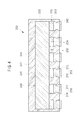
- FIGS. 1A and 1B depict a semiconductor package 100 constructed in accordance with a first embodiment of the present invention.
- the semiconductor package 100 comprises a generally quadrangular die attach pad or die pad 110 which defines a generally planar first (top) surface 111 and an opposed, generally planar second (bottom) surface 112 .
- Extending between the first and second surfaces 111 , 112 is a third (side) surface 113 .
- the third surface 113 does not extend perpendicularly between the first and second surfaces 111 , 112 .
- the third surface 113 extends at an incline or angle between the first and second surfaces 111 , 112 .
- the area of the first surface 111 is smaller than that of the second surface 112 .
- the die pad 110 may be formed from any one of a number of suitable conductive metal materials, including copper or an equivalent material, though the present invention is not intended to be limited to any specific material for the die pad 110 .
- the die pad 110 is preferably formed of a conductive metal material, such die pad 110 may be used to transfer an electrical signal from a semiconductor die (e.g., a ground signal or a power signal) to the exterior of the semiconductor package 100 , and may further be used to emit heat generated from the semiconductor die of the semiconductor package 100 .
- a semiconductor die e.g., a ground signal or a power signal
- first plated layer 114 which is of a predetermined thickness.
- the first plated layer 114 is sized so as to protrude beyond the circumference or periphery of the first surface 111 by a predetermined length or distance in a horizontal direction as viewed from the perspective shown in FIG. 1A .
- the area of each of the opposed top and bottom surfaces of the first plated layer 114 is at least equal and preferably larger than that of the first surface 111 of the die pad 110 .
- the protrusion of the first plated layer 114 beyond the peripheral edge of the first surface 111 is used to provide increased bonding power (i.e., a firmer mechanical interlock) between the die pad 110 and a package body of the semiconductor package 100 .
- the first plated layer 114 also provides an optimal bonding surface for one or more conductive wires extending from the semiconductor die of the semiconductor package 100 as will also be discussed in more detail below.
- the die pad 110 of the semiconductor package 100 includes a second plated layer 115 which is formed on the second surface 112 thereof in a predetermined thickness.
- the areas of the top and bottom surfaces of the second plated layer 115 are each substantially equal to that of the second surface 112 , i.e, the second plated layer 115 extends to, but does not protrude beyond, the periphery of the second surface 112 .
- an environment-friendly organic solderability preservation material hereinafter referred to as an “OSP” may be formed on the second surface 112 of the die pad 110 .
- the OSP functions to prevent oxidation of the die pad 110 until the semiconductor package 100 is mounted to an external device. Since the OSP is volatilized and removed during the high temperature mounting process typically used to facilitate the attachment of the semiconductor package 100 to an external device, such OSP would not disturb the process of mounting the die pad 110 of the semiconductor package 100 to the external device.
- the semiconductor package 100 comprises a conductive ring 120 which extends about or circumvents the die pad 110 , i.e., the die pad 110 resides in the open interior of the conductive ring 120 .
- the conductive ring 120 substantially functions as a ground ring or a power ring in the semiconductor package 100 .
- the conductive ring 120 defines a generally planar first (top) surface 121 , and an opposed, generally planar second (bottom) surface 122 . Extending between the first and second surfaces 121 , 122 is a third (side) surface 123 . As best seen in FIG. 1A , the third surface 123 does not extend perpendicularly between the first and second surfaces 121 , 122 .
- the third surface 123 extends at an incline or angle between the first and second surfaces 121 , 122 .
- the area of the first surface 121 is smaller than that of the second surface 122 .
- the conductive ring 120 may be formed from any one of a number of suitable conductive metal materials, including copper or an equivalent material, though the present invention is not intended to be limited to any specific material for the conductive ring 120 .
- the conductive ring 120 is preferably formed of a conductive metal material, such conductive ring 120 may be used to transfer an electrical signal from a semiconductor die (e.g., a ground signal or a power signal) to the exterior of the semiconductor package 100 , and may further be used to emit heat generated from the semiconductor die of the semiconductor package 100 .
- a semiconductor die e.g., a ground signal or a power signal
- first plated layer 124 formed on the first surface 111 of the conductive ring 120 is a first plated layer 124 which is of a predetermined thickness.
- the first plated layer 124 is sized so as to protrude beyond the inner and outer peripheral edges of the first surface 121 by a predetermined length or distance in a horizontal direction as viewed from the perspective shown in FIG. 1A .
- the area of each of the opposed top and bottom surfaces of the first plated layer 124 is at least equal and preferably larger than that of the first surface 121 of the conductive ring 120 .
- the protrusion of the first plated layer 124 beyond the inner and outer peripheral edges of the first surface 121 is used to provide increased bonding power (i.e., a firmer mechanical interlock) between the conductive ring 120 and a package body of the semiconductor package 100 .
- the first plated layer 124 also provides an optimal bonding surface for one or more conductive wires extending from the semiconductor die of the semiconductor package 100 as will also be discussed in more detail below.
- the conductive ring 120 of the semiconductor package 100 includes a second plated layer 125 which is formed on the second surface 122 thereof in a predetermined thickness.
- the areas of the top and bottom surfaces of the second plated layer 125 are each substantially equal to that of the second surface 122 , i.e, the second plated layer 125 extends to, but does not protrude beyond, the inner and outer peripheral edges of the second surface 122 .
- the above-described OSP may be formed on the second surface 122 of the conductive ring 120 .
- the OSP functions to prevent oxidation of the conductive ring 120 until the semiconductor package 100 is mounted to an external device. Since the OSP is volatilized and removed during the high temperature mounting process typically used to facilitate the attachment of the semiconductor package 100 to an external device, such OSP would not disturb the process of mounting the conductive ring 120 of the semiconductor package 100 to the external device.
- the semiconductor package 100 further comprises a plurality of I/O pads 130 which extend about or circumvent the conductive ring 120 . More particularly, as seen in FIG. 1B , the I/O pads 130 are segregated into a first inner set which at least partially circumvents the conductive ring 120 , and a second outer set which at least partially circumvents the inner set. Each of the I/O pads 130 defines a generally planar first (top) surface 131 , and an opposed, generally planar second (bottom) surface 132 . Extending between the first and second surfaces 131 , 132 is a third (side) surface 133 . As best seen in FIG.
- each of the I/O pads 130 may be formed from any one of a number of suitable conductive metal materials, including copper or an equivalent material, though the present invention is not intended to be limited to any specific material for the I/O pads 130 .
- each of the I/O pads 130 is preferably formed of a conductive metal material, such I/O pads 130 may be used to transfer an electrical signal from a semiconductor die (e.g., a ground signal or a power signal) to the exterior of the semiconductor package 100 , and may further be used to emit heat generated from the semiconductor die of the semiconductor package 100 .
- a semiconductor die e.g., a ground signal or a power signal
- first plated layer 134 formed on the first surface 131 of each of the I/O pads 130 is a first plated layer 134 which is of a predetermined thickness.
- the first plated layer 134 is sized so as to protrude beyond the periphery of the first surface 131 by a predetermined length or distance in a horizontal direction as viewed from the perspective shown in FIG. 1A .
- the area of each of the opposed top and bottom surfaces of each of the first plated layers 134 is at least equal and preferably larger than that of the first surface 131 of the corresponding I/O pad 130 to which it is applied.
- the protrusion of the first plated layer 134 beyond the peripheral edge of the first surface 131 is used to provide increased bonding power (i.e., a firmer mechanical interlock) between the corresponding I/O pad 130 and a package body of the semiconductor package 100 .
- the first plated layer 134 also provides an optimal bonding surface for one or more conductive wires extending from the semiconductor die of the semiconductor package 100 as will also be discussed in more detail below.
- each of the I/O pads 130 of the semiconductor package 100 includes a second plated layer 135 which is formed on the second surface 132 thereof in a predetermined thickness.
- the areas of the top and bottom surfaces of the second plated layer 135 are each substantially equal to that of the second surface 132 , i.e., the second plated layer 135 extends to, but does not protrude beyond, the peripheral edge of the corresponding second surface 132 .
- the above-described OSP may be formed on the second surface 132 of each of the I/O pads 130 .
- the OSP functions to prevent oxidation of the corresponding I/O pad 130 until the semiconductor package 100 is mounted to an external device. Since the OSP is volatilized and removed during the high temperature mounting process typically used to facilitate the attachment of the semiconductor package 100 to an external device, such OSP would not disturb the process of mounting the I/O pad 130 of the semiconductor package 100 to which it is applied to the external device.
- the number and arrangement of the I/O pads 130 as shown in FIGS. 1A and 1B is exemplary only, and that I/O pads 130 provided in differing numbers or arrangements are contemplated to be within the spirit and scope of the present invention.
- the I/O pads 130 may be arranged as a single set which at least partially circumvents the conductive ring 120 , or as inner, middle and outer sets which are concentrically arranged about the conductive ring 120 .
- the semiconductor package 100 of the present invention further comprises a semiconductor die 140 which is attached to the top surface of the first plating layer 114 applied to the die pad 110 .
- the semiconductor die 140 defines a generally planar first (top) surface 141 , and an opposed, generally planar second (bottom) surface 142 . Extending generally perpendicularly between the first and second surfaces 141 , 142 is a third (side) surface 143 . Formed on the first surface 141 in close proximity to the peripheral edge thereof is a plurality of bonding pads 144 of the semiconductor die 140 .
- the semiconductor die 140 is adhered to the first plated layer 114 formed on the die pad 110 through the use of an adhesive layer 150 .
- the adhesive layer 150 may comprise a general liquid epoxy adhesive, a both-side adhesive tape, or any other suitable equivalent material, the present invention not being limited to any particular material for the adhesive layer 150 .
- the width of the semiconductor die 140 is preferably smaller than that of the die pad 110 , and in particular the first plated layer 114 formed thereon, for purposes which will be described in more detail below.
- At least one first conductive wire 160 is used to electrically connect the semiconductor die 140 to the die pad 110 . More particularly, a first conductive wire 160 extends between a respective one of the bonding pads 144 of the semiconductor die 140 and the top surface of the first plated layer 114 formed on the die pad 110 . Importantly, the reduced width of the semiconductor die 140 in comparison to that of the first plated layer 114 provides sufficient space to accommodate that end of the first conductive wire 160 which is extended and bonded to the first plated layer 114 . The first conductive wire(s) 160 may be used to cause the ground signal of the semiconductor die 140 to be transferred to the die pad 110 .
- the first conductive wire(s) 160 may be used to cause the power signal from an external source to be transferred to the semiconductor die 140 through the die pad 110 .
- the first conductive wire(s) 160 may comprise a gold wire, an aluminum wire, a copper wire, or an equivalent material, the present invention not being limited to any specific material for the conductive wire(s) 160 .
- the semiconductor package 100 includes at least one second conductive wire 170 which is used to electrically connect the semiconductor die 140 to the conductive ring 120 . More particularly, the second conductive wire 170 extends between and electrically connects a respective one of the bonding pads 144 of the semiconductor die 140 to the first plated layer 124 formed on the conductive ring 120 .
- the second conductive wire(s) 170 may be used to cause the ground signal of the semiconductor die 140 to be transferred to the conductive ring 120 .
- the second conductive wire(s) 170 may also be used to cause the power signal from an external source to be transferred to the semiconductor die 140 through the conductive ring 120 .
- the second conductive wire(s) 170 may be fabricated from any one of the materials described above in relation to the first conductive wire(s) 160 .
- the semiconductor package 100 further comprises at least one third conductive wire 180 which is used to electrically connect the semiconductor die 140 to at least one of the I/O pads 130 .
- the semiconductor package 100 will include a plurality of conductive wires 180 which are used to electrically connect each of the I/O pads 130 included in the semiconductor package 100 to respective ones of the bonding pads 144 of the semiconductor die 140 . More particularly, as is further seen in FIG. 1A , each of the conductive wires 180 extends between one of the bonding pads 144 and the first plated layer 134 formed on a respective one of the I/O pads 130 .
- the third conductive wires 180 may be used to cause the control signals or the communication signals of the semiconductor die 140 to be transferred to each of the I/O pads 130 .
- the third conductive wires 180 may also be used to cause the control signal or the communication signal from an external source to be transferred to the semiconductor die 140 through one or more of the I/O pads 130 .
- the third conductive wires 180 are also each preferably fabricated from one of the above-described materials used in relation to the conductive wires 160 , 170 .
- portions of the die pad 110 , conductive ring 120 , I/O pads 130 , first plated layers 114 , 124 , 134 , conductive wires 160 , 170 , 180 , and semiconductor die 140 are covered by an encapsulant material which hardens into a package body 190 of the semiconductor package 100 .
- the package body 190 defines a generally planar first (top) surface 191 , and an opposed, generally planar second (bottom) surface 192 . Extending generally perpendicularly between the first and second surfaces 191 , 192 is a third (side) surface 193 . As is best seen in FIG.
- the second plated layer 115 (or OSP) formed on the die pad 110 , the second plated layer 125 (or OSP) formed on the conductive ring 120 , and the second plated layer 135 (or OSP) formed on each of the I/O pads 130 will be exposed in and protrude outwardly from the second surface 192 of the package body 130 .
- the die pad 110 , the conductive ring 120 , and each of the I/O pads 130 may be easily mounted to an external device.
- each of the second surfaces 112 , 122 , 132 will be exposed in and extend in substantially flush relation to the second surface 192 of the package body 190 .
- the encapsulant material used to form the package body 190 also underfills those portions of the first plated layers 114 , 124 , 134 which overhang corresponding ones of the first surfaces 111 , 121 , 131 . As indicated above, such underfill assists in providing a firm mechanical interlock between the package body 190 and the die pad 110 , conductive ring 120 and I/O pads 130 . It is contemplated that the encapsulant used to form the package body 190 may comprise an epoxy compound that performs the encapsulation through a molding process, a liquid encapsulant that performs the encapsulation through a dispenser, or equivalent materials thereto, the present invention not being limited to any specific material for the encapsulant.
- the die pad 110 is generally used to transfer the ground signal or the power signal of the semiconductor die 140 inside or outside the semiconductor package 100 , and is further used to emit heat generated by the semiconductor die 140 to the outside of the semiconductor package 100 .
- the conductive ring 120 is generally used to transfer the ground signal or the power signal of the semiconductor die 140 inside or outside the semiconductor package 100 .
- the I/O pads 130 are generally used to transfer the control signal or the communication of the semiconductor die 140 inside or outside the semiconductor package 100 .
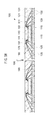
- FIG. 2A depicts one of the I/O pads 130 of the semiconductor package 100 , including the first and second plated layers 134 , 135 formed thereon.
- the first plated layer 134 of each I/O pad 130 may comprise electrolytic Ag, direct immersion Au, and suitable equivalent materials.
- the first plated layer 134 may be substituted with a variant first plated layer 134 a which may comprise adjacent layers of electrolytic Ni and electrolytic Au, adjacent layers of electroless Ni and electroless Au, adjacent layers of electroless Ni and immersion Au, adjacent layers of electroless Ni and autocatalysis Au, and suitable equivalent materials. As shown in FIG.
- the first plated layer 134 may also be substituted with a variant first plated layer 134 b which may comprise three adjacent layers of electroless Ni, electroless Pd and immersion Au, and suitable equivalent materials.
- the above-described first plated layers 134 , 134 a , 134 b may be varied according to the size of the semiconductor package 100 , the price of the semiconductor package 100 , the kind of conductive wire(s) 180 used in the semiconductor package 100 , the kind of encapsulant used to form the package body 190 , and a plurality of other variables.
- the size of material used in relation to the first plated layers 134 , 134 a , 134 b is not intended to be limited in the present invention.
- FIG. 3A depicts one of the I/O pads 130 of the semiconductor package 100 , including the first and second plated layers 134 , 135 formed thereon.
- the second plated layer 135 of each I/O pad 130 may comprise immersion Sn, direct immersion Au, OSP, and suitable equivalent materials.
- the second plated layer 135 may be substituted with a variant second plated layer 135 a which may comprise adjacent layers of electroless Ni and electroless Au, and suitable equivalent materials. As shown in FIG.
- the second plated layer 135 may also be substituted with a variant second plated layer 135 b which may comprise three adjacent layers of electroless Ni, electroless Pd and immersion Au, adjacent layers of electroless Ni and immersion Au, adjacent layers of electroless Ni and autocatalysis Au, and suitable equivalent materials.
- the above-described second plated layers 135 , 135 a , 135 b may be varied according to the size of the semiconductor package 100 , the price of the semiconductor package 100 , the mounting environment for the semiconductor package 100 , and a plurality of other variables.
- the size of material used in relation to the first plated layers 135 , 135 a , 135 b is not intended to be limited in the present invention.
- the semiconductor package 200 comprises a plurality of I/O pads 210 .
- Each of the I/O pads 210 defines a generally planar first (top) surface 211 , and an opposed, generally planar second (bottom) surface 212 .
- Extending between the first and second surfaces 131 , 132 is a third (side) surface 213 .
- the third surface 213 does not extend perpendicularly between the first and second surfaces 211 , 212 . Rather, the third surface 213 extends at an incline or angle between the first and second surfaces 211 , 212 .
- each of the I/O pads 210 may be formed from any one of a number of suitable conductive metal materials, including copper or an equivalent material, though the present invention is not intended to be limited to any specific material for the I/O pads 210 .
- each of the I/O pads 210 is preferably formed of a conductive metal material, such I/O pads 210 may be used to transfer an electrical signal from a semiconductor die (e.g., a ground signal or a power signal) to the exterior of the semiconductor package 200 , and may further be used to emit heat generated from the semiconductor die of the semiconductor package 200 .
- first plated layer 214 formed on the first surface 211 of each of the I/O pads 210 is a first plated layer 214 which is of a predetermined thickness.
- the first plated layer 214 is sized so as to protrude beyond the periphery of the first surface 211 by a predetermined length or distance in a horizontal direction as viewed from the perspective shown in FIG. 4 .
- the area of each of the opposed top and bottom surfaces of each of the first plated layers 214 is at least equal and preferably larger than that of the first surface 211 of the corresponding I/O pad 210 to which it is applied.
- the protrusion of the first plated layer 214 beyond the peripheral edge of the first surface 211 is used to provide increased bonding power (i.e., a firmer mechanical interlock) between the corresponding I/O pad 210 and a package body of the semiconductor package 200 .
- each of the I/O pads 210 of the semiconductor package 200 includes a second plated layer 215 which is formed on the second surface 212 thereof in a predetermined thickness.
- the areas of the top and bottom surfaces of the second plated layer 215 are each substantially equal to that of the second surface 212 , i.e., the second plated layer 215 extends to, but does not protrude beyond, the peripheral edge of the corresponding second surface 212 .
- the above-described OSP may be formed on the second surface 212 of each of the I/O pads 210 .
- the OSP functions to prevent oxidation of the corresponding I/O pad 210 until the semiconductor package 200 is mounted to an external device. Since the OSP is volatilized and removed during the high temperature mounting process typically used to facilitate the attachment of the semiconductor package 200 to an external device, such OSP would not disturb the process of mounting the I/O pad 210 of the semiconductor package 200 to which it is applied to the external device. Those of ordinary skill in the art will recognize that the I/O pads 210 of the semiconductor package 200 may be provided in any number and arrangement without departing from the spirit and scope of the present invention.
- the semiconductor package 200 of the present invention further comprises a semiconductor die 230 .
- the semiconductor die 230 defines a generally planar first (top) surface 231 , and an opposed, generally planar second (bottom) surface 232 . Extending generally perpendicularly between the first and second surfaces 231 , 232 is a third (side) surface 233 .
- Formed on the second surface 232 is a plurality of bonding pads 234 of the semiconductor die 230 .
- each of the bonding pads 234 is electrically connected to the first plated layer 214 of a respective one of the I/O pads 210 .
- Such electrical connection is preferably facilitated by a conductive bump 220 which is interposed between each of the bonding pads 234 and respective ones of the first plated layers 214 in the manner shown in FIG. 4 . More particularly, each conductive bump 220 is melted so as to effectively join and thus electrically connect each first plated layer 214 to a corresponding one of the bonding pads 234 . As such, the conductive bumps 220 function to electrically connect the semiconductor die 230 to the I/O pads 210 in an arrangement commonly referred to as flip chip type connection.
- Each conductive bump 220 may comprise gold, silver, solder, leadless solder, anisotropic conductive film, and suitable equivalent materials, the present invention not being limited to any particular material for the conductive bumps 220 .
- the package body 240 defines a generally planar first (top) surface 241 , and an opposed, generally planar second (bottom) surface 242 . Extending generally perpendicularly between the first and second surfaces 241 , 242 is a third (side) surface 243 . As is best seen in FIG.
- the second plated layer 215 (or OSP) formed on each of the I/O pads 210 will be exposed in and protrude outwardly from the second surface 242 of the package body 240 .
- each of the I/O pads 210 may be easily mounted to an external device.
- the second plated layers 215 or the OSP's are not formed on respective ones of the I/O pads 210 , each of the second surfaces 212 will be exposed in and extend in substantially flush relation to the second surface 242 of the package body 240 .
- the encapsulant material used to form the package body 240 also underfills those portions of the first plated layers 214 which overhang corresponding ones of the first surfaces 211 . As indicated above, such underfill assists in providing a firm mechanical interlock between the package body 240 and the I/O pads 210 . It is contemplated that the encapsulant used to form the package body 240 may comprise an epoxy compound that performs the encapsulation through a molding process, a liquid encapsulant that performs the encapsulation through a dispenser, or equivalent materials thereto, the present invention not being limited to any specific material for the encapsulant.
- FIGS. 5A-5M there is shown an exemplary sequence of steps which may be used to facilitate the fabrication of multiple semiconductor packages 100 .
- the fabrication process described below in relation to FIGS. 5A-5M is depicted as being implemented in relation to the simultaneous fabrication of two semiconductor packages 100 , those of ordinary skill in the art will recognize that such process is also applicable to the fabrication of a single semiconductor package 100 , or to the simultaneous fabrication of more than two semiconductor packages 100 without departing from the spirit and scope of the present invention.
- a carrier 101 is prepared.
- the carrier 101 is preferably fabricated from a material which is capable of maintaining a predetermined stiffness so as not to be susceptible to warpage during the process of fabricating the semiconductor packages 100 .
- the carrier 101 is further preferably fabricated from a material which is capable of being removed by an etching liquid or etchant during the process of fabricating the semiconductor packages 100 .
- the carrier 101 will be formed of a metal such as, for example, copper or a suitable equivalent material.
- the present invention is not intended to be limited to any particular material for the carrier 101 .
- a barrier layer 102 is formed on the top surface of the carrier 101 . It is contemplated that the barrier layer 102 will be fabricated from a material which is resistant to being etched by etching liquids which are adapted to etch other components such as the copper carrier 101 during the process of fabricating the semiconductor packages 100 .
- the barrier layer 102 may be formed of, for example, nickel or a suitable equivalent material. In this regard, nickel is a suitable material for the barrier layer 102 since it does not react with an etching liquid which is otherwise suitable to etch copper. However, the present invention is not intended to be limited to any particular material for use in relation to the barrier layer 102 .
- the barrier layer 102 may be formed by plating nickel having a predetermined thickness on the top surface of the carrier 101 as shown in FIG. 5B .
- a pad layer 103 is formed on the barrier layer 102 .
- the pad layer 103 is eventually etched in a manner facilitating the formation of the die pad 110 , the conductive ring 120 , and the I/O pads 130 of each semiconductor package 100 .
- the pad layer 103 will be fabricated from a material having excellent electrical conductivity and thermal conductivity.
- copper or a suitable equivalent material may be used as the material for forming the pad layer 103 .
- the present invention is not intended to be limited to be any specific material for the pad layer 103 .
- the pad layer 103 may be formed by plating copper having a predetermined thickness on the barrier layer 102 in the manner shown in FIG. 5C .
- a first dry film 104 is applied to the pad layer 103 , with a second dry film 105 being applied to the bottom surface of the carrier 101 , i.e., that surface of the carrier 101 opposite that having the barrier layer 102 applied thereto.
- the second dry film 105 is substantially continuous, and covers the entirety of the bottom surface of the carrier 101 .
- the first dry film 104 applied to the pad layer 103 is exposed and developed in a manner forming a predetermined pattern. Such pattern is one which will ultimately define the die pads 110 , conductive rings 120 and I/O pads 130 of multiple semiconductor packages 100 .
- the first plated layers 114 , 124 , 134 are formed by applying any of the suitable materials described above in relation to FIGS. 2A-2C onto those portions of the exposed surface of the pad layer 103 which are not covered by the patterned first dry film 104 .
- the first dry film 104 is removed, thus facilitating formation of spaces or voids between the fully formed first plated layers 114 , 124 , 134 in the manner shown FIG. 5E .
- an etching process is performed by using the first plated layers 114 , 124 , 134 as a mask such that the die pad 110 , the conductive ring 120 , and the I/O pads 130 of each of the semiconductor packages 100 are formed and separated from each other.
- the etching liquid used in the etching process shown in FIG. 5F is preferably one which will not react with the first plated layers 114 , 124 , 134 , or the barrier layer 102 .
- the etching liquid reacts only with the material used to form the pad layer 103 .
- the barrier layer 102 is effectively exposed between the resultant die pads 110 , conductive rings 120 and I/O pads 130 . Additionally, in the etching process, it is contemplated that each of the die pads 110 , conductive rings 120 and I/O pads 130 will be slightly over etched by the etching liquid, thereby forming the above-described inclined third surfaces 113 , 123 , 133 thereon and further resulting in the first plated layers 114 , 124 , 134 horizontally protruding therefrom in the manner facilitating the creation of the above-described overhang structure. Upon the completion of the etching of the pad layer 103 , the second dry film 105 is removed from the bottom surface of the carrier 101 .
- a semiconductor die 140 is attached to each of the die pads 110 formed as a result of the etching of the pad layer 103 in the manner described above in relation to FIG. 5F .
- each of the semiconductor dies 104 is attached to the first plated layer 114 formed on a respective one of the die pads 110 through the use of an adhesive layer 150 .
- the attachment of the semiconductor dies 140 to respective ones of the die pads 110 may be implemented through the use of a die bonder.
- each semiconductor die 140 is electrically connected to the die pad 110 , the conductive ring 120 and the I/O pads 130 of the corresponding semiconductor package 100 through the use of the above-described first, second and third conductive wires 160 , 170 , 180 .
- the first conductive wires 160 are extended from respective ones of the bonding pads 144 of the semiconductor die 140 to the first plated layer 114 formed on the corresponding die pad 110 .
- the second conductive wires 170 are extended from respective ones of the bonding pads 144 of the semiconductor die 140 to the first plated layer 124 formed on the corresponding conductive ring 120 .
- the conductive wires 180 are extended from respective ones of the bonding pads 144 of the semiconductor die 140 to the first plated layers 134 formed on corresponding ones of the I/O pads 130 .
- the bonding of the bond wires 160 , 170 , 180 in the above-described manner may be implemented through the use of a wire bonder.
- the package bodies 190 of the semiconductor packages 100 are formed by applying a layer of encapsulant material over the semiconductor dies 140 , the conductive wires 160 , 170 , 180 , the first plated layers 114 , 124 , 134 , the die pads 110 , the conductive rings 120 , and the I/O pads 130 .
- encapsulant material also flows into direct contact with those portions of the barrier layer 102 exposed as a result of the etching of the pad layer 103 to form the die pads 110 , conductive rings 120 and I/O pads 130 .
- the carrier 101 is removed.
- the removal of the carrier 101 is preferably facilitated by an etching process through the use of a suitable etching liquid. Since the etching liquid preferably used to etch the carrier 101 does not react with the barrier layer 102 , the barrier layer 102 is exposed upon the removal of the carrier 101 .
- the barrier layer 102 is etched and completely removed through the use of a suitable etching liquid.
- the barrier layer 102 may only be partially removed.
- the etching liquid used to etch the barrier layer 102 is one which does not react with the previously formed die pads 110 , conductive pads 120 and I/O pads 130 .
- the etching liquid is also one which does not react with the encapsulant material used to form the integrally connected package bodies 190 .
- the second surfaces 112 , 122 , 132 of the die pads 110 , conductive rings 120 and I/O pads 130 are exposed in the bottom surfaces of respective ones of the integrally connected package bodies 190 formed from the hardened encapsulant material in the manner shown in FIG. 5K .
- the second plated layers 115 , 125 , 135 are formed on the second surfaces 112 , 122 , 132 of respective ones of the die pads 110 , conductive rings 120 and I/O pads 130 .
- the second plated layers 115 , 125 , 135 are formed by applying any of the suitable materials described above in relation to FIGS. 3A-3C onto the second surfaces 112 , 122 , 132 of respective ones of the die pads 110 , conductive rings 120 and I/O pads 130 .
- the fully formed second plated layers 115 , 125 , 135 typically protrude downwardly from the bottom surfaces 192 of the integrally connected package bodies 190 formed by the hardened encapsulant material.
- the step of forming the second plated layers 115 , 125 , 135 as shown in FIG. 5L may be substituted with the formation of the above-described OSP's on the second surface 112 of each die pad 110 , the second surface 122 of each conductive ring 120 , and the second surface 132 of each I/O pad 130 .
- a singulation process is conducted to separate the fully formed semiconductor packages 100 from each other.
- the hardened encapsulant material is sawed in a manner forming the separate package bodies 190 of the semiconductor packages 100 .
- the sawing process may be completed through the use of, for example, a sawing tool 106 . Any surface of each package body 190 may be marking-processed by laser or ink before the performance of the singulation process.
- the barrier layer 102 may be partially removed through the completion of a suitable etching process as opposed to being completely removed.
- a dry film 104 may be applied to the exposed surface of the barrier layer 102 , with the dry film 104 thereafter being patterned in the manner shown in FIG. 6A .
- the dry film 104 partially remains on the bottom surface of the barrier layer 102 , and covers areas corresponding to the second surface 112 of each of the die pads 110 , the second surface 122 of each of the conductive rings 120 , and the second surface 132 of each of the I/O pads 130 . As shown in FIG.
- FIGS. 6A and 6B subsequent to the patterning of the dry film 104 , an etching process is completed, with the remaining dry film 104 functioning as a mask in a manner allowing for the etching of the barrier layer 102 in a manner forming the second plated layers 115 , 125 , 135 .
- the fabrication steps shown in FIGS. 6A and 6B may be implemented as an alternative to the fabrication steps shown and described above in relation to FIGS. 5K and 5L .
- FIGS. 7A-7M there is shown an exemplary sequence of steps which may be used to facilitate the fabrication of multiple semiconductor packages 200 .
- the fabrication process described below in relation to FIGS. 7A-7M is depicted as being implemented in relation to the simultaneous fabrication of two semiconductor packages 200 , those of ordinary skill in the art will recognize that such process is also applicable to the fabrication of a single semiconductor package 200 , or to the simultaneous fabrication of more than two semiconductor packages 200 without departing from the spirit and scope of the present invention.
- a carrier 201 is prepared.
- the carrier 201 is preferably fabricated from a material which is capable of maintaining a predetermined stiffness so as not to be susceptible to warpage during the process of fabricating the semiconductor packages 200 .
- the carrier 201 is further preferably fabricated from a material which is capable of being removed by an etching liquid or etchant during the process of fabricating the semiconductor packages 200 .
- the carrier 201 will be formed of a metal such as, for example, copper or a suitable equivalent material.
- the present invention is not intended to be limited to any particular material for the carrier 201 .
- a barrier layer 202 is formed on the top surface of the carrier 201 .
- the barrier layer 202 will be fabricated from a material which is resistant to being etched by etching liquids which are adapted to etch other components such as the copper carrier 201 during the process of fabricating the semiconductor packages 200 .
- the barrier layer 202 may be formed of, for example, nickel or a suitable equivalent material.
- nickel is a suitable material for the barrier layer 202 since it does not react with an etching liquid which is otherwise suitable to etch copper.
- the present invention is not intended to be limited to any particular material for use in relation to the barrier layer 202 .
- the barrier layer 202 may be formed by plating nickel having a predetermined thickness on the top surface of the carrier 201 as shown in FIG. 7B .
- a pad layer 203 is formed on the barrier layer 202 .
- the pad layer 103 is eventually etched in a manner facilitating the formation of the I/O pads 210 of each semiconductor package 200 .
- the pad layer 203 will be fabricated from a material having excellent electrical conductivity and thermal conductivity.
- copper or a suitable equivalent material may be used as the material for forming the pad layer 203 .
- the present invention is not intended to be limited to be any specific material for the pad layer 203 .
- the pad layer 203 may be formed by plating copper having a predetermined thickness on the barrier layer 202 in the manner shown in FIG. 7C .
- a first dry film 204 is applied to the pad layer 203 , with a second dry film 205 being applied to the bottom surface of the carrier 201 , i.e., that surface of the carrier 201 opposite that having the barrier layer 202 applied thereto.
- the second dry film 205 is substantially continuous, and covers the entirety of the bottom surface of the carrier 201 .
- the first dry film 204 applied to the pad layer 203 is exposed and developed in a manner forming a predetermined pattern. Such pattern is one which will ultimately define the I/O pads 210 of multiple semiconductor packages 200 .
- the first plated layers 214 are formed by applying any of the suitable materials described above in relation to FIGS. 2A-2C onto those portions of the exposed surface of the pad layer 203 which are not covered by the patterned first dry film 204 .
- the first dry film 204 is removed, thus facilitating formation of spaces or voids between the fully formed first plated layers 214 in the manner shown FIG. 7E .
- an etching process is performed by using the first plated layers 214 as a mask such that the I/O pads 210 of each of the semiconductor packages 200 are formed and separated from each other.
- the etching liquid used in the etching process shown in FIG. 7F is preferably one which will not react with the first plated layers 214 , or the barrier layer 202 .
- the etching liquid reacts only with the material used to form the pad layer 203 .
- the barrier layer 202 is effectively exposed between the resultant I/O pads 210 .
- each of the I/O pads 210 will be slightly over etched by the etching liquid, thereby forming the above-described inclined third surfaces 213 thereon and further resulting in the first plated layers 214 horizontally protruding therefrom in the manner facilitating the creation of the above-described overhang structure.
- the second dry film 205 is removed from the bottom surface of the carrier 201 .
- a semiconductor die 230 is attached and electrically connected to each of the I/O pads 210 of the corresponding semiconductor package 200 , such I/O pads 210 being formed as a result of the etching of the pad layer 203 in the manner described above in relation to FIG. 7F .
- Each of the bonding pads 234 of each semiconductor die 230 includes a conductive bump 220 formed thereon. Each conductive bump 220 is brought into direct contact with the first plated layer 214 of a respective one of the I/O pads 210 of the corresponding semiconductor package 200 .
- each conductive bump 220 is melted so as to effectively join and thus electrically connect each first plated layer 214 to a respective one of the bonding pads 234 of the corresponding semiconductor die 230 .
- the reflow process is typically conducted at temperatures in the range of from about 150° C. to about 250° C.
- the conductive bumps 220 function to electrically connect each semiconductor die 230 to the I/O pads 210 of the corresponding semiconductor package 200 in an arrangement commonly referred to as flip chip type connection.
- the package bodies 240 of the semiconductor packages 200 are formed by applying a layer of encapsulant material over the semiconductor dies 230 , the first plated layers 214 , the reflowed conductive bumps 220 , and the I/O pads 210 .
- encapsulant material also flows into direct contact with those portions of the barrier layer 202 exposed as a result of the etching of the pad layer 203 to form the I/O pads 210 .
- the carrier 201 is removed.
- the removal of the carrier 201 is preferably facilitated by an etching process through the use of a suitable etching liquid. Since the etching liquid preferably used to etch the carrier 201 does not react with the barrier layer 202 , the barrier layer 202 is exposed upon the removal of the carrier 201 .
- the barrier layer 202 is etched and completely removed through the use of a suitable etching liquid.
- the barrier layer 202 may only be partially removed.
- the etching liquid used to etch the barrier layer 202 is one which does not react with the previously formed I/O pads 210 .
- the etching liquid is also one which does not react with the encapsulant material used to form the integrally connected package bodies 240 .
- the second surfaces 212 of the I/O pads 210 are exposed in the bottom surfaces of respective ones of the integrally connected package bodies 240 formed from the hardened encapsulant material in the manner shown in FIG. 7K .
- the second plated layers 215 are formed on the second surfaces 212 of respective ones of the I/O pads 210 .
- the second plated layers 215 are formed by applying any of the suitable materials described above in relation to FIGS. 3A-3C onto the second surfaces 212 of respective ones of the I/O pads 210 .
- the fully formed second plated layers 215 typically protrude downwardly from the bottom surfaces 242 of the integrally connected package bodies 240 formed by the hardened encapsulant material.
- the step of forming the second plated layers 215 as shown in FIG. 7L may be substituted with the formation of the above-described OSP's on the second surface 212 of each I/O pad 210 .
- a singulation process is conducted to separate the fully formed semiconductor packages 200 from each other.
- the hardened encapsulant material is sawed in a manner forming the separate package bodies 240 of the semiconductor packages 200 .
- the sawing process may be completed through the use of, for example, a sawing tool 206 . Any surface of each package body 240 may be marking-processed by laser or ink before the performance of the singulation process.
- the barrier layer 202 may be partially removed through the completion of a suitable etching process as opposed to being completely removed.
- a dry film 204 may be applied to the exposed surface of the barrier layer 202 , with the dry film 204 thereafter being patterned in the manner shown in FIG. 8A .
- the dry film 204 partially remains on the bottom surface of the barrier layer 202 , and covers areas corresponding to the second surface 212 of each of the I/O pads 210 . As shown in FIG.
- FIGS. 8A and 8B subsequent to the patterning of the dry film 204 , an etching process is completed, with the remaining dry film 204 functioning as a mask in a manner allowing for the etching of the barrier layer 202 in a manner forming the second plated layers 215 .
- the fabrication steps shown in FIGS. 8A and 8B may be implemented as an alternative to the fabrication steps shown and described above in relation to FIGS. 7K and 7L .
Abstract
Description
Claims (21)
Priority Applications (2)
| Application Number | Priority Date | Filing Date | Title |
|---|---|---|---|
| US11/866,886 US8089159B1 (en) | 2007-10-03 | 2007-10-03 | Semiconductor package with increased I/O density and method of making the same |
| US13/290,451 US8227921B1 (en) | 2007-10-03 | 2011-11-07 | Semiconductor package with increased I/O density and method of making same |
Applications Claiming Priority (1)
| Application Number | Priority Date | Filing Date | Title |
|---|---|---|---|
| US11/866,886 US8089159B1 (en) | 2007-10-03 | 2007-10-03 | Semiconductor package with increased I/O density and method of making the same |
Related Child Applications (1)
| Application Number | Title | Priority Date | Filing Date |
|---|---|---|---|
| US13/290,451 Continuation US8227921B1 (en) | 2007-10-03 | 2011-11-07 | Semiconductor package with increased I/O density and method of making same |
Publications (1)
| Publication Number | Publication Date |
|---|---|
| US8089159B1 true US8089159B1 (en) | 2012-01-03 |
Family
ID=45374588
Family Applications (2)
| Application Number | Title | Priority Date | Filing Date |
|---|---|---|---|
| US11/866,886 Active 2029-09-26 US8089159B1 (en) | 2007-10-03 | 2007-10-03 | Semiconductor package with increased I/O density and method of making the same |
| US13/290,451 Active US8227921B1 (en) | 2007-10-03 | 2011-11-07 | Semiconductor package with increased I/O density and method of making same |
Family Applications After (1)
| Application Number | Title | Priority Date | Filing Date |
|---|---|---|---|
| US13/290,451 Active US8227921B1 (en) | 2007-10-03 | 2011-11-07 | Semiconductor package with increased I/O density and method of making same |
Country Status (1)
| Country | Link |
|---|---|
| US (2) | US8089159B1 (en) |
Cited By (15)
| Publication number | Priority date | Publication date | Assignee | Title |
|---|---|---|---|---|
| US20120067627A1 (en) * | 2010-09-21 | 2012-03-22 | Robert Bosch Gmbh | Circuit Carrier and Method for Producing a Circuit Carrier |
| JP2013145825A (en) * | 2012-01-16 | 2013-07-25 | Dainippon Printing Co Ltd | Lead frame for semiconductor device |
| US20130249095A1 (en) * | 2012-03-26 | 2013-09-26 | Skyworks Solutions, Inc. | Gallium arsenide devices with copper backside for direct die solder attach |
| US20130299980A1 (en) * | 2012-05-10 | 2013-11-14 | Utac Thai Limited | Protruding terminals with internal routing interconnections semiconductor device |
| US8698291B2 (en) | 2011-12-15 | 2014-04-15 | Freescale Semiconductor, Inc. | Packaged leadless semiconductor device |
| US8803302B2 (en) * | 2012-05-31 | 2014-08-12 | Freescale Semiconductor, Inc. | System, method and apparatus for leadless surface mounted semiconductor package |
| US20150041994A1 (en) * | 2013-08-07 | 2015-02-12 | Texas Instruments Incorporated | Semiconductor package having recessed solder terminals |
| JP2016127261A (en) * | 2014-12-27 | 2016-07-11 | 日立マクセル株式会社 | Substrate for semiconductor device, method of manufacturing substrate for semiconductor device, and semiconductor device |
| US9666508B2 (en) | 2014-06-13 | 2017-05-30 | Skyworks Solutions, Inc. | Gallium arsenide devices with copper backside for direct die solder attach |
| US20180012828A1 (en) * | 2016-07-05 | 2018-01-11 | Danfoss Silicon Power Gmbh | Lead frame and method of fabricating the same |
| US20180166368A1 (en) * | 2016-12-09 | 2018-06-14 | Sh Materials Co., Ltd. | Lead frame |
| US10128169B1 (en) * | 2017-05-12 | 2018-11-13 | Stmicroelectronics, Inc. | Package with backside protective layer during molding to prevent mold flashing failure |
| US20190348387A1 (en) * | 2013-03-14 | 2019-11-14 | UTAC Headquarters Pte. Ltd. | Semiconductor packages and methods of packaging semiconductor devices |
| US20210159155A1 (en) * | 2019-11-22 | 2021-05-27 | Advanced Semiconductor Engineering, Inc. | Lead frame, package structure and method for manufacturing the same |
| US11291146B2 (en) | 2014-03-07 | 2022-03-29 | Bridge Semiconductor Corp. | Leadframe substrate having modulator and crack inhibiting structure and flip chip assembly using the same |
Families Citing this family (2)
| Publication number | Priority date | Publication date | Assignee | Title |
|---|---|---|---|---|
| TWI463579B (en) * | 2012-09-10 | 2014-12-01 | 矽品精密工業股份有限公司 | Quad flat no lead (qfn) semiconductor package and method of forming same |
| JP6913993B2 (en) * | 2016-08-05 | 2021-08-04 | マクセルホールディングス株式会社 | Substrates for semiconductor devices, manufacturing methods for semiconductor devices |
Citations (317)
| Publication number | Priority date | Publication date | Assignee | Title |
|---|---|---|---|---|
| US2596993A (en) | 1949-01-13 | 1952-05-20 | United Shoe Machinery Corp | Method and mold for covering of eyelets by plastic injection |
| US3435815A (en) | 1966-07-15 | 1969-04-01 | Micro Tech Mfg Inc | Wafer dicer |
| US3734660A (en) | 1970-01-09 | 1973-05-22 | Tuthill Pump Co | Apparatus for fabricating a bearing device |
| US3838984A (en) | 1973-04-16 | 1974-10-01 | Sperry Rand Corp | Flexible carrier and interconnect for uncased ic chips |
| US4054238A (en) | 1976-03-23 | 1977-10-18 | Western Electric Company, Inc. | Method, apparatus and lead frame for assembling leads with terminals on a substrate |
| US4189342A (en) | 1971-10-07 | 1980-02-19 | U.S. Philips Corporation | Semiconductor device comprising projecting contact layers |
| US4258381A (en) | 1977-12-07 | 1981-03-24 | Steag, Kernergie Gmbh | Lead frame for a semiconductor device suitable for mass production |
| US4289922A (en) | 1979-09-04 | 1981-09-15 | Plessey Incorporated | Integrated circuit package and lead frame |
| US4301464A (en) | 1978-08-02 | 1981-11-17 | Hitachi, Ltd. | Lead frame and semiconductor device employing the same with improved arrangement of supporting leads for securing the semiconductor supporting member |
| US4332537A (en) | 1978-07-17 | 1982-06-01 | Dusan Slepcevic | Encapsulation mold with removable cavity plates |
| US4417266A (en) | 1981-08-14 | 1983-11-22 | Amp Incorporated | Power and ground plane structure for chip carrier |
| US4451224A (en) | 1982-03-25 | 1984-05-29 | General Electric Company | Mold device for making plastic articles from resin |
| US4530152A (en) | 1982-04-01 | 1985-07-23 | Compagnie Industrielle Des Telecommunications Cit-Alcatel | Method for encapsulating semiconductor components using temporary substrates |
| US4541003A (en) | 1978-12-27 | 1985-09-10 | Hitachi, Ltd. | Semiconductor device including an alpha-particle shield |
| US4646710A (en) | 1982-09-22 | 1987-03-03 | Crystal Systems, Inc. | Multi-wafer slicing with a fixed abrasive |
| US4707724A (en) | 1984-06-04 | 1987-11-17 | Hitachi, Ltd. | Semiconductor device and method of manufacturing thereof |
| US4727633A (en) | 1985-08-08 | 1988-03-01 | Tektronix, Inc. | Method of securing metallic members together |
| US4737839A (en) | 1984-03-19 | 1988-04-12 | Trilogy Computer Development Partners, Ltd. | Semiconductor chip mounting system |
| US4756080A (en) | 1986-01-27 | 1988-07-12 | American Microsystems, Inc. | Metal foil semiconductor interconnection method |
| US4812896A (en) | 1986-11-13 | 1989-03-14 | Olin Corporation | Metal electronic package sealed with thermoplastic having a grafted metal deactivator and antioxidant |
| US4862245A (en) | 1985-04-18 | 1989-08-29 | International Business Machines Corporation | Package semiconductor chip |
| US4862246A (en) | 1984-09-26 | 1989-08-29 | Hitachi, Ltd. | Semiconductor device lead frame with etched through holes |
| US4907067A (en) | 1988-05-11 | 1990-03-06 | Texas Instruments Incorporated | Thermally efficient power device package |
| US4920074A (en) | 1987-02-25 | 1990-04-24 | Hitachi, Ltd. | Surface mount plastic package semiconductor integrated circuit, manufacturing method thereof, as well as mounting method and mounted structure thereof |
| US4935803A (en) | 1988-09-09 | 1990-06-19 | Motorola, Inc. | Self-centering electrode for power devices |
| US4942454A (en) | 1987-08-05 | 1990-07-17 | Mitsubishi Denki Kabushiki Kaisha | Resin sealed semiconductor device |
| US4987475A (en) | 1988-02-29 | 1991-01-22 | Digital Equipment Corporation | Alignment of leads for ceramic integrated circuit packages |
| US5018003A (en) | 1988-10-20 | 1991-05-21 | Mitsubishi Denki Kabushiki Kaisha | Lead frame and semiconductor device |
| US5029386A (en) | 1990-09-17 | 1991-07-09 | Hewlett-Packard Company | Hierarchical tape automated bonding method |
| US5041902A (en) | 1989-12-14 | 1991-08-20 | Motorola, Inc. | Molded electronic package with compression structures |
| US5057900A (en) | 1988-10-17 | 1991-10-15 | Semiconductor Energy Laboratory Co., Ltd. | Electronic device and a manufacturing method for the same |
| US5059379A (en) | 1987-07-20 | 1991-10-22 | Mitsubishi Denki Kabushiki Kaisha | Method of resin sealing semiconductor devices |
| US5065223A (en) | 1989-05-31 | 1991-11-12 | Fujitsu Vlsi Limited | Packaged semiconductor device |
| US5070039A (en) | 1989-04-13 | 1991-12-03 | Texas Instruments Incorporated | Method of making an integrated circuit using a pre-served dam bar to reduce mold flash and to facilitate flash removal |
| US5087961A (en) | 1987-01-28 | 1992-02-11 | Lsi Logic Corporation | Semiconductor device package |
| US5091341A (en) | 1989-05-22 | 1992-02-25 | Kabushiki Kaisha Toshiba | Method of sealing semiconductor device with resin by pressing a lead frame to a heat sink using an upper mold pressure member |
| US5096852A (en) | 1988-06-02 | 1992-03-17 | Burr-Brown Corporation | Method of making plastic encapsulated multichip hybrid integrated circuits |
| US5118298A (en) | 1991-04-04 | 1992-06-02 | Advanced Interconnections Corporation | Through hole mounting of integrated circuit adapter leads |
| US5122860A (en) | 1987-08-26 | 1992-06-16 | Matsushita Electric Industrial Co., Ltd. | Integrated circuit device and manufacturing method thereof |
| US5134773A (en) | 1989-05-26 | 1992-08-04 | Gerard Lemaire | Method for making a credit card containing a microprocessor chip |
| US5151039A (en) | 1990-04-06 | 1992-09-29 | Advanced Interconnections Corporation | Integrated circuit adapter having gullwing-shaped leads |
| US5157480A (en) | 1991-02-06 | 1992-10-20 | Motorola, Inc. | Semiconductor device having dual electrical contact sites |
| US5157475A (en) | 1988-07-08 | 1992-10-20 | Oki Electric Industry Co., Ltd. | Semiconductor device having a particular conductive lead structure |
| US5168368A (en) | 1991-05-09 | 1992-12-01 | International Business Machines Corporation | Lead frame-chip package with improved configuration |
| US5172213A (en) | 1991-05-23 | 1992-12-15 | At&T Bell Laboratories | Molded circuit package having heat dissipating post |
| US5172214A (en) | 1991-02-06 | 1992-12-15 | Motorola, Inc. | Leadless semiconductor device and method for making the same |
| US5175060A (en) | 1989-07-01 | 1992-12-29 | Ibiden Co., Ltd. | Leadframe semiconductor-mounting substrate having a roughened adhesive conductor circuit substrate and method of producing the same |
| US5200362A (en) | 1989-09-06 | 1993-04-06 | Motorola, Inc. | Method of attaching conductive traces to an encapsulated semiconductor die using a removable transfer film |
| US5200809A (en) | 1991-09-27 | 1993-04-06 | Vlsi Technology, Inc. | Exposed die-attach heatsink package |
| US5214845A (en) | 1992-05-11 | 1993-06-01 | Micron Technology, Inc. | Method for producing high speed integrated circuits |
| US5216278A (en) | 1990-12-04 | 1993-06-01 | Motorola, Inc. | Semiconductor device having a pad array carrier package |
| US5218231A (en) | 1989-08-30 | 1993-06-08 | Kabushiki Kaisha Toshiba | Mold-type semiconductor device |
| US5221642A (en) | 1991-08-15 | 1993-06-22 | Staktek Corporation | Lead-on-chip integrated circuit fabrication method |
| US5250841A (en) | 1992-04-06 | 1993-10-05 | Motorola, Inc. | Semiconductor device with test-only leads |
| US5252853A (en) | 1991-09-19 | 1993-10-12 | Mitsubishi Denki Kabushiki Kaisha | Packaged semiconductor device having tab tape and particular power distribution lead structure |
| US5258094A (en) | 1991-09-18 | 1993-11-02 | Nec Corporation | Method for producing multilayer printed wiring boards |
| US5266834A (en) | 1989-03-13 | 1993-11-30 | Hitachi Ltd. | Semiconductor device and an electronic device with the semiconductor devices mounted thereon |
| US5278446A (en) | 1992-07-06 | 1994-01-11 | Motorola, Inc. | Reduced stress plastic package |
| US5277972A (en) | 1988-09-29 | 1994-01-11 | Tomoegawa Paper Co., Ltd. | Adhesive tapes |
| US5279029A (en) | 1990-08-01 | 1994-01-18 | Staktek Corporation | Ultra high density integrated circuit packages method |
| US5281849A (en) | 1991-05-07 | 1994-01-25 | Singh Deo Narendra N | Semiconductor package with segmented lead frame |
| US5285352A (en) | 1992-07-15 | 1994-02-08 | Motorola, Inc. | Pad array semiconductor device with thermal conductor and process for making the same |
| US5294897A (en) | 1992-07-20 | 1994-03-15 | Mitsubishi Denki Kabushiki Kaisha | Microwave IC package |
| US5327008A (en) | 1993-03-22 | 1994-07-05 | Motorola Inc. | Semiconductor device having universal low-stress die support and method for making the same |
| US5332864A (en) | 1991-12-27 | 1994-07-26 | Vlsi Technology, Inc. | Integrated circuit package having an interposer |
| US5336931A (en) | 1993-09-03 | 1994-08-09 | Motorola, Inc. | Anchoring method for flow formed integrated circuit covers |
| US5335771A (en) | 1990-09-25 | 1994-08-09 | R. H. Murphy Company, Inc. | Spacer trays for stacking storage trays with integrated circuits |
| US5343076A (en) | 1990-07-21 | 1994-08-30 | Mitsui Petrochemical Industries, Ltd. | Semiconductor device with an airtight space formed internally within a hollow package |
| US5358905A (en) | 1993-04-02 | 1994-10-25 | Texas Instruments Incorporated | Semiconductor device having die pad locking to substantially reduce package cracking |
| US5365106A (en) | 1992-10-27 | 1994-11-15 | Kabushiki Kaisha Toshiba | Resin mold semiconductor device |
| US5381042A (en) | 1992-03-31 | 1995-01-10 | Amkor Electronics, Inc. | Packaged integrated circuit including heat slug having an exposed surface |
| EP0393997B1 (en) | 1989-04-20 | 1995-02-01 | Honeywell Inc. | Method of providing a variable-pitch leadframe assembly |
| US5391439A (en) | 1990-09-27 | 1995-02-21 | Dai Nippon Printing Co., Ltd. | Leadframe adapted to support semiconductor elements |
| US5406124A (en) | 1992-12-04 | 1995-04-11 | Mitsui Toatsu Chemicals, Inc. | Insulating adhesive tape, and lead frame and semiconductor device employing the tape |
| US5410180A (en) | 1992-07-28 | 1995-04-25 | Shinko Electric Industries Co., Ltd. | Metal plane support for multi-layer lead frames and a process for manufacturing such frames |
| US5414299A (en) | 1993-09-24 | 1995-05-09 | Vlsi Technology, Inc. | Semi-conductor device interconnect package assembly for improved package performance |
| US5417905A (en) | 1989-05-26 | 1995-05-23 | Esec (Far East) Limited | Method of making a card having decorations on both faces |
| US5428248A (en) | 1992-08-21 | 1995-06-27 | Goldstar Electron Co., Ltd. | Resin molded semiconductor package |
| US5434057A (en) | 1994-02-02 | 1995-07-18 | Quidel Corporation | Sperm motility assay and devices |
| US5444301A (en) | 1993-06-23 | 1995-08-22 | Goldstar Electron Co. Ltd. | Semiconductor package and method for manufacturing the same |
| US5452511A (en) | 1993-11-04 | 1995-09-26 | Chang; Alexander H. C. | Composite lead frame manufacturing method |
| US5454905A (en) | 1994-08-09 | 1995-10-03 | National Semiconductor Corporation | Method for manufacturing fine pitch lead frame |
| US5467032A (en) | 1993-11-09 | 1995-11-14 | Samsung Electronics Co., Ltd. | Word line driver circuit for a semiconductor memory device |
| US5474958A (en) | 1993-05-04 | 1995-12-12 | Motorola, Inc. | Method for making semiconductor device having no die supporting surface |
| US5484274A (en) | 1992-11-24 | 1996-01-16 | Neu Dynamics Corp. | Encapsulation molding equipment |
| US5493151A (en) | 1993-07-15 | 1996-02-20 | Kabushiki Kaisha Toshiba | Semiconductor device, lead frame and method for manufacturing semiconductor devices |
| US5508556A (en) | 1994-09-02 | 1996-04-16 | Motorola, Inc. | Leaded semiconductor device having accessible power supply pad terminals |
| US5517056A (en) | 1993-09-30 | 1996-05-14 | Motorola, Inc. | Molded carrier ring leadframe having a particular resin injecting area design for gate removal and semiconductor device employing the same |
| US5521429A (en) | 1993-11-25 | 1996-05-28 | Sanyo Electric Co., Ltd. | Surface-mount flat package semiconductor device |
| US5528076A (en) | 1995-02-01 | 1996-06-18 | Motorola, Inc. | Leadframe having metal impregnated silicon carbide mounting area |
| US5534467A (en) | 1993-03-18 | 1996-07-09 | Lsi Logic Corporation | Semiconductor packages for high I/O semiconductor dies |
| US5539251A (en) | 1992-05-11 | 1996-07-23 | Micron Technology, Inc. | Tie bar over chip lead frame design |
| US5543657A (en) | 1994-10-07 | 1996-08-06 | International Business Machines Corporation | Single layer leadframe design with groundplane capability |
| US5544412A (en) | 1994-05-24 | 1996-08-13 | Motorola, Inc. | Method for coupling a power lead to a bond pad in an electronic module |
| US5545923A (en) | 1993-10-22 | 1996-08-13 | Lsi Logic Corporation | Semiconductor device assembly with minimized bond finger connections |
| US5581122A (en) | 1994-10-25 | 1996-12-03 | Industrial Technology Research Institute | Packaging assembly with consolidated common voltage connections for integrated circuits |
| US5592025A (en) | 1992-08-06 | 1997-01-07 | Motorola, Inc. | Pad array semiconductor device |
| US5592019A (en) | 1994-04-19 | 1997-01-07 | Mitsubishi Denki Kabushiki Kaisha | Semiconductor device and module |
| US5594274A (en) | 1993-07-01 | 1997-01-14 | Nec Corporation | Lead frame for use in a semiconductor device and method of manufacturing the semiconductor device using the same |
| US5595934A (en) | 1995-05-17 | 1997-01-21 | Samsung Electronics Co., Ltd. | Method for forming oxide protective film on bonding pads of semiconductor chips by UV/O3 treatment |
| US5604376A (en) | 1994-06-30 | 1997-02-18 | Digital Equipment Corporation | Paddleless molded plastic semiconductor chip package |
| US5608267A (en) | 1992-09-17 | 1997-03-04 | Olin Corporation | Molded plastic semiconductor package including heat spreader |
| US5608265A (en) | 1993-03-17 | 1997-03-04 | Hitachi, Ltd. | Encapsulated semiconductor device package having holes for electrically conductive material |
| US5625222A (en) | 1993-11-18 | 1997-04-29 | Fujitsu Limited | Semiconductor device in a resin package housed in a frame having high thermal conductivity |
| US5633528A (en) | 1994-05-25 | 1997-05-27 | Texas Instruments Incorporated | Lead frame structure for IC devices with strengthened encapsulation adhesion |
| US5637922A (en) | 1994-02-07 | 1997-06-10 | General Electric Company | Wireless radio frequency power semiconductor devices using high density interconnect |
| US5639990A (en) | 1992-06-05 | 1997-06-17 | Mitsui Toatsu Chemicals, Inc. | Solid printed substrate and electronic circuit package using the same |
| US5640047A (en) | 1995-09-25 | 1997-06-17 | Mitsui High-Tec, Inc. | Ball grid assembly type semiconductor device having a heat diffusion function and an electric and magnetic shielding function |
| US5641997A (en) | 1993-09-14 | 1997-06-24 | Kabushiki Kaisha Toshiba | Plastic-encapsulated semiconductor device |
| US5644169A (en) | 1993-03-04 | 1997-07-01 | Goldstar Electron Co., Ltd. | Mold and method for manufacturing a package for a semiconductor chip and the package manufactured thereby |
| US5643433A (en) | 1992-12-23 | 1997-07-01 | Shinko Electric Industries Co., Ltd. | Lead frame and method for manufacturing same |
| US5646831A (en) | 1995-12-28 | 1997-07-08 | Vlsi Technology, Inc. | Electrically enhanced power quad flat pack arrangement |
| US5650663A (en) | 1995-07-03 | 1997-07-22 | Olin Corporation | Electronic package with improved thermal properties |
| US5661088A (en) | 1996-01-11 | 1997-08-26 | Motorola, Inc. | Electronic component and method of packaging |
| US5665996A (en) | 1994-12-30 | 1997-09-09 | Siliconix Incorporated | Vertical power mosfet having thick metal layer to reduce distributed resistance |
| EP0794572A2 (en) | 1996-03-07 | 1997-09-10 | Matsushita Electronics Corporation | Electronic component, method for making the same, and lead frame and mold assembly for use therein |
| US5673479A (en) | 1993-12-20 | 1997-10-07 | Lsi Logic Corporation | Method for mounting a microelectronic circuit peripherally-leaded package including integral support member with spacer |
| US5683806A (en) | 1988-09-29 | 1997-11-04 | Tomoegawa Paper Co., Ltd. | Adhesive tapes |
| US5683943A (en) | 1994-06-14 | 1997-11-04 | Dai Nippon Printing Co., Ltd. | Process for etching a semiconductor lead frame |
| US5689135A (en) | 1995-12-19 | 1997-11-18 | Micron Technology, Inc. | Multi-chip device and method of fabrication employing leads over and under processes |
| US5696666A (en) | 1995-10-11 | 1997-12-09 | Motorola, Inc. | Low profile exposed die chip carrier package |
| US5701034A (en) | 1994-05-03 | 1997-12-23 | Amkor Electronics, Inc. | Packaged semiconductor die including heat sink with locking feature |
| US5703407A (en) | 1995-02-14 | 1997-12-30 | Kabushiki Kaisha Toshiba | Resin-sealed type semiconductor device |
| US5710064A (en) | 1994-08-16 | 1998-01-20 | Samsung Electronics Co., Ltd. | Method for manufacturing a semiconductor package |
| US5723899A (en) | 1994-08-30 | 1998-03-03 | Amkor Electronics, Inc. | Semiconductor lead frame having connection bar and guide rings |
| US5724233A (en) | 1993-07-09 | 1998-03-03 | Fujitsu Limited | Semiconductor device having first and second semiconductor chips with a gap therebetween, a die stage in the gap and associated lead frames disposed in a package, the lead frames providing electrical connections from the chips to an exterior of the packag |
| US5726493A (en) | 1994-06-13 | 1998-03-10 | Fujitsu Limited | Semiconductor device and semiconductor device unit having ball-grid-array type package structure |
| US5736432A (en) | 1996-09-20 | 1998-04-07 | National Semiconductor Corporation | Lead frame with lead finger locking feature and method for making same |
| US5745984A (en) | 1995-07-10 | 1998-05-05 | Martin Marietta Corporation | Method for making an electronic module |
| US5753977A (en) | 1996-03-22 | 1998-05-19 | Mitsubishi Denki Kabushiki Kaisha | Semiconductor device and lead frame therefor |
| US5753532A (en) | 1995-08-30 | 1998-05-19 | Samsung Electronics Co., Ltd. | Method of manufacturing semiconductor chip package |
| EP0844665A2 (en) | 1996-11-21 | 1998-05-27 | Texas Instruments Incorporated | Wafer level packaging |
| US5766972A (en) | 1994-06-02 | 1998-06-16 | Mitsubishi Denki Kabushiki Kaisha | Method of making resin encapsulated semiconductor device with bump electrodes |
| US5770888A (en) | 1995-12-29 | 1998-06-23 | Lg Semicon Co., Ltd. | Integrated chip package with reduced dimensions and leads exposed from the top and bottom of the package |
| US5776798A (en) | 1996-09-04 | 1998-07-07 | Motorola, Inc. | Semiconductor package and method thereof |
| DE19734794A1 (en) | 1997-01-09 | 1998-07-16 | Mitsubishi Electric Corp | Wiring part and lead frame with the wiring part |
| US5783861A (en) | 1994-03-29 | 1998-07-21 | Lg Semicon Co., Ltd. | Semiconductor package and lead frame |
| US5801440A (en) | 1995-10-10 | 1998-09-01 | Acc Microelectronics Corporation | Chip package board having utility rings |
| US5814881A (en) | 1996-12-20 | 1998-09-29 | Lsi Logic Corporation | Stacked integrated chip package and method of making same |
| US5814884A (en) | 1996-10-24 | 1998-09-29 | International Rectifier Corporation | Commonly housed diverse semiconductor die |
| US5814883A (en) | 1995-10-04 | 1998-09-29 | Mitsubishi Denki Kabushiki Kaisha | Packaged semiconductor chip |
| US5817540A (en) | 1996-09-20 | 1998-10-06 | Micron Technology, Inc. | Method of fabricating flip-chip on leads devices and resulting assemblies |
| US5818105A (en) | 1994-07-22 | 1998-10-06 | Nec Corporation | Semiconductor device with plastic material covering a semiconductor chip mounted on a substrate of the device |
| US5821615A (en) | 1995-12-06 | 1998-10-13 | Lg Semicon Co., Ltd. | Semiconductor chip package having clip-type outlead and fabrication method of same |
| US5821457A (en) | 1994-03-11 | 1998-10-13 | The Panda Project | Semiconductor die carrier having a dielectric epoxy between adjacent leads |
| US5834830A (en) | 1995-12-18 | 1998-11-10 | Lg Semicon Co., Ltd. | LOC (lead on chip) package and fabricating method thereof |
| US5835988A (en) | 1996-03-27 | 1998-11-10 | Mitsubishi Denki Kabushiki Kaisha | Packed semiconductor device with wrap around external leads |
| US5844306A (en) | 1995-09-28 | 1998-12-01 | Mitsubishi Denki Kabushiki Kaisha | Die pad structure for solder bonding |
| US5854512A (en) | 1996-09-20 | 1998-12-29 | Vlsi Technology, Inc. | High density leaded ball-grid array package |
| US5856911A (en) | 1996-11-12 | 1999-01-05 | National Semiconductor Corporation | Attachment assembly for integrated circuits |
| US5859471A (en) | 1992-11-17 | 1999-01-12 | Shinko Electric Industries Co., Ltd. | Semiconductor device having tab tape lead frame with reinforced outer leads |
| US5866939A (en) | 1996-01-21 | 1999-02-02 | Anam Semiconductor Inc. | Lead end grid array semiconductor package |
| US5866942A (en) | 1995-04-28 | 1999-02-02 | Nec Corporation | Metal base package for a semiconductor device |
| US5871782A (en) | 1995-12-30 | 1999-02-16 | Lg Semicon Co. Ltd. | Transfer molding apparatus having laminated chase block |
| US5874784A (en) | 1995-10-25 | 1999-02-23 | Sharp Kabushiki Kaisha | Semiconductor device having external connection terminals provided on an interconnection plate and fabrication process therefor |
| US5877043A (en) | 1996-02-01 | 1999-03-02 | International Business Machines Corporation | Electronic package with strain relief means and method of making |
| US5886397A (en) | 1996-09-05 | 1999-03-23 | International Rectifier Corporation | Crushable bead on lead finger side surface to improve moldability |
| KR100220154B1 (en) | 1996-04-01 | 1999-09-01 | 김규현 | Method manufacture of semiconductor package |
| US5973935A (en) | 1997-04-07 | 1999-10-26 | Micron Technology, Inc. | Interdigitated leads-over-chip lead frame for supporting an integrated circuit die |
| US5977630A (en) | 1997-08-15 | 1999-11-02 | International Rectifier Corp. | Plural semiconductor die housed in common package with split heat sink |
| JP2000150765A (en) | 1998-10-21 | 2000-05-30 | Amkor Technology Inc | Semiconductor integrated circuit plastic package, ultra- compact lead frame for manufacture thereof, and its manufacture |
| US6143981A (en) | 1998-06-24 | 2000-11-07 | Amkor Technology, Inc. | Plastic integrated circuit package and method and leadframe for making the package |
| KR20000072714A (en) | 2000-09-21 | 2000-12-05 | 이희영 | Mandibular angle retractor |
| US6166430A (en) | 1998-05-27 | 2000-12-26 | Matsushita Electronics Corporation | Lead frame, method for manufacturing the frame, resin-molded semiconductor device and method for manufacturing the device |
| US6169329B1 (en) | 1996-04-02 | 2001-01-02 | Micron Technology, Inc. | Semiconductor devices having interconnections using standardized bonding locations and methods of designing |
| US6177718B1 (en) | 1998-04-28 | 2001-01-23 | Kabushiki Kaisha Toshiba | Resin-sealed semiconductor device |
| US6181002B1 (en) | 1998-12-22 | 2001-01-30 | Sharp Kabushiki Kaisha | Semiconductor device having a plurality of semiconductor chips |
| US6184573B1 (en) | 1999-05-13 | 2001-02-06 | Siliconware Precision Industries Co., Ltd. | Chip packaging |
| US6184465B1 (en) | 1998-11-12 | 2001-02-06 | Micron Technology, Inc. | Semiconductor package |
| US6194777B1 (en) | 1998-06-27 | 2001-02-27 | Texas Instruments Incorporated | Leadframes with selective palladium plating |
| US6198171B1 (en) | 1999-12-30 | 2001-03-06 | Siliconware Precision Industries Co., Ltd. | Thermally enhanced quad flat non-lead package of semiconductor |
| US6197615B1 (en) | 1997-04-04 | 2001-03-06 | Samsung Electronics Co., Ltd. | Method of producing lead frame having uneven surfaces |
| US6201186B1 (en) | 1998-06-29 | 2001-03-13 | Motorola, Inc. | Electronic component assembly and method of making the same |
| US6201292B1 (en) * | 1997-04-02 | 2001-03-13 | Dai Nippon Insatsu Kabushiki Kaisha | Resin-sealed semiconductor device, circuit member used therefor |
| US6204554B1 (en) | 1996-09-05 | 2001-03-20 | International Rectifier Corporation | Surface mount semiconductor package |
| US6208023B1 (en) | 1997-07-31 | 2001-03-27 | Matsushita Electronics Corporation | Lead frame for use with an RF powered semiconductor |
| US6208020B1 (en) | 1999-02-24 | 2001-03-27 | Matsushita Electronics Corporation | Leadframe for use in manufacturing a resin-molded semiconductor device |
| US6208021B1 (en) | 1996-03-27 | 2001-03-27 | Oki Electric Industry Co., Ltd. | Semiconductor device, manufacturing method thereof and aggregate type semiconductor device |
| US6211462B1 (en) | 1998-11-05 | 2001-04-03 | Texas Instruments Incorporated | Low inductance power package for integrated circuits |
| US6218731B1 (en) | 1999-05-21 | 2001-04-17 | Siliconware Precision Industries Co., Ltd. | Tiny ball grid array package |
| US6222259B1 (en) | 1998-09-15 | 2001-04-24 | Hyundai Electronics Industries Co., Ltd. | Stack package and method of fabricating the same |
| US6222258B1 (en) | 1996-11-11 | 2001-04-24 | Fujitsu Limited | Semiconductor device and method for producing a semiconductor device |
| US6225146B1 (en) | 1996-12-24 | 2001-05-01 | Matsushita Electronics Corporation | Lead frame, method of manufacturing lead frame, semiconductor device and method of manufacturing semiconductor device |
| US6229205B1 (en) | 1997-06-30 | 2001-05-08 | Samsung Electronics Co., Ltd. | Semiconductor device package having twice-bent tie bar and small die pad |
| US6229200B1 (en) | 1998-06-10 | 2001-05-08 | Asat Limited | Saw-singulated leadless plastic chip carrier |
| US6239384B1 (en) | 1995-09-18 | 2001-05-29 | Tessera, Inc. | Microelectric lead structures with plural conductors |
| US6239367B1 (en) | 1999-01-29 | 2001-05-29 | United Microelectronics Corp. | Multi-chip chip scale package |
| JP3177060B2 (en) | 1992-04-13 | 2001-06-18 | 株式会社リコー | Reversible thermosensitive recording label and card |
| US6256200B1 (en) | 1999-05-27 | 2001-07-03 | Allen K. Lam | Symmetrical package for semiconductor die |
| US6258629B1 (en) | 1999-08-09 | 2001-07-10 | Amkor Technology, Inc. | Electronic device package and leadframe and method for making the package |
| US20010008305A1 (en) * | 1998-06-10 | 2001-07-19 | Asat Ltd. | Leadless plastic chip carrier with etch back pad singulation |
| US20010014538A1 (en) | 1998-06-10 | 2001-08-16 | Asat Ltd. | Leadless plastic chip carrier with etch back pad singulation and die attach pad array |
| EP0459493B1 (en) | 1990-06-01 | 2001-08-16 | Kabushiki Kaisha Toshiba | A semiconductor device comprising a TAB tape and its manufacturing method |
| US6281566B1 (en) | 1996-09-30 | 2001-08-28 | Sgs-Thomson Microelectronics S.R.L. | Plastic package for electronic devices |
| US6282095B1 (en) | 1999-02-02 | 2001-08-28 | Compaq Computer Corporation | Method and system for controlling radio frequency radiation in microelectronic packages using heat dissipation structures |
| US6285075B1 (en) | 1998-11-02 | 2001-09-04 | Asat, Limited | Integrated circuit package with bonding planes on a ceramic ring using an adhesive assembly |
| US6291273B1 (en) | 1996-12-26 | 2001-09-18 | Hitachi, Ltd. | Plastic molded type semiconductor device and fabrication process thereof |
| US6291271B1 (en) | 1999-09-14 | 2001-09-18 | Advanced Semiconductor Engineering, Inc. | Method of making semiconductor chip package |
| US6294100B1 (en) | 1998-06-10 | 2001-09-25 | Asat Ltd | Exposed die leadless plastic chip carrier |
| US6294830B1 (en) | 1996-04-18 | 2001-09-25 | Tessera, Inc. | Microelectronic assembly with conductive terminals having an exposed surface through a dielectric layer |
| US6297548B1 (en) | 1998-06-30 | 2001-10-02 | Micron Technology, Inc. | Stackable ceramic FBGA for high thermal applications |
| US6295977B1 (en) | 1998-11-05 | 2001-10-02 | Wacker Chemie Gmbh | Method and device for simultaneously cutting off a multiplicity of wafers from a workpiece |
| US6303997B1 (en) | 1998-04-08 | 2001-10-16 | Anam Semiconductor, Inc. | Thin, stackable semiconductor packages |
| US6303984B1 (en) | 1997-08-12 | 2001-10-16 | Micron Technology, Inc. | Lead frame including angle iron tie bar |
| US6307272B1 (en) | 1998-05-27 | 2001-10-23 | Hitachi, Ltd. | Semiconductor device and method for manufacturing the same |
| US6309909B1 (en) | 1998-07-02 | 2001-10-30 | Mitsubishi Denki Kabushiki Kaisha | Semiconductor device and method of manufacturing the same |
| US6316838B1 (en) | 1999-10-29 | 2001-11-13 | Fujitsu Limited | Semiconductor device |
| US6316822B1 (en) | 1998-09-16 | 2001-11-13 | Texas Instruments Incorporated | Multichip assembly semiconductor |
| US6323550B1 (en) | 1995-06-06 | 2001-11-27 | Analog Devices, Inc. | Package for sealing an integrated circuit die |
| US6326243B1 (en) | 1995-08-15 | 2001-12-04 | Kabushiki Kaisha Toshiba | Resin sealed semiconductor device including a die pad uniformly having heat conducting paths and circulating holes for fluid resin |
| US6326244B1 (en) | 1998-09-03 | 2001-12-04 | Micron Technology, Inc. | Method of making a cavity ball grid array apparatus |
| US6326678B1 (en) | 1993-09-03 | 2001-12-04 | Asat, Limited | Molded plastic package with heat sink and enhanced electrical performance |
| US6335564B1 (en) | 1998-05-06 | 2002-01-01 | Conexant Systems, Inc. | Single Paddle having a semiconductor device and a passive electronic component |
| US6337510B1 (en) | 2000-11-17 | 2002-01-08 | Walsin Advanced Electronics Ltd | Stackable QFN semiconductor package |
| US6339255B1 (en) | 1998-10-24 | 2002-01-15 | Hyundai Electronics Industries Co., Ltd. | Stacked semiconductor chips in a single semiconductor package |
| US20020011654A1 (en) | 2000-07-25 | 2002-01-31 | Naoto Kimura | Semiconductor device |
| US6348726B1 (en) | 2001-01-18 | 2002-02-19 | National Semiconductor Corporation | Multi row leadless leadframe package |
| US20020024122A1 (en) | 2000-08-25 | 2002-02-28 | Samsung Electronics Co., Ltd. | Lead frame having a side ring pad and semiconductor chip package including the same |
| US20020027297A1 (en) | 2000-09-04 | 2002-03-07 | Chikao Ikenaga | Semiconductor package |
| US6355502B1 (en) | 2000-04-25 | 2002-03-12 | National Science Council | Semiconductor package and method for making the same |
| US6359221B1 (en) | 1997-08-04 | 2002-03-19 | Dai Nippon Insatsu Kabushiki Kaisha | Resin sealed semiconductor device, circuit member for use therein |
| US6362525B1 (en) | 1999-11-09 | 2002-03-26 | Cypress Semiconductor Corp. | Circuit structure including a passive element formed within a grid array substrate and method for making the same |
| US20020038873A1 (en) | 2000-09-29 | 2002-04-04 | Michiaki Hiyoshi | Semiconductor device including intermediate wiring element |
| US6369454B1 (en) | 1998-12-31 | 2002-04-09 | Amkor Technology, Inc. | Semiconductor package and method for fabricating the same |
| US6369447B2 (en) | 1998-04-20 | 2002-04-09 | Mitsubishi Denki Kabushiki Kaisha | Plastic-packaged semiconductor device including a plurality of chips |
| US6373127B1 (en) | 1998-09-29 | 2002-04-16 | Texas Instruments Incorporated | Integrated capacitor on the back of a chip |
| US6377464B1 (en) | 1999-01-29 | 2002-04-23 | Conexant Systems, Inc. | Multiple chip module with integrated RF capabilities |
| US6380048B1 (en) | 2001-08-02 | 2002-04-30 | St Assembly Test Services Pte Ltd | Die paddle enhancement for exposed pad in semiconductor packaging |
| US6384472B1 (en) | 2000-03-24 | 2002-05-07 | Siliconware Precision Industries Co., Ltd | Leadless image sensor package structure and method for making the same |
| US6388336B1 (en) | 1999-09-15 | 2002-05-14 | Texas Instruments Incorporated | Multichip semiconductor assembly |
| US6395578B1 (en) | 1999-05-20 | 2002-05-28 | Amkor Technology, Inc. | Semiconductor package and method for fabricating the same |
| US6399415B1 (en) | 2000-03-20 | 2002-06-04 | National Semiconductor Corporation | Electrical isolation in panels of leadless IC packages |
| US6400004B1 (en) | 2000-08-17 | 2002-06-04 | Advanced Semiconductor Engineering, Inc. | Leadless semiconductor package |
| US6410979B2 (en) | 1998-12-21 | 2002-06-25 | Nec Corporation | Ball-grid-array semiconductor device with protruding terminals |
| KR20020049944A (en) | 2000-12-20 | 2002-06-26 | 박종섭 | semiconductor package and method for fabricating the same |
| US6414385B1 (en) | 1999-11-08 | 2002-07-02 | Siliconware Precisionindustries Co., Ltd. | Quad flat non-lead package of semiconductor |
| US6420779B1 (en) | 1999-09-14 | 2002-07-16 | St Assembly Test Services Ltd. | Leadframe based chip scale package and method of producing the same |
| US6421013B1 (en) | 1999-10-04 | 2002-07-16 | Amerasia International Technology, Inc. | Tamper-resistant wireless article including an antenna |
| US6429508B1 (en) | 2000-08-09 | 2002-08-06 | Kostat Semiconductor Co., Ltd. | Semiconductor package having implantable conductive lands and method for manufacturing the same |
| US20020111009A1 (en) | 2001-02-15 | 2002-08-15 | Megic Corporation | Reliable metal bumps on top of I/O pads after removal of test probe marks |
| US6437429B1 (en) | 2001-05-11 | 2002-08-20 | Walsin Advanced Electronics Ltd | Semiconductor package with metal pads |
| US6444499B1 (en) | 2000-03-30 | 2002-09-03 | Amkor Technology, Inc. | Method for fabricating a snapable multi-package array substrate, snapable multi-package array and snapable packaged electronic components |
| US6448633B1 (en) | 1998-11-20 | 2002-09-10 | Amkor Technology, Inc. | Semiconductor package and method of making using leadframe having lead locks to secure leads to encapsulant |
| US6452279B2 (en) | 2000-07-14 | 2002-09-17 | Mitsubishi Denki Kabushiki Kaisha | Semiconductor device |
| US6459148B1 (en) | 2000-11-13 | 2002-10-01 | Walsin Advanced Electronics Ltd | QFN semiconductor package |
| US20020140068A1 (en) | 2001-03-28 | 2002-10-03 | Ming-Hsun Lee | Leadframe-based semiconductor package for multi-media card |
| US20020140061A1 (en) | 2001-03-27 | 2002-10-03 | Lee Hyung Ju | Lead frame for semiconductor package |
| US20020140081A1 (en) | 2000-12-07 | 2002-10-03 | Young-Huang Chou | Highly integrated multi-layer circuit module having ceramic substrates with embedded passive devices |
| US6464121B2 (en) | 2000-12-21 | 2002-10-15 | Xerox Corporation | Specialized tool adapted for a process for manufacture and interconnection between adjoining printed wiring boards |
| US6465883B2 (en) | 1998-07-08 | 2002-10-15 | Telefonaktiebolaget Lm Ericsson (Publ) | Capsule for at least one high power transistor chip for high frequencies |
| US6472735B2 (en) | 2000-06-21 | 2002-10-29 | Harlan R. Isaak | Three-dimensional memory stacking using anisotropic epoxy interconnections |
| US20020158318A1 (en) | 2001-04-25 | 2002-10-31 | Chen Hung Nan | Multi-chip module |
| US6475646B2 (en) | 2000-08-17 | 2002-11-05 | Samsung Techwin Co., Ltd. | Lead frame and method of manufacturing the lead frame |
| US6476474B1 (en) | 2000-10-10 | 2002-11-05 | Siliconware Precision Industries Co., Ltd. | Dual-die package structure and method for fabricating the same |
| US6476469B2 (en) | 2000-11-23 | 2002-11-05 | Siliconware Precision Industries Co., Ltd. | Quad flat non-leaded package structure for housing CMOS sensor |
| US20020163015A1 (en) | 2001-02-27 | 2002-11-07 | Chippac, Inc. | Plastic semiconductor package |
| US20020167060A1 (en) | 2001-03-02 | 2002-11-14 | Buijsman Adrianus Alphonsus Jozef | Module and electronic device |
| US6483178B1 (en) | 2000-07-14 | 2002-11-19 | Siliconware Precision Industries Co., Ltd. | Semiconductor device package structure |
| US6482680B1 (en) | 2001-07-20 | 2002-11-19 | Carsem Semiconductor Sdn, Bhd. | Flip-chip on lead frame |
| US6492718B2 (en) | 1999-12-20 | 2002-12-10 | Kabushiki Kaisha Toshiba | Stacked semiconductor device and semiconductor system |
| US6498099B1 (en) | 1998-06-10 | 2002-12-24 | Asat Ltd. | Leadless plastic chip carrier with etch back pad singulation |
| US6498392B2 (en) | 2000-01-24 | 2002-12-24 | Nec Corporation | Semiconductor devices having different package sizes made by using common parts |
| US20030006055A1 (en) | 2001-07-05 | 2003-01-09 | Walsin Advanced Electronics Ltd | Semiconductor package for fixed surface mounting |
| US6507120B2 (en) | 2000-12-22 | 2003-01-14 | Siliconware Precision Industries Co., Ltd. | Flip chip type quad flat non-leaded package |
| US6507096B2 (en) | 2000-08-09 | 2003-01-14 | Kostat Semiconductor Co., Ltd. | Tape having implantable conductive lands for semiconductor packaging process and method for manufacturing the same |
| US6518089B2 (en) | 2001-02-02 | 2003-02-11 | Texas Instruments Incorporated | Flip chip semiconductor device in a molded chip scale package (CSP) and method of assembly |
| US20030030131A1 (en) | 2000-09-15 | 2003-02-13 | Samsung Techwin Co., Ltd., | Semiconductor package apparatus and method |
| US20030059644A1 (en) | 2001-09-21 | 2003-03-27 | Intel Corporation | Thermo-mechanically robust C4 ball-limiting metallurgy to prevent failure due to die-package interaction and method of making same |
| US6545345B1 (en) | 2001-03-20 | 2003-04-08 | Amkor Technology, Inc. | Mounting for a package containing a chip |
| US6545332B2 (en) | 2001-01-17 | 2003-04-08 | Siliconware Precision Industries Co., Ltd. | Image sensor of a quad flat package |
| US20030073265A1 (en) | 2001-10-12 | 2003-04-17 | Tom Hu | Semiconductor package with singulation crease |
| US6552421B2 (en) | 2000-06-09 | 2003-04-22 | Hitachi, Ltd. | Semiconductor device and a method of manufacturing the same |
| US6559525B2 (en) | 2000-01-13 | 2003-05-06 | Siliconware Precision Industries Co., Ltd. | Semiconductor package having heat sink at the outer surface |
| EP0936671B1 (en) | 1998-02-12 | 2003-05-07 | Hitachi, Ltd. | Resin-moulded semiconductor hybrid module and manufacturing method thereof |
| US6580161B2 (en) | 2001-01-25 | 2003-06-17 | Rohm Co., Ltd. | Semiconductor device and method of making the same |
| US20030111722A1 (en) * | 2001-12-12 | 2003-06-19 | Mitsuhiro Nakao | Semiconductor device and method of fabricating the same |
| US6583503B2 (en) | 1997-03-10 | 2003-06-24 | Micron Technology, Inc. | Semiconductor package with stacked substrates and multiple semiconductor dice |
| US20030164554A1 (en) | 2001-08-06 | 2003-09-04 | Fee Setho Sing | Quad flat no lead (QFN) grid array package, method of making and memory module and computer system including same |
| US20030168719A1 (en) | 2002-03-06 | 2003-09-11 | Cheng Man Hon | Multi-row leadframe |
| US6624005B1 (en) | 2000-09-06 | 2003-09-23 | Amkor Technology, Inc. | Semiconductor memory cards and method of making same |
| US20030198032A1 (en) | 2002-04-23 | 2003-10-23 | Paul Collander | Integrated circuit assembly and method for making same |
| US6646339B1 (en) | 1999-10-15 | 2003-11-11 | Amkor Technology, Inc. | Thin and heat radiant semiconductor package and method for manufacturing |
| US6667546B2 (en) | 2001-11-15 | 2003-12-23 | Siliconware Precision Industries Co., Ltd. | Ball grid array semiconductor package and substrate without power ring or ground ring |
| US6677663B1 (en) | 1999-12-30 | 2004-01-13 | Amkor Technology, Inc. | End grid array semiconductor package |
| US6686649B1 (en) | 2001-05-14 | 2004-02-03 | Amkor Technology, Inc. | Multi-chip semiconductor package with integral shield and antenna |
| US20040027788A1 (en) | 2002-08-08 | 2004-02-12 | Tz-Cheng Chiu | Polymer-embedded solder bumps for reliable plastic package attachment |
| US6696752B2 (en) | 2000-05-22 | 2004-02-24 | Siliconware Precision Industries Co., Ltd. | Encapsulated semiconductor device with flash-proof structure |
| US6700189B2 (en) | 2000-10-10 | 2004-03-02 | Rohm Co., Ltd. | Resin sealed semiconductor device |
| US20040056277A1 (en) | 2002-09-17 | 2004-03-25 | Chippac, Inc. | Semiconductor multi-package module including stacked-die package and having wire bond interconnect between stacked packages |
| US6713375B2 (en) | 1998-12-17 | 2004-03-30 | Koninklijke Philips Electronics N.V. | Method of making an electronic product including package-based inductor coupled to integrated circuit |
| US20040063246A1 (en) | 2002-09-17 | 2004-04-01 | Chippac, Inc. | Semiconductor multi-package module having package stacked over die-down flip chip ball grid array package and having wire bond interconnect between stacked packages |
| US20040063242A1 (en) | 2002-09-17 | 2004-04-01 | Chippac, Inc. | Semiconductor multi-package module having package stacked over ball grid array package and having wire bond interconnect between stacked packages |
| US20040061212A1 (en) | 2002-09-17 | 2004-04-01 | Chippac, Inc. | Semiconductor multi-package module having wire bond interconnect between stacked packages |
| US20040061213A1 (en) | 2002-09-17 | 2004-04-01 | Chippac, Inc. | Semiconductor multi-package module having package stacked over die-up flip chip ball grid array package and having wire bond interconnect between stacked packages |
| US20040065963A1 (en) | 2002-09-17 | 2004-04-08 | Chippac, Inc. | Semiconductor multi-package module having wire bond interconnect between stacked packages and having electrical shield |
| US20040080025A1 (en) | 2002-09-17 | 2004-04-29 | Shinko Electric Industries Co., Ltd. | Lead frame, method of manufacturing the same, and semiconductor device manufactured with the same |
| US20040089926A1 (en) | 2002-11-12 | 2004-05-13 | Taiwan Ic Packaging Corporation | Ultra thin semiconductor device |
| US6757178B2 (en) | 2001-02-23 | 2004-06-29 | Renesas Technology Corp. | Electronic circuit equipment using multilayer circuit board |
| US20040164387A1 (en) | 2003-02-21 | 2004-08-26 | Dai Nippon Printing Co., Ltd. | Semiconductor device fabricating apparatus and semiconductor device fabricating method |
| US6800936B2 (en) | 2001-05-07 | 2004-10-05 | Sony Corporation | High-frequency module device |
| EP0720225B1 (en) | 1994-12-30 | 2004-10-27 | SILICONIX Incorporated | Lateral power MOSFET having metal strap layer to reduce distributed resistance and method of fabricating the same |
| US6812552B2 (en) | 2002-04-29 | 2004-11-02 | Advanced Interconnect Technologies Limited | Partially patterned lead frames and methods of making and using the same in semiconductor packaging |
| US20040253803A1 (en) | 2003-06-16 | 2004-12-16 | Akira Tomono | Packaging assembly and method of assembling the same |
| US6858919B2 (en) | 2000-03-25 | 2005-02-22 | Amkor Technology, Inc. | Semiconductor package |
| US6867492B2 (en) | 2002-01-17 | 2005-03-15 | Infineon Technologies Ag | Radio-frequency power component, radio-frequency power module, method for producing a radio-frequency power component, and method for producing a radio-frequency power module |
| US6927478B2 (en) | 2001-01-15 | 2005-08-09 | Amkor Technology, Inc. | Reduced size semiconductor package with stacked dies |
| US6969905B2 (en) * | 2000-06-27 | 2005-11-29 | Infineon Technologies Ag | Leadframe for semiconductor chips and electronic devices and production methods for a leadframe and for electronic devices |
| US7002805B2 (en) | 2002-12-30 | 2006-02-21 | Advanced Semiconductor Engineering Inc. | Thermal enhance MCM package and manufacturing method thereof |
| US7005327B2 (en) | 2002-09-11 | 2006-02-28 | Advanced Semiconductor Engineering, Inc. | Process and structure for semiconductor package |
| US7015571B2 (en) | 2003-11-12 | 2006-03-21 | Advanced Semiconductor Engineering, Inc. | Multi-chips module assembly package |
| US20060087020A1 (en) | 2004-10-22 | 2006-04-27 | Matsushita Electric Industrial Co., Ltd. | Semiconductor device and method for producing the same |
| US7053469B2 (en) | 2004-03-30 | 2006-05-30 | Advanced Semiconductor Engineering, Inc. | Leadless semiconductor package and manufacturing method thereof |
| US20060157843A1 (en) | 2005-01-17 | 2006-07-20 | Sung-Wook Hwang | Stacked semiconductor package having interposing print circuit board |
| US7102209B1 (en) | 2003-08-27 | 2006-09-05 | National Semiconductor Corporation | Substrate for use in semiconductor manufacturing and method of making same |
| US20060231939A1 (en) | 2005-04-19 | 2006-10-19 | Takeshi Kawabata | Multilevel semiconductor module and method for fabricating the same |
| US7185426B1 (en) | 2002-05-01 | 2007-03-06 | Amkor Technology, Inc. | Method of manufacturing a semiconductor package |
| JP4098864B2 (en) | 1997-12-26 | 2008-06-11 | 東北リコー株式会社 | Paper discharge device |
-
2007
- 2007-10-03 US US11/866,886 patent/US8089159B1/en active Active
-
2011
- 2011-11-07 US US13/290,451 patent/US8227921B1/en active Active
Patent Citations (334)
| Publication number | Priority date | Publication date | Assignee | Title |
|---|---|---|---|---|
| US2596993A (en) | 1949-01-13 | 1952-05-20 | United Shoe Machinery Corp | Method and mold for covering of eyelets by plastic injection |
| US3435815A (en) | 1966-07-15 | 1969-04-01 | Micro Tech Mfg Inc | Wafer dicer |
| US3734660A (en) | 1970-01-09 | 1973-05-22 | Tuthill Pump Co | Apparatus for fabricating a bearing device |
| US4189342A (en) | 1971-10-07 | 1980-02-19 | U.S. Philips Corporation | Semiconductor device comprising projecting contact layers |
| US3838984A (en) | 1973-04-16 | 1974-10-01 | Sperry Rand Corp | Flexible carrier and interconnect for uncased ic chips |
| US4054238A (en) | 1976-03-23 | 1977-10-18 | Western Electric Company, Inc. | Method, apparatus and lead frame for assembling leads with terminals on a substrate |
| US4258381A (en) | 1977-12-07 | 1981-03-24 | Steag, Kernergie Gmbh | Lead frame for a semiconductor device suitable for mass production |
| US4332537A (en) | 1978-07-17 | 1982-06-01 | Dusan Slepcevic | Encapsulation mold with removable cavity plates |
| US4301464A (en) | 1978-08-02 | 1981-11-17 | Hitachi, Ltd. | Lead frame and semiconductor device employing the same with improved arrangement of supporting leads for securing the semiconductor supporting member |
| US4541003A (en) | 1978-12-27 | 1985-09-10 | Hitachi, Ltd. | Semiconductor device including an alpha-particle shield |
| US4289922A (en) | 1979-09-04 | 1981-09-15 | Plessey Incorporated | Integrated circuit package and lead frame |
| US4417266A (en) | 1981-08-14 | 1983-11-22 | Amp Incorporated | Power and ground plane structure for chip carrier |
| US4451224A (en) | 1982-03-25 | 1984-05-29 | General Electric Company | Mold device for making plastic articles from resin |
| US4530152A (en) | 1982-04-01 | 1985-07-23 | Compagnie Industrielle Des Telecommunications Cit-Alcatel | Method for encapsulating semiconductor components using temporary substrates |
| US4646710A (en) | 1982-09-22 | 1987-03-03 | Crystal Systems, Inc. | Multi-wafer slicing with a fixed abrasive |
| US4737839A (en) | 1984-03-19 | 1988-04-12 | Trilogy Computer Development Partners, Ltd. | Semiconductor chip mounting system |
| US4707724A (en) | 1984-06-04 | 1987-11-17 | Hitachi, Ltd. | Semiconductor device and method of manufacturing thereof |
| US4862246A (en) | 1984-09-26 | 1989-08-29 | Hitachi, Ltd. | Semiconductor device lead frame with etched through holes |
| US4862245A (en) | 1985-04-18 | 1989-08-29 | International Business Machines Corporation | Package semiconductor chip |
| US4727633A (en) | 1985-08-08 | 1988-03-01 | Tektronix, Inc. | Method of securing metallic members together |
| US4756080A (en) | 1986-01-27 | 1988-07-12 | American Microsystems, Inc. | Metal foil semiconductor interconnection method |
| US4812896A (en) | 1986-11-13 | 1989-03-14 | Olin Corporation | Metal electronic package sealed with thermoplastic having a grafted metal deactivator and antioxidant |
| US5087961A (en) | 1987-01-28 | 1992-02-11 | Lsi Logic Corporation | Semiconductor device package |
| US4920074A (en) | 1987-02-25 | 1990-04-24 | Hitachi, Ltd. | Surface mount plastic package semiconductor integrated circuit, manufacturing method thereof, as well as mounting method and mounted structure thereof |
| US5059379A (en) | 1987-07-20 | 1991-10-22 | Mitsubishi Denki Kabushiki Kaisha | Method of resin sealing semiconductor devices |
| US4942454A (en) | 1987-08-05 | 1990-07-17 | Mitsubishi Denki Kabushiki Kaisha | Resin sealed semiconductor device |
| US5122860A (en) | 1987-08-26 | 1992-06-16 | Matsushita Electric Industrial Co., Ltd. | Integrated circuit device and manufacturing method thereof |
| US4987475A (en) | 1988-02-29 | 1991-01-22 | Digital Equipment Corporation | Alignment of leads for ceramic integrated circuit packages |
| US4907067A (en) | 1988-05-11 | 1990-03-06 | Texas Instruments Incorporated | Thermally efficient power device package |
| US5096852A (en) | 1988-06-02 | 1992-03-17 | Burr-Brown Corporation | Method of making plastic encapsulated multichip hybrid integrated circuits |
| US5157475A (en) | 1988-07-08 | 1992-10-20 | Oki Electric Industry Co., Ltd. | Semiconductor device having a particular conductive lead structure |
| US4935803A (en) | 1988-09-09 | 1990-06-19 | Motorola, Inc. | Self-centering electrode for power devices |
| US5277972A (en) | 1988-09-29 | 1994-01-11 | Tomoegawa Paper Co., Ltd. | Adhesive tapes |
| US5277972B1 (en) | 1988-09-29 | 1996-11-05 | Tomoegawa Paper Co Ltd | Adhesive tapes |
| US5683806A (en) | 1988-09-29 | 1997-11-04 | Tomoegawa Paper Co., Ltd. | Adhesive tapes |
| US5057900A (en) | 1988-10-17 | 1991-10-15 | Semiconductor Energy Laboratory Co., Ltd. | Electronic device and a manufacturing method for the same |
| US5018003A (en) | 1988-10-20 | 1991-05-21 | Mitsubishi Denki Kabushiki Kaisha | Lead frame and semiconductor device |
| US5266834A (en) | 1989-03-13 | 1993-11-30 | Hitachi Ltd. | Semiconductor device and an electronic device with the semiconductor devices mounted thereon |
| US5070039A (en) | 1989-04-13 | 1991-12-03 | Texas Instruments Incorporated | Method of making an integrated circuit using a pre-served dam bar to reduce mold flash and to facilitate flash removal |
| EP0393997B1 (en) | 1989-04-20 | 1995-02-01 | Honeywell Inc. | Method of providing a variable-pitch leadframe assembly |
| US5091341A (en) | 1989-05-22 | 1992-02-25 | Kabushiki Kaisha Toshiba | Method of sealing semiconductor device with resin by pressing a lead frame to a heat sink using an upper mold pressure member |
| US5134773A (en) | 1989-05-26 | 1992-08-04 | Gerard Lemaire | Method for making a credit card containing a microprocessor chip |
| US5417905A (en) | 1989-05-26 | 1995-05-23 | Esec (Far East) Limited | Method of making a card having decorations on both faces |
| US5065223A (en) | 1989-05-31 | 1991-11-12 | Fujitsu Vlsi Limited | Packaged semiconductor device |
| US5175060A (en) | 1989-07-01 | 1992-12-29 | Ibiden Co., Ltd. | Leadframe semiconductor-mounting substrate having a roughened adhesive conductor circuit substrate and method of producing the same |
| US5218231A (en) | 1989-08-30 | 1993-06-08 | Kabushiki Kaisha Toshiba | Mold-type semiconductor device |
| US5200362A (en) | 1989-09-06 | 1993-04-06 | Motorola, Inc. | Method of attaching conductive traces to an encapsulated semiconductor die using a removable transfer film |
| US5273938A (en) | 1989-09-06 | 1993-12-28 | Motorola, Inc. | Method for attaching conductive traces to plural, stacked, encapsulated semiconductor die using a removable transfer film |
| US5041902A (en) | 1989-12-14 | 1991-08-20 | Motorola, Inc. | Molded electronic package with compression structures |
| US5151039A (en) | 1990-04-06 | 1992-09-29 | Advanced Interconnections Corporation | Integrated circuit adapter having gullwing-shaped leads |
| EP0459493B1 (en) | 1990-06-01 | 2001-08-16 | Kabushiki Kaisha Toshiba | A semiconductor device comprising a TAB tape and its manufacturing method |
| US5343076A (en) | 1990-07-21 | 1994-08-30 | Mitsui Petrochemical Industries, Ltd. | Semiconductor device with an airtight space formed internally within a hollow package |
| US5279029A (en) | 1990-08-01 | 1994-01-18 | Staktek Corporation | Ultra high density integrated circuit packages method |
| US5029386A (en) | 1990-09-17 | 1991-07-09 | Hewlett-Packard Company | Hierarchical tape automated bonding method |
| US5335771A (en) | 1990-09-25 | 1994-08-09 | R. H. Murphy Company, Inc. | Spacer trays for stacking storage trays with integrated circuits |
| US5391439A (en) | 1990-09-27 | 1995-02-21 | Dai Nippon Printing Co., Ltd. | Leadframe adapted to support semiconductor elements |
| US5216278A (en) | 1990-12-04 | 1993-06-01 | Motorola, Inc. | Semiconductor device having a pad array carrier package |
| US5157480A (en) | 1991-02-06 | 1992-10-20 | Motorola, Inc. | Semiconductor device having dual electrical contact sites |
| US5172214A (en) | 1991-02-06 | 1992-12-15 | Motorola, Inc. | Leadless semiconductor device and method for making the same |
| US5118298A (en) | 1991-04-04 | 1992-06-02 | Advanced Interconnections Corporation | Through hole mounting of integrated circuit adapter leads |
| US5281849A (en) | 1991-05-07 | 1994-01-25 | Singh Deo Narendra N | Semiconductor package with segmented lead frame |
| US5168368A (en) | 1991-05-09 | 1992-12-01 | International Business Machines Corporation | Lead frame-chip package with improved configuration |
| US5172213A (en) | 1991-05-23 | 1992-12-15 | At&T Bell Laboratories | Molded circuit package having heat dissipating post |
| US5221642A (en) | 1991-08-15 | 1993-06-22 | Staktek Corporation | Lead-on-chip integrated circuit fabrication method |
| US5258094A (en) | 1991-09-18 | 1993-11-02 | Nec Corporation | Method for producing multilayer printed wiring boards |
| US5252853A (en) | 1991-09-19 | 1993-10-12 | Mitsubishi Denki Kabushiki Kaisha | Packaged semiconductor device having tab tape and particular power distribution lead structure |
| US5200809A (en) | 1991-09-27 | 1993-04-06 | Vlsi Technology, Inc. | Exposed die-attach heatsink package |
| US5332864A (en) | 1991-12-27 | 1994-07-26 | Vlsi Technology, Inc. | Integrated circuit package having an interposer |
| US5381042A (en) | 1992-03-31 | 1995-01-10 | Amkor Electronics, Inc. | Packaged integrated circuit including heat slug having an exposed surface |
| US5250841A (en) | 1992-04-06 | 1993-10-05 | Motorola, Inc. | Semiconductor device with test-only leads |
| JP3177060B2 (en) | 1992-04-13 | 2001-06-18 | 株式会社リコー | Reversible thermosensitive recording label and card |
| US5539251A (en) | 1992-05-11 | 1996-07-23 | Micron Technology, Inc. | Tie bar over chip lead frame design |
| US5214845A (en) | 1992-05-11 | 1993-06-01 | Micron Technology, Inc. | Method for producing high speed integrated circuits |
| US5639990A (en) | 1992-06-05 | 1997-06-17 | Mitsui Toatsu Chemicals, Inc. | Solid printed substrate and electronic circuit package using the same |
| US5278446A (en) | 1992-07-06 | 1994-01-11 | Motorola, Inc. | Reduced stress plastic package |
| US5285352A (en) | 1992-07-15 | 1994-02-08 | Motorola, Inc. | Pad array semiconductor device with thermal conductor and process for making the same |
| US5294897A (en) | 1992-07-20 | 1994-03-15 | Mitsubishi Denki Kabushiki Kaisha | Microwave IC package |
| US5410180A (en) | 1992-07-28 | 1995-04-25 | Shinko Electric Industries Co., Ltd. | Metal plane support for multi-layer lead frames and a process for manufacturing such frames |
| US5592025A (en) | 1992-08-06 | 1997-01-07 | Motorola, Inc. | Pad array semiconductor device |
| US5428248A (en) | 1992-08-21 | 1995-06-27 | Goldstar Electron Co., Ltd. | Resin molded semiconductor package |
| US5608267A (en) | 1992-09-17 | 1997-03-04 | Olin Corporation | Molded plastic semiconductor package including heat spreader |
| US5365106A (en) | 1992-10-27 | 1994-11-15 | Kabushiki Kaisha Toshiba | Resin mold semiconductor device |
| US5859471A (en) | 1992-11-17 | 1999-01-12 | Shinko Electric Industries Co., Ltd. | Semiconductor device having tab tape lead frame with reinforced outer leads |
| US5484274A (en) | 1992-11-24 | 1996-01-16 | Neu Dynamics Corp. | Encapsulation molding equipment |
| US5406124A (en) | 1992-12-04 | 1995-04-11 | Mitsui Toatsu Chemicals, Inc. | Insulating adhesive tape, and lead frame and semiconductor device employing the tape |
| US5643433A (en) | 1992-12-23 | 1997-07-01 | Shinko Electric Industries Co., Ltd. | Lead frame and method for manufacturing same |
| US5644169A (en) | 1993-03-04 | 1997-07-01 | Goldstar Electron Co., Ltd. | Mold and method for manufacturing a package for a semiconductor chip and the package manufactured thereby |
| US5608265A (en) | 1993-03-17 | 1997-03-04 | Hitachi, Ltd. | Encapsulated semiconductor device package having holes for electrically conductive material |
| US5534467A (en) | 1993-03-18 | 1996-07-09 | Lsi Logic Corporation | Semiconductor packages for high I/O semiconductor dies |
| US5327008A (en) | 1993-03-22 | 1994-07-05 | Motorola Inc. | Semiconductor device having universal low-stress die support and method for making the same |
| US5424576A (en) | 1993-03-22 | 1995-06-13 | Motorola, Inc. | Semiconductor device having x-shaped die support member and method for making the same |
| US5358905A (en) | 1993-04-02 | 1994-10-25 | Texas Instruments Incorporated | Semiconductor device having die pad locking to substantially reduce package cracking |
| US5474958A (en) | 1993-05-04 | 1995-12-12 | Motorola, Inc. | Method for making semiconductor device having no die supporting surface |
| US5444301A (en) | 1993-06-23 | 1995-08-22 | Goldstar Electron Co. Ltd. | Semiconductor package and method for manufacturing the same |
| US5594274A (en) | 1993-07-01 | 1997-01-14 | Nec Corporation | Lead frame for use in a semiconductor device and method of manufacturing the semiconductor device using the same |
| US5724233A (en) | 1993-07-09 | 1998-03-03 | Fujitsu Limited | Semiconductor device having first and second semiconductor chips with a gap therebetween, a die stage in the gap and associated lead frames disposed in a package, the lead frames providing electrical connections from the chips to an exterior of the packag |
| US5493151A (en) | 1993-07-15 | 1996-02-20 | Kabushiki Kaisha Toshiba | Semiconductor device, lead frame and method for manufacturing semiconductor devices |
| US6326678B1 (en) | 1993-09-03 | 2001-12-04 | Asat, Limited | Molded plastic package with heat sink and enhanced electrical performance |
| US5336931A (en) | 1993-09-03 | 1994-08-09 | Motorola, Inc. | Anchoring method for flow formed integrated circuit covers |
| US5641997A (en) | 1993-09-14 | 1997-06-24 | Kabushiki Kaisha Toshiba | Plastic-encapsulated semiconductor device |
| US5414299A (en) | 1993-09-24 | 1995-05-09 | Vlsi Technology, Inc. | Semi-conductor device interconnect package assembly for improved package performance |
| US5517056A (en) | 1993-09-30 | 1996-05-14 | Motorola, Inc. | Molded carrier ring leadframe having a particular resin injecting area design for gate removal and semiconductor device employing the same |
| US5545923A (en) | 1993-10-22 | 1996-08-13 | Lsi Logic Corporation | Semiconductor device assembly with minimized bond finger connections |
| US5452511A (en) | 1993-11-04 | 1995-09-26 | Chang; Alexander H. C. | Composite lead frame manufacturing method |
| US5467032A (en) | 1993-11-09 | 1995-11-14 | Samsung Electronics Co., Ltd. | Word line driver circuit for a semiconductor memory device |
| US5625222A (en) | 1993-11-18 | 1997-04-29 | Fujitsu Limited | Semiconductor device in a resin package housed in a frame having high thermal conductivity |
| US5521429A (en) | 1993-11-25 | 1996-05-28 | Sanyo Electric Co., Ltd. | Surface-mount flat package semiconductor device |
| US5673479A (en) | 1993-12-20 | 1997-10-07 | Lsi Logic Corporation | Method for mounting a microelectronic circuit peripherally-leaded package including integral support member with spacer |
| US5434057A (en) | 1994-02-02 | 1995-07-18 | Quidel Corporation | Sperm motility assay and devices |
| US5637922A (en) | 1994-02-07 | 1997-06-10 | General Electric Company | Wireless radio frequency power semiconductor devices using high density interconnect |
| US5821457A (en) | 1994-03-11 | 1998-10-13 | The Panda Project | Semiconductor die carrier having a dielectric epoxy between adjacent leads |
| US5783861A (en) | 1994-03-29 | 1998-07-21 | Lg Semicon Co., Ltd. | Semiconductor package and lead frame |
| US5592019A (en) | 1994-04-19 | 1997-01-07 | Mitsubishi Denki Kabushiki Kaisha | Semiconductor device and module |
| US5701034A (en) | 1994-05-03 | 1997-12-23 | Amkor Electronics, Inc. | Packaged semiconductor die including heat sink with locking feature |
| US5544412A (en) | 1994-05-24 | 1996-08-13 | Motorola, Inc. | Method for coupling a power lead to a bond pad in an electronic module |
| US5633528A (en) | 1994-05-25 | 1997-05-27 | Texas Instruments Incorporated | Lead frame structure for IC devices with strengthened encapsulation adhesion |
| US5766972A (en) | 1994-06-02 | 1998-06-16 | Mitsubishi Denki Kabushiki Kaisha | Method of making resin encapsulated semiconductor device with bump electrodes |
| US5726493A (en) | 1994-06-13 | 1998-03-10 | Fujitsu Limited | Semiconductor device and semiconductor device unit having ball-grid-array type package structure |
| US5683943A (en) | 1994-06-14 | 1997-11-04 | Dai Nippon Printing Co., Ltd. | Process for etching a semiconductor lead frame |
| US5604376A (en) | 1994-06-30 | 1997-02-18 | Digital Equipment Corporation | Paddleless molded plastic semiconductor chip package |
| US5818105A (en) | 1994-07-22 | 1998-10-06 | Nec Corporation | Semiconductor device with plastic material covering a semiconductor chip mounted on a substrate of the device |
| US5454905A (en) | 1994-08-09 | 1995-10-03 | National Semiconductor Corporation | Method for manufacturing fine pitch lead frame |
| US5710064A (en) | 1994-08-16 | 1998-01-20 | Samsung Electronics Co., Ltd. | Method for manufacturing a semiconductor package |
| US5723899A (en) | 1994-08-30 | 1998-03-03 | Amkor Electronics, Inc. | Semiconductor lead frame having connection bar and guide rings |
| US5508556A (en) | 1994-09-02 | 1996-04-16 | Motorola, Inc. | Leaded semiconductor device having accessible power supply pad terminals |
| US5543657A (en) | 1994-10-07 | 1996-08-06 | International Business Machines Corporation | Single layer leadframe design with groundplane capability |
| US5814877A (en) | 1994-10-07 | 1998-09-29 | International Business Machines Corporation | Single layer leadframe design with groundplane capability |
| US5581122A (en) | 1994-10-25 | 1996-12-03 | Industrial Technology Research Institute | Packaging assembly with consolidated common voltage connections for integrated circuits |
| EP0720234B1 (en) | 1994-12-30 | 2006-03-08 | SILICONIX Incorporated | Vertical power MOSFET having thick metal layer to reduce distributed resistance and method of fabricating the same |
| EP0720225B1 (en) | 1994-12-30 | 2004-10-27 | SILICONIX Incorporated | Lateral power MOSFET having metal strap layer to reduce distributed resistance and method of fabricating the same |
| US5665996A (en) | 1994-12-30 | 1997-09-09 | Siliconix Incorporated | Vertical power mosfet having thick metal layer to reduce distributed resistance |
| US5528076A (en) | 1995-02-01 | 1996-06-18 | Motorola, Inc. | Leadframe having metal impregnated silicon carbide mounting area |
| US5703407A (en) | 1995-02-14 | 1997-12-30 | Kabushiki Kaisha Toshiba | Resin-sealed type semiconductor device |
| US5866942A (en) | 1995-04-28 | 1999-02-02 | Nec Corporation | Metal base package for a semiconductor device |
| US5595934A (en) | 1995-05-17 | 1997-01-21 | Samsung Electronics Co., Ltd. | Method for forming oxide protective film on bonding pads of semiconductor chips by UV/O3 treatment |
| US6323550B1 (en) | 1995-06-06 | 2001-11-27 | Analog Devices, Inc. | Package for sealing an integrated circuit die |
| US5650663A (en) | 1995-07-03 | 1997-07-22 | Olin Corporation | Electronic package with improved thermal properties |
| US5745984A (en) | 1995-07-10 | 1998-05-05 | Martin Marietta Corporation | Method for making an electronic module |
| US6326243B1 (en) | 1995-08-15 | 2001-12-04 | Kabushiki Kaisha Toshiba | Resin sealed semiconductor device including a die pad uniformly having heat conducting paths and circulating holes for fluid resin |
| US5753532A (en) | 1995-08-30 | 1998-05-19 | Samsung Electronics Co., Ltd. | Method of manufacturing semiconductor chip package |
| US6239384B1 (en) | 1995-09-18 | 2001-05-29 | Tessera, Inc. | Microelectric lead structures with plural conductors |
| US5640047A (en) | 1995-09-25 | 1997-06-17 | Mitsui High-Tec, Inc. | Ball grid assembly type semiconductor device having a heat diffusion function and an electric and magnetic shielding function |
| US5844306A (en) | 1995-09-28 | 1998-12-01 | Mitsubishi Denki Kabushiki Kaisha | Die pad structure for solder bonding |
| US5814883A (en) | 1995-10-04 | 1998-09-29 | Mitsubishi Denki Kabushiki Kaisha | Packaged semiconductor chip |
| US5801440A (en) | 1995-10-10 | 1998-09-01 | Acc Microelectronics Corporation | Chip package board having utility rings |
| US5696666A (en) | 1995-10-11 | 1997-12-09 | Motorola, Inc. | Low profile exposed die chip carrier package |
| US5874784A (en) | 1995-10-25 | 1999-02-23 | Sharp Kabushiki Kaisha | Semiconductor device having external connection terminals provided on an interconnection plate and fabrication process therefor |
| US5821615A (en) | 1995-12-06 | 1998-10-13 | Lg Semicon Co., Ltd. | Semiconductor chip package having clip-type outlead and fabrication method of same |
| US5834830A (en) | 1995-12-18 | 1998-11-10 | Lg Semicon Co., Ltd. | LOC (lead on chip) package and fabricating method thereof |
| US5689135A (en) | 1995-12-19 | 1997-11-18 | Micron Technology, Inc. | Multi-chip device and method of fabrication employing leads over and under processes |
| US5646831A (en) | 1995-12-28 | 1997-07-08 | Vlsi Technology, Inc. | Electrically enhanced power quad flat pack arrangement |
| US5770888A (en) | 1995-12-29 | 1998-06-23 | Lg Semicon Co., Ltd. | Integrated chip package with reduced dimensions and leads exposed from the top and bottom of the package |
| US5871782A (en) | 1995-12-30 | 1999-02-16 | Lg Semicon Co. Ltd. | Transfer molding apparatus having laminated chase block |
| US5661088A (en) | 1996-01-11 | 1997-08-26 | Motorola, Inc. | Electronic component and method of packaging |
| US5866939A (en) | 1996-01-21 | 1999-02-02 | Anam Semiconductor Inc. | Lead end grid array semiconductor package |
| US5877043A (en) | 1996-02-01 | 1999-03-02 | International Business Machines Corporation | Electronic package with strain relief means and method of making |
| EP0794572A2 (en) | 1996-03-07 | 1997-09-10 | Matsushita Electronics Corporation | Electronic component, method for making the same, and lead frame and mold assembly for use therein |
| US5753977A (en) | 1996-03-22 | 1998-05-19 | Mitsubishi Denki Kabushiki Kaisha | Semiconductor device and lead frame therefor |
| US5835988A (en) | 1996-03-27 | 1998-11-10 | Mitsubishi Denki Kabushiki Kaisha | Packed semiconductor device with wrap around external leads |
| US6208021B1 (en) | 1996-03-27 | 2001-03-27 | Oki Electric Industry Co., Ltd. | Semiconductor device, manufacturing method thereof and aggregate type semiconductor device |
| KR100220154B1 (en) | 1996-04-01 | 1999-09-01 | 김규현 | Method manufacture of semiconductor package |
| US6169329B1 (en) | 1996-04-02 | 2001-01-02 | Micron Technology, Inc. | Semiconductor devices having interconnections using standardized bonding locations and methods of designing |
| US6294830B1 (en) | 1996-04-18 | 2001-09-25 | Tessera, Inc. | Microelectronic assembly with conductive terminals having an exposed surface through a dielectric layer |
| US5776798A (en) | 1996-09-04 | 1998-07-07 | Motorola, Inc. | Semiconductor package and method thereof |
| US5886397A (en) | 1996-09-05 | 1999-03-23 | International Rectifier Corporation | Crushable bead on lead finger side surface to improve moldability |
| US6204554B1 (en) | 1996-09-05 | 2001-03-20 | International Rectifier Corporation | Surface mount semiconductor package |
| US5817540A (en) | 1996-09-20 | 1998-10-06 | Micron Technology, Inc. | Method of fabricating flip-chip on leads devices and resulting assemblies |
| US5854512A (en) | 1996-09-20 | 1998-12-29 | Vlsi Technology, Inc. | High density leaded ball-grid array package |
| US5736432A (en) | 1996-09-20 | 1998-04-07 | National Semiconductor Corporation | Lead frame with lead finger locking feature and method for making same |
| US6281566B1 (en) | 1996-09-30 | 2001-08-28 | Sgs-Thomson Microelectronics S.R.L. | Plastic package for electronic devices |
| US5814884C1 (en) | 1996-10-24 | 2002-01-29 | Int Rectifier Corp | Commonly housed diverse semiconductor die |
| US5814884A (en) | 1996-10-24 | 1998-09-29 | International Rectifier Corporation | Commonly housed diverse semiconductor die |
| US6222258B1 (en) | 1996-11-11 | 2001-04-24 | Fujitsu Limited | Semiconductor device and method for producing a semiconductor device |
| US5856911A (en) | 1996-11-12 | 1999-01-05 | National Semiconductor Corporation | Attachment assembly for integrated circuits |
| EP0844665A2 (en) | 1996-11-21 | 1998-05-27 | Texas Instruments Incorporated | Wafer level packaging |
| US5814881A (en) | 1996-12-20 | 1998-09-29 | Lsi Logic Corporation | Stacked integrated chip package and method of making same |
| US6225146B1 (en) | 1996-12-24 | 2001-05-01 | Matsushita Electronics Corporation | Lead frame, method of manufacturing lead frame, semiconductor device and method of manufacturing semiconductor device |
| US6291273B1 (en) | 1996-12-26 | 2001-09-18 | Hitachi, Ltd. | Plastic molded type semiconductor device and fabrication process thereof |
| DE19734794A1 (en) | 1997-01-09 | 1998-07-16 | Mitsubishi Electric Corp | Wiring part and lead frame with the wiring part |
| US6583503B2 (en) | 1997-03-10 | 2003-06-24 | Micron Technology, Inc. | Semiconductor package with stacked substrates and multiple semiconductor dice |
| US6201292B1 (en) * | 1997-04-02 | 2001-03-13 | Dai Nippon Insatsu Kabushiki Kaisha | Resin-sealed semiconductor device, circuit member used therefor |
| US6197615B1 (en) | 1997-04-04 | 2001-03-06 | Samsung Electronics Co., Ltd. | Method of producing lead frame having uneven surfaces |
| US5973935A (en) | 1997-04-07 | 1999-10-26 | Micron Technology, Inc. | Interdigitated leads-over-chip lead frame for supporting an integrated circuit die |
| US6229205B1 (en) | 1997-06-30 | 2001-05-08 | Samsung Electronics Co., Ltd. | Semiconductor device package having twice-bent tie bar and small die pad |
| US6208023B1 (en) | 1997-07-31 | 2001-03-27 | Matsushita Electronics Corporation | Lead frame for use with an RF powered semiconductor |
| US6359221B1 (en) | 1997-08-04 | 2002-03-19 | Dai Nippon Insatsu Kabushiki Kaisha | Resin sealed semiconductor device, circuit member for use therein |
| US6303984B1 (en) | 1997-08-12 | 2001-10-16 | Micron Technology, Inc. | Lead frame including angle iron tie bar |
| US5977630A (en) | 1997-08-15 | 1999-11-02 | International Rectifier Corp. | Plural semiconductor die housed in common package with split heat sink |
| JP4098864B2 (en) | 1997-12-26 | 2008-06-11 | 東北リコー株式会社 | Paper discharge device |
| EP0936671B1 (en) | 1998-02-12 | 2003-05-07 | Hitachi, Ltd. | Resin-moulded semiconductor hybrid module and manufacturing method thereof |
| US6303997B1 (en) | 1998-04-08 | 2001-10-16 | Anam Semiconductor, Inc. | Thin, stackable semiconductor packages |
| US6369447B2 (en) | 1998-04-20 | 2002-04-09 | Mitsubishi Denki Kabushiki Kaisha | Plastic-packaged semiconductor device including a plurality of chips |
| US6177718B1 (en) | 1998-04-28 | 2001-01-23 | Kabushiki Kaisha Toshiba | Resin-sealed semiconductor device |
| US6335564B1 (en) | 1998-05-06 | 2002-01-01 | Conexant Systems, Inc. | Single Paddle having a semiconductor device and a passive electronic component |
| US6166430A (en) | 1998-05-27 | 2000-12-26 | Matsushita Electronics Corporation | Lead frame, method for manufacturing the frame, resin-molded semiconductor device and method for manufacturing the device |
| US6307272B1 (en) | 1998-05-27 | 2001-10-23 | Hitachi, Ltd. | Semiconductor device and method for manufacturing the same |
| US6242281B1 (en) | 1998-06-10 | 2001-06-05 | Asat, Limited | Saw-singulated leadless plastic chip carrier |
| US20010014538A1 (en) | 1998-06-10 | 2001-08-16 | Asat Ltd. | Leadless plastic chip carrier with etch back pad singulation and die attach pad array |
| US6294100B1 (en) | 1998-06-10 | 2001-09-25 | Asat Ltd | Exposed die leadless plastic chip carrier |
| US20010008305A1 (en) * | 1998-06-10 | 2001-07-19 | Asat Ltd. | Leadless plastic chip carrier with etch back pad singulation |
| US20030102537A1 (en) | 1998-06-10 | 2003-06-05 | Mclellan Neil | Saw singulated leadless plastic chip carrier |
| US6229200B1 (en) | 1998-06-10 | 2001-05-08 | Asat Limited | Saw-singulated leadless plastic chip carrier |
| US6498099B1 (en) | 1998-06-10 | 2002-12-24 | Asat Ltd. | Leadless plastic chip carrier with etch back pad singulation |
| US6143981A (en) | 1998-06-24 | 2000-11-07 | Amkor Technology, Inc. | Plastic integrated circuit package and method and leadframe for making the package |
| JP2002519848A (en) | 1998-06-24 | 2002-07-02 | アムコール・テクノロジー・インコーポレイテッド | Integrated circuit plastic package, method of forming the same, and lead frame for forming the package |
| US6194777B1 (en) | 1998-06-27 | 2001-02-27 | Texas Instruments Incorporated | Leadframes with selective palladium plating |
| US6201186B1 (en) | 1998-06-29 | 2001-03-13 | Motorola, Inc. | Electronic component assembly and method of making the same |
| US6297548B1 (en) | 1998-06-30 | 2001-10-02 | Micron Technology, Inc. | Stackable ceramic FBGA for high thermal applications |
| US6309909B1 (en) | 1998-07-02 | 2001-10-30 | Mitsubishi Denki Kabushiki Kaisha | Semiconductor device and method of manufacturing the same |
| US6465883B2 (en) | 1998-07-08 | 2002-10-15 | Telefonaktiebolaget Lm Ericsson (Publ) | Capsule for at least one high power transistor chip for high frequencies |
| US6326244B1 (en) | 1998-09-03 | 2001-12-04 | Micron Technology, Inc. | Method of making a cavity ball grid array apparatus |
| US6222259B1 (en) | 1998-09-15 | 2001-04-24 | Hyundai Electronics Industries Co., Ltd. | Stack package and method of fabricating the same |
| US6316822B1 (en) | 1998-09-16 | 2001-11-13 | Texas Instruments Incorporated | Multichip assembly semiconductor |
| EP0989608A3 (en) | 1998-09-21 | 2001-01-10 | Amkor Technology Inc. | Plastic integrated circuit device package and method of making the same |
| US6373127B1 (en) | 1998-09-29 | 2002-04-16 | Texas Instruments Incorporated | Integrated capacitor on the back of a chip |
| JP2000150765A (en) | 1998-10-21 | 2000-05-30 | Amkor Technology Inc | Semiconductor integrated circuit plastic package, ultra- compact lead frame for manufacture thereof, and its manufacture |
| US6339255B1 (en) | 1998-10-24 | 2002-01-15 | Hyundai Electronics Industries Co., Ltd. | Stacked semiconductor chips in a single semiconductor package |
| US6285075B1 (en) | 1998-11-02 | 2001-09-04 | Asat, Limited | Integrated circuit package with bonding planes on a ceramic ring using an adhesive assembly |
| US6211462B1 (en) | 1998-11-05 | 2001-04-03 | Texas Instruments Incorporated | Low inductance power package for integrated circuits |
| US6295977B1 (en) | 1998-11-05 | 2001-10-02 | Wacker Chemie Gmbh | Method and device for simultaneously cutting off a multiplicity of wafers from a workpiece |
| US6184465B1 (en) | 1998-11-12 | 2001-02-06 | Micron Technology, Inc. | Semiconductor package |
| US6448633B1 (en) | 1998-11-20 | 2002-09-10 | Amkor Technology, Inc. | Semiconductor package and method of making using leadframe having lead locks to secure leads to encapsulant |
| US6713375B2 (en) | 1998-12-17 | 2004-03-30 | Koninklijke Philips Electronics N.V. | Method of making an electronic product including package-based inductor coupled to integrated circuit |
| US6410979B2 (en) | 1998-12-21 | 2002-06-25 | Nec Corporation | Ball-grid-array semiconductor device with protruding terminals |
| US6181002B1 (en) | 1998-12-22 | 2001-01-30 | Sharp Kabushiki Kaisha | Semiconductor device having a plurality of semiconductor chips |
| US6369454B1 (en) | 1998-12-31 | 2002-04-09 | Amkor Technology, Inc. | Semiconductor package and method for fabricating the same |
| US6239367B1 (en) | 1999-01-29 | 2001-05-29 | United Microelectronics Corp. | Multi-chip chip scale package |
| US6377464B1 (en) | 1999-01-29 | 2002-04-23 | Conexant Systems, Inc. | Multiple chip module with integrated RF capabilities |
| US6282095B1 (en) | 1999-02-02 | 2001-08-28 | Compaq Computer Corporation | Method and system for controlling radio frequency radiation in microelectronic packages using heat dissipation structures |
| US6208020B1 (en) | 1999-02-24 | 2001-03-27 | Matsushita Electronics Corporation | Leadframe for use in manufacturing a resin-molded semiconductor device |
| EP1032037B1 (en) | 1999-02-24 | 2004-06-09 | Matsushita Electric Industrial Co., Ltd. | Resin-moulded semiconductor device, method for manufacturing the same, and leadframe |
| US6184573B1 (en) | 1999-05-13 | 2001-02-06 | Siliconware Precision Industries Co., Ltd. | Chip packaging |
| US6395578B1 (en) | 1999-05-20 | 2002-05-28 | Amkor Technology, Inc. | Semiconductor package and method for fabricating the same |
| US6218731B1 (en) | 1999-05-21 | 2001-04-17 | Siliconware Precision Industries Co., Ltd. | Tiny ball grid array package |
| US6256200B1 (en) | 1999-05-27 | 2001-07-03 | Allen K. Lam | Symmetrical package for semiconductor die |
| US6258629B1 (en) | 1999-08-09 | 2001-07-10 | Amkor Technology, Inc. | Electronic device package and leadframe and method for making the package |
| US6291271B1 (en) | 1999-09-14 | 2001-09-18 | Advanced Semiconductor Engineering, Inc. | Method of making semiconductor chip package |
| US6420779B1 (en) | 1999-09-14 | 2002-07-16 | St Assembly Test Services Ltd. | Leadframe based chip scale package and method of producing the same |
| US6388336B1 (en) | 1999-09-15 | 2002-05-14 | Texas Instruments Incorporated | Multichip semiconductor assembly |
| US6421013B1 (en) | 1999-10-04 | 2002-07-16 | Amerasia International Technology, Inc. | Tamper-resistant wireless article including an antenna |
| US6646339B1 (en) | 1999-10-15 | 2003-11-11 | Amkor Technology, Inc. | Thin and heat radiant semiconductor package and method for manufacturing |
| US6316838B1 (en) | 1999-10-29 | 2001-11-13 | Fujitsu Limited | Semiconductor device |
| US6414385B1 (en) | 1999-11-08 | 2002-07-02 | Siliconware Precisionindustries Co., Ltd. | Quad flat non-lead package of semiconductor |
| US6362525B1 (en) | 1999-11-09 | 2002-03-26 | Cypress Semiconductor Corp. | Circuit structure including a passive element formed within a grid array substrate and method for making the same |
| US6492718B2 (en) | 1999-12-20 | 2002-12-10 | Kabushiki Kaisha Toshiba | Stacked semiconductor device and semiconductor system |
| US6198171B1 (en) | 1999-12-30 | 2001-03-06 | Siliconware Precision Industries Co., Ltd. | Thermally enhanced quad flat non-lead package of semiconductor |
| US6677663B1 (en) | 1999-12-30 | 2004-01-13 | Amkor Technology, Inc. | End grid array semiconductor package |
| US6559525B2 (en) | 2000-01-13 | 2003-05-06 | Siliconware Precision Industries Co., Ltd. | Semiconductor package having heat sink at the outer surface |
| US6498392B2 (en) | 2000-01-24 | 2002-12-24 | Nec Corporation | Semiconductor devices having different package sizes made by using common parts |
| US6399415B1 (en) | 2000-03-20 | 2002-06-04 | National Semiconductor Corporation | Electrical isolation in panels of leadless IC packages |
| US6384472B1 (en) | 2000-03-24 | 2002-05-07 | Siliconware Precision Industries Co., Ltd | Leadless image sensor package structure and method for making the same |
| US6858919B2 (en) | 2000-03-25 | 2005-02-22 | Amkor Technology, Inc. | Semiconductor package |
| US6444499B1 (en) | 2000-03-30 | 2002-09-03 | Amkor Technology, Inc. | Method for fabricating a snapable multi-package array substrate, snapable multi-package array and snapable packaged electronic components |
| US6355502B1 (en) | 2000-04-25 | 2002-03-12 | National Science Council | Semiconductor package and method for making the same |
| US6696752B2 (en) | 2000-05-22 | 2004-02-24 | Siliconware Precision Industries Co., Ltd. | Encapsulated semiconductor device with flash-proof structure |
| US6552421B2 (en) | 2000-06-09 | 2003-04-22 | Hitachi, Ltd. | Semiconductor device and a method of manufacturing the same |
| US6472735B2 (en) | 2000-06-21 | 2002-10-29 | Harlan R. Isaak | Three-dimensional memory stacking using anisotropic epoxy interconnections |
| US20030064548A1 (en) | 2000-06-21 | 2003-04-03 | Isaak Harlan R. | Panel stacking of BGA devices to form three-dimensional modules |
| US6878571B2 (en) | 2000-06-21 | 2005-04-12 | Staktek Group L.P. | Panel stacking of BGA devices to form three-dimensional modules |
| US6969905B2 (en) * | 2000-06-27 | 2005-11-29 | Infineon Technologies Ag | Leadframe for semiconductor chips and electronic devices and production methods for a leadframe and for electronic devices |
| US6483178B1 (en) | 2000-07-14 | 2002-11-19 | Siliconware Precision Industries Co., Ltd. | Semiconductor device package structure |
| US6452279B2 (en) | 2000-07-14 | 2002-09-17 | Mitsubishi Denki Kabushiki Kaisha | Semiconductor device |
| US20020011654A1 (en) | 2000-07-25 | 2002-01-31 | Naoto Kimura | Semiconductor device |
| US6566168B2 (en) | 2000-08-09 | 2003-05-20 | Kostat Semiconductor Co., Inc. | Semiconductor package having implantable conductive lands and method for manufacturing the same |
| US6507096B2 (en) | 2000-08-09 | 2003-01-14 | Kostat Semiconductor Co., Ltd. | Tape having implantable conductive lands for semiconductor packaging process and method for manufacturing the same |
| US6429508B1 (en) | 2000-08-09 | 2002-08-06 | Kostat Semiconductor Co., Ltd. | Semiconductor package having implantable conductive lands and method for manufacturing the same |
| US6534849B1 (en) | 2000-08-09 | 2003-03-18 | Kostat Semiconductor Co., Ltd. | Tape having implantable conductive lands for semiconductor packaging process and method for manufacturing the same |
| US6400004B1 (en) | 2000-08-17 | 2002-06-04 | Advanced Semiconductor Engineering, Inc. | Leadless semiconductor package |
| US6475646B2 (en) | 2000-08-17 | 2002-11-05 | Samsung Techwin Co., Ltd. | Lead frame and method of manufacturing the lead frame |
| US20020024122A1 (en) | 2000-08-25 | 2002-02-28 | Samsung Electronics Co., Ltd. | Lead frame having a side ring pad and semiconductor chip package including the same |
| US20020027297A1 (en) | 2000-09-04 | 2002-03-07 | Chikao Ikenaga | Semiconductor package |
| US6624005B1 (en) | 2000-09-06 | 2003-09-23 | Amkor Technology, Inc. | Semiconductor memory cards and method of making same |
| US20030030131A1 (en) | 2000-09-15 | 2003-02-13 | Samsung Techwin Co., Ltd., | Semiconductor package apparatus and method |
| KR20000072714A (en) | 2000-09-21 | 2000-12-05 | 이희영 | Mandibular angle retractor |
| US20020038873A1 (en) | 2000-09-29 | 2002-04-04 | Michiaki Hiyoshi | Semiconductor device including intermediate wiring element |
| US6476474B1 (en) | 2000-10-10 | 2002-11-05 | Siliconware Precision Industries Co., Ltd. | Dual-die package structure and method for fabricating the same |
| US6700189B2 (en) | 2000-10-10 | 2004-03-02 | Rohm Co., Ltd. | Resin sealed semiconductor device |
| US6459148B1 (en) | 2000-11-13 | 2002-10-01 | Walsin Advanced Electronics Ltd | QFN semiconductor package |
| US6337510B1 (en) | 2000-11-17 | 2002-01-08 | Walsin Advanced Electronics Ltd | Stackable QFN semiconductor package |
| US6476469B2 (en) | 2000-11-23 | 2002-11-05 | Siliconware Precision Industries Co., Ltd. | Quad flat non-leaded package structure for housing CMOS sensor |
| US20020140081A1 (en) | 2000-12-07 | 2002-10-03 | Young-Huang Chou | Highly integrated multi-layer circuit module having ceramic substrates with embedded passive devices |
| KR20020049944A (en) | 2000-12-20 | 2002-06-26 | 박종섭 | semiconductor package and method for fabricating the same |
| US6464121B2 (en) | 2000-12-21 | 2002-10-15 | Xerox Corporation | Specialized tool adapted for a process for manufacture and interconnection between adjoining printed wiring boards |
| US6507120B2 (en) | 2000-12-22 | 2003-01-14 | Siliconware Precision Industries Co., Ltd. | Flip chip type quad flat non-leaded package |
| US6927478B2 (en) | 2001-01-15 | 2005-08-09 | Amkor Technology, Inc. | Reduced size semiconductor package with stacked dies |
| US6545332B2 (en) | 2001-01-17 | 2003-04-08 | Siliconware Precision Industries Co., Ltd. | Image sensor of a quad flat package |
| US6348726B1 (en) | 2001-01-18 | 2002-02-19 | National Semiconductor Corporation | Multi row leadless leadframe package |
| US6580161B2 (en) | 2001-01-25 | 2003-06-17 | Rohm Co., Ltd. | Semiconductor device and method of making the same |
| US6518089B2 (en) | 2001-02-02 | 2003-02-11 | Texas Instruments Incorporated | Flip chip semiconductor device in a molded chip scale package (CSP) and method of assembly |
| US20020111009A1 (en) | 2001-02-15 | 2002-08-15 | Megic Corporation | Reliable metal bumps on top of I/O pads after removal of test probe marks |
| US6757178B2 (en) | 2001-02-23 | 2004-06-29 | Renesas Technology Corp. | Electronic circuit equipment using multilayer circuit board |
| US20020163015A1 (en) | 2001-02-27 | 2002-11-07 | Chippac, Inc. | Plastic semiconductor package |
| US20020167060A1 (en) | 2001-03-02 | 2002-11-14 | Buijsman Adrianus Alphonsus Jozef | Module and electronic device |
| US6545345B1 (en) | 2001-03-20 | 2003-04-08 | Amkor Technology, Inc. | Mounting for a package containing a chip |
| US20020140061A1 (en) | 2001-03-27 | 2002-10-03 | Lee Hyung Ju | Lead frame for semiconductor package |
| US6603196B2 (en) | 2001-03-28 | 2003-08-05 | Siliconware Precision Industries Co., Ltd. | Leadframe-based semiconductor package for multi-media card |
| US20020140068A1 (en) | 2001-03-28 | 2002-10-03 | Ming-Hsun Lee | Leadframe-based semiconductor package for multi-media card |
| US20020158318A1 (en) | 2001-04-25 | 2002-10-31 | Chen Hung Nan | Multi-chip module |
| US6800936B2 (en) | 2001-05-07 | 2004-10-05 | Sony Corporation | High-frequency module device |
| US6437429B1 (en) | 2001-05-11 | 2002-08-20 | Walsin Advanced Electronics Ltd | Semiconductor package with metal pads |
| US6686649B1 (en) | 2001-05-14 | 2004-02-03 | Amkor Technology, Inc. | Multi-chip semiconductor package with integral shield and antenna |
| US20030006055A1 (en) | 2001-07-05 | 2003-01-09 | Walsin Advanced Electronics Ltd | Semiconductor package for fixed surface mounting |
| US6482680B1 (en) | 2001-07-20 | 2002-11-19 | Carsem Semiconductor Sdn, Bhd. | Flip-chip on lead frame |
| US6380048B1 (en) | 2001-08-02 | 2002-04-30 | St Assembly Test Services Pte Ltd | Die paddle enhancement for exposed pad in semiconductor packaging |
| US20030164554A1 (en) | 2001-08-06 | 2003-09-04 | Fee Setho Sing | Quad flat no lead (QFN) grid array package, method of making and memory module and computer system including same |
| US20030059644A1 (en) | 2001-09-21 | 2003-03-27 | Intel Corporation | Thermo-mechanically robust C4 ball-limiting metallurgy to prevent failure due to die-package interaction and method of making same |
| US20030073265A1 (en) | 2001-10-12 | 2003-04-17 | Tom Hu | Semiconductor package with singulation crease |
| US6667546B2 (en) | 2001-11-15 | 2003-12-23 | Siliconware Precision Industries Co., Ltd. | Ball grid array semiconductor package and substrate without power ring or ground ring |
| US6897552B2 (en) | 2001-12-12 | 2005-05-24 | Kabushiki Kaisha Toshiba | Semiconductor device wherein chips are stacked to have a fine pitch structure |
| US20030111722A1 (en) * | 2001-12-12 | 2003-06-19 | Mitsuhiro Nakao | Semiconductor device and method of fabricating the same |
| US6867492B2 (en) | 2002-01-17 | 2005-03-15 | Infineon Technologies Ag | Radio-frequency power component, radio-frequency power module, method for producing a radio-frequency power component, and method for producing a radio-frequency power module |
| US20030168719A1 (en) | 2002-03-06 | 2003-09-11 | Cheng Man Hon | Multi-row leadframe |
| US20030198032A1 (en) | 2002-04-23 | 2003-10-23 | Paul Collander | Integrated circuit assembly and method for making same |
| US6812552B2 (en) | 2002-04-29 | 2004-11-02 | Advanced Interconnect Technologies Limited | Partially patterned lead frames and methods of making and using the same in semiconductor packaging |
| US7185426B1 (en) | 2002-05-01 | 2007-03-06 | Amkor Technology, Inc. | Method of manufacturing a semiconductor package |
| US20040027788A1 (en) | 2002-08-08 | 2004-02-12 | Tz-Cheng Chiu | Polymer-embedded solder bumps for reliable plastic package attachment |
| US7005327B2 (en) | 2002-09-11 | 2006-02-28 | Advanced Semiconductor Engineering, Inc. | Process and structure for semiconductor package |
| US20040061212A1 (en) | 2002-09-17 | 2004-04-01 | Chippac, Inc. | Semiconductor multi-package module having wire bond interconnect between stacked packages |
| US20040080025A1 (en) | 2002-09-17 | 2004-04-29 | Shinko Electric Industries Co., Ltd. | Lead frame, method of manufacturing the same, and semiconductor device manufactured with the same |
| US20040065963A1 (en) | 2002-09-17 | 2004-04-08 | Chippac, Inc. | Semiconductor multi-package module having wire bond interconnect between stacked packages and having electrical shield |
| US20040061213A1 (en) | 2002-09-17 | 2004-04-01 | Chippac, Inc. | Semiconductor multi-package module having package stacked over die-up flip chip ball grid array package and having wire bond interconnect between stacked packages |
| US20040063242A1 (en) | 2002-09-17 | 2004-04-01 | Chippac, Inc. | Semiconductor multi-package module having package stacked over ball grid array package and having wire bond interconnect between stacked packages |
| US20040056277A1 (en) | 2002-09-17 | 2004-03-25 | Chippac, Inc. | Semiconductor multi-package module including stacked-die package and having wire bond interconnect between stacked packages |
| US20040063246A1 (en) | 2002-09-17 | 2004-04-01 | Chippac, Inc. | Semiconductor multi-package module having package stacked over die-down flip chip ball grid array package and having wire bond interconnect between stacked packages |
| US20040089926A1 (en) | 2002-11-12 | 2004-05-13 | Taiwan Ic Packaging Corporation | Ultra thin semiconductor device |
| US7002805B2 (en) | 2002-12-30 | 2006-02-21 | Advanced Semiconductor Engineering Inc. | Thermal enhance MCM package and manufacturing method thereof |
| US20040164387A1 (en) | 2003-02-21 | 2004-08-26 | Dai Nippon Printing Co., Ltd. | Semiconductor device fabricating apparatus and semiconductor device fabricating method |
| US20040253803A1 (en) | 2003-06-16 | 2004-12-16 | Akira Tomono | Packaging assembly and method of assembling the same |
| US7102209B1 (en) | 2003-08-27 | 2006-09-05 | National Semiconductor Corporation | Substrate for use in semiconductor manufacturing and method of making same |
| US7015571B2 (en) | 2003-11-12 | 2006-03-21 | Advanced Semiconductor Engineering, Inc. | Multi-chips module assembly package |
| US7053469B2 (en) | 2004-03-30 | 2006-05-30 | Advanced Semiconductor Engineering, Inc. | Leadless semiconductor package and manufacturing method thereof |
| US20060087020A1 (en) | 2004-10-22 | 2006-04-27 | Matsushita Electric Industrial Co., Ltd. | Semiconductor device and method for producing the same |
| US20060157843A1 (en) | 2005-01-17 | 2006-07-20 | Sung-Wook Hwang | Stacked semiconductor package having interposing print circuit board |
| US20060231939A1 (en) | 2005-04-19 | 2006-10-19 | Takeshi Kawabata | Multilevel semiconductor module and method for fabricating the same |
Non-Patent Citations (3)
| Title |
|---|
| National Semiconductor Corporation, "Leadless Leadframe Package," Informational Pamphlet from webpage, 21 pages, Oct. 2002, www.national.com. |
| Patrick Mannion, "MOSFETs Break out of the Shackles of Wire Bonding," Informational Packet, 5 pages, Electronic Design, Mar. 22, 1999 vol. 47, No. 6, www.elecdesign.com/1999/mar2299/ti/0322ti1.shtml. |
| Vishay, "4 Milliohms in the So-8: Vishay Siliconix Sets New Record for Power MOSFET On-Resistance," Press Release from webpage, 3 pages, www.vishay.com/news/releases, Nov. 7, 2002. |
Cited By (29)
| Publication number | Priority date | Publication date | Assignee | Title |
|---|---|---|---|---|
| US9559048B2 (en) * | 2010-09-21 | 2017-01-31 | Robert Bosch Gmbh | Circuit carrier and method for producing a circuit carrier |
| US20120067627A1 (en) * | 2010-09-21 | 2012-03-22 | Robert Bosch Gmbh | Circuit Carrier and Method for Producing a Circuit Carrier |
| US8698291B2 (en) | 2011-12-15 | 2014-04-15 | Freescale Semiconductor, Inc. | Packaged leadless semiconductor device |
| US9159588B2 (en) | 2011-12-15 | 2015-10-13 | Freescale Semiconductor, Inc. | Packaged leadless semiconductor device |
| JP2013145825A (en) * | 2012-01-16 | 2013-07-25 | Dainippon Printing Co Ltd | Lead frame for semiconductor device |
| US20130249095A1 (en) * | 2012-03-26 | 2013-09-26 | Skyworks Solutions, Inc. | Gallium arsenide devices with copper backside for direct die solder attach |
| US20130299980A1 (en) * | 2012-05-10 | 2013-11-14 | Utac Thai Limited | Protruding terminals with internal routing interconnections semiconductor device |
| US9000590B2 (en) * | 2012-05-10 | 2015-04-07 | Utac Thai Limited | Protruding terminals with internal routing interconnections semiconductor device |
| US9029198B2 (en) | 2012-05-10 | 2015-05-12 | Utac Thai Limited | Methods of manufacturing semiconductor devices including terminals with internal routing interconnections |
| US8803302B2 (en) * | 2012-05-31 | 2014-08-12 | Freescale Semiconductor, Inc. | System, method and apparatus for leadless surface mounted semiconductor package |
| US9263375B2 (en) | 2012-05-31 | 2016-02-16 | Freescale Semiconductor, Inc. | System, method and apparatus for leadless surface mounted semiconductor package |
| US20190348387A1 (en) * | 2013-03-14 | 2019-11-14 | UTAC Headquarters Pte. Ltd. | Semiconductor packages and methods of packaging semiconductor devices |
| US20150041994A1 (en) * | 2013-08-07 | 2015-02-12 | Texas Instruments Incorporated | Semiconductor package having recessed solder terminals |
| US9978667B2 (en) * | 2013-08-07 | 2018-05-22 | Texas Instruments Incorporated | Semiconductor package with lead frame and recessed solder terminals |
| US10510643B2 (en) | 2013-08-07 | 2019-12-17 | Texas Instruments Incorporated | Semiconductor package with lead frame and recessed solder terminals |
| US11291146B2 (en) | 2014-03-07 | 2022-03-29 | Bridge Semiconductor Corp. | Leadframe substrate having modulator and crack inhibiting structure and flip chip assembly using the same |
| US9666508B2 (en) | 2014-06-13 | 2017-05-30 | Skyworks Solutions, Inc. | Gallium arsenide devices with copper backside for direct die solder attach |
| JP2016127261A (en) * | 2014-12-27 | 2016-07-11 | 日立マクセル株式会社 | Substrate for semiconductor device, method of manufacturing substrate for semiconductor device, and semiconductor device |
| US20180012828A1 (en) * | 2016-07-05 | 2018-01-11 | Danfoss Silicon Power Gmbh | Lead frame and method of fabricating the same |
| US10910296B2 (en) * | 2016-07-05 | 2021-02-02 | Danfoss Silicon Power Gmbh | Lead frame and method of fabricating the same |
| US10796985B2 (en) * | 2016-07-05 | 2020-10-06 | Danfoss Silicon Power Gmbh | Lead frame and method of fabricating the same |
| US20180166368A1 (en) * | 2016-12-09 | 2018-06-14 | Sh Materials Co., Ltd. | Lead frame |
| US10229871B2 (en) * | 2016-12-09 | 2019-03-12 | Ohkuchi Materials Co., Ltd. | Lead frame |
| CN108231719B (en) * | 2016-12-09 | 2022-03-01 | 大口电材株式会社 | Lead frame |
| CN108231719A (en) * | 2016-12-09 | 2018-06-29 | 友立材料株式会社 | Lead frame |
| US10461019B2 (en) * | 2017-05-12 | 2019-10-29 | Stmicroelectronics, Inc. | Package with backside protective layer during molding to prevent mold flashing failure |
| US10128169B1 (en) * | 2017-05-12 | 2018-11-13 | Stmicroelectronics, Inc. | Package with backside protective layer during molding to prevent mold flashing failure |
| US20210159155A1 (en) * | 2019-11-22 | 2021-05-27 | Advanced Semiconductor Engineering, Inc. | Lead frame, package structure and method for manufacturing the same |
| US11450596B2 (en) * | 2019-11-22 | 2022-09-20 | Advanced Semiconductor Engineering, Inc. | Lead frame, package structure and method for manufacturing the same |
Also Published As
| Publication number | Publication date |
|---|---|
| US8227921B1 (en) | 2012-07-24 |
Similar Documents
| Publication | Publication Date | Title |
|---|---|---|
| US8089159B1 (en) | Semiconductor package with increased I/O density and method of making the same | |
| US8487424B2 (en) | Routable array metal integrated circuit package fabricated using partial etching process | |
| EP1952440B1 (en) | Metal cuboid semiconductor device and method | |
| US6507096B2 (en) | Tape having implantable conductive lands for semiconductor packaging process and method for manufacturing the same | |
| US8283767B1 (en) | Dual laminate package structure with embedded elements | |
| US7982298B1 (en) | Package in package semiconductor device | |
| US7214326B1 (en) | Increased capacity leadframe and semiconductor package using the same | |
| US6846704B2 (en) | Semiconductor package and method for manufacturing the same | |
| US7473584B1 (en) | Method for fabricating a fan-in leadframe semiconductor package | |
| US8330267B2 (en) | Semiconductor package | |
| US8981575B2 (en) | Semiconductor package structure | |
| US9177837B2 (en) | Fabrication method of semiconductor package having electrical connecting structures | |
| US20080122071A1 (en) | Heat dissipating semiconductor package and fabrication method therefor | |
| US8089145B1 (en) | Semiconductor device including increased capacity leadframe | |
| US20090065915A1 (en) | Singulated semiconductor package | |
| US9607860B2 (en) | Electronic package structure and fabrication method thereof | |
| US20220246542A1 (en) | Semiconductor device and method of manufacturing semiconductor device | |
| US10177117B2 (en) | Method for fabricating semiconductor package having a multi-layer molded conductive substrate and structure | |
| US7573131B2 (en) | Die-up integrated circuit package with grounded stiffener | |
| US20080142945A1 (en) | Semiconductor package with redistribution layer of semiconductor chip directly contacted with substrate and method of fabricating the same | |
| US8487420B1 (en) | Package in package semiconductor device with film over wire | |
| US20080122070A1 (en) | Heat dissipating semiconductor package and fabrication method therefor | |
| US8785253B2 (en) | Leadframe for IC package and method of manufacture | |
| US20040262738A1 (en) | Packaging device for semiconductor die, semiconductor device incorporating same and method of making same | |
| JP2008198916A (en) | Semiconductor device and manufacturing method thereof |
Legal Events
| Date | Code | Title | Description |
|---|---|---|---|
| AS | Assignment |
Owner name: AMKOR TECHNOLOGY, INC., ARIZONA Free format text: ASSIGNMENT OF ASSIGNORS INTEREST;ASSIGNORS:PARK, DOO HYUN;KIM, JAE YOON;JUNG, YOON HA;REEL/FRAME:019917/0271 Effective date: 20071001 |
|
| AS | Assignment |
Owner name: BANK OF AMERICA, N.A., TEXAS Free format text: PATENT SECURITY AGREEMENT;ASSIGNOR:AMKOR TECHNOLOGY, INC.;REEL/FRAME:022764/0864 Effective date: 20090416 |
|
| STCF | Information on status: patent grant |
Free format text: PATENTED CASE |
|
| AS | Assignment |
Owner name: BANK OF AMERICA, N.A., TEXAS Free format text: PATENT SECURITY AGREEMENT;ASSIGNOR:AMKOR TECHNOLOGY, INC.;REEL/FRAME:029422/0178 Effective date: 20120913 |
|
| FPAY | Fee payment |
Year of fee payment: 4 |
|
| AS | Assignment |
Owner name: BANK OF AMERICA, N.A., AS AGENT, CALIFORNIA Free format text: SECURITY INTEREST;ASSIGNOR:AMKOR TECHNOLOGY, INC.;REEL/FRAME:046683/0139 Effective date: 20180713 |
|
| MAFP | Maintenance fee payment |
Free format text: PAYMENT OF MAINTENANCE FEE, 8TH YEAR, LARGE ENTITY (ORIGINAL EVENT CODE: M1552); ENTITY STATUS OF PATENT OWNER: LARGE ENTITY Year of fee payment: 8 |
|
| AS | Assignment |
Owner name: AMKOR TECHNOLOGY SINGAPORE HOLDING PTE.LTD., SINGAPORE Free format text: ASSIGNMENT OF ASSIGNORS INTEREST;ASSIGNOR:AMKOR TECHNOLOGY, INC.;REEL/FRAME:054067/0135 Effective date: 20191119 |
|
| MAFP | Maintenance fee payment |
Free format text: PAYMENT OF MAINTENANCE FEE, 12TH YEAR, LARGE ENTITY (ORIGINAL EVENT CODE: M1553); ENTITY STATUS OF PATENT OWNER: LARGE ENTITY Year of fee payment: 12 |