US8200094B1 - System and method for free space optical connector alignment - Google Patents
System and method for free space optical connector alignment Download PDFInfo
- Publication number
- US8200094B1 US8200094B1 US12/563,962 US56396209A US8200094B1 US 8200094 B1 US8200094 B1 US 8200094B1 US 56396209 A US56396209 A US 56396209A US 8200094 B1 US8200094 B1 US 8200094B1
- Authority
- US
- United States
- Prior art keywords
- mirror
- baud rate
- communications
- link
- optical
- Prior art date
- Legal status (The legal status is an assumption and is not a legal conclusion. Google has not performed a legal analysis and makes no representation as to the accuracy of the status listed.)
- Expired - Fee Related, expires
Links
Images


Classifications
-
- H—ELECTRICITY
- H04—ELECTRIC COMMUNICATION TECHNIQUE
- H04B—TRANSMISSION
- H04B10/00—Transmission systems employing electromagnetic waves other than radio-waves, e.g. infrared, visible or ultraviolet light, or employing corpuscular radiation, e.g. quantum communication
- H04B10/80—Optical aspects relating to the use of optical transmission for specific applications, not provided for in groups H04B10/03 - H04B10/70, e.g. optical power feeding or optical transmission through water
- H04B10/801—Optical aspects relating to the use of optical transmission for specific applications, not provided for in groups H04B10/03 - H04B10/70, e.g. optical power feeding or optical transmission through water using optical interconnects, e.g. light coupled isolators, circuit board interconnections
- H04B10/803—Free space interconnects, e.g. between circuit boards or chips
Definitions
- This invention generally relates to the interfacing of electrical and optical communication signals and, more particularly, to a free space self-aligned optical connector and associated alignment method.
- communication signals are carried via conductive metal lines on a circuit board or metal wires in a connector cable. Copper and aluminum are metals often used for this purpose. With the increased use of high-speed long distance communications, optical signals were introduced, carried through an optical fiber medium. In some communication links, an interface must be used to convert between electrical and optical signals.
- An electrical system such as a computer or communications network is comprised of a plurality of modules that are connected via cables.
- the cables are bulky and prone to failure.
- Optical cables are relatively stiff and difficult to fit into limited cabinet space or “bend” around corners.
- a small form-factor pluggable is a compact, hot-pluggable transceiver used in optical communications. It interfaces a network device mother board, such as a switch, router, or media converter, to a fiber optic or copper networking cable. It is a popular industry format supported by several network component vendors. SFP transceivers are designed to support SONET, Gigabit Ethernet, Fibre Channel, and other communications standards. The standard is expanding to SFP+, which will be able to support data rates up to 10.0 Gbit/s (e.g., 8 gigabit Fibre Channel and 10 GbE). SFP+ module versions for optics as well as copper are being introduced.
- Gbit/s e.g., 8 gigabit Fibre Channel and 10 GbE
- SFP transceivers are available with a variety of different transmitter and receiver types, allowing users to select the appropriate transceiver for each link, to provide the required optical reach over the available optical fiber type (e.g., multi-mode fiber or single-mode fiber).
- Optical SFP modules are commonly available in several different categories: 850 nm 550 m MMF (SX), 1310 nm 10 km SMF (LX), 1550 nm [40 km (XD), 80 km (ZX), 120 km (EX or EZX)], and DWDM.
- SX 850 nm 550 m MMF
- LX 1310 nm 10 km SMF
- ZX 80 km
- EX or EZX 120 km
- DWDM DWDM
- the SFP was designed after the GBIC interface, and allows for greater port density (number of transce
- optical signals via free space.
- the conventional television remote control uses infrared optical wavelengths to communicate commands.
- the optical signals are not focused, and can only be used to carry very simple communications a very short distance.
- the unfocused nature of the communications and the portable nature of the remote control unit prevent it from being used as a receiver, i.e. to receive signals from a television or set-top box.
- optical signals could be communicated between circuit boards via free space, without the use of fiber optic cables.
- An optical signal can transport data over longer distances and with fewer errors if the signal paths between transmitter and receiver can be aligned, permitting in turn, the light source to be more tightly focused.
- due to manufacturing tolerances, “play” in the connectors, mechanically disruptive events, and temperature variations, such an optical link would likely require tedious and frequent realignment.
- a Free Space Optical (SPO) connector In one aspect, a 4-way FSO small form-factor pluggable (SFP) is presented that allows high speed data connection in 4 orthogonal directions simultaneously over the air in direct line-of-sight (LOS).
- SFP small form-factor pluggable
- LOS line-of-sight
- each beam carries a 10 gigabits per second (Gbps) information stream adding up to a total connector bandwidth of 40 Gbps.
- the communication channels may be protocol agnostic, suitable for both data and telecommunications links.
- the FSO connector reduces dependency on expensive and costly-to-maintain fiber optic cables.
- N ⁇ N mesh FSO interconnect would require (N ⁇ 1) 2 fiber optic cables, in addition to regular SFP connectors.
- the FSO connector includes a system for aligning the optic port.
- a method for aligning the optic port of a device having a Free Space Optics connector.
- a controller determines that an optic port alignment procedure is required.
- a lens is set to an initial wide beam dispersion mode, and a mirror is set to an initial position angle. Note: the lens and mirror may be in the FSO connector receive path or transmit path.
- An optical signal is communicated at a first low baud rate, and the first baud rate communications are optimized by iteratively adjusting the mirror and narrowing the lens focus. Then, an optical signal is communicated at a second baud rate, faster than the first baud rate, and the second baud rate communications are optimized by iteratively adjusting the mirror and narrowing the lens focus.
- the first and second baud rate communications are optimized by communicating a sequence of optical alignment signals while adjusting the mirror through a sequence of angles, and determining a subsequence of mirror angles associated with successful communications. Then, the lens focus is narrowed.
- the above-described steps can be reiterated any number of times by adjusting the mirror angles through a subsequence and then narrowing the focus.
- FIG. 1 is a schematic block diagram of a Free Space Optical (FSO) connector with an optical alignment system.
- FSO Free Space Optical
- FIGS. 2A through 2C are diagrams depicting an optical signal alignment process.
- FIG. 3 is a perspective view depicting a variation of mirror adjustment procedure of FIG. 2A or 2 B.
- FIG. 4 is a schematic block diagram depicting a network of devices equipped with FSO connectors.
- FIG. 5 is a schematic block diagram of a first variation of the FSO connector of FIG. 1 .
- FIG. 6 is a schematic block diagram depicting the translation module of FIG. 1 in greater detail.
- FIG. 7 is a perspective drawing of an FSO optical module transceiving in a plurality of directions through the use of adjustable mirrors.
- FIG. 8 is a schematic block diagram of a device with a FSO interface.
- FIG. 9 is a schematic block diagram depicting two line cards, A and B, with established bidirectional FSO communication.
- FIG. 10 illustrates the result of the event that has caused the alignment of the FSO on a line card A to be lost.
- FIG. 11 is a flowchart illustrating an exemplary alignment process.
- FIG. 12A illustrates details of the vertical alignment step, Step 1112 of FIG. 11 .
- FIG. 12B illustrates details of the vertical alignment step, Step 1114 of FIG. 11 .
- FIG. 13 is a flowchart illustrating a method for aligning the optic port of a device having an FSO connector.
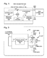
- FIG. 1 is a schematic block diagram of a Free Space Optical (FSO) connector having an optical alignment system.
- the FSO connector 100 comprises an electrical connector 102 having a plurality of contacts 104 for engaging an electronics circuit card connector 106 . Shown are contacts 104 a through 104 n , where n is a variable not limited to any particular value.
- a Small Form-Factor Pluggable (SFP) connector is one example of an electrical connector. However, there are hundreds of other connector types that could likewise enable the device.
- An FSO optical module 108 has at least one optic port 110 for transceiving optical signals 124 via free space. As used herein, “transceiving” means to only transmit, only receive, or both transmit and receive signals.
- a translation module 112 has a connector interface connected to the electrical connector on line 116 and an optical interface connected to FSO module 108 on line 118 .
- the translation module 112 converts electrical signals received via the electrical connector 102 and transferred as optical signals via the optical interface 118 .
- the translation module 112 converts optical signals received via the optical interface 118 and transferred as electrical signals via the electrical connector 102 .
- element 100 may be referred to as an FSO adaptor.
- the FSO optical module 108 has an adjustable mirror 120 for reflecting optical signals, and an adjustable lens 122 for focusing optical signals 124 .
- the mirror is adjustable in the sense that the angle formed by the mirror surface and a fixed reference plane can be modified.
- a controller 126 adjusts the mirror 120 and lens 122 using signals on lines 128 and 130 , respectively, in response to receiving optical alignment acknowledgment signals from a communicating device via the optic port.
- the acknowledgement signals may be electrical signals received via the electrical connector 102 .
- the FSO optical module 108 optimizes optical signals transmitted via the lens 122 and mirror 120 . That is, the lens 122 and mirror 120 are in the transmit path. Alternately, the FSO optical module 108 optimizes optical signals received via the lens 122 and mirror 120 . That is, the lens 122 and mirror 120 are in the receive path. In another aspect, the FSO optical module 108 supports duplex communications, so the signals are transmitted and received in the same path using a time multiplexing scheme. In yet another aspect not shown, the FSO optical module 108 supports independent transmit and receive paths, and there are mirrors and lens in each of the paths.
- the controller 126 sets the lens 122 to an initial wide beam dispersion mode, and sets the mirror 120 to an initial position angle.
- First baud rate optical communications are optimized by iteratively adjusting the mirror and narrowing the lens focus.
- second baud rate optical communications which are faster than the first baud rate, are optimized by iteratively adjusting the mirror and narrowing the lens focus.
- FIGS. 2A through 2C are diagrams depicting an optical signal alignment process.
- the process depicted in FIGS. 2A-2C is applicable to both first and second baud rate communications, although the range of mirror angles and lens focus need not be the same.
- the FSO optical module controller optimizes communications by communicating a sequence of optical alignment signals while adjusting the mirror through a sequence of angles.
- FIG. 2A represents an unfocused laser beam 200 , a photodiode 202 in the receive channel, along with scanning directions 204 and 206 .
- the mirror and lens are in the transmit channel of an FSO connector sending a signal to the photodiode.
- the lens focus is narrowed.
- position 2 and position 3 are the first subsequence.
- the system is not limited to any particular definition of “successful communications”.
- the FSO optical module controller optimizes first baud rate communications by iteratively adjusting the mirror and narrowing the lens focus until a predetermined communications power level is achieved.
- the mirror 120 angles are adjusted through the first subsequence, and after determining a second subsequence of mirror angles associated with successful communications, the lens focus can be narrowed again.
- the second subsequence is a narrower range of angles within the first subsequence.
- the definition of “successful” as applied to the second subsequent may be more restrictive than the definition applied to the first subsequence.
- positions B and C are associated with the second subsequence.
- This mirror-adjust/lens focus process may be reiterated any number of times.
- a median mirror angle is selected from the last subsequence, or last set of subsequences.
- the FSO optical module controller optimizes second baud rate communications by iteratively adjusting the mirror and narrowing the lens focus until a predetermined information error rate is achieved.
- FIG. 3 is a perspective view depicting a variation of mirror adjustment procedure of FIG. 2A or 2 B.
- the FSO optical module controller adjusts the mirror through the sequence of angles by adjusting the mirror through a first sequence of angles associated with a first scan direction 300 , and subsequent to determining a subsequence of the first sequence, adjusts the mirror through a second sequence of angles associated with a second scan direction 302 .
- the “angles” are represented on the receive side by transmitted light patterns. After finding a subset of mirror angles in two dimensions, associated with successful communications, the lens focus can be narrowed. Note: although only two, orthogonal scan directions are depicted, the system may be enabled using three, or more scan directions
- FIG. 4 is a schematic block diagram depicting a network of devices equipped with FSO connectors.
- the FSO optical module controller 126 associated with FSO connector 100 chooses a link for alignment based upon a predetermined priority scheme.
- the priority scheme may be that the device with the lower serial number aligns first.
- the priority may determine that FSO connector 100 is aligned first. If the adjustable mirrors and lens of FSO connector 100 are associated with link 400 , then link 400 is the first to be aligned.
- link to be aligned may be either a receiver channel or transmitter channel, as seen from the perspective of FSO connector 100 .
- link 400 is a transmit channel from the perspective of FSO connector 100 .
- Transmit channel 408 includes a light source 410 and receive channel 412 includes a photodiode 414 .
- FSO connector 404 must either make the same priority determinations as FSO connector 100 in order for the priority scheme to work, or the FSO connectors must operate in a master/slave relationship.
- the unselected link 402 is aligned. Alternately, subsequent to optimizing the first baud rate communications for the selected link 400 , first baud rate communications are optimized for the unselected link 402 . Subsequent to optimizing the second baud rate communications for the selected link 400 , then second baud rate communications for the unselected link are optimized.
- FIG. 5 is a schematic block diagram of a first variation of the FSO connector of FIG. 1 .
- the FSO optical module 108 includes a plurality of optic ports 110 for transceiving optical signals in a corresponding plurality of directions in free space. Shown are optical ports 110 a through 110 p , where p is a variable not limited to any particular value.
- the FSO optical module 108 may transmit and/or receive optical signals along a first axis 200 in free space via port 110 a , and transmit/or and receive optical signals along a second axis 202 in free space via port 110 b .
- the second axis is defined with respect the first axis 200 .
- the second axis is coming out of the page (along the z axis) towards the reader.
- the second axis may be fixed and orthogonal to the first axis.
- the orientation of the first and second axes may be adjustable.
- the FSO optical module 108 may also transmit and receive optical signals along a third axis 204 via free space using port 110 c , and transmit and receive optical signals along a fourth axis via free space using port ( 110 n ).
- the fourth axis and port ( 110 n ) cannot be seen in this view, as they are on the opposite side of the FSO optical module from port 110 b .
- first and third axes may be the same, and the second and fourth axes may be the same.
- first and third axis may be in the same (x) vertical axis, but offset in the (y) horizontal or z axis.
- second and fourth axes may be in the same z axis, but offset in the x or y axis.
- Each of the above-mentioned optic ports 110 ay be associated with an adjustable lens and mirror.
- FIG. 6 is a schematic block diagram depicting the translation module of FIG. 1 in greater detail.
- the translation module 112 converts between electrical signals in a first signal format and optical signals in a second signal format. Alternately, the translation module simply reproduces the pulse frequencies, spacings, durations, or intensities of electrical signals into the equivalent optical signal pulse frequencies, spacings, durations, or intensities. In one aspect, the translation module may condition and filter signals without changing the format.
- the translation module may be used to pre-condition the electrical signals driving the laser, and process the electrical signals recovered by the PD. For example, the electrical signals may be filtered or (re)aligned with a clock. In one aspect, a clock is generated from the received electrical signal, which is output to the line card via the electrical connector 102 . Generally, a received signal requires more processing than a transmitted signal.
- the translation module 112 includes a photodiode (PD) 300 to accept optical signals received by the FSO optical module.
- the PD 300 converts the optical signal to an electrical signal supplied to the electrical connector.
- the translation module 112 may also include a laser 302 to accept electrical signals received via the electrical connector.
- the laser 302 converts the electrical signal to an optical signal supplied to the FSO optical module.
- the laser 302 can be a laser diode.
- FIG. 7 is a perspective drawing of an FSO optical module transceiving in a plurality of directions through the use of adjustable mirrors.
- the translation module supplies four optical signals in a fifth direction 500 .
- the FSO optical module 108 includes a first mirror 502 to accept a first optical signal 504 , and reflect the first optical signal for transmission via free space in the first direction.
- a second mirror 508 accepts a second optical signal 510 and reflects the second optical signal for transmission via free space in the second direction, orthogonal to the first direction 506 .
- a third mirror 514 accepts a third optical signal 516 and reflects the third optical signal for transmission via free space in the third direction, 180 degrees from the first direction 506 (and orthogonal to second direction).
- a fourth mirror ( 520 , not shown) accepts a fourth optical signal 522 and reflects the fourth optical signal for transmission via free space in the fourth direction, 180 degrees from the second direction (and orthogonal to the first and third directions).
- the translation module 112 includes a multifaceted FSO optical interface 118 including a first surface ( 530 , not shown) orthogonal to the first direction to receive a fifth optical signal 531 via free space from the first direction.
- a second surface 532 is orthogonal to the second direction to receive a sixth optical signal 534 via free space from the second direction.
- a third surface 536 is orthogonal to the third direction 518 to receive a seventh optical signal 538 via free space from the third direction.
- a fourth surface ( 540 , not shown) is orthogonal to the fourth direction to receive an eighth optical signal 542 via free space from the fourth direction.
- FIG. 8 is a schematic block diagram of a device with a FSO interface.
- the device 800 may be a circuit card or line card with a (“built-in”) FSO interface 804 and electrical interface 806 connected to a motherboard 808 .
- the built-in FSO interface shares many of the characteristics of the FSO connector shown in FIGS. 1 through 4 , so some explicitly details are skipped in the interest of brevity.
- the device may include a translation interface 802 to convert between electrical signals in the device and optical signals transceived via the FSO optical module 804 .
- the translation interface 802 performs many of the same functions performed by the translation module of FIG. 1 . Alternately, it is possible for the device to process optical signals, in which case a translation module is not necessary.
- the FSO optical module includes an adjustable mirror for reflecting optical signals, an adjustable lens for focusing optical signals, and a controller for sending adjustment signals to the mirror and lens.
- the mirror, lens, and controller are shown in FIG. 1 .
- the controller sets the lens to an initial wide beam dispersion mode, sets the mirror to an initial position angle, optimizes first baud rate optical communications by iteratively adjusting the mirror and narrowing the lens focus. Then, the controller optimizes second baud rate optical communicates, faster than the first baud rate, by iteratively adjusting the mirror and narrowing the lens focus.
- FIG. 9 is a schematic block diagram depicting two line cards, A and B, with established bidirectional FSO communication.
- Each line card deploys laser source 900 , microelectromechanical system (MEMS) mirror 902 , variable focus lens 904 , photodiode 906 , and control logic 908 necessary to maintain and restore the LOS channel.
- MEMS microelectromechanical system
- FIG. 10 illustrates the result of the event that has caused the alignment of the FSO on a line card A to be lost.
- the loss of the signal by Line Card B triggers the invocation of the realignment procedure.
- the following procedure is a variation of the procedure presented above in the description of FIGS. 2A , 2 B, and 3 .
- the instant procedure consists of 2 major phases:
- Each card compares its own ID to the received ID, and the lower priority card transmits a “defer” signal.
- the lower priority card scan space horizontally with the mirror, waiting for a “light” signal indicating that the photodiode of the higher priority card is illuminated. Note: in this aspect, the mirror and lens are in the transmit path.
- the lower priority card records the angle at which the light is initially detected, and continues scanning into the same direction.
- the lower priority card records when the “light” signal is removed, indicating the angle where light is no longer detected.
- the lower priority card After discovering the horizontal and vertical medians, the lower priority card signals the higher priority card using the low baud rate, signaling that it has finished the discovery phase and that the higher priority card may start its discovery phase.
- the higher priority card repeats steps 1 through 5 guided by the feedback from the lower priority card.
- the lower priority card successively narrows the focus of the laser beam while monitoring a “slow” signal from the higher priority card, indicating whether the photodiode is lit.
- the lower priority card diffuses the focus of its beam to the point where the photodiode of the higher priority device is lit again, and the angle discovery procedure is repeated to improve the precision of the angular adjustment.
- FIG. 11 is a flowchart illustrating an exemplary alignment process.
- the process starts with an initialization in Step 1100 .
- a low baud rate (9600 bits per second) is selected, the lens is defocused and the mirror is set to an initial start position (left/down).
- the unit also transmits its identity (MIDo). If the identity of a communicating unit (MIDi) is received in Step 1102 , the process continues to Step 1104 .
- priority is determined by comparing the unit's identity with the received identity. If the unit has higher priority, the process continues to Step 1106 and 1108 , where the unit measures Rx power and returns acknowledgements so that the lower priority can adjust its mirror and lens. Again, it is assumed that the adjustable mirror and lens are located in the transmit channel.
- Step 1110 determines that the lower priority has finished its alignment
- the process goes to Step 1112 .
- a horizontal mirror alignment is preformed in Step 1112 and a vertical alignment is performed Step 1114 .
- Step 1116 the focus of the lens is narrowed. If the target power level or target error rate is achieved in Step 1118 , the alignment process is complete (Step 1120 ) and the unit begins normal operation in Step 1122 .
- FIG. 12A illustrates details of the horizontal alignment step, Step 1112 of FIG. 11 .
- Step 1112 a the unit aligning its mirror and lens begins moving (scanning) the mirror towards the “left”. If feedback is received from the communicating unit (Step 1112 b ) that the optical signal is not being received, then the angle is increased (the scan continues left) in Step 1112 c . Once the feedback indicates the reception of an optical signal, the associated mirror position is stored in Step 1112 d . In Steps 1112 e through 1112 h , the procedure is repeated to the “right”. The average of the right and left mirror positions is determined in Step 1112 i
- FIG. 12B illustrates details of the vertical alignment step, Step 1114 of FIG. 11 .
- Step 1114 a the unit aligning its mirror and lens begins moving (scanning) the mirror “down”. If feedback is received from the communicating unit (Step 1114 b ) that the optical signal is not being received, then the angle is increased (the scan continues down) in Step 1114 c . Once the feedback indicates the reception of a signal, the associated mirror position is stored in Step 1114 d . In Steps 1114 e through 1114 h , the procedure is repeated scanning “up”. The average of the down and up mirror positions is determined in Step 1114 i
- FIG. 13 is a flowchart illustrating a method for aligning the optic port of a device having an FSO connector. Although the method is depicted as a sequence of numbered steps for clarity, the numbering does not necessarily dictate the order of the steps. It should be understood that some of these steps may be skipped, performed in parallel, or performed without the requirement of maintaining a strict order of sequence.
- the method starts at Step 1200 .
- a controller determines in Step 1202 that an optic port alignment procedure is required.
- Step 1204 sets a lens to an initial wide beam dispersion mode.
- Step 1206 sets a mirror to an initial position angle.
- Step 1208 communicates an optical signal at a first low baud rate.
- Step 1210 optimizes first baud rate communications by iteratively adjusting the mirror and narrowing the lens focus. In one aspect, Step 1210 iteratively adjusts the mirror and narrows the lens focus until a predetermined communications power level is achieved.
- Step 1212 communicates an optical signal at a second baud rate, faster than the first baud rate.
- Step 1214 optimizes second baud rate communications by iteratively adjusting the mirror and narrowing the lens focus. In one aspect, Step 1214 iteratively adjusts the mirror and narrows the lens focus until a predetermined information error rate is achieved.
- Optimizing the first baud rate signals in Step 1210 or optimizing the second baud rate optical signals in Step 1214 means that the optical signals being transmitted to a link partner are optimized, and that optical signal acknowledgements to the transmissions are received from the link partner. That is, the mirror and lens are in the transmit channel. Alternately, the mirror and lens are in the receive channel, and the optical signals received from a link partner are optimized while optical signal acknowledgements are transmitted to the link partner.
- optimizing first and second baud rate communications includes substeps.
- the substeps are shown associated with Step 1214 . These same substeps could be shown associated with Step 1210 , but have been omitted in the interest of brevity.
- Step 1214 a communicates a sequence of optical alignment signals while adjusting the mirror through a sequence of angles.
- Step 1214 b determines a subsequence of mirror angles associated with successful communications.
- Step 1214 c narrows the lens focus, and the arrow labeled with reference designator 1214 d indicates that the above-described steps (Steps 1214 a - 1214 c ) of adjusting the mirror angles, determining mirror angles associated with successful communications, and narrowing the focus can be reiterated.
- adjusting the mirror through the sequence of angles in Step 1214 a includes additional substeps.
- Step 1214 a 1 adjusts the mirror through a first sequence of angles associated with a first scan direction.
- Step 1214 a 2 adjusts the mirror through a second sequence of angles associated with a second scan direction.
- determining that the optic port alignment procedure is required in Step 1202 means that the step is initiated in response to failing to successfully receive communications from a link partner, or receiving messages indicating that the link partner is failing to successfully receive messages.
- determining that the optic port alignment procedure is required in Step 1202 includes choosing a link for alignment based upon a predetermined priority scheme, where the link is either a receiver channel or a transmitter channel. Then, subsequent to optimizing the second baud rate communications for the selected link in Step 1214 , Step 1216 aligns the unselected link.
- Step 1211 optimizes first baud rate communications for the unselected link subsequent to optimizing the first baud rate communications for the selected link in Step 1210 .
- optimizing the second baud rate communications in Step 1214 includes optimizing second baud rate communications for the selected link, subsequent to optimizing the first baud rate communications for the unselected link (Step 1211 ). Subsequent to optimizing the second baud Tate communications for the selected link in Step 1214 , Step 1216 optimizes second baud rate communications for the unselected link.
Abstract
Description
Claims (19)
Priority Applications (1)
| Application Number | Priority Date | Filing Date | Title |
|---|---|---|---|
| US12/563,962 US8200094B1 (en) | 2009-04-11 | 2009-09-21 | System and method for free space optical connector alignment |
Applications Claiming Priority (2)
| Application Number | Priority Date | Filing Date | Title |
|---|---|---|---|
| US12/422,265 US8135281B2 (en) | 2009-04-11 | 2009-04-11 | Free space optical connector |
| US12/563,962 US8200094B1 (en) | 2009-04-11 | 2009-09-21 | System and method for free space optical connector alignment |
Related Parent Applications (1)
| Application Number | Title | Priority Date | Filing Date |
|---|---|---|---|
| US12/422,265 Continuation-In-Part US8135281B2 (en) | 2009-04-11 | 2009-04-11 | Free space optical connector |
Publications (1)
| Publication Number | Publication Date |
|---|---|
| US8200094B1 true US8200094B1 (en) | 2012-06-12 |
Family
ID=46177857
Family Applications (1)
| Application Number | Title | Priority Date | Filing Date |
|---|---|---|---|
| US12/563,962 Expired - Fee Related US8200094B1 (en) | 2009-04-11 | 2009-09-21 | System and method for free space optical connector alignment |
Country Status (1)
| Country | Link |
|---|---|
| US (1) | US8200094B1 (en) |
Cited By (10)
| Publication number | Priority date | Publication date | Assignee | Title |
|---|---|---|---|---|
| US20130082162A1 (en) * | 2010-03-16 | 2013-04-04 | Jan Eide | Method of Directing an Optical Receiver Toward a Light Source and an Apparatus of Practising the Method |
| US20140064739A1 (en) * | 2012-08-28 | 2014-03-06 | Industrial Technology Research Institute | Light communication system, transmitter and receiver |
| WO2014184616A1 (en) * | 2013-05-14 | 2014-11-20 | Nokia Corporation | Alignment of optical devices |
| US20150288477A1 (en) * | 2012-12-17 | 2015-10-08 | Huawei Technologies Co., Ltd. | Line Card, Optical Module, and Optical Network Device |
| US9816856B2 (en) | 2015-12-17 | 2017-11-14 | Harris Corporation | Magnetically coupled optical connector assembly and related methods |
| CN111327360A (en) * | 2018-12-13 | 2020-06-23 | 财团法人工业技术研究院 | Scanning type optical antenna and control method thereof |
| US10924186B1 (en) * | 2019-12-03 | 2021-02-16 | Netgami System L.L.C. | Optical fiber link for remote low power sensor solution |
| US11303357B1 (en) * | 2021-03-08 | 2022-04-12 | Mellanox Technologies Tlv Ltd. | Systems, methods, and devices for optical assemblies |
| US11329721B2 (en) * | 2020-06-09 | 2022-05-10 | Tamron Co., Ltd. | Communication device, optical axis direction adjusting method, and communication system |
| US11502753B2 (en) * | 2017-09-28 | 2022-11-15 | Kyocera Sld Laser, Inc. | Intelligent visible light with a gallium and nitrogen containing laser source |
Citations (29)
| Publication number | Priority date | Publication date | Assignee | Title |
|---|---|---|---|---|
| US4823402A (en) * | 1986-04-21 | 1989-04-18 | Trw Inc. | Agile optical beam steering system |
| US5347387A (en) * | 1992-03-24 | 1994-09-13 | Rice Robert C | Self-aligning optical transceiver |
| US5448391A (en) * | 1992-06-30 | 1995-09-05 | Sony Corporation | Optical atmospheric link system |
| US5594580A (en) * | 1993-11-16 | 1997-01-14 | Canon Kabushiki Kaisha | Optical space communication apparatus |
| US5684614A (en) * | 1995-01-26 | 1997-11-04 | Canon Kabushiki Kaisha | Optical space communication apparatus |
| US5770850A (en) * | 1997-04-30 | 1998-06-23 | At&T Corp | Sensor array tracking and detection system having an alignment positioner |
| US5867294A (en) * | 1993-09-24 | 1999-02-02 | Canon Kabushiki Kaisha | Optical space communication apparatus |
| US6122084A (en) * | 1998-03-03 | 2000-09-19 | At&T Corp. | High dynamic range free-space optical communication receiver |
| US6335811B1 (en) * | 1997-10-24 | 2002-01-01 | Canon Kabushiki Kaisha | Optical space communication apparatus |
| US20020131121A1 (en) * | 2001-03-13 | 2002-09-19 | Muthu Jeganathan | Transceiver, system, and method for free-space optical communication and tracking |
| US6493122B1 (en) * | 1997-09-09 | 2002-12-10 | Canon Kabushiki Kaisha | Optical space communication apparatus |
| US20020196506A1 (en) * | 2001-06-26 | 2002-12-26 | Zyoptics, Inc. | Atmospheric optical data transmission system |
| US6510401B2 (en) * | 2001-05-11 | 2003-01-21 | The United States Of America As Represented By The Director Of The National Security Agency | Method of authenticating beacon |
| US6577421B1 (en) * | 1999-08-12 | 2003-06-10 | Hughes Electronics Corporation | Alignment system and method for optical satellite communication |
| US20040052465A1 (en) * | 2002-09-12 | 2004-03-18 | Alcatel | Receiver for a free space optics system which is able to evaluate the causes of a reduction of the received power |
| US20040208597A1 (en) * | 2002-07-30 | 2004-10-21 | Wittenberger John C. | Free-Space optical transceiver link |
| US6821029B1 (en) * | 2002-09-10 | 2004-11-23 | Xilinx, Inc. | High speed serial I/O technology using an optical link |
| US20040258415A1 (en) * | 2003-06-18 | 2004-12-23 | Boone Bradley G. | Techniques for secure free space laser communications |
| US6856437B2 (en) * | 2002-02-01 | 2005-02-15 | Terabeam Corporation | Fast steering mirror |
| US6894818B1 (en) * | 2003-11-25 | 2005-05-17 | Northrop Grumman Corporation | Conformal all-reflective beam-steering (CARBS) device |
| US20050276610A1 (en) * | 2004-05-25 | 2005-12-15 | Tomoshi Hirayama | Contents-delivery system, contents-transmission device, contents-reception device, and contents-delivery method |
| US20060018661A1 (en) * | 2002-03-04 | 2006-01-26 | Green Edward A | Alignment system |
| US7263297B2 (en) * | 2002-10-18 | 2007-08-28 | Alcatel | Method and device for the control of the power radiated onto a transmission telescope in free-space laser telecommunications systems |
| US7292788B2 (en) * | 2003-01-31 | 2007-11-06 | Lockheed Martin Corporation | Multi-beam laser communications system and method |
| US7343099B2 (en) * | 2004-02-12 | 2008-03-11 | Metrologic Instruments, Inc. | Free space optical (FSO) laser communication system employing fade mitigation measures based on laser beam speckle tracking and locking principles |
| US20090028579A1 (en) * | 2007-07-23 | 2009-01-29 | Finisar Corporation | Fiber optic link having an integrated laser and photodetector chip |
| US7565082B2 (en) * | 2004-08-27 | 2009-07-21 | Kddi Corporation | Data transmission method and system thereof, portable terminal, and data receiver |
| US7593641B2 (en) * | 2003-11-10 | 2009-09-22 | Harris Corporation | System and method of free-space optical satellite communications |
| US7643755B2 (en) * | 2003-10-13 | 2010-01-05 | Noble Peak Vision Corp. | Optical receiver comprising a receiver photodetector integrated with an imaging array |
-
2009
- 2009-09-21 US US12/563,962 patent/US8200094B1/en not_active Expired - Fee Related
Patent Citations (29)
| Publication number | Priority date | Publication date | Assignee | Title |
|---|---|---|---|---|
| US4823402A (en) * | 1986-04-21 | 1989-04-18 | Trw Inc. | Agile optical beam steering system |
| US5347387A (en) * | 1992-03-24 | 1994-09-13 | Rice Robert C | Self-aligning optical transceiver |
| US5448391A (en) * | 1992-06-30 | 1995-09-05 | Sony Corporation | Optical atmospheric link system |
| US5867294A (en) * | 1993-09-24 | 1999-02-02 | Canon Kabushiki Kaisha | Optical space communication apparatus |
| US5594580A (en) * | 1993-11-16 | 1997-01-14 | Canon Kabushiki Kaisha | Optical space communication apparatus |
| US5684614A (en) * | 1995-01-26 | 1997-11-04 | Canon Kabushiki Kaisha | Optical space communication apparatus |
| US5770850A (en) * | 1997-04-30 | 1998-06-23 | At&T Corp | Sensor array tracking and detection system having an alignment positioner |
| US6493122B1 (en) * | 1997-09-09 | 2002-12-10 | Canon Kabushiki Kaisha | Optical space communication apparatus |
| US6335811B1 (en) * | 1997-10-24 | 2002-01-01 | Canon Kabushiki Kaisha | Optical space communication apparatus |
| US6122084A (en) * | 1998-03-03 | 2000-09-19 | At&T Corp. | High dynamic range free-space optical communication receiver |
| US6577421B1 (en) * | 1999-08-12 | 2003-06-10 | Hughes Electronics Corporation | Alignment system and method for optical satellite communication |
| US20020131121A1 (en) * | 2001-03-13 | 2002-09-19 | Muthu Jeganathan | Transceiver, system, and method for free-space optical communication and tracking |
| US6510401B2 (en) * | 2001-05-11 | 2003-01-21 | The United States Of America As Represented By The Director Of The National Security Agency | Method of authenticating beacon |
| US20020196506A1 (en) * | 2001-06-26 | 2002-12-26 | Zyoptics, Inc. | Atmospheric optical data transmission system |
| US6856437B2 (en) * | 2002-02-01 | 2005-02-15 | Terabeam Corporation | Fast steering mirror |
| US20060018661A1 (en) * | 2002-03-04 | 2006-01-26 | Green Edward A | Alignment system |
| US20040208597A1 (en) * | 2002-07-30 | 2004-10-21 | Wittenberger John C. | Free-Space optical transceiver link |
| US6821029B1 (en) * | 2002-09-10 | 2004-11-23 | Xilinx, Inc. | High speed serial I/O technology using an optical link |
| US20040052465A1 (en) * | 2002-09-12 | 2004-03-18 | Alcatel | Receiver for a free space optics system which is able to evaluate the causes of a reduction of the received power |
| US7263297B2 (en) * | 2002-10-18 | 2007-08-28 | Alcatel | Method and device for the control of the power radiated onto a transmission telescope in free-space laser telecommunications systems |
| US7292788B2 (en) * | 2003-01-31 | 2007-11-06 | Lockheed Martin Corporation | Multi-beam laser communications system and method |
| US20040258415A1 (en) * | 2003-06-18 | 2004-12-23 | Boone Bradley G. | Techniques for secure free space laser communications |
| US7643755B2 (en) * | 2003-10-13 | 2010-01-05 | Noble Peak Vision Corp. | Optical receiver comprising a receiver photodetector integrated with an imaging array |
| US7593641B2 (en) * | 2003-11-10 | 2009-09-22 | Harris Corporation | System and method of free-space optical satellite communications |
| US6894818B1 (en) * | 2003-11-25 | 2005-05-17 | Northrop Grumman Corporation | Conformal all-reflective beam-steering (CARBS) device |
| US7343099B2 (en) * | 2004-02-12 | 2008-03-11 | Metrologic Instruments, Inc. | Free space optical (FSO) laser communication system employing fade mitigation measures based on laser beam speckle tracking and locking principles |
| US20050276610A1 (en) * | 2004-05-25 | 2005-12-15 | Tomoshi Hirayama | Contents-delivery system, contents-transmission device, contents-reception device, and contents-delivery method |
| US7565082B2 (en) * | 2004-08-27 | 2009-07-21 | Kddi Corporation | Data transmission method and system thereof, portable terminal, and data receiver |
| US20090028579A1 (en) * | 2007-07-23 | 2009-01-29 | Finisar Corporation | Fiber optic link having an integrated laser and photodetector chip |
Cited By (18)
| Publication number | Priority date | Publication date | Assignee | Title |
|---|---|---|---|---|
| US8805192B2 (en) * | 2010-03-16 | 2014-08-12 | Polewall As | Method of directing an optical receiver toward a light source and an apparatus of practicing the method |
| US20130082162A1 (en) * | 2010-03-16 | 2013-04-04 | Jan Eide | Method of Directing an Optical Receiver Toward a Light Source and an Apparatus of Practising the Method |
| US20140064739A1 (en) * | 2012-08-28 | 2014-03-06 | Industrial Technology Research Institute | Light communication system, transmitter and receiver |
| CN103684586A (en) * | 2012-08-28 | 2014-03-26 | 财团法人工业技术研究院 | Optical communication system, transmitter and receiver |
| CN103684586B (en) * | 2012-08-28 | 2016-03-23 | 财团法人工业技术研究院 | Optical communication system, transmitter and receiver |
| US9312954B2 (en) * | 2012-08-28 | 2016-04-12 | Industrial Technology Research Institute | Light communication system, transmitter and receiver |
| US20150288477A1 (en) * | 2012-12-17 | 2015-10-08 | Huawei Technologies Co., Ltd. | Line Card, Optical Module, and Optical Network Device |
| US9838147B2 (en) * | 2012-12-17 | 2017-12-05 | Huawei Technologies Co., Ltd. | Line card, optical module, and optical network device |
| US9929806B2 (en) | 2013-05-14 | 2018-03-27 | Nokia Technologies Oy | Alignment of optical devices |
| WO2014184616A1 (en) * | 2013-05-14 | 2014-11-20 | Nokia Corporation | Alignment of optical devices |
| US9816856B2 (en) | 2015-12-17 | 2017-11-14 | Harris Corporation | Magnetically coupled optical connector assembly and related methods |
| US11502753B2 (en) * | 2017-09-28 | 2022-11-15 | Kyocera Sld Laser, Inc. | Intelligent visible light with a gallium and nitrogen containing laser source |
| US11870495B2 (en) | 2017-09-28 | 2024-01-09 | Kyocera Sld Laser, Inc. | Intelligent visible light with a gallium and nitrogen containing laser source |
| CN111327360A (en) * | 2018-12-13 | 2020-06-23 | 财团法人工业技术研究院 | Scanning type optical antenna and control method thereof |
| CN111327360B (en) * | 2018-12-13 | 2021-10-08 | 财团法人工业技术研究院 | Scanning type optical antenna and control method thereof |
| US10924186B1 (en) * | 2019-12-03 | 2021-02-16 | Netgami System L.L.C. | Optical fiber link for remote low power sensor solution |
| US11329721B2 (en) * | 2020-06-09 | 2022-05-10 | Tamron Co., Ltd. | Communication device, optical axis direction adjusting method, and communication system |
| US11303357B1 (en) * | 2021-03-08 | 2022-04-12 | Mellanox Technologies Tlv Ltd. | Systems, methods, and devices for optical assemblies |
Similar Documents
| Publication | Publication Date | Title |
|---|---|---|
| US8200094B1 (en) | System and method for free space optical connector alignment | |
| US8135281B2 (en) | Free space optical connector | |
| US7941053B2 (en) | Optical transceiver for 40 gigabit/second transmission | |
| US7581891B2 (en) | Laser adjustment in integrated optoelectronic modules/fiber optic cables | |
| US8625989B2 (en) | Multi-laser transmitter optical subassemblies for optoelectronic modules | |
| US8200097B2 (en) | Optoelectronic module form-factor adapter | |
| EP2816677B1 (en) | Combined optical and electrical interface | |
| US6951426B2 (en) | Pad architecture for backwards compatibility for bi-directional transceiver module | |
| US7970283B2 (en) | High speed SFP transceiver | |
| US20190007132A1 (en) | Client protection switch in optical pluggable transceivers activated through fast electrical data squelch | |
| JP2007534988A (en) | Modular optical device package | |
| CA2357660C (en) | Method and apparatus for aligning telescopes within a free-space optical communication system | |
| US20070098405A1 (en) | Method and system for bi-directional communication over a single optical fiber | |
| US7044656B1 (en) | Adapter for interoperability between optical transceiver and legacy components | |
| US9011022B2 (en) | Combined optical and electrical interface | |
| CN103152103A (en) | Optical module and adaptive regulation method for rate mode of clock and data recovery (CDR) chip of optical module | |
| US20040161240A1 (en) | Module having two bi-directional optical transceivers | |
| US20140072305A1 (en) | Method and system for bi-directional communication over a single optical fiber | |
| WO2017162146A1 (en) | Method and device for realizing inter-board communication | |
| US10855041B2 (en) | Optical to electrical adapter | |
| US7502533B2 (en) | Mechanism for conditioning launched beams from an optical transmitter | |
| Lemoff et al. | A compact, low-cost WDM transceiver for the LAN | |
| Drogemuller et al. | Current progress of advanced high speed parallel optical links for computer clusters and switching systems | |
| EP4205307A1 (en) | A pluggable connector for use in an optical wireless communication system | |
| US20030035180A1 (en) | Installation of processing units into a stored program controlled system wherein the component processing units are interconnected via free space optics |
Legal Events
| Date | Code | Title | Description |
|---|---|---|---|
| AS | Assignment |
Owner name: APPLIED MICRO CIRCUITS CORPORATION, CALIFORNIA Free format text: ASSIGNMENT OF ASSIGNORS INTEREST;ASSIGNORS:ZHOVNIROVSKY, IGOR;ROY, SUBHASH;REEL/FRAME:023261/0018 Effective date: 20090918 |
|
| STCF | Information on status: patent grant |
Free format text: PATENTED CASE |
|
| AS | Assignment |
Owner name: VOLEX PLC, UNITED KINGDOM Free format text: 50 PERCENT INTEREST;ASSIGNOR:APPLIED MICRO CIRCUITS CORPORATION;REEL/FRAME:029594/0696 Effective date: 20121220 |
|
| FPAY | Fee payment |
Year of fee payment: 4 |
|
| AS | Assignment |
Owner name: APPLIED MICRO CIRCUITS CORPORATION, CALIFORNIA Free format text: ASSIGNMENT OF ASSIGNORS INTEREST;ASSIGNOR:VOLEX PLC;REEL/FRAME:040344/0160 Effective date: 20161010 |
|
| FEPP | Fee payment procedure |
Free format text: PAYOR NUMBER ASSIGNED (ORIGINAL EVENT CODE: ASPN); ENTITY STATUS OF PATENT OWNER: LARGE ENTITY |
|
| AS | Assignment |
Owner name: MACOM CONNECTIVITY SOLUTIONS, LLC, MASSACHUSETTS Free format text: MERGER AND CHANGE OF NAME;ASSIGNORS:APPLIED MICRO CIRCUITS CORPORATION;MACOM CONNECTIVITY SOLUTIONS, LLC;REEL/FRAME:042423/0700 Effective date: 20170126 |
|
| AS | Assignment |
Owner name: GOLDMAN SACHS BANK USA, AS COLLATERAL AGENT, NEW Y Free format text: SECURITY INTEREST;ASSIGNOR:MACOM CONNECTIVITY SOLUTIONS, LLC (SUCCESSOR TO APPLIED MICRO CIRCUITS CORPORATION);REEL/FRAME:042444/0891 Effective date: 20170504 Owner name: GOLDMAN SACHS BANK USA, AS COLLATERAL AGENT, NEW YORK Free format text: SECURITY INTEREST;ASSIGNOR:MACOM CONNECTIVITY SOLUTIONS, LLC (SUCCESSOR TO APPLIED MICRO CIRCUITS CORPORATION);REEL/FRAME:042444/0891 Effective date: 20170504 |
|
| FEPP | Fee payment procedure |
Free format text: MAINTENANCE FEE REMINDER MAILED (ORIGINAL EVENT CODE: REM.); ENTITY STATUS OF PATENT OWNER: LARGE ENTITY |
|
| LAPS | Lapse for failure to pay maintenance fees |
Free format text: PATENT EXPIRED FOR FAILURE TO PAY MAINTENANCE FEES (ORIGINAL EVENT CODE: EXP.); ENTITY STATUS OF PATENT OWNER: LARGE ENTITY |
|
| STCH | Information on status: patent discontinuation |
Free format text: PATENT EXPIRED DUE TO NONPAYMENT OF MAINTENANCE FEES UNDER 37 CFR 1.362 |
|
| FP | Lapsed due to failure to pay maintenance fee |
Effective date: 20200612 |