US8230300B2 - Efficient readout from analog memory cells using data compression - Google Patents
Efficient readout from analog memory cells using data compression Download PDFInfo
- Publication number
- US8230300B2 US8230300B2 US12/397,368 US39736809A US8230300B2 US 8230300 B2 US8230300 B2 US 8230300B2 US 39736809 A US39736809 A US 39736809A US 8230300 B2 US8230300 B2 US 8230300B2
- Authority
- US
- United States
- Prior art keywords
- storage values
- confidence levels
- output storage
- ecc
- memory cells
- Prior art date
- Legal status (The legal status is an assumption and is not a legal conclusion. Google has not performed a legal analysis and makes no representation as to the accuracy of the status listed.)
- Active, expires
Links
- 230000015654 memory Effects 0.000 title claims abstract description 194
- 238000013144 data compression Methods 0.000 title 1
- 238000000034 method Methods 0.000 claims abstract description 52
- 238000013500 data storage Methods 0.000 claims abstract description 10
- 230000011664 signaling Effects 0.000 claims description 19
- 238000012546 transfer Methods 0.000 claims description 14
- 238000007670 refining Methods 0.000 claims description 13
- 238000012937 correction Methods 0.000 claims description 7
- 230000006835 compression Effects 0.000 description 24
- 238000007906 compression Methods 0.000 description 24
- 238000009826 distribution Methods 0.000 description 13
- 238000004891 communication Methods 0.000 description 9
- 230000008569 process Effects 0.000 description 5
- 230000006837 decompression Effects 0.000 description 4
- 238000003491 array Methods 0.000 description 2
- 230000008901 benefit Effects 0.000 description 2
- 230000008859 change Effects 0.000 description 2
- 238000006243 chemical reaction Methods 0.000 description 2
- 238000010586 diagram Methods 0.000 description 2
- 238000007667 floating Methods 0.000 description 2
- 230000006870 function Effects 0.000 description 2
- 238000004377 microelectronic Methods 0.000 description 2
- 239000007787 solid Substances 0.000 description 2
- LZIAMMQBHJIZAG-UHFFFAOYSA-N 2-[di(propan-2-yl)amino]ethyl carbamimidothioate Chemical compound CC(C)N(C(C)C)CCSC(N)=N LZIAMMQBHJIZAG-UHFFFAOYSA-N 0.000 description 1
- 206010011906 Death Diseases 0.000 description 1
- 230000003679 aging effect Effects 0.000 description 1
- 230000009286 beneficial effect Effects 0.000 description 1
- 238000004364 calculation method Methods 0.000 description 1
- 230000001413 cellular effect Effects 0.000 description 1
- 230000006735 deficit Effects 0.000 description 1
- 238000005516 engineering process Methods 0.000 description 1
- 238000012804 iterative process Methods 0.000 description 1
- 239000000463 material Substances 0.000 description 1
- 238000012986 modification Methods 0.000 description 1
- 230000004048 modification Effects 0.000 description 1
- 150000004767 nitrides Chemical class 0.000 description 1
- 230000003287 optical effect Effects 0.000 description 1
- 230000004044 response Effects 0.000 description 1
- 239000004065 semiconductor Substances 0.000 description 1
- 238000012163 sequencing technique Methods 0.000 description 1
Images


Classifications
-
- G—PHYSICS
- G06—COMPUTING; CALCULATING OR COUNTING
- G06F—ELECTRIC DIGITAL DATA PROCESSING
- G06F3/00—Input arrangements for transferring data to be processed into a form capable of being handled by the computer; Output arrangements for transferring data from processing unit to output unit, e.g. interface arrangements
- G06F3/06—Digital input from, or digital output to, record carriers, e.g. RAID, emulated record carriers or networked record carriers
- G06F3/0601—Interfaces specially adapted for storage systems
- G06F3/0628—Interfaces specially adapted for storage systems making use of a particular technique
- G06F3/0638—Organizing or formatting or addressing of data
-
- G—PHYSICS
- G06—COMPUTING; CALCULATING OR COUNTING
- G06F—ELECTRIC DIGITAL DATA PROCESSING
- G06F11/00—Error detection; Error correction; Monitoring
- G06F11/07—Responding to the occurrence of a fault, e.g. fault tolerance
- G06F11/08—Error detection or correction by redundancy in data representation, e.g. by using checking codes
- G06F11/10—Adding special bits or symbols to the coded information, e.g. parity check, casting out 9's or 11's
- G06F11/1008—Adding special bits or symbols to the coded information, e.g. parity check, casting out 9's or 11's in individual solid state devices
-
- G—PHYSICS
- G06—COMPUTING; CALCULATING OR COUNTING
- G06F—ELECTRIC DIGITAL DATA PROCESSING
- G06F12/00—Accessing, addressing or allocating within memory systems or architectures
- G06F12/02—Addressing or allocation; Relocation
- G06F12/08—Addressing or allocation; Relocation in hierarchically structured memory systems, e.g. virtual memory systems
-
- G—PHYSICS
- G06—COMPUTING; CALCULATING OR COUNTING
- G06F—ELECTRIC DIGITAL DATA PROCESSING
- G06F3/00—Input arrangements for transferring data to be processed into a form capable of being handled by the computer; Output arrangements for transferring data from processing unit to output unit, e.g. interface arrangements
- G06F3/06—Digital input from, or digital output to, record carriers, e.g. RAID, emulated record carriers or networked record carriers
- G06F3/0601—Interfaces specially adapted for storage systems
- G06F3/0602—Interfaces specially adapted for storage systems specifically adapted to achieve a particular effect
- G06F3/0604—Improving or facilitating administration, e.g. storage management
-
- G—PHYSICS
- G06—COMPUTING; CALCULATING OR COUNTING
- G06F—ELECTRIC DIGITAL DATA PROCESSING
- G06F3/00—Input arrangements for transferring data to be processed into a form capable of being handled by the computer; Output arrangements for transferring data from processing unit to output unit, e.g. interface arrangements
- G06F3/06—Digital input from, or digital output to, record carriers, e.g. RAID, emulated record carriers or networked record carriers
- G06F3/0601—Interfaces specially adapted for storage systems
- G06F3/0668—Interfaces specially adapted for storage systems adopting a particular infrastructure
- G06F3/0671—In-line storage system
- G06F3/0673—Single storage device
- G06F3/0679—Non-volatile semiconductor memory device, e.g. flash memory, one time programmable memory [OTP]
Definitions
- the present invention relates generally to memory devices, and particularly to methods and systems for reading data from analog memory cells.
- Flash memories use arrays of analog memory cells for storing data.
- Each analog memory cell holds a certain level of a given physical quantity such as an electrical charge or voltage, which represents the data stored in the cell. The levels of this physical quantity are also referred to as storage values or analog values.
- each analog memory cell holds a certain amount of electrical charge.
- the range of possible analog values is typically divided into regions, each region corresponding to a programming state that represents one or more data bit values. Data is written to an analog memory cell by writing a nominal analog value that corresponds to the desired bit or bits.
- Some memory devices which are commonly referred to as Single-Level Cell (SLC) devices, store a single bit of information in each memory cell, i.e., each memory cell can be programmed to assume two possible memory states.
- SLC Single-Level Cell
- MLC Multi-Level Cell
- MLC Multi-Level Cell
- Flash memory devices are described, for example, by Bez et al., in “Introduction to Flash Memory,” Proceedings of the IEEE, volume 91, number 4, April, 2003, pages 489-502, which is incorporated herein by reference.
- Multi-level Flash cells and devices are described, for example, by Eitan et al., in “Multilevel Flash Cells and their Trade-Offs,” Proceedings of the 1996 IEEE International Electron Devices Meeting (IEDM), New York, N.Y., pages 169-172, which is incorporated herein by reference.
- the paper compares several kinds of multilevel Flash cells, such as common ground, DINOR, AND, NOR and NAND cells.
- NROM Nitride Read Only Memory
- SSDM Solid State Devices and Materials
- FG Floating Gate
- FRAM Ferroelectric RAM
- MRAM magnetic RAM
- CTF Charge Trap Flash
- PRAM phase change RAM
- FRAM, MRAM and PRAM cells are described, for example, by Kim and Koh in “Future Memory Technology including Emerging New Memories,” Proceedings of the 24 th International Conference on Microelectronics (MIEL), Nis, Serbia and Montenegro, May 16-19, 2004, volume 1, pages 377-384, which is incorporated herein by reference.
- Data is sometimes read from memory cells using quality measures.
- U.S. Pat. No. 6,751,766 whose disclosure is incorporated herein by reference, describes a memory system.
- the quality of data stored in the memory system is assessed by different methods, and the memory system is operated according to the assessed quality.
- the data quality can be assessed during read operations.
- Subsequent use of an Error Correction Code (ECC) can utilize the quality indications to detect and reconstruct the data with improved effectiveness.
- ECC Error Correction Code
- a statistics of data quality can be constructed and digital data values can be associated in a modified manner to prevent data corruption. In both cases, corrective actions can be implemented specifically on the poor quality data, according to suitably chosen schedules, and with improved effectiveness because of the knowledge provided by the quality indications.
- An embodiment of the present invention provides a method for data storage, including:
- the method further includes decompressing the transferred output storage values at the memory controller, and reconstructing the data responsively to the output storage values and the decompressed confidence levels.
- storing the data includes encoding the data with an Error Correction Code (ECC), and reconstructing the data includes decoding the ECC responsively to the decompressed confidence levels.
- ECC Error Correction Code
- Decoding the ECC may include computing respective ECC metrics of the output storage values responsively to the confidence levels, and decoding the ECC responsively to the ECC metrics.
- the method includes refining at least some of the confidence levels, updating the ECC metrics based on the refined confidence levels and re-decoding the ECC responsively to the updated ECC metrics.
- Refining the confidence levels and updating the ECC metrics may include, at a first time, refining the confidence levels and updating the ECC metrics only responsively to a failure in decoding the ECC, and at a second time subsequent to the first time, refining the confidence levels and updating the ECC metrics before initially attempting to decode the ECC.
- refining the confidence levels includes refining the confidence levels of only a subset of the output storage values that were previously identified as having a low confidence level.
- computing the ECC metrics includes marking some of the output storage values as erasures.
- reading the output storage values includes applying one or more first read thresholds to the analog memory cells in the group, and estimating the confidence levels includes re-reading the analog memory cells in the group using one or more second read thresholds, different from the first read thresholds.
- storing the data includes programming each of the analog memory cells in the group to a respective programming state selected from two or more programming states, and re-reading the analog memory cells includes identifying the output storage values contained in a boundary region separating two of the programming states.
- reading the output storage values includes re-reading the output storage values multiple times to produce respective multiple sets of read results, and estimating the confidence levels includes determining differences between the respective read results in the multiple sets.
- Re-reading the output storage values may include producing a first set of the read results using a first read operation having a first accuracy level, and producing a second set of the read results using a second read operation having a second accuracy level, finer than the first accuracy level.
- estimating the confidence levels includes assigning some of the output storage value a low confidence level, and compressing and transferring the confidence levels include indicating to the memory controller only the output storage values having the low confidence level.
- the interface includes a parallel bus having a signaling line, transferring the output storage values includes sending one or more of the output storage values during each cycle of the bus, and indicating the storage values having the low confidence level includes signaling over the signaling line when at least one of the output storage values sent during a given cycle has the low confidence level.
- the interface includes a parallel bus having a signaling line, indicating the storage values having the low confidence level includes sending the storage values having the low confidence level over the signaling line, and transferring the output storage values includes sending the output storage values over lines other than the signaling line.
- apparatus for data storage including:
- circuitry which is coupled to store data in a group of the analog memory cells by writing respective input storage values to the memory cells in the group, to read respective output storage values from the analog memory cells in the group after storing the data, to estimate respective confidence levels of the output storage values, to compress the confidence levels, and to transfer the output storage values and the compressed confidence levels from the memory cells over an interface to a memory controller.
- apparatus for data storage including:
- a memory device including:
- a memory controller which is configured to receive the output storage values and the compressed confidence levels over the interface, to decompress the transferred output storage values and to reconstruct the data responsively to the output storage values and the decompressed confidence levels.
- FIG. 1 is a block diagram that schematically illustrates a memory system, in accordance with an embodiment of the present invention
- FIG. 2 is a graph showing storage value distributions in a group of analog memory cells, in accordance with an embodiment of the present invention.
- FIGS. 3 and 4 are flow charts that schematically illustrate methods for data readout from analog memory cells, in accordance with embodiments of the present invention.
- Data is typically stored in analog memory cells by writing respective storage values to the cells.
- the storage operation programs each memory cell to one of several programming states, which represent respective data values.
- Data that is stored in analog memory cells may have varying levels of confidence, i.e., different likelihoods that the data read from the memory cells truly reflects the data that was stored in the cells.
- the storage values (e.g., threshold voltages) of the memory cells that are associated with a given programming state have a certain statistical distribution.
- storage values that lie in boundary regions between adjacent programming states might cause read errors.
- Such storage values may be regarded as having low confidence levels.
- Storage values that lie in the middle of the distributions are more likely to be reliable.
- an Error Correction Code (ECC) unit encodes the data for storage with an ECC and decodes the ECC when retrieving the data.
- ECC decoders decode the ECC by operating on soft metrics. The confidence levels of the read storage values can be used to produce such soft metrics.
- Embodiments of the present invention that are described hereinbelow provide improved methods and systems for data readout from analog memory cells.
- the methods and systems described herein estimate the confidence levels of the storage values, and then compress the confidence levels before they are transferred.
- the compression of confidence levels is typically efficient, since most of the storage values tend to be reliable, and only a small fraction of the storage values have low confidence levels. In other words, confidence levels often exhibit little or no variability from one storage value to another, and therefore lend themselves to highly efficient compression.
- the compressed confidence levels are decompressed and used for decoding the ECC.
- the storage values are read using a first set of read thresholds, and the confidence levels are estimated by re-reading the memory cells using a second, different set of read thresholds.
- the read thresholds in the second set are chosen so as to identify storage values that lie in the boundary regions between programming states.
- the disclosed methods and systems provide the performance benefits of soft ECC decoding while incurring only a small increase in communication traffic.
- the decompressed confidence levels are processed to produce soft metrics of the storage values.
- the ECC decoder decodes the ECC by operating on the soft metrics.
- the memory cells are re-read using different read thresholds, and the soft metrics are refined in an iterative manner until ECC decoding is successful.
- FIG. 1 is a block diagram that schematically illustrates a memory system 20 , in accordance with an embodiment of the present invention.
- System 20 can be used in various host systems and devices, such as in computing devices, cellular phones or other communication terminals, removable memory modules (“disk-on-key” devices), Solid State Disks (SSD), digital cameras, music and other media players and/or any other system or device in which data is stored and retrieved.
- SSD Solid State Disks
- System 20 comprises a memory device 24 , which stores data in a memory cell array 28 .
- the memory cell array comprises multiple analog memory cells 32 .
- analog memory cell is used to describe any memory cell that holds a continuous, analog level of a physical quantity, such as an electrical voltage or charge.
- Array 28 may comprise analog memory cells of any kind, such as, for example, NAND, NOR and CTF Flash cells, PCM, NROM, FRAM, MRAM and DRAM cells.
- Memory cells 32 may comprise Single-Level Cells (SLC) or Multi-Level Cells (MLC, also referred to as multi-bit cells).
- analog values or storage values The charge levels stored in the cells and/or the analog voltages or currents written into and read out of the cells are referred to herein collectively as analog values or storage values.
- analog values or storage values Although the embodiments described herein mainly address threshold voltages, the methods and systems described herein may be used with any other suitable kind of storage values.
- System 20 stores data in the analog memory cells by programming the cells to assume respective memory states, which are also referred to as programming levels.
- the programming states are selected from a finite set of possible states, and each state corresponds to a certain nominal storage value. For example, a 2 bit/cell MLC can be programmed to assume one of four possible programming states by writing one of four possible nominal storage values to the cell.
- Memory device 24 comprises a reading/writing (R/W) unit 36 , which converts data for storage in the memory device to storage values and writes them into memory cells 32 .
- the R/W unit does not perform the conversion, but is provided with voltage samples, i.e., with the storage values for storage in the cells.
- R/W unit 36 converts the storage values of memory cells 32 into digital samples having a resolution of one or more bits.
- the R/W unit typically reads data from cells 32 by comparing the storage values of the cells to one or more read thresholds. Data is typically written to and read from the memory cells in groups that are referred to as pages.
- the R/W unit can erase a group of cells 32 by applying one or more negative erasure pulses to the cells.
- controller 40 The storage and retrieval of data in and out of memory device 24 is performed by a memory controller 40 , which communicates with device 24 over a suitable interface.
- controller 40 produces the storage values for storing in the memory cells and provides these values to R/W unit 36 .
- controller 40 may provide the data for storage, and the conversion to storage values is carried out by the R/W unit internally to the memory device.
- Memory controller 40 communicates with a host 44 , for accepting data for storage in the memory device and for outputting data retrieved from the memory device.
- controller 40 may comprise a microprocessor that runs suitable software, or a combination of hardware and software elements.
- R/W unit 36 comprises a compression module 45 , which compresses some of the information that is to be sent to memory controller 40 .
- the memory controller comprises a decompression module 46 , which decompresses the compressed information received from memory device 24 .
- R/W unit 36 may produce confidence levels of the storage values read from cells 32 , and module 45 may compress these confidence levels and send them to controller 40 .
- module 45 can also be used for compressing other types of information, such as stored data that is retrieved from cells 32 .
- the memory controller uses the storage values read from cells 32 , and the associated confidence levels, to reconstruct the stored data.
- memory controller 40 may comprise an Error Correction Code (ECC) unit 47 , which encodes the data for storage using a suitable ECC, and decodes the ECC of the data retrieved from memory cells 32 .
- ECC unit 47 may apply any suitable type of ECC, such as, for example, a Low-Density Parity Check (LDPC) code or a Bose-Chaudhuri-Hocquenghem (BCH) code.
- ECC unit 47 uses the confidence levels to improve the ECC decoding performance.
- FIG. 1 is an exemplary system configuration, which is shown purely for the sake of conceptual clarity. Any other suitable memory system configuration can also be used. Elements that are not necessary for understanding the principles of the present invention, such as various interfaces, addressing circuits, timing and sequencing circuits and debugging circuits, have been omitted from the figure for clarity.
- memory device 24 and memory controller 40 are implemented as two separate Integrated Circuits (ICs).
- the memory device and the memory controller may be integrated on separate semiconductor dies in a single Multi-Chip Package (MCP) or System on Chip (SoC), and may be interconnected by an internal bus.
- MCP Multi-Chip Package
- SoC System on Chip
- some or all of the circuitry of the memory controller may reside on the same die on which the memory array is disposed.
- controller 40 can be implemented in software and carried out by a processor or other element of the host system.
- host 44 and memory controller 40 may be fabricated on the same die, or on separate dies in the same device package.
- a single memory controller may be connected to multiple memory devices 24 .
- some or all of the memory controller functionality may be carried out by a separate unit, referred to as a memory extension, which acts as a slave of memory device 24 .
- controller 40 comprises a general-purpose processor, which is programmed in software to carry out the functions described herein.
- the software may be downloaded to the processor in electronic form, over a network, for example, or it may, alternatively or additionally, be provided and/or stored on tangible media, such as magnetic, optical, or electronic memory.
- Memory cells 32 of array 28 are typically arranged in a grid having multiple rows and columns, commonly referred to as word lines and bit lines, respectively.
- the array is typically divided into multiple pages, i.e., groups of memory cells that are programmed and read simultaneously. Cells are typically erased in groups of word lines that are referred to as erasure blocks.
- a given memory devices comprises multiple memory cell arrays, which may be fabricated on separate dies.
- the storage values stored in memory cells 32 often have varying confidence levels. In other words, when attempting to retrieve data from cells 32 by reading their storage values, different storage values may have different likelihoods of truly representing the data that was originally stored.
- the memory cells that are programmed to a given programming state typically have storage values that are distributed in accordance with a certain statistical distribution. The properties of the storage value distributions depend on various factors and impairments, such as inaccuracies in the programming process, interference from neighboring cells, aging effects and many others.
- R/W unit 36 typically reads the cells by comparing their storage values to one or more read thresholds, which are positioned between adjacent programming states.
- a storage value located in a boundary region between adjacent programming states has a relatively high likelihood of falling on the wrong side of a read threshold and causing a read error.
- a storage value located in the middle of the distribution can usually be regarded as reliable.
- memory controller 40 uses estimates of these confidence levels to improve the performance of the data readout process.
- ECC unit 47 decodes the ECC by operating on soft metrics, such as Log Likelihood Ratios (LLRs) of the read storage values or of individual bits represented by these storage values.
- LLRs Log Likelihood Ratios
- some of the storage values that are regarded as unreliable or uncertain may be marked as erasures to the ECC unit.
- Estimated confidence levels of the read storage values can be used to mark certain storage values as erasures, and/or to produce soft metrics.
- Soft metrics, erasures and/or any other suitable metrics that assist the ECC unit in decoding the ECC are referred to herein as ECC metrics.
- the confidence levels can be used in any suitable way to reconstruct the stored data.
- R/W unit 36 retrieves data from a group of memory cells 32 by comparing their storage values to one or more read thresholds.
- the R/W unit estimates the confidence levels of these storage values by re-reading the memory cells with a different set of read thresholds, which are positioned so as to identify storage values that are located in boundary regions between adjacent programming states. This technique is demonstrated in FIG. 2 below.
- FIG. 2 is a graph showing storage value distributions in a group of analog memory cells 32 , in accordance with an embodiment of the present invention.
- each memory cell 32 is programmed to one of two programming states, which represent stored data values of “1” and “0”.
- Plots 48 A and 48 B show the distributions of the storage values (threshold voltages) associated with the “1” and “0” programming states, respectively.
- R/W unit 36 In order to retrieve the data stored in the group of memory cells, R/W unit 36 reads the storage values of the cells by comparing them to a read threshold 52 .
- the comparison results are denoted B 1 .
- storage values in regions 64 A and 64 B are relatively far from the boundary region between distributions 48 A and 48 B, and are therefore likely to be read correctly by read threshold 52 .
- Storage values falling in region 64 B have a relatively high likelihood of causing read errors when read using read threshold 52 .
- B 2 “1”
- B 2 forms an estimate of the confidence level of the storage values read using threshold 52 .
- ECC unit 47 in memory controller 40 decodes the ECC based on the estimated confidence levels of the read storage values.
- R/W unit 36 transfers the estimated confidence levels from memory device 24 to memory controller 40 over the interface that connects the two devices.
- the additional communication volume created by transferring the estimated confidence levels is high and may be unfeasible.
- R/W unit 36 compresses the estimated confidence levels before transferring them to the memory controller.
- compression in this context typically means any process that reduces the communication rate or bandwidth that is used for transferring the estimated confidence levels. Compression may be lossless (i.e., required to maintain the original confidence level values without error) or lossy (i.e., allowed a certain error probability due to the compression and decompression process).
- the estimated confidence levels lend themselves to efficient compression, since they exhibit little or no variation from one cell to another.
- Most compression schemes achieve high compression ratios when operating on data having little variability.
- R/W unit 36 may compress the estimated confidence levels using any suitable compression scheme. For example, instead of transferring a sequence of estimated confidence levels, the R/W unit may transfer the run lengths of the sequence, i.e., the numbers of successive “0” and “1” runs in the sequence. This compression scheme is commonly known as run-length coding.
- each storage value or read data value (B 1 value) has a single estimated confidence level (B 2 value).
- this scheme can be generalized to multi-bit confidence levels. For example, two or more intervals of different sizes can be defined around read threshold 52 , and each storage value can be assigned a confidence level having two or more bits, depending on the interval in which it falls. In other words, each storage value can be assigned a multi-bit confidence level, which is indicative of the distance of the storage value from read threshold 52 . Storage values that are further away from the read threshold are assigned high confidence levels, and vice versa.
- the interface between the memory device and the memory controller comprises a parallel bus interface, e.g., an eight-bit bus.
- a parallel bus interface e.g., an eight-bit bus.
- an 8-bit word comprising eight read data values is transferred over the bus from device 24 to controller 40 .
- the R/W unit transfers eight B 1 values in each bus cycle.
- an additional line denoted SoftIndication is added to the bus interface.
- the SoftIndication line is set to the logical AND of all the estimated confidence levels (B 2 values) of the data values transferred in this cycle.
- the SoftIndication line in that cycle is set to “0”.
- the SoftIndication line is “0” in a given cycle, the next bus cycle is used for sending an indication as to which of the B 1 values sent in the previous cycle had the low confidence level.
- the following table demonstrates this process:
- the bus transfers words containing read data values (B 1 values) denoted VAL(N) . . . VAL(N+2), respectively.
- B 1 values read data values
- VAL(N+2) on the other hand, one or more of the data values has a low confidence level. Therefore, the SoftIndication line is “0” in cycle M+2.
- the R/W unit sends a word denoted IND(VAL(N+2)), which indicates which of the data values sent in cycle M+2 has a low confidence level.
- the SoftIndication line is kept at “0” during cycle M+3, as well. In cycle M+4 all the data values have high confidence levels again, and the SoftIndication line returns to “1”.
- bus cycles are initially used only for transferring the data values. Bus cycles are not added and confidence level information is not transferred as long as the transferred data values have high confidence levels. A bus cycle is added only when one or more data values transferred in a given bus cycle have low confidence level. In a typical implementation, only a small fraction of the transferred words (typically less than 10%) contain data values having low confidence levels. Therefore, the transferring of confidence level information incurs only a small increase in communication volume. Nevertheless, this compression scheme is lossless, i.e., the memory controller is provided with the correct confidence level indication for each transferred data value.
- the memory device may transfer the data values (B 1 values) over the eight-bit bus, and transfer the compressed confidence levels (compressed B 2 values) over the additional SoftIndication line.
- B 1 values data values
- B 2 values compressed confidence levels
- This scheme assumes that, on average, the rate of the compressed B 2 values is at least eight times lower than the rate of the B 1 values. In other words, this scheme assumes an average compression ratio of eight or more.
- the memory device and memory controller can use one of the existing lines in the interface for this purpose.
- a Ready/Busy (R/B) line which often already exists in bus interfaces, can be used. This scheme is beneficial since it avoids adding an additional line to the interface.
- compression module 46 compresses the confidence levels (B 2 values) for a set of storage values using any suitable compression scheme.
- the R/W unit transfers the data values (B 1 values) followed by the compressed confidence levels (compressed B 2 values).
- the confidence levels of the 8:N data values are compressed to produce 8:M bits (M bytes), M ⁇ N.
- the M bytes are transferred using M bus cycles.
- the compression may be either lossless or lossy.
- ECC unit 47 is able to decode the ECC successfully even when it operates on confidence levels that were compressed using lossy compression.
- the memory controller may initially read only K out of the M bytes that carry the compressed confidence levels (K ⁇ M).
- ECC unit 47 initially attempts to decode the ECC using the compressed confidence levels carried in the K bytes.
- the memory controller reads the additional M-K bytes only if the initial ECC decoding attempt fails. This scheme may reduce the average ECC decoding time, since in many cases the ECC can be decoded successfully using only a subset of the confidence levels.
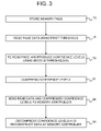
- FIG. 3 is a flow chart that schematically illustrates a method for data readout from analog memory cells 32 , in accordance with an embodiment of the present invention.
- the method begins with memory controller 40 storing a page of data in memory device 24 , at a storage step 70 .
- ECC unit 47 in controller 40 encodes the data with an ECC, and the encoded data is transferred to the memory device.
- R/W unit 36 writes storage values representing the encoded data into a group of memory cells 32 .
- the memory controller requests the memory device to retrieve the data page in question.
- R/W unit 36 reads the page, at a reading step 74 .
- the R/W unit reads the page by comparing the storage values of the memory cells in the group to read threshold 52 (see FIG. 2 ). The comparison results produce the B 1 data values shown in FIG. 2 .
- the R/W unit re-reads the page to produce respective estimated confidence levels of the storage values, at a re-reading step 78 .
- the R/W unit re-reads the page using read thresholds 60 , to produce the B 2 value shown in FIG. 2 .
- Compression module 45 in R/W unit 36 compresses the estimated confidence levels, at a compression step 82 .
- Any suitable compression scheme such as the example compression schemes described above, can be used.
- the R/W unit transfers the read data values and the compressed confidence levels to the memory controller, at a transfer step 86 .
- decompression module 46 decompresses the compressed confidence levels received over the interface from the memory device, and reconstructs the data page, at a reconstruction step 90 .
- ECC unit 47 decodes the ECC of the page using the decompressed confidence levels.
- memory controller 40 may decode the ECC by operating on soft metrics (e.g., LLRs), which are computed based on the confidence levels transferred from the memory device.
- soft metrics e.g., LLRs
- the memory controller refines the soft metrics in an iterative manner by obtaining additional confidence level information regarding the storage values of the memory cells.
- the memory controller initially attempts to decode the ECC based on the read data values (i.e., using hard metrics), and refines the metrics iteratively until the ECC is decoded successfully.
- FIG. 4 is a flow chart that schematically illustrates an iterative process for data readout from memory cells 32 , in accordance with an embodiment of the present invention.
- the method begins with memory controller 40 reading the data values of a certain memory page, at a page readout step 100 .
- ECC unit 47 attempts to decode the ECC, at a decoding step 104 .
- the ECC unit decodes the ECC using soft metrics, which are further refined in each iteration. In the first iteration, the metrics comprise the read data values, i.e., hard metrics.
- Controller 40 checks whether the ECC is decoded successfully, at a checking step 108 . If successful, the memory controller outputs the retrieved data page, and the method terminates, at a termination step 112 . If, on the other hand, the ECC decoding attempt failed, the memory controller refines the soft metrics based on additional confidence level information regarding the read storage values, at a refinement step 114 .
- the additional confidence level information is obtained from memory device 24 concurrently with the ECC decoding attempt.
- the refined information may comprise, for example, an additional confidence level bit for each storage value.
- the additional confidence level information is typically obtained by re-reading the page using one or more read thresholds, which are different from the thresholds used in previous iterations.
- R/W unit 36 in memory device 24 obtains and compresses the additional confidence level information, at a re-reading and compression step 116 .
- Memory controller 40 decompresses the additional confidence level information, at an additional decompression step 120 .
- the memory controller then combines the confidence level information obtained in the current iteration with the previously-existing confidence level information, at a combining step 114 .
- the new and existing confidence level information is combined so as to refine the soft metrics of the storage values.
- the method then loops back to step 100 above, in which ECC module 47 attempts to decode the ECC using the refined soft metrics.
- the R/W unit may obtain and provide refined confidence level information only for storage values that were identified in previous iterations as having low confidence levels. This technique further reduces the volume of confidence level information transferred to the memory controller. Techniques of this sort are addressed, for example, in U.S. Provisional Patent Applications 61/052,276 and 61/053,031, cited above.
- the memory controller may apply different policies regarding refinement the confidence levels at different stages of the memory device's life cycle.
- the distortion in memory cells 32 is relatively low, and ECC decoding using hard metrics is likely to succeed.
- the distortion level in cells 32 grows, so that hard decoding may be unlikely to succeed.
- the memory device initially begins to operate using the method of FIG. 4 above.
- the memory device may switch to a different mode of operation, in which it requests the memory device to produce soft metrics to begin with, without initially attempting hard decoding.
- a certain memory cell is read using multiple different read thresholds. It is typically desirable to reduce the sense time involved in these multiple reading operation.
- a possible technique for rapidly reading a given memory cell multiple times using multiple read thresholds is described in PCT International Publication WO 2008/053473, whose disclosure is incorporated herein by reference.
- the confidence levels are obtained by re-reading the memory cells using different read thresholds.
- the memory device may determine the confidence levels of the storage values using any other suitable method. All of the techniques described below can be carried out as part of the method of FIG. 3 above, or as part of the iterative method of FIG. 4 above. When carrying out the method of FIG. 4 , calculation of the refined confidence level information can be performed either after or in semi-parallel with transferring the initial read results and decoding the ECC.
- the memory device may initially read the memory cells using a relatively fast read operation, which has a certain accuracy level (e.g., a read operation having a short sense time).
- the memory device can re-read the memory cells using a slower but more accurate read operation (e.g., by using a longer sense time).
- the results of the first and second read operations will typically differ in only a small number of cells. Therefore, the differences between the respective read results of the two read operations can be regarded as confidence levels and sent to the controller using any of the methods described herein.
- the second read operation is invoked only when the memory controller fails to decode the ECC based on the results of the first read operation. This technique may be particularly suitable for memory devices in which the busy period of the read operation is long.
- the memory device may re-read the memory cells several times (e.g., three times) using the same read thresholds and determine the confidence levels from the multiple read results, e.g., by performing a majority vote.
- This scheme can be applied iteratively. For example, the memory device can read the memory cells once and transfer the results to the memory controller. Then, the memory device can re-read the memory cells twice more, perform a majority vote and regard any corrections (i.e., discrepancies between the initial read results and the results of the majority vote) as low confidence levels that are to be transferred to the memory controller.
- the additional read operations may be invoked conditionally—upon failure to decode the ECC based on the initial read results.
Abstract
Description
-
- a plurality of analog memory cells; and
- circuitry, which is coupled to store data in a group of the analog memory cells by writing respective input storage values to the memory cells in the group, to read respective output storage values from the analog memory cells in the group after storing the data, to estimate respective confidence levels of the output storage values, to compress the confidence levels, and to transfer the output storage values and the compressed confidence levels from the memory cells over an interface; and
| Information | ||||
| Bus cycle # | SoftIndication | on bus | ||
| . . . | . . . | . . . | ||
| . . . | . . . | . . . | ||
| M | “1” | VAL (N) | ||
| M + 1 | “1” | VAL (N + 1) | ||
| M + 2 | “0” | VAL (N + 2) | ||
| M + 3 | “0” | IND (VAL (N + 2) ) | ||
| M + 4 | “1” | VAL (N + 3) | ||
| . . . | . . . | . . . | ||
| . . . | . . . | . . . | ||
| . . . | . . . | . . . | ||
| Information | |||
| Bus cycle # | on |
||
| 1 | VAL (1) | ||
| 2 | VAL (2) | ||
| . . . | . . . | ||
| N = 4224 | VAL (N) | ||
| N + 1 | COMP (1) | ||
| N + 2 | COMP (2) | ||
| . . . | . . . | ||
| N + M | COMP (M) | ||
Claims (34)
Priority Applications (4)
| Application Number | Priority Date | Filing Date | Title |
|---|---|---|---|
| US12/397,368 US8230300B2 (en) | 2008-03-07 | 2009-03-04 | Efficient readout from analog memory cells using data compression |
| US13/526,859 US9229861B2 (en) | 2008-03-07 | 2012-06-19 | Efficient readout from analog memory cells using data compression |
| US14/987,324 US9671972B2 (en) | 2008-03-07 | 2016-01-04 | Efficient readout from memory cells using data compression |
| US15/602,444 US10157013B2 (en) | 2008-03-07 | 2017-05-23 | Efficient readout from memory cells using data compression |
Applications Claiming Priority (4)
| Application Number | Priority Date | Filing Date | Title |
|---|---|---|---|
| US3451108P | 2008-03-07 | 2008-03-07 | |
| US5227608P | 2008-05-12 | 2008-05-12 | |
| US5303108P | 2008-05-14 | 2008-05-14 | |
| US12/397,368 US8230300B2 (en) | 2008-03-07 | 2009-03-04 | Efficient readout from analog memory cells using data compression |
Related Child Applications (1)
| Application Number | Title | Priority Date | Filing Date |
|---|---|---|---|
| US13/526,859 Continuation US9229861B2 (en) | 2008-03-07 | 2012-06-19 | Efficient readout from analog memory cells using data compression |
Publications (2)
| Publication Number | Publication Date |
|---|---|
| US20090228761A1 US20090228761A1 (en) | 2009-09-10 |
| US8230300B2 true US8230300B2 (en) | 2012-07-24 |
Family
ID=41054861
Family Applications (4)
| Application Number | Title | Priority Date | Filing Date |
|---|---|---|---|
| US12/397,368 Active 2031-02-22 US8230300B2 (en) | 2008-03-07 | 2009-03-04 | Efficient readout from analog memory cells using data compression |
| US13/526,859 Active 2031-01-11 US9229861B2 (en) | 2008-03-07 | 2012-06-19 | Efficient readout from analog memory cells using data compression |
| US14/987,324 Active US9671972B2 (en) | 2008-03-07 | 2016-01-04 | Efficient readout from memory cells using data compression |
| US15/602,444 Active US10157013B2 (en) | 2008-03-07 | 2017-05-23 | Efficient readout from memory cells using data compression |
Family Applications After (3)
| Application Number | Title | Priority Date | Filing Date |
|---|---|---|---|
| US13/526,859 Active 2031-01-11 US9229861B2 (en) | 2008-03-07 | 2012-06-19 | Efficient readout from analog memory cells using data compression |
| US14/987,324 Active US9671972B2 (en) | 2008-03-07 | 2016-01-04 | Efficient readout from memory cells using data compression |
| US15/602,444 Active US10157013B2 (en) | 2008-03-07 | 2017-05-23 | Efficient readout from memory cells using data compression |
Country Status (1)
| Country | Link |
|---|---|
| US (4) | US8230300B2 (en) |
Cited By (14)
| Publication number | Priority date | Publication date | Assignee | Title |
|---|---|---|---|---|
| US20110138254A1 (en) * | 2009-12-08 | 2011-06-09 | Tsung-Chieh Yang | Method for reducing uncorrectable errors of a memory device regarding error correction code, and associated memory device and controller thereof |
| US20110320913A1 (en) * | 2010-06-28 | 2011-12-29 | Henry Stracovsky | Reliability support in memory systems without error correcting code support |
| US20130063997A1 (en) * | 2011-09-14 | 2013-03-14 | Ariel Maislos | High-Resolution Readout of Analog Memory Cells |
| US20130297989A1 (en) * | 2008-03-18 | 2013-11-07 | Apple Inc. | Memory Device Readout Using Multiple Sense Times |
| US8787057B2 (en) | 2012-08-15 | 2014-07-22 | Apple Inc. | Fast analog memory cell readout using modified bit-line charging configurations |
| US9058890B2 (en) | 2007-02-27 | 2015-06-16 | Samsung Electronics Co., Ltd. | Over-sampling read operation for a flash memory device |
| US9159440B2 (en) | 2010-03-29 | 2015-10-13 | Samsung Electronics Co., Ltd. | Read method for nonvolatile memory device, and data storage system using the same |
| US9224489B2 (en) | 2010-02-08 | 2015-12-29 | Samsung Electronics Co., Ltd. | Flash memory devices having multi-bit memory cells therein with improved read reliability |
| US9256493B2 (en) | 2011-12-28 | 2016-02-09 | Intel Corporation | Memory module architecture |
| US9858994B2 (en) * | 2015-06-18 | 2018-01-02 | Samsung Electronics Co., Ltd. | Memory system with MLC memory cells and partial page compression or reduction |
| US20180151222A1 (en) * | 2012-04-26 | 2018-05-31 | Hgst Technologies Santa Ana, Inc. | Soft information module |
| US20210011654A1 (en) * | 2018-03-29 | 2021-01-14 | Samsung Electronics Co., Ltd. | Method for processing data and electronic device supporting same |
| US11556416B2 (en) | 2021-05-05 | 2023-01-17 | Apple Inc. | Controlling memory readout reliability and throughput by adjusting distance between read thresholds |
| US11847342B2 (en) | 2021-07-28 | 2023-12-19 | Apple Inc. | Efficient transfer of hard data and confidence levels in reading a nonvolatile memory |
Families Citing this family (226)
| Publication number | Priority date | Publication date | Assignee | Title |
|---|---|---|---|---|
| CN103258572B (en) | 2006-05-12 | 2016-12-07 | 苹果公司 | Distortion estimation in storage device and elimination |
| WO2008053472A2 (en) | 2006-10-30 | 2008-05-08 | Anobit Technologies Ltd. | Reading memory cells using multiple thresholds |
| US7751240B2 (en) | 2007-01-24 | 2010-07-06 | Anobit Technologies Ltd. | Memory device with negative thresholds |
| CN101715595A (en) | 2007-03-12 | 2010-05-26 | 爱诺彼得技术有限责任公司 | Adaptive estimation of memory cell read thresholds |
| WO2008139441A2 (en) | 2007-05-12 | 2008-11-20 | Anobit Technologies Ltd. | Memory device with internal signal processing unit |
| US8174905B2 (en) | 2007-09-19 | 2012-05-08 | Anobit Technologies Ltd. | Programming orders for reducing distortion in arrays of multi-level analog memory cells |
| WO2009095902A2 (en) | 2008-01-31 | 2009-08-06 | Densbits Technologies Ltd. | Systems and methods for handling immediate data errors in flash memory |
| US8650352B2 (en) | 2007-09-20 | 2014-02-11 | Densbits Technologies Ltd. | Systems and methods for determining logical values of coupled flash memory cells |
| WO2009050703A2 (en) | 2007-10-19 | 2009-04-23 | Anobit Technologies | Data storage in analog memory cell arrays having erase failures |
| US8694715B2 (en) | 2007-10-22 | 2014-04-08 | Densbits Technologies Ltd. | Methods for adaptively programming flash memory devices and flash memory systems incorporating same |
| WO2009053962A2 (en) * | 2007-10-22 | 2009-04-30 | Densbits Technologies Ltd. | Systems and methods for averaging error rates in non-volatile devices and storage systems |
| US8443242B2 (en) * | 2007-10-25 | 2013-05-14 | Densbits Technologies Ltd. | Systems and methods for multiple coding rates in flash devices |
| WO2009063450A2 (en) | 2007-11-13 | 2009-05-22 | Anobit Technologies | Optimized selection of memory units in multi-unit memory devices |
| WO2009072104A2 (en) | 2007-12-05 | 2009-06-11 | Densbits Technologies Ltd. | Flash memory device with physical cell value deterioration accommodation and methods useful in conjunction therewith |
| US8607128B2 (en) | 2007-12-05 | 2013-12-10 | Densbits Technologies Ltd. | Low power chien-search based BCH/RS decoding system for flash memory, mobile communications devices and other applications |
| WO2009072103A2 (en) * | 2007-12-05 | 2009-06-11 | Densbits Technologies Ltd. | Flash memory apparatus and methods using a plurality of decoding stages including optional use of concatenated bch codes and/or designation of 'first below' cells |
| US8359516B2 (en) * | 2007-12-12 | 2013-01-22 | Densbits Technologies Ltd. | Systems and methods for error correction and decoding on multi-level physical media |
| US8276051B2 (en) * | 2007-12-12 | 2012-09-25 | Densbits Technologies Ltd. | Chien-search system employing a clock-gating scheme to save power for error correction decoder and other applications |
| US8327246B2 (en) * | 2007-12-18 | 2012-12-04 | Densbits Technologies Ltd. | Apparatus for coding at a plurality of rates in multi-level flash memory systems, and methods useful in conjunction therewith |
| US7934052B2 (en) | 2007-12-27 | 2011-04-26 | Pliant Technology, Inc. | System and method for performing host initiated mass storage commands using a hierarchy of data structures |
| US8230300B2 (en) * | 2008-03-07 | 2012-07-24 | Apple Inc. | Efficient readout from analog memory cells using data compression |
| US8400858B2 (en) | 2008-03-18 | 2013-03-19 | Apple Inc. | Memory device with reduced sense time readout |
| US8059457B2 (en) | 2008-03-18 | 2011-11-15 | Anobit Technologies Ltd. | Memory device with multiple-accuracy read commands |
| WO2009118720A2 (en) | 2008-03-25 | 2009-10-01 | Densbits Technologies Ltd. | Apparatus and methods for hardware-efficient unbiased rounding |
| US7924613B1 (en) | 2008-08-05 | 2011-04-12 | Anobit Technologies Ltd. | Data storage in analog memory cells with protection against programming interruption |
| US7995388B1 (en) | 2008-08-05 | 2011-08-09 | Anobit Technologies Ltd. | Data storage using modified voltages |
| US8332725B2 (en) * | 2008-08-20 | 2012-12-11 | Densbits Technologies Ltd. | Reprogramming non volatile memory portions |
| US8169825B1 (en) | 2008-09-02 | 2012-05-01 | Anobit Technologies Ltd. | Reliable data storage in analog memory cells subjected to long retention periods |
| US8949684B1 (en) | 2008-09-02 | 2015-02-03 | Apple Inc. | Segmented data storage |
| US8482978B1 (en) | 2008-09-14 | 2013-07-09 | Apple Inc. | Estimation of memory cell read thresholds by sampling inside programming level distribution intervals |
| US8000135B1 (en) | 2008-09-14 | 2011-08-16 | Anobit Technologies Ltd. | Estimation of memory cell read thresholds by sampling inside programming level distribution intervals |
| US8239734B1 (en) | 2008-10-15 | 2012-08-07 | Apple Inc. | Efficient data storage in storage device arrays |
| US8261159B1 (en) | 2008-10-30 | 2012-09-04 | Apple, Inc. | Data scrambling schemes for memory devices |
| US8208304B2 (en) | 2008-11-16 | 2012-06-26 | Anobit Technologies Ltd. | Storage at M bits/cell density in N bits/cell analog memory cell devices, M>N |
| US8397131B1 (en) | 2008-12-31 | 2013-03-12 | Apple Inc. | Efficient readout schemes for analog memory cell devices |
| US8248831B2 (en) | 2008-12-31 | 2012-08-21 | Apple Inc. | Rejuvenation of analog memory cells |
| US8924661B1 (en) | 2009-01-18 | 2014-12-30 | Apple Inc. | Memory system including a controller and processors associated with memory devices |
| US8228701B2 (en) | 2009-03-01 | 2012-07-24 | Apple Inc. | Selective activation of programming schemes in analog memory cell arrays |
| US8266503B2 (en) | 2009-03-13 | 2012-09-11 | Fusion-Io | Apparatus, system, and method for using multi-level cell storage in a single-level cell mode |
| US8261158B2 (en) | 2009-03-13 | 2012-09-04 | Fusion-Io, Inc. | Apparatus, system, and method for using multi-level cell solid-state storage as single level cell solid-state storage |
| US8832354B2 (en) | 2009-03-25 | 2014-09-09 | Apple Inc. | Use of host system resources by memory controller |
| US8259506B1 (en) | 2009-03-25 | 2012-09-04 | Apple Inc. | Database of memory read thresholds |
| US8819385B2 (en) * | 2009-04-06 | 2014-08-26 | Densbits Technologies Ltd. | Device and method for managing a flash memory |
| US8458574B2 (en) | 2009-04-06 | 2013-06-04 | Densbits Technologies Ltd. | Compact chien-search based decoding apparatus and method |
| US8238157B1 (en) | 2009-04-12 | 2012-08-07 | Apple Inc. | Selective re-programming of analog memory cells |
| US8566510B2 (en) * | 2009-05-12 | 2013-10-22 | Densbits Technologies Ltd. | Systems and method for flash memory management |
| US8479080B1 (en) | 2009-07-12 | 2013-07-02 | Apple Inc. | Adaptive over-provisioning in memory systems |
| US8868821B2 (en) * | 2009-08-26 | 2014-10-21 | Densbits Technologies Ltd. | Systems and methods for pre-equalization and code design for a flash memory |
| US8995197B1 (en) | 2009-08-26 | 2015-03-31 | Densbits Technologies Ltd. | System and methods for dynamic erase and program control for flash memory device memories |
| US9330767B1 (en) | 2009-08-26 | 2016-05-03 | Avago Technologies General Ip (Singapore) Pte. Ltd. | Flash memory module and method for programming a page of flash memory cells |
| US8305812B2 (en) | 2009-08-26 | 2012-11-06 | Densbits Technologies Ltd. | Flash memory module and method for programming a page of flash memory cells |
| US8495465B1 (en) | 2009-10-15 | 2013-07-23 | Apple Inc. | Error correction coding over multiple memory pages |
| US8730729B2 (en) | 2009-10-15 | 2014-05-20 | Densbits Technologies Ltd. | Systems and methods for averaging error rates in non-volatile devices and storage systems |
| US8724387B2 (en) * | 2009-10-22 | 2014-05-13 | Densbits Technologies Ltd. | Method, system, and computer readable medium for reading and programming flash memory cells using multiple bias voltages |
| US8626988B2 (en) | 2009-11-19 | 2014-01-07 | Densbits Technologies Ltd. | System and method for uncoded bit error rate equalization via interleaving |
| US8677054B1 (en) | 2009-12-16 | 2014-03-18 | Apple Inc. | Memory management schemes for non-volatile memory devices |
| US9037777B2 (en) | 2009-12-22 | 2015-05-19 | Densbits Technologies Ltd. | Device, system, and method for reducing program/read disturb in flash arrays |
| US8607124B2 (en) | 2009-12-24 | 2013-12-10 | Densbits Technologies Ltd. | System and method for setting a flash memory cell read threshold |
| US8694814B1 (en) | 2010-01-10 | 2014-04-08 | Apple Inc. | Reuse of host hibernation storage space by memory controller |
| US8572311B1 (en) | 2010-01-11 | 2013-10-29 | Apple Inc. | Redundant data storage in multi-die memory systems |
| US8661184B2 (en) | 2010-01-27 | 2014-02-25 | Fusion-Io, Inc. | Managing non-volatile media |
| US8380915B2 (en) | 2010-01-27 | 2013-02-19 | Fusion-Io, Inc. | Apparatus, system, and method for managing solid-state storage media |
| US8315092B2 (en) | 2010-01-27 | 2012-11-20 | Fusion-Io, Inc. | Apparatus, system, and method for determining a read voltage threshold for solid-state storage media |
| US8854882B2 (en) | 2010-01-27 | 2014-10-07 | Intelligent Intellectual Property Holdings 2 Llc | Configuring storage cells |
| US8700970B2 (en) | 2010-02-28 | 2014-04-15 | Densbits Technologies Ltd. | System and method for multi-dimensional decoding |
| US9245653B2 (en) | 2010-03-15 | 2016-01-26 | Intelligent Intellectual Property Holdings 2 Llc | Reduced level cell mode for non-volatile memory |
| US8527840B2 (en) | 2010-04-06 | 2013-09-03 | Densbits Technologies Ltd. | System and method for restoring damaged data programmed on a flash device |
| US8516274B2 (en) | 2010-04-06 | 2013-08-20 | Densbits Technologies Ltd. | Method, system and medium for analog encryption in a flash memory |
| US8745317B2 (en) | 2010-04-07 | 2014-06-03 | Densbits Technologies Ltd. | System and method for storing information in a multi-level cell memory |
| US9021177B2 (en) | 2010-04-29 | 2015-04-28 | Densbits Technologies Ltd. | System and method for allocating and using spare blocks in a flash memory |
| US8694853B1 (en) | 2010-05-04 | 2014-04-08 | Apple Inc. | Read commands for reading interfering memory cells |
| US8572423B1 (en) | 2010-06-22 | 2013-10-29 | Apple Inc. | Reducing peak current in memory systems |
| US8539311B2 (en) | 2010-07-01 | 2013-09-17 | Densbits Technologies Ltd. | System and method for data recovery in multi-level cell memories |
| US8621321B2 (en) | 2010-07-01 | 2013-12-31 | Densbits Technologies Ltd. | System and method for multi-dimensional encoding and decoding |
| US20120008414A1 (en) | 2010-07-06 | 2012-01-12 | Michael Katz | Systems and methods for storing, retrieving, and adjusting read thresholds in flash memory storage system |
| US8595591B1 (en) | 2010-07-11 | 2013-11-26 | Apple Inc. | Interference-aware assignment of programming levels in analog memory cells |
| TWI455144B (en) * | 2010-07-22 | 2014-10-01 | Silicon Motion Inc | Controlling methods and controllers utilized in flash memory device |
| US9104580B1 (en) | 2010-07-27 | 2015-08-11 | Apple Inc. | Cache memory for hybrid disk drives |
| US8767459B1 (en) | 2010-07-31 | 2014-07-01 | Apple Inc. | Data storage in analog memory cells across word lines using a non-integer number of bits per cell |
| US8856475B1 (en) | 2010-08-01 | 2014-10-07 | Apple Inc. | Efficient selection of memory blocks for compaction |
| US8694854B1 (en) | 2010-08-17 | 2014-04-08 | Apple Inc. | Read threshold setting based on soft readout statistics |
| US8964464B2 (en) | 2010-08-24 | 2015-02-24 | Densbits Technologies Ltd. | System and method for accelerated sampling |
| US8508995B2 (en) | 2010-09-15 | 2013-08-13 | Densbits Technologies Ltd. | System and method for adjusting read voltage thresholds in memories |
| US9021181B1 (en) | 2010-09-27 | 2015-04-28 | Apple Inc. | Memory management for unifying memory cell conditions by using maximum time intervals |
| US9063878B2 (en) | 2010-11-03 | 2015-06-23 | Densbits Technologies Ltd. | Method, system and computer readable medium for copy back |
| US8850100B2 (en) | 2010-12-07 | 2014-09-30 | Densbits Technologies Ltd. | Interleaving codeword portions between multiple planes and/or dies of a flash memory device |
| US9898361B2 (en) | 2011-01-04 | 2018-02-20 | Seagate Technology Llc | Multi-tier detection and decoding in flash memories |
| US9292377B2 (en) | 2011-01-04 | 2016-03-22 | Seagate Technology Llc | Detection and decoding in flash memories using correlation of neighboring bits and probability based reliability values |
| US8909851B2 (en) | 2011-02-08 | 2014-12-09 | SMART Storage Systems, Inc. | Storage control system with change logging mechanism and method of operation thereof |
| US10079068B2 (en) | 2011-02-23 | 2018-09-18 | Avago Technologies General Ip (Singapore) Pte. Ltd. | Devices and method for wear estimation based memory management |
| US8693258B2 (en) | 2011-03-17 | 2014-04-08 | Densbits Technologies Ltd. | Obtaining soft information using a hard interface |
| US8935466B2 (en) | 2011-03-28 | 2015-01-13 | SMART Storage Systems, Inc. | Data storage system with non-volatile memory and method of operation thereof |
| CN102122959B (en) * | 2011-03-29 | 2013-12-04 | 西安交通大学 | Data compression device for improving main memory reliability of computer, and method thereof |
| US8990665B1 (en) | 2011-04-06 | 2015-03-24 | Densbits Technologies Ltd. | System, method and computer program product for joint search of a read threshold and soft decoding |
| US9195592B1 (en) | 2011-05-12 | 2015-11-24 | Densbits Technologies Ltd. | Advanced management of a non-volatile memory |
| US9501392B1 (en) | 2011-05-12 | 2016-11-22 | Avago Technologies General Ip (Singapore) Pte. Ltd. | Management of a non-volatile memory module |
| US8996790B1 (en) | 2011-05-12 | 2015-03-31 | Densbits Technologies Ltd. | System and method for flash memory management |
| US9110785B1 (en) | 2011-05-12 | 2015-08-18 | Densbits Technologies Ltd. | Ordered merge of data sectors that belong to memory space portions |
| US9372792B1 (en) | 2011-05-12 | 2016-06-21 | Avago Technologies General Ip (Singapore) Pte. Ltd. | Advanced management of a non-volatile memory |
| US9396106B2 (en) | 2011-05-12 | 2016-07-19 | Avago Technologies General Ip (Singapore) Pte. Ltd. | Advanced management of a non-volatile memory |
| US8667211B2 (en) | 2011-06-01 | 2014-03-04 | Densbits Technologies Ltd. | System and method for managing a non-volatile memory |
| US8910020B2 (en) | 2011-06-19 | 2014-12-09 | Sandisk Enterprise Ip Llc | Intelligent bit recovery for flash memory |
| US8909982B2 (en) | 2011-06-19 | 2014-12-09 | Sandisk Enterprise Ip Llc | System and method for detecting copyback programming problems |
| US8588003B1 (en) | 2011-08-01 | 2013-11-19 | Densbits Technologies Ltd. | System, method and computer program product for programming and for recovering from a power failure |
| US9098399B2 (en) | 2011-08-31 | 2015-08-04 | SMART Storage Systems, Inc. | Electronic system with storage management mechanism and method of operation thereof |
| US9063844B2 (en) | 2011-09-02 | 2015-06-23 | SMART Storage Systems, Inc. | Non-volatile memory management system with time measure mechanism and method of operation thereof |
| US9021231B2 (en) | 2011-09-02 | 2015-04-28 | SMART Storage Systems, Inc. | Storage control system with write amplification control mechanism and method of operation thereof |
| US9021319B2 (en) | 2011-09-02 | 2015-04-28 | SMART Storage Systems, Inc. | Non-volatile memory management system with load leveling and method of operation thereof |
| US8553468B2 (en) | 2011-09-21 | 2013-10-08 | Densbits Technologies Ltd. | System and method for managing erase operations in a non-volatile memory |
| US9058289B2 (en) | 2011-11-07 | 2015-06-16 | Sandisk Enterprise Ip Llc | Soft information generation for memory systems |
| US8954822B2 (en) | 2011-11-18 | 2015-02-10 | Sandisk Enterprise Ip Llc | Data encoder and decoder using memory-specific parity-check matrix |
| US8924815B2 (en) | 2011-11-18 | 2014-12-30 | Sandisk Enterprise Ip Llc | Systems, methods and devices for decoding codewords having multiple parity segments |
| US9048876B2 (en) | 2011-11-18 | 2015-06-02 | Sandisk Enterprise Ip Llc | Systems, methods and devices for multi-tiered error correction |
| US9239781B2 (en) | 2012-02-07 | 2016-01-19 | SMART Storage Systems, Inc. | Storage control system with erase block mechanism and method of operation thereof |
| US8996788B2 (en) | 2012-02-09 | 2015-03-31 | Densbits Technologies Ltd. | Configurable flash interface |
| US8947941B2 (en) | 2012-02-09 | 2015-02-03 | Densbits Technologies Ltd. | State responsive operations relating to flash memory cells |
| JP5768022B2 (en) | 2012-03-19 | 2015-08-26 | 株式会社東芝 | Memory controller, storage device, error correction device, and error correction method |
| CN104205235B (en) * | 2012-03-29 | 2017-08-08 | 英特尔公司 | Method and apparatus for handling the state confidence data retrieved from nonvolatile memory array |
| US8996793B1 (en) | 2012-04-24 | 2015-03-31 | Densbits Technologies Ltd. | System, method and computer readable medium for generating soft information |
| TW201346922A (en) * | 2012-05-14 | 2013-11-16 | Toshiba Kk | Memory controller, storage device and error correction method |
| US8838937B1 (en) | 2012-05-23 | 2014-09-16 | Densbits Technologies Ltd. | Methods, systems and computer readable medium for writing and reading data |
| US8879325B1 (en) | 2012-05-30 | 2014-11-04 | Densbits Technologies Ltd. | System, method and computer program product for processing read threshold information and for reading a flash memory module |
| US8949689B2 (en) | 2012-06-11 | 2015-02-03 | SMART Storage Systems, Inc. | Storage control system with data management mechanism and method of operation thereof |
| US8804415B2 (en) | 2012-06-19 | 2014-08-12 | Fusion-Io, Inc. | Adaptive voltage range management in non-volatile memory |
| US9699263B1 (en) | 2012-08-17 | 2017-07-04 | Sandisk Technologies Llc. | Automatic read and write acceleration of data accessed by virtual machines |
| US9921954B1 (en) | 2012-08-27 | 2018-03-20 | Avago Technologies General Ip (Singapore) Pte. Ltd. | Method and system for split flash memory management between host and storage controller |
| US9368225B1 (en) | 2012-11-21 | 2016-06-14 | Avago Technologies General Ip (Singapore) Pte. Ltd. | Determining read thresholds based upon read error direction statistics |
| US9671962B2 (en) | 2012-11-30 | 2017-06-06 | Sandisk Technologies Llc | Storage control system with data management mechanism of parity and method of operation thereof |
| US9501398B2 (en) | 2012-12-26 | 2016-11-22 | Sandisk Technologies Llc | Persistent storage device with NVRAM for staging writes |
| US9141532B2 (en) * | 2012-12-26 | 2015-09-22 | Western Digital Technologies, Inc. | Dynamic overprovisioning for data storage systems |
| US9612948B2 (en) | 2012-12-27 | 2017-04-04 | Sandisk Technologies Llc | Reads and writes between a contiguous data block and noncontiguous sets of logical address blocks in a persistent storage device |
| US9239751B1 (en) | 2012-12-27 | 2016-01-19 | Sandisk Enterprise Ip Llc | Compressing data from multiple reads for error control management in memory systems |
| US9454420B1 (en) | 2012-12-31 | 2016-09-27 | Sandisk Technologies Llc | Method and system of reading threshold voltage equalization |
| US9069659B1 (en) | 2013-01-03 | 2015-06-30 | Densbits Technologies Ltd. | Read threshold determination using reference read threshold |
| US9123445B2 (en) | 2013-01-22 | 2015-09-01 | SMART Storage Systems, Inc. | Storage control system with data management mechanism and method of operation thereof |
| US9214965B2 (en) * | 2013-02-20 | 2015-12-15 | Sandisk Enterprise Ip Llc | Method and system for improving data integrity in non-volatile storage |
| US9329928B2 (en) * | 2013-02-20 | 2016-05-03 | Sandisk Enterprise IP LLC. | Bandwidth optimization in a non-volatile memory system |
| US9183137B2 (en) | 2013-02-27 | 2015-11-10 | SMART Storage Systems, Inc. | Storage control system with data management mechanism and method of operation thereof |
| US9470720B2 (en) | 2013-03-08 | 2016-10-18 | Sandisk Technologies Llc | Test system with localized heating and method of manufacture thereof |
| US9136877B1 (en) | 2013-03-15 | 2015-09-15 | Sandisk Enterprise Ip Llc | Syndrome layered decoding for LDPC codes |
| US9367246B2 (en) | 2013-03-15 | 2016-06-14 | Sandisk Technologies Inc. | Performance optimization of data transfer for soft information generation |
| US9092350B1 (en) | 2013-03-15 | 2015-07-28 | Sandisk Enterprise Ip Llc | Detection and handling of unbalanced errors in interleaved codewords |
| US9236886B1 (en) | 2013-03-15 | 2016-01-12 | Sandisk Enterprise Ip Llc | Universal and reconfigurable QC-LDPC encoder |
| US9244763B1 (en) | 2013-03-15 | 2016-01-26 | Sandisk Enterprise Ip Llc | System and method for updating a reading threshold voltage based on symbol transition information |
| JP5851441B2 (en) * | 2013-03-25 | 2016-02-03 | 株式会社東芝 | NAND flash memory controller |
| US9043780B2 (en) | 2013-03-27 | 2015-05-26 | SMART Storage Systems, Inc. | Electronic system with system modification control mechanism and method of operation thereof |
| US10049037B2 (en) | 2013-04-05 | 2018-08-14 | Sandisk Enterprise Ip Llc | Data management in a storage system |
| US9170941B2 (en) | 2013-04-05 | 2015-10-27 | Sandisk Enterprises IP LLC | Data hardening in a storage system |
| US9543025B2 (en) | 2013-04-11 | 2017-01-10 | Sandisk Technologies Llc | Storage control system with power-off time estimation mechanism and method of operation thereof |
| US10546648B2 (en) | 2013-04-12 | 2020-01-28 | Sandisk Technologies Llc | Storage control system with data management mechanism and method of operation thereof |
| US9136876B1 (en) | 2013-06-13 | 2015-09-15 | Densbits Technologies Ltd. | Size limited multi-dimensional decoding |
| US9898056B2 (en) | 2013-06-19 | 2018-02-20 | Sandisk Technologies Llc | Electronic assembly with thermal channel and method of manufacture thereof |
| US9313874B2 (en) | 2013-06-19 | 2016-04-12 | SMART Storage Systems, Inc. | Electronic system with heat extraction and method of manufacture thereof |
| US9244519B1 (en) | 2013-06-25 | 2016-01-26 | Smart Storage Systems. Inc. | Storage system with data transfer rate adjustment for power throttling |
| US9367353B1 (en) | 2013-06-25 | 2016-06-14 | Sandisk Technologies Inc. | Storage control system with power throttling mechanism and method of operation thereof |
| US9384126B1 (en) | 2013-07-25 | 2016-07-05 | Sandisk Technologies Inc. | Methods and systems to avoid false negative results in bloom filters implemented in non-volatile data storage systems |
| US9043517B1 (en) | 2013-07-25 | 2015-05-26 | Sandisk Enterprise Ip Llc | Multipass programming in buffers implemented in non-volatile data storage systems |
| US9524235B1 (en) | 2013-07-25 | 2016-12-20 | Sandisk Technologies Llc | Local hash value generation in non-volatile data storage systems |
| US9146850B2 (en) | 2013-08-01 | 2015-09-29 | SMART Storage Systems, Inc. | Data storage system with dynamic read threshold mechanism and method of operation thereof |
| US9361222B2 (en) | 2013-08-07 | 2016-06-07 | SMART Storage Systems, Inc. | Electronic system with storage drive life estimation mechanism and method of operation thereof |
| US9431113B2 (en) | 2013-08-07 | 2016-08-30 | Sandisk Technologies Llc | Data storage system with dynamic erase block grouping mechanism and method of operation thereof |
| US9448946B2 (en) | 2013-08-07 | 2016-09-20 | Sandisk Technologies Llc | Data storage system with stale data mechanism and method of operation thereof |
| US9639463B1 (en) | 2013-08-26 | 2017-05-02 | Sandisk Technologies Llc | Heuristic aware garbage collection scheme in storage systems |
| US9361221B1 (en) | 2013-08-26 | 2016-06-07 | Sandisk Technologies Inc. | Write amplification reduction through reliable writes during garbage collection |
| US9519577B2 (en) | 2013-09-03 | 2016-12-13 | Sandisk Technologies Llc | Method and system for migrating data between flash memory devices |
| US9442670B2 (en) | 2013-09-03 | 2016-09-13 | Sandisk Technologies Llc | Method and system for rebalancing data stored in flash memory devices |
| US9158349B2 (en) | 2013-10-04 | 2015-10-13 | Sandisk Enterprise Ip Llc | System and method for heat dissipation |
| US9413491B1 (en) | 2013-10-08 | 2016-08-09 | Avago Technologies General Ip (Singapore) Pte. Ltd. | System and method for multiple dimension decoding and encoding a message |
| US9786388B1 (en) | 2013-10-09 | 2017-10-10 | Avago Technologies General Ip (Singapore) Pte. Ltd. | Detecting and managing bad columns |
| US9397706B1 (en) | 2013-10-09 | 2016-07-19 | Avago Technologies General Ip (Singapore) Pte. Ltd. | System and method for irregular multiple dimension decoding and encoding |
| US9348694B1 (en) | 2013-10-09 | 2016-05-24 | Avago Technologies General Ip (Singapore) Pte. Ltd. | Detecting and managing bad columns |
| US9298608B2 (en) | 2013-10-18 | 2016-03-29 | Sandisk Enterprise Ip Llc | Biasing for wear leveling in storage systems |
| US9442662B2 (en) | 2013-10-18 | 2016-09-13 | Sandisk Technologies Llc | Device and method for managing die groups |
| US9436831B2 (en) | 2013-10-30 | 2016-09-06 | Sandisk Technologies Llc | Secure erase in a memory device |
| US9263156B2 (en) | 2013-11-07 | 2016-02-16 | Sandisk Enterprise Ip Llc | System and method for adjusting trip points within a storage device |
| US9244785B2 (en) | 2013-11-13 | 2016-01-26 | Sandisk Enterprise Ip Llc | Simulated power failure and data hardening |
| US9152555B2 (en) | 2013-11-15 | 2015-10-06 | Sandisk Enterprise IP LLC. | Data management with modular erase in a data storage system |
| US9703816B2 (en) | 2013-11-19 | 2017-07-11 | Sandisk Technologies Llc | Method and system for forward reference logging in a persistent datastore |
| US9520197B2 (en) | 2013-11-22 | 2016-12-13 | Sandisk Technologies Llc | Adaptive erase of a storage device |
| US9520162B2 (en) | 2013-11-27 | 2016-12-13 | Sandisk Technologies Llc | DIMM device controller supervisor |
| US9582058B2 (en) | 2013-11-29 | 2017-02-28 | Sandisk Technologies Llc | Power inrush management of storage devices |
| US9235245B2 (en) | 2013-12-04 | 2016-01-12 | Sandisk Enterprise Ip Llc | Startup performance and power isolation |
| US9129665B2 (en) | 2013-12-17 | 2015-09-08 | Sandisk Enterprise Ip Llc | Dynamic brownout adjustment in a storage device |
| US9536612B1 (en) | 2014-01-23 | 2017-01-03 | Avago Technologies General Ip (Singapore) Pte. Ltd | Digital signaling processing for three dimensional flash memory arrays |
| US10120792B1 (en) | 2014-01-29 | 2018-11-06 | Avago Technologies General Ip (Singapore) Pte. Ltd. | Programming an embedded flash storage device |
| US9549457B2 (en) | 2014-02-12 | 2017-01-17 | Sandisk Technologies Llc | System and method for redirecting airflow across an electronic assembly |
| US9497889B2 (en) | 2014-02-27 | 2016-11-15 | Sandisk Technologies Llc | Heat dissipation for substrate assemblies |
| US9703636B2 (en) | 2014-03-01 | 2017-07-11 | Sandisk Technologies Llc | Firmware reversion trigger and control |
| US9519319B2 (en) | 2014-03-14 | 2016-12-13 | Sandisk Technologies Llc | Self-supporting thermal tube structure for electronic assemblies |
| US9348377B2 (en) | 2014-03-14 | 2016-05-24 | Sandisk Enterprise Ip Llc | Thermal isolation techniques |
| US9485851B2 (en) | 2014-03-14 | 2016-11-01 | Sandisk Technologies Llc | Thermal tube assembly structures |
| US9390814B2 (en) | 2014-03-19 | 2016-07-12 | Sandisk Technologies Llc | Fault detection and prediction for data storage elements |
| US9454448B2 (en) | 2014-03-19 | 2016-09-27 | Sandisk Technologies Llc | Fault testing in storage devices |
| US9448876B2 (en) | 2014-03-19 | 2016-09-20 | Sandisk Technologies Llc | Fault detection and prediction in storage devices |
| US9626399B2 (en) | 2014-03-31 | 2017-04-18 | Sandisk Technologies Llc | Conditional updates for reducing frequency of data modification operations |
| US9390021B2 (en) | 2014-03-31 | 2016-07-12 | Sandisk Technologies Llc | Efficient cache utilization in a tiered data structure |
| US9626400B2 (en) | 2014-03-31 | 2017-04-18 | Sandisk Technologies Llc | Compaction of information in tiered data structure |
| US9697267B2 (en) | 2014-04-03 | 2017-07-04 | Sandisk Technologies Llc | Methods and systems for performing efficient snapshots in tiered data structures |
| US9542262B1 (en) | 2014-05-29 | 2017-01-10 | Avago Technologies General Ip (Singapore) Pte. Ltd. | Error correction |
| US10162748B2 (en) | 2014-05-30 | 2018-12-25 | Sandisk Technologies Llc | Prioritizing garbage collection and block allocation based on I/O history for logical address regions |
| US8891303B1 (en) | 2014-05-30 | 2014-11-18 | Sandisk Technologies Inc. | Method and system for dynamic word line based configuration of a three-dimensional memory device |
| US10114557B2 (en) | 2014-05-30 | 2018-10-30 | Sandisk Technologies Llc | Identification of hot regions to enhance performance and endurance of a non-volatile storage device |
| US10656842B2 (en) | 2014-05-30 | 2020-05-19 | Sandisk Technologies Llc | Using history of I/O sizes and I/O sequences to trigger coalesced writes in a non-volatile storage device |
| US9070481B1 (en) | 2014-05-30 | 2015-06-30 | Sandisk Technologies Inc. | Internal current measurement for age measurements |
| US9645749B2 (en) | 2014-05-30 | 2017-05-09 | Sandisk Technologies Llc | Method and system for recharacterizing the storage density of a memory device or a portion thereof |
| US9703491B2 (en) | 2014-05-30 | 2017-07-11 | Sandisk Technologies Llc | Using history of unaligned writes to cache data and avoid read-modify-writes in a non-volatile storage device |
| US10372613B2 (en) | 2014-05-30 | 2019-08-06 | Sandisk Technologies Llc | Using sub-region I/O history to cache repeatedly accessed sub-regions in a non-volatile storage device |
| US10146448B2 (en) | 2014-05-30 | 2018-12-04 | Sandisk Technologies Llc | Using history of I/O sequences to trigger cached read ahead in a non-volatile storage device |
| US9093160B1 (en) | 2014-05-30 | 2015-07-28 | Sandisk Technologies Inc. | Methods and systems for staggered memory operations |
| US10656840B2 (en) | 2014-05-30 | 2020-05-19 | Sandisk Technologies Llc | Real-time I/O pattern recognition to enhance performance and endurance of a storage device |
| US9652381B2 (en) | 2014-06-19 | 2017-05-16 | Sandisk Technologies Llc | Sub-block garbage collection |
| US9892033B1 (en) | 2014-06-24 | 2018-02-13 | Avago Technologies General Ip (Singapore) Pte. Ltd. | Management of memory units |
| US9584159B1 (en) | 2014-07-03 | 2017-02-28 | Avago Technologies General Ip (Singapore) Pte. Ltd. | Interleaved encoding |
| US9972393B1 (en) | 2014-07-03 | 2018-05-15 | Avago Technologies General Ip (Singapore) Pte. Ltd. | Accelerating programming of a flash memory module |
| US9449702B1 (en) | 2014-07-08 | 2016-09-20 | Avago Technologies General Ip (Singapore) Pte. Ltd. | Power management |
| US20160077913A1 (en) * | 2014-09-11 | 2016-03-17 | Kabushiki Kaisha Toshiba | Method of controlling nonvolatile memory |
| US9524211B1 (en) | 2014-11-18 | 2016-12-20 | Avago Technologies General Ip (Singapore) Pte. Ltd. | Codeword management |
| US10305515B1 (en) | 2015-02-02 | 2019-05-28 | Avago Technologies International Sales Pte. Limited | System and method for encoding using multiple linear feedback shift registers |
| US10628255B1 (en) | 2015-06-11 | 2020-04-21 | Avago Technologies International Sales Pte. Limited | Multi-dimensional decoding |
| US9851921B1 (en) | 2015-07-05 | 2017-12-26 | Avago Technologies General Ip (Singapore) Pte. Ltd. | Flash memory chip processing |
| US10168939B2 (en) * | 2015-11-24 | 2019-01-01 | International Business Machines Corporation | Reading records from a tape medium |
| US9954558B1 (en) | 2016-03-03 | 2018-04-24 | Avago Technologies General Ip (Singapore) Pte. Ltd. | Fast decoding of data stored in a flash memory |
| US10559353B2 (en) * | 2018-06-06 | 2020-02-11 | Micron Technology, Inc. | Weight storage using memory device |
| US10983717B1 (en) * | 2020-05-01 | 2021-04-20 | EMC IP Holding Company LLC | Uninterrupted block-based restore using a conditional construction container |
| KR20220090885A (en) | 2020-12-23 | 2022-06-30 | 삼성전자주식회사 | Method of predicting remaining lifetime of nonvolatile memory device, and storage device performing the same |
| JP2023054524A (en) * | 2021-10-04 | 2023-04-14 | キオクシア株式会社 | Semiconductor storage device and system |
Citations (516)
| Publication number | Priority date | Publication date | Assignee | Title |
|---|---|---|---|---|
| US3668631A (en) | 1969-02-13 | 1972-06-06 | Ibm | Error detection and correction system with statistically optimized data recovery |
| US3668632A (en) | 1969-02-13 | 1972-06-06 | Ibm | Fast decode character error detection and correction system |
| US4058851A (en) | 1976-10-18 | 1977-11-15 | Sperry Rand Corporation | Conditional bypass of error correction for dual memory access time selection |
| US4394763A (en) | 1979-08-31 | 1983-07-19 | Fujitsu Limited | Error-correcting system |
| US4413339A (en) | 1981-06-24 | 1983-11-01 | Digital Equipment Corporation | Multiple error detecting and correcting system employing Reed-Solomon codes |
| US4556961A (en) | 1981-05-26 | 1985-12-03 | Tokyo Shibaura Denki Kabushiki Kaisha | Semiconductor memory with delay means to reduce peak currents |
| US4558431A (en) | 1982-12-10 | 1985-12-10 | Nec Corporation | Memory system for storing analog information |
| US4608687A (en) | 1983-09-13 | 1986-08-26 | International Business Machines Corporation | Bit steering apparatus and method for correcting errors in stored data, storing the address of the corrected data and using the address to maintain a correct data condition |
| US4654847A (en) | 1984-12-28 | 1987-03-31 | International Business Machines | Apparatus for automatically correcting erroneous data and for storing the corrected data in a common pool alternate memory array |
| US4661929A (en) | 1983-12-23 | 1987-04-28 | Hitachi, Ltd. | Semiconductor memory having multiple level storage structure |
| US4768171A (en) | 1984-06-20 | 1988-08-30 | Nec Corporation | Memory circuit having a plurality of cell arrays |
| US4811285A (en) | 1984-04-02 | 1989-03-07 | The Board Of Trustees Of The Leland Stanford Junior University | Analog storage integrated circuit |
| US4899342A (en) | 1988-02-01 | 1990-02-06 | Thinking Machines Corporation | Method and apparatus for operating multi-unit array of memories |
| US4910706A (en) | 1972-09-11 | 1990-03-20 | Hyatt Gilbert P | Analog memory for storing digital information |
| US4993029A (en) | 1989-03-13 | 1991-02-12 | International Business Machines Corporation | Method and apparatus for randomizing data in a direct access storage device |
| US5056089A (en) | 1988-02-08 | 1991-10-08 | Mitsubishi Denki Kabushiki Kaisha | Memory device |
| US5077722A (en) | 1989-01-06 | 1991-12-31 | Convex Computer Corporation | Disk drive insertion and removal interlock |
| US5126808A (en) | 1989-10-23 | 1992-06-30 | Advanced Micro Devices, Inc. | Flash EEPROM array with paged erase architecture |
| US5163021A (en) | 1989-04-13 | 1992-11-10 | Sundisk Corporation | Multi-state EEprom read and write circuits and techniques |
| US5172338A (en) | 1989-04-13 | 1992-12-15 | Sundisk Corporation | Multi-state EEprom read and write circuits and techniques |
| US5182752A (en) | 1990-06-29 | 1993-01-26 | Digital Equipment Corporation | Method and apparatus for transferring data between a data bus and a data storage device |
| US5182558A (en) | 1991-10-25 | 1993-01-26 | Halliburton Geophysical Services, Inc. | System for generating correction signals for use in forming low distortion analog signals |
| US5191584A (en) | 1991-02-20 | 1993-03-02 | Micropolis Corporation | Mass storage array with efficient parity calculation |
| US5200959A (en) | 1989-10-17 | 1993-04-06 | Sundisk Corporation | Device and method for defect handling in semi-conductor memory |
| US5237535A (en) | 1991-10-09 | 1993-08-17 | Intel Corporation | Method of repairing overerased cells in a flash memory |
| US5272669A (en) | 1991-02-20 | 1993-12-21 | Sundisk Corporation | Method and structure for programming floating gate memory cells |
| US5276649A (en) | 1989-03-16 | 1994-01-04 | Mitsubishi Denki Kabushiki Kaisha | Dynamic-type semiconductor memory device having staggered activation of column groups |
| US5287469A (en) | 1988-12-27 | 1994-02-15 | Nec Corporation | Electrically erasable and programmable non-volatile memory (EEPROM), wherein write pulses can be interrupted by subsequently received read requests |
| US5365484A (en) | 1993-08-23 | 1994-11-15 | Advanced Micro Devices, Inc. | Independent array grounds for flash EEPROM array with paged erase architechture |
| US5388064A (en) | 1991-11-26 | 1995-02-07 | Information Storage Devices, Inc. | Programmable non-volatile analog voltage source devices and methods |
| US5416782A (en) | 1992-10-30 | 1995-05-16 | Intel Corporation | Method and apparatus for improving data failure rate testing for memory arrays |
| US5416646A (en) | 1992-11-12 | 1995-05-16 | Kabushiki Kaisha Toshiba | Data recording and reproducing apparatus having read/write circuit with programmable parameter means |
| US5446854A (en) | 1993-10-20 | 1995-08-29 | Sun Microsystems, Inc. | Virtual memory computer apparatus and address translation mechanism employing hashing scheme and page frame descriptor that support multiple page sizes |
| US5450424A (en) | 1992-07-27 | 1995-09-12 | Mitsubishi Denki Kabushiki Kaisha | Semiconductor memory device with error checking and correcting function |
| US5469444A (en) | 1991-03-12 | 1995-11-21 | Kabushiki Kaisha Toshiba | Electrically erasable and programmable non-volatile memory system with write-verify controller using two reference levels |
| US5473753A (en) | 1992-10-30 | 1995-12-05 | Intel Corporation | Method of managing defects in flash disk memories |
| US5479170A (en) | 1992-10-16 | 1995-12-26 | California Institute Of Technology | Method and apparatus for long-term multi-valued storage in dynamic analog memory |
| WO1996010256A1 (en) | 1994-09-29 | 1996-04-04 | Intel Corporation | Sensing state of a memory by variable gate voltage |
| US5519831A (en) | 1991-06-12 | 1996-05-21 | Intel Corporation | Non-volatile disk cache |
| US5533190A (en) | 1994-12-21 | 1996-07-02 | At&T Global Information Solutions Company | Method for maintaining parity-data consistency in a disk array |
| US5532962A (en) | 1992-05-20 | 1996-07-02 | Sandisk Corporation | Soft errors handling in EEPROM devices |
| US5541886A (en) | 1994-12-27 | 1996-07-30 | Intel Corporation | Method and apparatus for storing control information in multi-bit non-volatile memory arrays |
| US5600677A (en) | 1994-07-08 | 1997-02-04 | Zenith Electronics Corporation | Trellis coded modulation system for digital television signal |
| US5638320A (en) | 1994-11-02 | 1997-06-10 | Invoice Technology, Inc. | High resolution analog storage EPROM and flash EPROM |
| US5657332A (en) | 1992-05-20 | 1997-08-12 | Sandisk Corporation | Soft errors handling in EEPROM devices |
| US5675540A (en) | 1996-01-22 | 1997-10-07 | Micron Quantum Devices, Inc. | Non-volatile memory system having internal data verification test mode |
| US5682352A (en) | 1996-02-08 | 1997-10-28 | Invoice Technology, Inc. | Digital testing of analog memory devices |
| US5687114A (en) | 1995-10-06 | 1997-11-11 | Agate Semiconductor, Inc. | Integrated circuit for storage and retrieval of multiple digital bits per nonvolatile memory cell |
| US5696717A (en) | 1995-10-16 | 1997-12-09 | Samsung Electronics Co., Ltd. | Nonvolatile integrated circuit memory devices having adjustable erase/program threshold voltage verification capability |
| US5726649A (en) | 1994-09-05 | 1998-03-10 | Yamaha Corporation | Control device suitable for use in an apparatus for reproducing video, audio and accompanying characters |
| US5726934A (en) | 1996-04-09 | 1998-03-10 | Information Storage Devices, Inc. | Method and apparatus for analog reading values stored in floating gate structures |
| US5742752A (en) | 1995-12-29 | 1998-04-21 | Symbios Logic Inc. | Method for performing a RAID stripe write operation using a drive XOR command set |
| US5748533A (en) | 1996-03-26 | 1998-05-05 | Invoice Technology, Inc. | Read circuit which uses a coarse-to-fine search when reading the threshold voltage of a memory cell |
| US5748534A (en) | 1996-03-26 | 1998-05-05 | Invox Technology | Feedback loop for reading threshold voltage |
| US5751637A (en) | 1995-06-07 | 1998-05-12 | Macronix International Co., Ltd. | Automatic programming algorithm for page mode flash memory with variable programming pulse height and pulse width |
| US5761402A (en) | 1993-03-08 | 1998-06-02 | Hitachi, Ltd. | Array type disk system updating redundant data asynchronously with data access |
| WO1998028745A1 (en) | 1996-12-20 | 1998-07-02 | Intel Corporation | Nonvolatile writeable memory with fast programming capability |
| US5799200A (en) | 1995-09-28 | 1998-08-25 | Emc Corporation | Power failure responsive apparatus and method having a shadow dram, a flash ROM, an auxiliary battery, and a controller |
| US5798966A (en) | 1997-03-31 | 1998-08-25 | Intel Corporation | Flash memory VDS compensation techiques to reduce programming variability |
| US5801985A (en) | 1995-07-28 | 1998-09-01 | Micron Technology, Inc. | Memory system having programmable control parameters |
| US5838832A (en) | 1995-04-03 | 1998-11-17 | Iterated Systems, Inc. | Method and system for representing a data set with a data transforming function and data mask |
| US5860106A (en) | 1995-07-13 | 1999-01-12 | Intel Corporation | Method and apparatus for dynamically adjusting power/performance characteristics of a memory subsystem |
| US5867114A (en) | 1996-02-29 | 1999-02-02 | Mitel Corporation | Method and apparatus for performing data compression |
| US5867429A (en) | 1997-11-19 | 1999-02-02 | Sandisk Corporation | High density non-volatile flash memory without adverse effects of electric field coupling between adjacent floating gates |
| US5867428A (en) | 1996-07-09 | 1999-02-02 | Hitachi, Ltd. | Nonvolatile memory system semiconductor memory and writing method |
| US5877986A (en) | 1989-04-13 | 1999-03-02 | Sandisk Corporation | Multi-state Flash EEprom system on a card that includes defective cell substitution |
| US5889937A (en) | 1996-06-27 | 1999-03-30 | Nec Corporation | Hard disk apparatus capable of transforming logical addresses of apparatus diagnosis cylinders to HDD-by-HDD physical addresses |
| US5901089A (en) | 1996-04-30 | 1999-05-04 | Agate Semiconductor, Inc. | Stabilization circuits and techniques for storage and retrieval of single or multiple digital bits per memory cell |
| US5909449A (en) | 1997-09-08 | 1999-06-01 | Invox Technology | Multibit-per-cell non-volatile memory with error detection and correction |
| US5912906A (en) | 1997-06-23 | 1999-06-15 | Sun Microsystems, Inc. | Method and apparatus for recovering from correctable ECC errors |
| US5930167A (en) | 1997-07-30 | 1999-07-27 | Sandisk Corporation | Multi-state non-volatile flash memory capable of being its own two state write cache |
| US5937424A (en) | 1996-09-20 | 1999-08-10 | Intel Corporation | Method and apparatus for suspending the writing of a nonvolatile semiconductor memory with program suspend command |
| US5942004A (en) | 1994-10-31 | 1999-08-24 | Stmicroelectronics, S.R.L. | Device and a method for storing data and corresponding error-correction information |
| US5946716A (en) | 1996-05-30 | 1999-08-31 | Hewlett-Packard Company | Sectored virtual memory management system and translation look-aside buffer (TLB) for the same |
| US5969986A (en) | 1998-06-23 | 1999-10-19 | Invox Technology | High-bandwidth read and write architectures for non-volatile memories |
| US5995417A (en) | 1998-10-20 | 1999-11-30 | Advanced Micro Devices, Inc. | Scheme for page erase and erase verify in a non-volatile memory array |
| US6009014A (en) | 1998-06-03 | 1999-12-28 | Advanced Micro Devices, Inc. | Erase verify scheme for NAND flash |
| US6009016A (en) | 1996-07-09 | 1999-12-28 | Hitachi, Ltd. | Nonvolatile memory system semiconductor memory and writing method |
| US6034891A (en) | 1997-12-01 | 2000-03-07 | Micron Technology, Inc. | Multi-state flash memory defect management |
| US6040993A (en) | 1998-02-23 | 2000-03-21 | Macronix International Co., Ltd. | Method for programming an analog/multi-level flash EEPROM |
| US6041430A (en) | 1997-11-03 | 2000-03-21 | Sun Microsystems, Inc. | Error detection and correction code for data and check code fields |
| US6073204A (en) | 1997-04-23 | 2000-06-06 | Micron Technology, Inc. | Memory system having flexible architecture and method |
| US6101614A (en) | 1994-05-24 | 2000-08-08 | Intel Corporation | Method and apparatus for automatically scrubbing ECC errors in memory via hardware |
| US6128237A (en) | 1998-04-10 | 2000-10-03 | Micron Technology, Inc. | Method and apparatus for enhancing the performance of semiconductor memory devices |
| US6134631A (en) | 1996-08-19 | 2000-10-17 | Hyundai Electronics America, Inc. | Non-volatile memory with embedded programmable controller |
| US6134140A (en) | 1997-05-14 | 2000-10-17 | Kabushiki Kaisha Toshiba | Nonvolatile semiconductor memory device with soft-programming to adjust erased state of memory cells |
| US6141261A (en) | 1999-12-31 | 2000-10-31 | Patti; Robert | DRAM that stores multiple bits per storage cell |
| US6166962A (en) | 1999-06-24 | 2000-12-26 | Amic Technology, Inc. | Circuit and method for conditioning flash memory array |
| US6169691B1 (en) | 1998-09-15 | 2001-01-02 | Stmicroelectronics S.R.L. | Method for maintaining the memory content of non-volatile memory cells |
| US6178466B1 (en) | 1998-06-12 | 2001-01-23 | Unisys Corporation | System for maximizing bandpass on an interface directly coupling two units where the interface has independently operative data and address interconnections, and computer sysem employing same. |
| US6185134B1 (en) | 1998-12-10 | 2001-02-06 | Kabushiki Kaisha Toshiba | Flash memory control method, flash memory system using the control method and flash memory device using the control method |
| US6209113B1 (en) | 1996-10-18 | 2001-03-27 | Micron Technology, Inc. | Method and apparatus for performing error correction on data read from a multistate memory |
| US6212654B1 (en) | 1997-07-22 | 2001-04-03 | Lucent Technologies Inc. | Coded modulation for digital storage in analog memory devices |
| US6219276B1 (en) | 2000-02-25 | 2001-04-17 | Advanced Micro Devices, Inc. | Multilevel cell programming |
| US6219447B1 (en) | 1997-02-21 | 2001-04-17 | Samsung Electronics Co., Ltd. | Method and circuit for extracting histogram and cumulative distribution function for image enhancement apparatus |
| US6222762B1 (en) | 1992-01-14 | 2001-04-24 | Sandisk Corporation | Multi-state memory |
| US6230233B1 (en) | 1991-09-13 | 2001-05-08 | Sandisk Corporation | Wear leveling techniques for flash EEPROM systems |
| US6240458B1 (en) | 1998-12-22 | 2001-05-29 | Unisys Corporation | System and method for programmably controlling data transfer request rates between data sources and destinations in a data processing system |
| US20010006479A1 (en) | 1999-12-28 | 2001-07-05 | Tamio Ikehashi | Read circuit of nonvolatile semiconductor memory |
| US6259627B1 (en) | 2000-01-27 | 2001-07-10 | Multi Level Memory Technology | Read and write operations using constant row line voltage and variable column line load |
| US6278632B1 (en) | 1996-10-24 | 2001-08-21 | Micron Technology, Inc. | Method and circuitry for performing analog over-program and under-program detection for a multistate memory cell |
| US6279069B1 (en) | 1996-12-26 | 2001-08-21 | Intel Corporation | Interface for flash EEPROM memory arrays |
| US6288944B1 (en) | 1999-08-16 | 2001-09-11 | Fujitsu Limited | NAND type nonvolatile memory with improved erase-verify operations |
| US6292394B1 (en) | 2000-06-29 | 2001-09-18 | Saifun Semiconductors Ltd. | Method for programming of a semiconductor memory cell |
| US6301151B1 (en) | 2000-08-09 | 2001-10-09 | Information Storage Devices, Inc. | Adaptive programming method and apparatus for flash memory analog storage |
| US6304486B1 (en) | 1999-12-20 | 2001-10-16 | Fujitsu Limited | Sensing time control device and method |
| US6314044B1 (en) | 1997-10-02 | 2001-11-06 | Hitachi, Ltd. | Semiconductor integrated circuit device |
| US6345004B1 (en) | 2000-07-21 | 2002-02-05 | Mitsubishi Denki Kabushiki Kaisha | Repair analysis circuit for redundancy, redundant repairing method, and semiconductor device |
| US6360346B1 (en) | 1997-08-27 | 2002-03-19 | Sony Corporation | Storage unit, method of checking storage unit, reading and writing method |
| US6363008B1 (en) | 2000-02-17 | 2002-03-26 | Multi Level Memory Technology | Multi-bit-cell non-volatile memory with maximized data capacity |
| US20020038440A1 (en) | 1998-04-20 | 2002-03-28 | Moti Barkan | Digital data representation for multi-bit data storage and transmission |
| US6366496B1 (en) | 1999-08-03 | 2002-04-02 | Stmicroelectronics S.R.L. | Method for programming multi-level non-volatile memories by controlling the gate voltage |
| US20020056064A1 (en) | 2000-06-05 | 2002-05-09 | Tycom (Us) Inc. | Method and apparatus for enhanced forward error correction in network |
| US6396742B1 (en) | 2000-07-28 | 2002-05-28 | Silicon Storage Technology, Inc. | Testing of multilevel semiconductor memory |
| US6405342B1 (en) | 1999-09-10 | 2002-06-11 | Western Digital Technologies, Inc. | Disk drive employing a multiple-input sequence detector responsive to reliability metrics to improve a retry operation |
| US6405323B1 (en) | 1999-03-30 | 2002-06-11 | Silicon Storage Technology, Inc. | Defect management for interface to electrically-erasable programmable read-only memory |
| US6418060B1 (en) | 2002-01-03 | 2002-07-09 | Ememory Technology Inc. | Method of programming and erasing non-volatile memory cells |
| US6442585B1 (en) | 1997-11-26 | 2002-08-27 | Compaq Computer Corporation | Method for scheduling contexts based on statistics of memory system interactions in a computer system |
| US20020118574A1 (en) | 2001-02-26 | 2002-08-29 | Geoffrey Gongwer | Non-volatile memory with improved programming and method therefor |
| US6445602B1 (en) | 1998-10-28 | 2002-09-03 | Nucore Technology Inc. | Structure and method for correction of defective analog data in a nonvolatile semiconductor memory |
| US20020133684A1 (en) | 2001-01-17 | 2002-09-19 | Honeywell International, Inc. | Enhanced memory module architecture |
| US6456528B1 (en) | 2001-09-17 | 2002-09-24 | Sandisk Corporation | Selective operation of a multi-state non-volatile memory system in a binary mode |
| US6466476B1 (en) | 2001-01-18 | 2002-10-15 | Multi Level Memory Technology | Data coding for multi-bit-per-cell memories having variable numbers of bits per memory cell |
| US6467062B1 (en) | 1997-12-10 | 2002-10-15 | Mordecai Barkan | Digital data (multi-bit) storage with discrete analog memory cells |
| US6469931B1 (en) | 2001-01-04 | 2002-10-22 | M-Systems Flash Disk Pioneers Ltd. | Method for increasing information content in a computer memory |
| US20020166091A1 (en) | 2000-06-05 | 2002-11-07 | Kidorf Howard D. | Concatenated forward error correction decoder |
| US6480948B1 (en) | 1999-06-24 | 2002-11-12 | Cirrus Logic, Inc. | Configurable system memory map |
| US20020174295A1 (en) | 2001-01-29 | 2002-11-21 | Ulrich Thomas R. | Enhanced file system failure tolerance |
| US6490236B1 (en) | 2000-04-04 | 2002-12-03 | Hitachi, Ltd. | Method and apparatus for optical disk device |
| WO2002100112A1 (en) | 2001-06-03 | 2002-12-12 | Seelive Ltd. | System and method for rapid video compression |
| US20020196510A1 (en) | 2001-04-04 | 2002-12-26 | Hietala Vincent Mark | Method and system for decoding multilevel signals |
| US20030002348A1 (en) | 2001-06-27 | 2003-01-02 | Sandisk Corporation | Operating techniques for reducing effects of coupling between storage elements of a non-volatile memory operated in multiple data states |
| US6525952B2 (en) | 1999-07-28 | 2003-02-25 | Sony Corporation | Recording system, data recording apparatus, memory apparatus, and data recording method |
| US6532556B1 (en) | 2000-01-27 | 2003-03-11 | Multi Level Memory Technology | Data management for multi-bit-per-cell memories |
| US6538922B1 (en) | 2000-09-27 | 2003-03-25 | Sandisk Corporation | Writable tracking cells |
| US6553510B1 (en) | 1999-09-02 | 2003-04-22 | Micron Technology, Inc. | Memory device including redundancy routine for correcting random errors |
| US6560152B1 (en) | 2001-11-02 | 2003-05-06 | Sandisk Corporation | Non-volatile memory with temperature-compensated data read |
| US20030103400A1 (en) | 1999-01-14 | 2003-06-05 | Hieu Van Tran | Multistage autozero sensing for a multilevel non-volatile memory integrated circuit system |
| US6577539B2 (en) | 1993-08-27 | 2003-06-10 | Kabushiki Kaisha Toshiba | Non-volatile semiconductor memory device with programming voltage generating system and data programming method |
| US6584012B2 (en) | 1991-02-08 | 2003-06-24 | Btg International Inc. | Electrically alterable non-volatile memory with N-bits per cell |
| US20030161183A1 (en) | 1999-01-14 | 2003-08-28 | Tran Hieu Van | Digital multilevel non-volatile memory system |
| US6615307B1 (en) | 2000-05-10 | 2003-09-02 | Micron Technology, Inc. | Flash with consistent latency for read operations |
| US6621739B2 (en) | 2002-01-18 | 2003-09-16 | Sandisk Corporation | Reducing the effects of noise in non-volatile memories through multiple reads |
| US20030189856A1 (en) | 2002-04-04 | 2003-10-09 | Samsung Electronics Co., Ltd. | Multi-level flash memory with temperature compensation |
| US6640326B1 (en) | 1999-06-28 | 2003-10-28 | Hewlett-Packard Development Company, L.C. | Data set recovery by codeword overlay |
| US6643169B2 (en) | 2001-09-18 | 2003-11-04 | Intel Corporation | Variable level memory |
| US6646913B2 (en) | 2000-10-13 | 2003-11-11 | Stmicroelectronics S.R.L. | Method for storing and reading data in a multilevel nonvolatile memory |
| WO2003100791A1 (en) | 2002-05-20 | 2003-12-04 | Sandisk Corporation | Increasing the effectiveness of error correction codes and operating multi-level memory systems by using information about the quality of the stored data |
| US6678192B2 (en) | 2001-11-02 | 2004-01-13 | Sandisk Corporation | Error management for writable tracking storage units |
| US6687155B2 (en) | 2001-01-11 | 2004-02-03 | Oki Electric Industry Co., Ltd. | Analog storage semiconductor memory that uses plural write voltages and plural read voltages having different voltage levels |
| US6707748B2 (en) | 2002-05-07 | 2004-03-16 | Ritek Corporation | Back up power embodied non-volatile memory device |
| US6708257B2 (en) | 1999-07-12 | 2004-03-16 | Koninklijke Philips Electronics N.V. | Buffering system bus for external-memory access |
| US20040057265A1 (en) | 2002-07-11 | 2004-03-25 | Stmicroelectronics Sa | Method of controlling an electronic non-volatile memory and associated device |
| US20040057285A1 (en) | 2002-09-24 | 2004-03-25 | Sandisk Corporation | Non-volatile memory and method with reduced neighboring field errors |
| US6717847B2 (en) | 2001-09-17 | 2004-04-06 | Sandisk Corporation | Selective operation of a multi-state non-volatile memory system in a binary mode |
| US20040083334A1 (en) | 2002-10-28 | 2004-04-29 | Sandisk Corporation | Method and apparatus for managing the integrity of data in non-volatile memory system |
| US20040083333A1 (en) | 2002-10-28 | 2004-04-29 | Sandisk Corporation | Hybrid implementation for error correction codes within a non-volatile memory system |
| US6732250B2 (en) | 2001-07-31 | 2004-05-04 | Sun Microsystems, Inc. | Multiple address translations |
| US6731557B2 (en) | 2001-06-21 | 2004-05-04 | Stmicroelectronics S.R.L. | Method of refreshing an electrically erasable and programmable non-volatile memory |
| US20040105311A1 (en) | 1998-10-23 | 2004-06-03 | Raul-Adrian Cernea | Non-volatile memory with improved sensing and method therefor |
| US20040114437A1 (en) | 2002-12-13 | 2004-06-17 | Li Chi Nan Brian | Compaction scheme in NVM |
| US6757193B2 (en) | 2001-05-31 | 2004-06-29 | Macronix International Co., Ltd. | Coding method of multi-level memory cell |
| US6774808B1 (en) | 2000-05-17 | 2004-08-10 | Dell Products L.P. | Electromechanical lock for components |
| US20040160842A1 (en) | 2003-02-19 | 2004-08-19 | Renesas Technology Corp. | Semiconductor memory device suppressing peak current |
| US6781877B2 (en) | 2002-09-06 | 2004-08-24 | Sandisk Corporation | Techniques for reducing effects of coupling between storage elements of adjacent rows of memory cells |
| US6804805B2 (en) | 2000-06-27 | 2004-10-12 | Seagate Technology Llc | Method and apparatus for encoding with unequal protection in magnetic recording channels having concatenated error correction codes |
| US6807101B2 (en) | 2002-03-06 | 2004-10-19 | Renesas Technology Corp. | Semiconductor memory device |
| US6809964B2 (en) | 2001-08-30 | 2004-10-26 | Micron Technology, Inc. | Nonvolatile semiconductor memory device capable of transferring data internally without using an external bus |
| US20040223371A1 (en) | 2003-05-08 | 2004-11-11 | Micron Technology, Inc. | NAND flash memory with improved read and verification threshold uniformity |
| US6819592B2 (en) | 2001-03-29 | 2004-11-16 | Kabushiki Kaisha Toshiba | Semiconductor memory |
| US6829167B2 (en) | 2002-12-12 | 2004-12-07 | Sandisk Corporation | Error recovery for nonvolatile memory |
| US20050007802A1 (en) | 2003-04-11 | 2005-01-13 | Gerpheide George E. | Zero drift analog memory cell, array and method of operation |
| US6845052B1 (en) | 2003-05-30 | 2005-01-18 | Macronix International Co., Ltd. | Dual reference cell sensing scheme for non-volatile memory |
| US20050013165A1 (en) | 2003-06-17 | 2005-01-20 | Amir Ban | Flash memories with adaptive reference voltages |
| US6851018B2 (en) | 2002-03-27 | 2005-02-01 | Hewlett-Packard Development Company, L.P. | Exchanging operation parameters between a data storage device and a controller |
| US6851081B2 (en) | 2000-07-27 | 2005-02-01 | Nec Electronics Corporation | Semiconductor memory device having ECC type error recovery circuit |
| US20050024978A1 (en) | 2003-07-30 | 2005-02-03 | M-Systems Flash Disk Pioneers Ltd. | Method and system for optimizing reliability and performance of programming data in non-volatile memory devices |
| US20050024941A1 (en) | 2003-07-30 | 2005-02-03 | M-Systems Flash Disk Pioneers, Ltd. | Method of archiving data |
| US20050030788A1 (en) | 2003-08-04 | 2005-02-10 | Parkinson Ward D. | Analog phase change memory |
| US6870773B2 (en) | 2001-02-20 | 2005-03-22 | Kabushiki Kaisha Toshiba | Data writing method for semiconductor memory device and semiconductor memory device |
| US6879520B2 (en) | 2003-04-22 | 2005-04-12 | Kabushiki Kaisha Toshiba | Non-volatile semiconductor memory device and electric device with the same |
| US6882567B1 (en) | 2002-12-06 | 2005-04-19 | Multi Level Memory Technology | Parallel programming of multiple-bit-per-cell memory cells on a continuous word line |
| US20050086574A1 (en) | 2003-10-16 | 2005-04-21 | Fackenthal Richard E. | Error correction for multi-level cell memory with overwrite capability |
| US20050121436A1 (en) | 2003-12-03 | 2005-06-09 | Fuji Photo Film Co., Ltd. | Heating method for a band-shaped body and heating apparatus for a band-shaped body |
| US6907497B2 (en) | 2001-12-20 | 2005-06-14 | Kabushiki Kaisha Toshiba | Non-volatile semiconductor memory device |
| US20050144361A1 (en) | 2003-12-30 | 2005-06-30 | Gonzalez Carlos J. | Adaptive mode switching of flash memory address mapping based on host usage characteristics |
| US20050157555A1 (en) | 2004-01-21 | 2005-07-21 | Tsuyoshi Ono | Nonvolatile semiconductor memory device |
| US20050162913A1 (en) | 2004-01-26 | 2005-07-28 | Jian Chen | Method of reading NAND memory to compensate for coupling between storage elements |
| US20050169051A1 (en) | 2003-10-23 | 2005-08-04 | Khalid Shahzad B. | Writable tracking cells |
| US6930925B2 (en) | 2003-10-14 | 2005-08-16 | Atmel Corporation | Suspend-resume programming method for flash memory |
| US6934188B2 (en) | 2002-07-19 | 2005-08-23 | Micron Technology, Inc. | Non-volatile memory erase circuitry |
| US6937511B2 (en) | 2004-01-27 | 2005-08-30 | Macronix International Co., Ltd. | Circuit and method for programming charge storage memory cells |
| US20050189649A1 (en) | 2003-05-20 | 2005-09-01 | Fujitsu Limited | LSI package, LSI element testing method, and semiconductor device manufacturing method |
| US20050213393A1 (en) | 2004-03-14 | 2005-09-29 | M-Systems Flash Disk Pioneers, Ltd. | States encoding in multi-bit flash cells for optimizing error rate |
| US20050224853A1 (en) | 2003-03-19 | 2005-10-13 | Narumi Ohkawa | Semiconductor device, manufacturing process thereof and imaging device |
| US20050240745A1 (en) | 2003-12-18 | 2005-10-27 | Sundar Iyer | High speed memory control and I/O processor system |
| US20050243626A1 (en) | 2004-04-29 | 2005-11-03 | M-Systems Flash Disk Pioneers Ltd. | Refreshing data stored in a flash memory |
| US6963505B2 (en) | 2002-10-29 | 2005-11-08 | Aifun Semiconductors Ltd. | Method circuit and system for determining a reference voltage |
| US6972993B2 (en) | 2000-12-28 | 2005-12-06 | Sandisk Corporation | Method and structure for efficient data verification operation for non-volatile memories |
| EP1434236B1 (en) | 1999-04-23 | 2005-12-28 | Oki Electric Industry Co. Ltd., Legal & Intellectual Property Division | Semiconductor memory device generating accurate internal reference voltage |
| US20060004952A1 (en) | 2004-02-15 | 2006-01-05 | M-Systems Flash Disk Pioneers, Ltd. | Method of managing a multi-bit-cell flash memory |
| US6988175B2 (en) | 2003-06-30 | 2006-01-17 | M-Systems Flash Disk Pioneers Ltd. | Flash memory management method that is resistant to data corruption by power loss |
| US6992932B2 (en) | 2002-10-29 | 2006-01-31 | Saifun Semiconductors Ltd | Method circuit and system for read error detection in a non-volatile memory array |
| US20060028877A1 (en) | 2004-08-05 | 2006-02-09 | M-Systems Flash Disk Pioneers Ltd. | Different numbers of bits per cell in non-volatile memory devices |
| US20060028875A1 (en) | 2004-07-26 | 2006-02-09 | M-Systems Flash Disk Pioneers, Ltd. | Drift compensation in a flash memory |
| US7002843B2 (en) | 2004-01-27 | 2006-02-21 | Sandisk Corporation | Variable current sinking for coarse/fine programming of non-volatile memory |
| US7012835B2 (en) | 2003-10-03 | 2006-03-14 | Sandisk Corporation | Flash memory data correction and scrub techniques |
| US7020017B2 (en) | 2004-04-06 | 2006-03-28 | Sandisk Corporation | Variable programming of non-volatile memory |
| US7023735B2 (en) | 2003-06-17 | 2006-04-04 | Ramot At Tel-Aviv University Ltd. | Methods of increasing the reliability of a flash memory |
| US7031216B2 (en) | 2003-12-15 | 2006-04-18 | Hynix Semiconductor Inc. | Refresh controller with low peak current |
| US7031214B2 (en) | 1999-01-14 | 2006-04-18 | Silicon Storage Technology, Inc. | Digital multilevel memory system having multistage autozero sensing |
| US7031210B2 (en) | 2003-11-18 | 2006-04-18 | Hynix Semiconductor Inc. | Method of measuring threshold voltage for a NAND flash memory device |
| US7039846B2 (en) | 2000-04-04 | 2006-05-02 | Comtech Telecommunications Corp. | Enhanced turbo product code decoder system utilizing a codeword organization method |
| US7042766B1 (en) | 2004-07-22 | 2006-05-09 | Spansion, Llc | Method of programming a flash memory device using multilevel charge storage |
| US20060101193A1 (en) | 2004-11-08 | 2006-05-11 | M-Systems Flash Disk Pioneers, Ltd. | States encoding in multi-bit flash cells for optimizing error rate |
| US20060107136A1 (en) | 2002-12-05 | 2006-05-18 | Gongwer Geoffrey S | Smart verify for multi-state memories |
| US20060106972A1 (en) | 2004-11-15 | 2006-05-18 | Gorobets Sergey A | Cyclic flash memory wear leveling |
| US7054199B2 (en) | 2004-02-26 | 2006-05-30 | Samsung Electronics Co., Ltd. | Multi level flash memory device and program method |
| US7057958B2 (en) | 2003-09-30 | 2006-06-06 | Sandisk Corporation | Method and system for temperature compensation for memory cells with temperature-dependent behavior |
| US20060129750A1 (en) | 2004-12-15 | 2006-06-15 | Samsung Electronics Co., Ltd. | Method and apparatus for storing multimedia data in nonvolatile storage device in units of blocks |
| US7065147B2 (en) | 2000-07-12 | 2006-06-20 | Texas Instruments Incorporated | System and method of data communication using turbo trellis coded modulation combined with constellation shaping with or without precoding |
| US20060133141A1 (en) | 2004-12-22 | 2006-06-22 | Gorobets Sergey A | Erased sector detection mechanisms |
| US7068539B2 (en) | 2004-01-27 | 2006-06-27 | Sandisk Corporation | Charge packet metering for coarse/fine programming of non-volatile memory |
| US7071849B2 (en) | 2004-04-04 | 2006-07-04 | Guobiao Zhang | Fractional-Bit Systems |
| US20060156189A1 (en) | 2004-12-21 | 2006-07-13 | Andrew Tomlin | Method for copying data in reprogrammable non-volatile memory |
| US7079555B2 (en) | 1993-03-09 | 2006-07-18 | Pulse Communications, Inc. | Integrated digital loop carrier system with virtual tributary mapper circuit |
| US20060179334A1 (en) | 2005-02-09 | 2006-08-10 | International Business Machines Corporation | Dynamic power management via DIMM read operation limiter |
| US20060190699A1 (en) | 2005-01-19 | 2006-08-24 | Samsung Electronics Co., Ltd. | Method, medium, and apparatus transforming addresses of discs in a disc drive |
| US7102924B2 (en) | 2002-01-18 | 2006-09-05 | Sandisk Corporation | Techniques of recovering data from memory cells affected by field coupling with adjacent memory cells |
| US20060203546A1 (en) | 2005-03-14 | 2006-09-14 | M-Systems Flash Disk Pioneers, Ltd. | Method of achieving wear leveling in flash memory using relative grades |
| US7113432B2 (en) | 2000-09-14 | 2006-09-26 | Sandisk Corporation | Compressed event counting technique and application to a flash memory system |
| US20060218359A1 (en) | 2005-03-22 | 2006-09-28 | Sigmatel, Inc. | Method and system for managing multi-plane memory devices |
| US20060221705A1 (en) | 2005-03-31 | 2006-10-05 | Hemink Gerrit J | Soft programming non-volatile memory utilizing individual verification and additional soft programming of subsets of memory cells |
| US20060221692A1 (en) | 2005-04-05 | 2006-10-05 | Jian Chen | Compensating for coupling during read operations on non-volatile memory |
| US20060221714A1 (en) | 2005-04-05 | 2006-10-05 | Yan Li | Read operation for non-volatile storage that includes compensation for coupling |
| US20060239077A1 (en) | 2005-04-20 | 2006-10-26 | Park Ki-Tae | NAND Flash Memory Device Having Dummy Memory cells and Methods of Operating Same |
| US7130210B2 (en) | 2005-01-13 | 2006-10-31 | Spansion Llc | Multi-level ONO flash program algorithm for threshold width control |
| US20060256620A1 (en) | 2005-05-11 | 2006-11-16 | Micron Technology, Inc. | Programming memory devices |
| US20060256626A1 (en) | 1998-06-30 | 2006-11-16 | Werner Carl W | Integrated Circuit with Analog or Multilevel Storage Cells and User-Selectable Sampling Frequency |
| US20060256891A1 (en) | 2001-12-07 | 2006-11-16 | Applied Microcircuits Corporation | System for five-level non-causal channel equalization |
| US7139198B2 (en) | 2004-01-27 | 2006-11-21 | Sandisk Corporation | Efficient verification for coarse/fine programming of non-volatile memory |
| US20060271748A1 (en) | 2005-05-31 | 2006-11-30 | Intel Corporation | Partial page scheme for memory technologies |
| US7151692B2 (en) | 2004-01-27 | 2006-12-19 | Macronix International Co., Ltd. | Operation scheme for programming charge trapping non-volatile memory |
| US20060285392A1 (en) | 2005-06-15 | 2006-12-21 | Micron Technology, Inc. | Selective slow programming convergence in a flash memory device |
| US20060285396A1 (en) | 2005-06-17 | 2006-12-21 | Micron Technology, Inc. | Program method with optimized voltage level for flash memory |
| US7158058B1 (en) | 2002-12-09 | 2007-01-02 | Marvell International Ltd. | Method and apparatus for generating a seed set in a data dependent seed selector |
| US20070006013A1 (en) | 2000-12-22 | 2007-01-04 | Simpletech, Inc. | Solid-state memory device with protection against power failure |
| US20070019481A1 (en) | 2005-07-19 | 2007-01-25 | Park Chul W | Semiconductor memories with block-dedicated programmable latency register |
| US7170802B2 (en) | 2003-12-31 | 2007-01-30 | Sandisk Corporation | Flexible and area efficient column redundancy for non-volatile memories |
| US7173859B2 (en) | 2004-11-16 | 2007-02-06 | Sandisk Corporation | Faster programming of higher level states in multi-level cell flash memory |
| US20070033581A1 (en) | 2005-08-02 | 2007-02-08 | Andrew Tomlin | Situation sensitive memory performance |
| US7177200B2 (en) | 2004-02-10 | 2007-02-13 | Msystems Ltd. | Two-phase programming of a flash memory |
| US7177199B2 (en) | 2003-10-20 | 2007-02-13 | Sandisk Corporation | Behavior based programming of non-volatile memory |
| US7184338B2 (en) | 2004-08-30 | 2007-02-27 | Spansion Llc | Semiconductor device, semiconductor device testing method, and programming method |
| US20070050536A1 (en) | 2005-09-01 | 2007-03-01 | Cypress Semiconductor Corporation | Flash drive fast wear leveling |
| US20070047314A1 (en) | 2005-08-31 | 2007-03-01 | Micron Technology, Inc. | Programming method for NAND EEPROM |
| US7187195B2 (en) | 2004-11-15 | 2007-03-06 | Hynix Semiconductor Inc. | Parallel compression test circuit of memory device |
| US7190614B2 (en) | 2004-06-17 | 2007-03-13 | Macronix International Co., Ltd. | Operation scheme for programming charge trapping non-volatile memory |
| US20070061502A1 (en) | 2005-09-09 | 2007-03-15 | M-Systems Flash Disk Pioneers Ltd. | Flash memory storage system and method |
| US20070058446A1 (en) | 2005-09-15 | 2007-03-15 | Hynix Semiconductor Inc. | Erase and Program Method of Flash Memory Device for Increasing Program Speed of Flash Memory Device |
| US7193921B2 (en) | 2004-06-25 | 2007-03-20 | Samsung Electronics, Co., Ltd. | Cascade wake-up circuit preventing power noise in memory device |
| US7193898B2 (en) | 2005-06-20 | 2007-03-20 | Sandisk Corporation | Compensation currents in non-volatile memory read operations |
| US20070067667A1 (en) | 2005-09-22 | 2007-03-22 | Fujitsu Limited | Write back method for RAID apparatus |
| US7196933B2 (en) | 2004-12-10 | 2007-03-27 | Kabushiki Kaisha Toshiba | High-speed verifiable semiconductor memory device |
| US7197594B2 (en) | 2003-09-23 | 2007-03-27 | Infineon Technologies Flash Gmbh & Co. Kg | Circuit, system and method for encoding data to be stored on a non-volatile memory array |
| US7196644B1 (en) | 2004-07-01 | 2007-03-27 | Seagate Technology Llc | Decoupling of analog input and digital output |
| US20070074093A1 (en) | 2005-09-26 | 2007-03-29 | M-Systems Flash Disk Pioneers Ltd. | NAND flash memory controller exporting and NAND interface |
| US7200062B2 (en) | 2004-08-31 | 2007-04-03 | Micron Technology, Inc. | Method and system for reducing the peak current in refreshing dynamic random access memory devices |
| US20070086239A1 (en) | 2005-10-17 | 2007-04-19 | M-Systems Flash Disk Pioneers, Ltd. | Probabilistic error correction in multi-bit-per-cell flash memory |
| US20070089034A1 (en) | 2005-10-13 | 2007-04-19 | M-Systems Flash Disk Pioneers, Ltd. | Method of error correction in MBC flash memory |
| US20070086260A1 (en) | 2005-10-13 | 2007-04-19 | Sinclair Alan W | Method of storing transformed units of data in a memory system having fixed sized storage blocks |
| US7210077B2 (en) | 2004-01-29 | 2007-04-24 | Hewlett-Packard Development Company, L.P. | System and method for configuring a solid-state storage device with error correction coding |
| WO2007046084A2 (en) | 2005-10-17 | 2007-04-26 | Ramot At Tel-Aviv University Ltd. | Probabilistic error correction in multi-bit-per-cell flash memory |
| US20070091677A1 (en) | 2005-10-25 | 2007-04-26 | M-Systems Flash Disk Pioneers Ltd. | Method for recovering from errors in flash memory |
| US20070091694A1 (en) | 2005-10-25 | 2007-04-26 | Samsung Electronics Co., Ltd. | Flash memory device capable of improving reliability |
| US20070104211A1 (en) | 2005-11-10 | 2007-05-10 | Broadcom Corporation | Interleaved processing of dropped packets in a network device |
| US20070103978A1 (en) | 2005-11-08 | 2007-05-10 | Conley Kevin M | Memory with retargetable memory cell redundancy |
| US7221592B2 (en) | 2005-02-25 | 2007-05-22 | Micron Technology, Inc. | Multiple level programming in a non-volatile memory device |
| US20070115726A1 (en) | 2002-10-29 | 2007-05-24 | Guy Cohen | Method, system and circuit for programing a non-volatile memory array |
| US20070118713A1 (en) | 2005-11-22 | 2007-05-24 | Guterman Daniel C | Memory system for legacy hosts |
| US7231562B2 (en) | 2003-01-11 | 2007-06-12 | Infineon Technologies Ag | Memory module, test system and method for testing one or a plurality of memory modules |
| US7231474B1 (en) | 2004-06-01 | 2007-06-12 | Advanced Micro Devices, Inc. | Serial interface having a read temperature command |
| US20070143378A1 (en) | 2005-12-21 | 2007-06-21 | Gorobets Sergey A | Non-volatile memories with adaptive file handling in a directly mapped file storage system |
| US20070143531A1 (en) | 2005-12-15 | 2007-06-21 | Atri Sunil R | Power loss recovery for bit alterable memory |
| US20070159892A1 (en) | 2006-01-12 | 2007-07-12 | Dong-Ku Kang | Programming method for flash memory capable of compensating reduction of read margin between states due to high temperature stress |
| US20070159907A1 (en) | 2006-01-09 | 2007-07-12 | Pan-Suk Kwak | Multi-chip package reducing peak power-up current |
| US20070159889A1 (en) | 2006-01-12 | 2007-07-12 | Dong-Ku Kang | Programming method for flash memory capable of compensating reduction of read margin between states due to hot temperature stress |
| US20070168837A1 (en) | 2006-01-18 | 2007-07-19 | M-Systems Flash Disk Pioneers Ltd. | Method for implementing error-correction codes in flash memory |
| US20070171714A1 (en) | 2006-01-20 | 2007-07-26 | Marvell International Ltd. | Flash memory with coding and signal processing |
| US7254690B2 (en) | 2003-06-02 | 2007-08-07 | S. Aqua Semiconductor Llc | Pipelined semiconductor memories and systems |
| US7254763B2 (en) | 2004-09-01 | 2007-08-07 | Agere Systems Inc. | Built-in self test for memory arrays using error correction coding |
| US20070183210A1 (en) | 2006-02-01 | 2007-08-09 | Choi Ki-Hwan | Program method of flash memory capable of compensating read margin reduced due to charge loss |
| US7257027B2 (en) | 2005-06-30 | 2007-08-14 | Hynix Semiconductor Inc. | Non-volatile memory device, and multi-page program, read and copyback program method thereof |
| US20070189073A1 (en) | 2006-02-16 | 2007-08-16 | Micron Technology, Inc. | Programming method to reduce gate coupling interference for non-volatile memory |
| US20070195602A1 (en) | 2004-12-23 | 2007-08-23 | Yupin Fong | Reducing floating gate to floating gate coupling effect |
| US7266026B2 (en) | 2002-08-29 | 2007-09-04 | Sandisk Corporation | Symbol frequency leveling in a storage system |
| US7266069B2 (en) | 2004-02-06 | 2007-09-04 | Via Technologies, Inc., | Method and apparatus for retry calculation in an optical disk device |
| US20070206426A1 (en) | 2006-03-03 | 2007-09-06 | Nima Mokhlesi | System for performing read operation on non-volatile storage with compensation for coupling |
| US20070208904A1 (en) | 2006-03-03 | 2007-09-06 | Wu-Han Hsieh | Wear leveling method and apparatus for nonvolatile memory |
| US7272757B2 (en) | 2004-04-30 | 2007-09-18 | Infineon Technologies Ag | Method for testing a memory chip and test arrangement |
| US7274611B2 (en) | 2001-12-12 | 2007-09-25 | Micron Technology, Inc. | Method and architecture to calibrate read operations in synchronous flash memory |
| US20070226599A1 (en) | 2006-03-23 | 2007-09-27 | Broadcom Corporation, A California Corporation | Symbol by symbol map detection for signals corrupted by colored and/or signal dependent noise |
| US7277355B2 (en) | 2005-08-26 | 2007-10-02 | Micron Technology, Inc. | Method and apparatus for generating temperature-compensated read and verify operations in flash memories |
| US7280409B2 (en) | 2005-04-01 | 2007-10-09 | Matsushita Electric Industrial Co., Ltd. | Non-volatile memory device with threshold voltage control function |
| US7280415B2 (en) | 2005-07-25 | 2007-10-09 | Samsung Electronics Co., Ltd. | Flash memory device and method of repairing defects and trimming voltages |
| US7280398B1 (en) | 2006-08-31 | 2007-10-09 | Micron Technology, Inc. | System and memory for sequential multi-plane page memory operations |
| US20070236990A1 (en) | 2006-03-28 | 2007-10-11 | Micron Technology, Inc. | Programming method to reduce word line to word line breakdown for NAND flash |
| US7289344B2 (en) | 2005-11-10 | 2007-10-30 | Sandisk Corporation | Reverse coupling effect with timing information for non-volatile memory |
| US20070253249A1 (en) | 2006-04-26 | 2007-11-01 | Sang-Gu Kang | Multi-bit nonvolatile memory device and related programming method |
| US20070256620A1 (en) | 2005-11-30 | 2007-11-08 | Autotether, Inc. | Sailboat safety system for a person falling overboard |
| US20070266232A1 (en) | 2006-05-09 | 2007-11-15 | Stephane Rodgers | Method and System For Command Interface Protection To Achieve a Secure Interface |
| US20070263455A1 (en) | 2006-05-15 | 2007-11-15 | Apple Inc. | Iterative Memory Cell Charging Based on Reference Cell Value |
| WO2007132453A2 (en) | 2006-05-12 | 2007-11-22 | Anobit Technologies Ltd. | Distortion estimation and cancellation in memory devices |
| US20070271424A1 (en) | 2006-05-16 | 2007-11-22 | Samsung Electronics Co., Ltd. | Memory module, a memory system including a memory controller and a memory module and methods thereof |
| WO2007132456A2 (en) | 2006-05-12 | 2007-11-22 | Anobit Technologies Ltd. | Memory device with adaptive capacity |
| WO2007132458A2 (en) | 2006-05-12 | 2007-11-22 | Anobit Technologies Ltd. | Memory device programming using combined shaping and linear spreading |
| WO2007132457A2 (en) | 2006-05-12 | 2007-11-22 | Anobit Technologies Ltd. | Combined distortion estimation and error correction coding for memory devices |
| WO2007132452A2 (en) | 2006-05-12 | 2007-11-22 | Anobit Technologies | Reducing programming error in memory devices |
| US7301817B2 (en) | 2005-10-27 | 2007-11-27 | Sandisk Corporation | Method for programming of multi-state non-volatile memory using smart verify |
| US20070280000A1 (en) | 2004-11-12 | 2007-12-06 | Kabushiki Kaisha Toshiba | Method of writing data to a semiconductor memory device |
| US7308525B2 (en) | 2005-01-10 | 2007-12-11 | Sandisk Il Ltd. | Method of managing a multi-bit cell flash memory with improved reliablility and performance |
| US7310271B2 (en) | 2005-04-11 | 2007-12-18 | Hynix Semiconductor Inc. | Program-verify method of non-volatile memory device |
| US7310272B1 (en) | 2006-06-02 | 2007-12-18 | Sandisk Corporation | System for performing data pattern sensitivity compensation using different voltage |
| US7310255B2 (en) | 2005-12-29 | 2007-12-18 | Sandisk Corporation | Non-volatile memory with improved program-verify operations |
| US7310347B2 (en) | 2004-03-14 | 2007-12-18 | Sandisk, Il Ltd. | States encoding in multi-bit flash cells |
| US20070291571A1 (en) | 2006-06-08 | 2007-12-20 | Intel Corporation | Increasing the battery life of a mobile computing system in a reduced power state through memory compression |
| WO2007146010A2 (en) | 2006-06-06 | 2007-12-21 | Micron Technology, Inc. | Programming a non-volatile memory device |
| US7312727B1 (en) | 2002-12-04 | 2007-12-25 | Marvell International Ltd. | Methods and apparatus for improving minimum hamming weights of a sequence |
| US20070297234A1 (en) | 2003-09-17 | 2007-12-27 | Raul-Adrian Cernea | Non-Volatile Memory And Method With Bit Line To Bit Line Coupled Compensation |
| US20080010395A1 (en) | 2006-07-06 | 2008-01-10 | Nokia Corporation | Performance optimization in solid-state media |
| US7321509B2 (en) | 2005-04-05 | 2008-01-22 | Sandisk Corporation | Compensating for coupling in non-volatile storage |
| US7328384B1 (en) | 2005-09-29 | 2008-02-05 | Xilinx, Inc. | Method and apparatus using device defects as an identifier |
| US20080043535A1 (en) | 2006-08-18 | 2008-02-21 | Micron Technology, Inc. | Method and system for minimizing number of programming pulses used to program rows of non-volatile memory cells |
| US20080049506A1 (en) | 2005-12-29 | 2008-02-28 | Guterman Daniel C | Alternate Row-Based Reading and Writing for Non-Volatile Memory |
| US20080049504A1 (en) | 2004-05-19 | 2008-02-28 | Matsushita Electric Industrial Co., Ltd. | Memory Control Circuit, Nonvolatile Storage Apparatus, and Memory Control Method |
| US20080052446A1 (en) | 2006-08-28 | 2008-02-28 | Sandisk Il Ltd. | Logical super block mapping for NAND flash memory |
| WO2008026203A2 (en) | 2006-08-27 | 2008-03-06 | Anobit Technologies | Estimation of non-linear distortion in memory devices |
| US7342831B2 (en) | 2006-06-16 | 2008-03-11 | Sandisk Corporation | System for operating non-volatile memory using temperature compensation of voltages of unselected word lines and select gates |
| US7343330B1 (en) | 2001-06-26 | 2008-03-11 | Boesjes Eimar M | Systems and methods for acquisition, evaluation, inventory, distribution, and/or re-sale of pre-owned recorded data products |
| US7345928B2 (en) | 2004-12-14 | 2008-03-18 | Sandisk Corporation | Data recovery methods in multi-state memory after program fail |
| US7349263B2 (en) | 2005-06-27 | 2008-03-25 | Samsung Electronics Co., Ltd. | Circuit and method for adaptive incremental step-pulse programming in a flash memory device |
| US20080082730A1 (en) | 2006-10-03 | 2008-04-03 | Samsung Electronics Co., Ltd. | Multi-chip flash memory device and copy-back method thereof |
| US20080080243A1 (en) | 2006-09-29 | 2008-04-03 | Kabushiki Kaisha Toshiba | Semiconductor memory device |
| US20080089123A1 (en) | 2006-09-06 | 2008-04-17 | Dong-Hyuk Chae | Method for Programming a Multi-Level Non-Volatile Memory Device |
| US7363420B2 (en) | 2003-12-15 | 2008-04-22 | Nortel Networks Limited | Method and file structures for managing data on a flash disk |
| US7365671B1 (en) | 2006-10-10 | 2008-04-29 | Seagate Technology Llc | Communication channel with undersampled interpolative timing recovery |
| US20080104309A1 (en) | 2006-10-30 | 2008-05-01 | Cheon Won-Moon | Flash memory device with multi-level cells and method of writing data therein |
| US20080109590A1 (en) | 2006-11-03 | 2008-05-08 | Samsung Electronics Co., Ltd. | Flash memory system and garbage collection method thereof |
| WO2008053473A2 (en) | 2006-10-30 | 2008-05-08 | Anobit Technologies Ltd. | Memory cell readout using successive approximation |
| WO2008053472A2 (en) | 2006-10-30 | 2008-05-08 | Anobit Technologies Ltd. | Reading memory cells using multiple thresholds |
| US20080115017A1 (en) | 2006-10-31 | 2008-05-15 | Jacobson Michael B | Detection and correction of block-level data corruption in fault-tolerant data-storage systems |
| US20080123426A1 (en) | 2006-11-02 | 2008-05-29 | Lutze Jeffrey W | Non-volatile memory using multiple boosting modes for reduced program disturb |
| US20080123420A1 (en) | 2006-11-03 | 2008-05-29 | Yigal Brandman | Nonvolatile Memory With Variable Read Threshold |
| US20080126686A1 (en) | 2006-11-28 | 2008-05-29 | Anobit Technologies Ltd. | Memory power and performance management |
| US20080130341A1 (en) | 2006-12-03 | 2008-06-05 | Anobit Technologies Ltd. | Adaptive programming of analog memory |
| WO2008068747A2 (en) | 2006-12-03 | 2008-06-12 | Anobit Technologies Ltd. | Automatic defect management in memory devices |
| US7388781B2 (en) | 2006-03-06 | 2008-06-17 | Sandisk Il Ltd. | Multi-bit-per-cell flash memory device with non-bijective mapping |
| US20080148115A1 (en) | 2006-12-17 | 2008-06-19 | Anobit Technologies Ltd. | High-speed programming of memory devices |
| US20080151618A1 (en) | 2006-12-24 | 2008-06-26 | Sandisk Il Ltd. | Flash memory device and system with randomizing for suppressing errors |
| US20080151667A1 (en) | 2006-12-21 | 2008-06-26 | Semiconductor Manufacturing International ( Shanghai) Corporation | Method for Decreasing Program Disturb in Memory Cells |
| US20080158958A1 (en) | 2006-12-17 | 2008-07-03 | Anobit Technologies Ltd. | Memory device with reduced reading |
| WO2008077284A1 (en) | 2006-12-27 | 2008-07-03 | Intel Corporation | Initiative wear leveling for non-volatile memory |
| WO2008083131A2 (en) | 2006-12-27 | 2008-07-10 | Sandisk Corporation | Method for programming with initial programming voltage based on trial |
| US7405974B2 (en) | 2003-05-20 | 2008-07-29 | Sharp Kabushiki Kaisha | Semiconductor memory device, page buffer resource assigning method and circuit therefor, computer system and mobile electronic device |
| US20080181001A1 (en) | 2007-01-24 | 2008-07-31 | Anobit Technologies | Memory device with negative thresholds |
| US7409623B2 (en) | 2004-11-04 | 2008-08-05 | Sigmatel, Inc. | System and method of reading non-volatile computer memory |
| US7409473B2 (en) | 2004-12-21 | 2008-08-05 | Sandisk Corporation | Off-chip data relocation |
| US7408810B2 (en) | 2006-02-22 | 2008-08-05 | Micron Technology, Inc. | Minimizing effects of program disturb in a memory device |
| US20080198654A1 (en) | 2005-07-25 | 2008-08-21 | Kabushiki Kaisha Toshiba | Semiconductor memory device |
| WO2008099958A1 (en) | 2007-02-14 | 2008-08-21 | Kabushiki Kaisha Toshiba | Method of writing data into semiconductor memory and memory controller |
| US20080209304A1 (en) | 2005-05-09 | 2008-08-28 | International Business Machines Corporation | Convolution-Encoded RAID with Trellis-Decode-Rebuild |
| US20080209116A1 (en) | 2006-05-23 | 2008-08-28 | Jason Caulkins | Multi-Processor Flash Memory Storage Device and Management System |
| US7420847B2 (en) | 2004-12-14 | 2008-09-02 | Sandisk Corporation | Multi-state memory having data recovery after program fail |
| US20080215798A1 (en) | 2006-12-24 | 2008-09-04 | Sandisk Il Ltd. | Randomizing for suppressing errors in a flash memory |
| US20080219050A1 (en) | 2007-01-24 | 2008-09-11 | Anobit Technologies Ltd. | Reduction of back pattern dependency effects in memory devices |
| WO2008111058A2 (en) | 2007-03-12 | 2008-09-18 | Anobit Technologies Ltd. | Adaptive estimation of memory cell read thresholds |
| US20080239812A1 (en) | 2007-03-30 | 2008-10-02 | Kabushiki Kaisha Toshiba | Nonvolatile semiconductor memory system |
| US20080239093A1 (en) | 2001-02-07 | 2008-10-02 | Lightsurf Technologies, Inc. | Digital Camera Device Providing Improved Methodology for Rapidly Taking Successive Pictures |
| US7433697B2 (en) | 2003-10-24 | 2008-10-07 | Broadcom Corporation | Synchronized UWB piconets for Simultaneously Operating Piconet performance |
| US7434111B2 (en) | 2004-11-05 | 2008-10-07 | Kabushiki Kaisha Toshiba | Non-volatile memory system having a pseudo pass function |
| US7433231B2 (en) | 2006-04-26 | 2008-10-07 | Micron Technology, Inc. | Multiple select gates with non-volatile memory cells |
| WO2008124760A2 (en) | 2007-04-10 | 2008-10-16 | Sandisk Corporation | Non-volatile memory and method for predictive programming |
| US7440324B2 (en) | 2006-12-29 | 2008-10-21 | Sandisk Corporation | Apparatus with alternating read mode |
| US7440331B2 (en) | 2006-06-01 | 2008-10-21 | Sandisk Corporation | Verify operation for non-volatile storage using different voltages |
| US20080263676A1 (en) | 2007-04-17 | 2008-10-23 | Samsung Electronics Co., Ltd. | System and method for protecting data information stored in storage |
| US20080263262A1 (en) | 2007-04-22 | 2008-10-23 | Anobit Technologies Ltd. | Command interface for memory devices |
| US20080270730A1 (en) | 2007-04-30 | 2008-10-30 | Sandisk Il Ltd. | Method for efficient storage of metadata in flash memory |
| US7447970B2 (en) | 2004-06-16 | 2008-11-04 | Seagate Technology, Inc. | Soft-decision decoding using selective bit flipping |
| US7450421B2 (en) | 2006-06-02 | 2008-11-11 | Sandisk Corporation | Data pattern sensitivity compensation using different voltage |
| US20080282106A1 (en) | 2007-05-12 | 2008-11-13 | Anobit Technologies Ltd | Data storage with incremental redundancy |
| WO2008139441A2 (en) | 2007-05-12 | 2008-11-20 | Anobit Technologies Ltd. | Memory device with internal signal processing unit |
| US20080288714A1 (en) | 2007-05-15 | 2008-11-20 | Sandisk Il Ltd | File storage in a computer system with diverse storage media |
| US7457897B1 (en) | 2004-03-17 | 2008-11-25 | Suoer Talent Electronics, Inc. | PCI express-compatible controller and interface for flash memory |
| US7457163B2 (en) | 2006-06-01 | 2008-11-25 | Sandisk Corporation | System for verifying non-volatile storage using different voltages |
| US7460410B2 (en) | 2005-09-01 | 2008-12-02 | Panasonic Corporation | Nonvolatile semiconductor memory device and programming or erasing method therefor |
| US7460412B2 (en) | 2006-07-31 | 2008-12-02 | Samsung Electronics Co., Ltd. | Flash memory device and erasing method thereof |
| US7466592B2 (en) | 2003-09-12 | 2008-12-16 | Renesas Technology Corp. | Semiconductor memory device |
| US7469049B1 (en) | 2003-03-04 | 2008-12-23 | Marvell International Ltd. | Data dependent scrambler with reduced overhead |
| US7471581B2 (en) | 1999-01-14 | 2008-12-30 | Silicon Storage Technology, Inc. | Wide dynamic range and high speed voltage mode sensing for a multilevel digital non-volatile memory |
| US20090013233A1 (en) | 2007-07-06 | 2009-01-08 | Micron Technology, Inc. | Error recovery storage along a nand-flash string |
| US7483319B2 (en) | 2005-02-25 | 2009-01-27 | Brown Terry C | Method and system for reducing volatile memory DRAM power budget |
| US7487329B2 (en) | 2005-06-06 | 2009-02-03 | International Business Machines Corporation | Page replacement policy for systems having multiple page sizes |
| US7487394B2 (en) | 2004-11-19 | 2009-02-03 | International Business Machines Corporation | Recovering from abnormal interruption of a parity update operation in a disk array system |
| US20090034337A1 (en) | 2007-08-01 | 2009-02-05 | Seiichi Aritome | Method, apparatus, and system for improved read operation in memory |
| US20090043831A1 (en) | 2007-08-11 | 2009-02-12 | Mcm Portfolio Llc | Smart Solid State Drive And Method For Handling Critical Files |
| US20090043951A1 (en) | 2007-08-06 | 2009-02-12 | Anobit Technologies Ltd. | Programming schemes for multi-level analog memory cells |
| US7492641B2 (en) | 2005-06-22 | 2009-02-17 | Kabushiki Kaisha Toshiba | Non-volatile semiconductor memory device |
| US20090049234A1 (en) | 2007-08-14 | 2009-02-19 | Samsung Electronics Co., Ltd. | Solid state memory (ssm), computer system including an ssm, and method of operating an ssm |
| US20090073762A1 (en) | 2007-08-30 | 2009-03-19 | Samsung Electronics Co., Ltd. | Methods of operating multi-bit flash memory devices and related systems |
| US7508710B2 (en) | 2006-11-13 | 2009-03-24 | Sandisk Corporation | Operating non-volatile memory with boost structures |
| WO2009037697A2 (en) | 2007-09-20 | 2009-03-26 | Densbits Technologies Ltd. | Improved systems and methods for determining logical values of coupled flash memory cells |
| WO2009037691A2 (en) | 2007-09-19 | 2009-03-26 | Anobit Technologies | Programming orders for reducing distortion in arrays of multi-level analog memory cells |
| WO2009038961A2 (en) | 2007-09-17 | 2009-03-26 | Sandisk Corporation | Nonvolatile memory and method for compensating during programming for perturbing charges of neighboring cells |
| US20090089484A1 (en) | 2007-09-28 | 2009-04-02 | Phison Electronics Corp. | Data protection method for power failure and controller using the same |
| US20090086542A1 (en) | 2007-09-28 | 2009-04-02 | Dana Lee | High Voltage Generation and Control in Source-Side Injection Programming of Non-Volatile Memory |
| US20090091979A1 (en) | 2007-10-08 | 2009-04-09 | Anobit Technologies | Reliable data storage in analog memory cells in the presence of temperature variations |
| US20090094930A1 (en) | 2006-05-10 | 2009-04-16 | Artur Schwoerer | Wooden Lattice Girder for Construction |
| WO2009050703A2 (en) | 2007-10-19 | 2009-04-23 | Anobit Technologies | Data storage in analog memory cell arrays having erase failures |
| US20090106485A1 (en) | 2007-10-19 | 2009-04-23 | Anobit Technologies Ltd. | Reading analog memory cells using built-in multi-threshold commands |
| US7526711B2 (en) | 2004-10-14 | 2009-04-28 | Nec Electronics Corporation | Decoding method and device for repeatedly decoding first and second encoded data |
| WO2009053962A2 (en) | 2007-10-22 | 2009-04-30 | Densbits Technologies Ltd. | Systems and methods for averaging error rates in non-volatile devices and storage systems |
| US20090112949A1 (en) | 2007-10-31 | 2009-04-30 | Microsoft Corporation | Compressed storage management |
| WO2009053963A2 (en) | 2007-10-22 | 2009-04-30 | Densbits Technologies Ltd. | Methods for adaptively programming flash memory devices and flash memory systems incorporating same |
| WO2009053961A2 (en) | 2007-10-25 | 2009-04-30 | Densbits Technologies Ltd. | Systems and methods for multiple coding rates in flash devices |
| US20090132755A1 (en) | 2007-11-21 | 2009-05-21 | Micron Technology, Inc. | Fault-tolerant non-volatile integrated circuit memory |
| WO2009063450A2 (en) | 2007-11-13 | 2009-05-22 | Anobit Technologies | Optimized selection of memory units in multi-unit memory devices |
| US7539061B2 (en) | 2006-05-10 | 2009-05-26 | Hynix Semiconductor Inc. | Method of programming flash memory device |
| US7539062B2 (en) | 2006-12-20 | 2009-05-26 | Micron Technology, Inc. | Interleaved memory program and verify method, device and system |
| US20090144600A1 (en) | 2007-11-30 | 2009-06-04 | Anobit Technologies Ltd | Efficient re-read operations from memory devices |
| WO2009072104A2 (en) | 2007-12-05 | 2009-06-11 | Densbits Technologies Ltd. | Flash memory device with physical cell value deterioration accommodation and methods useful in conjunction therewith |
| WO2009072105A2 (en) | 2007-12-05 | 2009-06-11 | Densbits Technologies Ltd. | A low power chien-search based bch/rs decoding system for flash memory, mobile communications devices and other applications |
| US20090150894A1 (en) | 2007-12-10 | 2009-06-11 | Ming Huang | Nonvolatile memory (NVM) based solid-state disk (SSD) system for scaling and quality of service (QoS) by parallelizing command execution |
| WO2009072103A2 (en) | 2007-12-05 | 2009-06-11 | Densbits Technologies Ltd. | Flash memory apparatus and methods using a plurality of decoding stages including optional use of concatenated bch codes and/or designation of 'first below' cells |
| US20090158126A1 (en) | 2007-12-12 | 2009-06-18 | Anobit Technologies Ltd | Efficient interference cancellation in analog memory cell arrays |
| US20090157950A1 (en) | 2007-12-14 | 2009-06-18 | Robert David Selinger | NAND flash module replacement for DRAM module |
| US20090157964A1 (en) | 2007-12-16 | 2009-06-18 | Anobit Technologies Ltd. | Efficient data storage in multi-plane memory devices |
| WO2009074979A2 (en) | 2007-12-12 | 2009-06-18 | Densbits Technologies Ltd. | Chien-search system employing a clock-gating scheme to save power for error correction decoder and other applications |
| WO2009074978A2 (en) | 2007-12-12 | 2009-06-18 | Densbits Technologies Ltd. | Systems and methods for error correction and decoding on multi-level physical media |
| US7551492B2 (en) | 2006-03-29 | 2009-06-23 | Mosaid Technologies, Inc. | Non-volatile semiconductor memory with page erase |
| WO2009078006A2 (en) | 2007-12-18 | 2009-06-25 | Densbits Technologies Ltd. | Apparatus for coding at a plurality of rates in multi-level flash memory systems, and methods useful in conjunction therewith |
| US20090168524A1 (en) | 2007-12-27 | 2009-07-02 | Anobit Technologies Ltd. | Wear level estimation in analog memory cells |
| US20090172261A1 (en) | 2007-12-27 | 2009-07-02 | Pliant Technology, Inc. | Multiprocessor storage controller |
| US7558839B1 (en) | 2004-12-14 | 2009-07-07 | Netapp, Inc. | Read-after-write verification for improved write-once-read-many data storage |
| US7568135B2 (en) | 2006-05-15 | 2009-07-28 | Apple Inc. | Use of alternative value in cell detection |
| US20090193184A1 (en) | 2003-12-02 | 2009-07-30 | Super Talent Electronics Inc. | Hybrid 2-Level Mapping Tables for Hybrid Block- and Page-Mode Flash-Memory System |
| US7570520B2 (en) | 2006-12-27 | 2009-08-04 | Sandisk Corporation | Non-volatile storage system with initial programming voltage based on trial |
| US20090199074A1 (en) | 2008-02-05 | 2009-08-06 | Anobit Technologies Ltd. | Parameter estimation based on error correction code parity check equations |
| WO2009095902A2 (en) | 2008-01-31 | 2009-08-06 | Densbits Technologies Ltd. | Systems and methods for handling immediate data errors in flash memory |
| US7574555B2 (en) | 2005-03-18 | 2009-08-11 | Emc Corporation | Memory system having daisy chained memory controllers |
| US20090204824A1 (en) | 2007-12-31 | 2009-08-13 | Lin Jason T | System, method and memory device providing data scrambling compatible with on-chip copy operation |
| US20090204872A1 (en) | 2003-12-02 | 2009-08-13 | Super Talent Electronics Inc. | Command Queuing Smart Storage Transfer Manager for Striping Data to Raw-NAND Flash Modules |
| US20090213654A1 (en) | 2008-02-24 | 2009-08-27 | Anobit Technologies Ltd | Programming analog memory cells for reduced variance after retention |
| US20090213653A1 (en) | 2008-02-21 | 2009-08-27 | Anobit Technologies Ltd | Programming of analog memory cells using a single programming pulse per state transition |
| US20090228761A1 (en) | 2008-03-07 | 2009-09-10 | Anobit Technologies Ltd | Efficient readout from analog memory cells using data compression |
| US20090225595A1 (en) | 2006-09-13 | 2009-09-10 | Mosaid Technologies Incorporated | Flash multi-level threshold distribution scheme |
| US7590002B2 (en) | 2006-12-29 | 2009-09-15 | Sandisk Corporation | Resistance sensing and compensation for non-volatile storage |
| US7594093B1 (en) | 2006-10-12 | 2009-09-22 | Foundry Networks, Inc. | Virtual memory mapping for efficient memory usage |
| US7596707B1 (en) | 2005-05-06 | 2009-09-29 | Sun Microsystems, Inc. | System and method for efficient power throttling in multiprocessor chip |
| US20090265509A1 (en) | 2007-01-22 | 2009-10-22 | Micron Technology, Inc. | Memory system and method having volatile and non-volatile memory devices at same hierarchical level |
| US7609787B2 (en) | 2002-10-01 | 2009-10-27 | Tdf | Reception of a signal modulated according to a multilevel coding technique |
| US7613043B2 (en) | 2006-05-15 | 2009-11-03 | Apple Inc. | Shifting reference values to account for voltage sag |
| US7616498B2 (en) | 2006-12-29 | 2009-11-10 | Sandisk Corporation | Non-volatile storage system with resistance sensing and compensation |
| US7619918B2 (en) | 2006-12-29 | 2009-11-17 | Intel Corporation | Apparatus, method, and system for flash memory |
| US20090300227A1 (en) | 2008-05-27 | 2009-12-03 | Sandisk Il Ltd. | Method of monitoring host activity |
| US7633802B2 (en) | 2006-06-22 | 2009-12-15 | Sandisk Corporation | Non-real time reprogramming of non-volatile memory to achieve tighter distribution of threshold voltages |
| US7633798B2 (en) | 2007-11-21 | 2009-12-15 | Micron Technology, Inc. | M+N bit programming and M+L bit read for M bit memory cells |
| US7639532B2 (en) | 2007-10-10 | 2009-12-29 | Micron Technology, Inc. | Non-equal threshold voltage ranges in MLC NAND |
| US20090323412A1 (en) | 2008-06-30 | 2009-12-31 | Nima Mokhlesi | Read disturb mitigation in non-volatile memory |
| US20090327608A1 (en) | 2008-06-26 | 2009-12-31 | Eschmann Michael K | Accelerated resume from hibernation in a cached disk system |
| US7644347B2 (en) | 2005-09-30 | 2010-01-05 | Intel Corporation | Silent data corruption mitigation using error correction code with embedded signaling fault detection |
| US20100017650A1 (en) | 2008-07-19 | 2010-01-21 | Nanostar Corporation, U.S.A | Non-volatile memory data storage system with reliability management |
| US7656734B2 (en) | 2007-06-29 | 2010-02-02 | Sandisk 3D Llc | Methods and apparatus for extending the effective thermal operating range of a memory |
| US7661000B2 (en) | 2004-12-07 | 2010-02-09 | Sony Corporation | Information processing device, information recording medium and information processing method, and computer program |
| US7661054B2 (en) | 2005-09-30 | 2010-02-09 | Intel Corporation | Methods and arrangements to remap degraded storage blocks |
| US7660183B2 (en) | 2005-08-01 | 2010-02-09 | Rambus Inc. | Low power memory device |
| US20100034022A1 (en) | 2008-08-08 | 2010-02-11 | Deepanshu Dutta | Compensating for coupling during read operations in non-volatile storage |
| US7665007B2 (en) | 2004-06-30 | 2010-02-16 | Seagate Technology, Llc | Retrial and reread methods and apparatus for recording channels |
| US20100057976A1 (en) | 2008-08-26 | 2010-03-04 | Menahem Lasser | Multiple performance mode memory system |
| US20100061151A1 (en) | 2008-09-11 | 2010-03-11 | Toru Miwa | Multi-pass programming for memory with reduced data storage requirement |
| US7680987B1 (en) | 2006-03-29 | 2010-03-16 | Emc Corporation | Sub-page-granular cache coherency using shared virtual memory mechanism |
| US20100083247A1 (en) | 2008-09-26 | 2010-04-01 | Netapp, Inc. | System And Method Of Providing Multiple Virtual Machines With Shared Access To Non-Volatile Solid-State Memory Using RDMA |
| US20100082883A1 (en) | 2008-10-01 | 2010-04-01 | Ming-Dar Chen | Hybrid density memory system and control method thereof |
| US20100110580A1 (en) | 2008-10-31 | 2010-05-06 | Kabushiki Kaisha Toshiba | Magnetic disk device |
| US20100131697A1 (en) | 2008-11-23 | 2010-05-27 | Sandisk Il Ltd. | Methods for tag-grouping of blocks in storage devices |
| US7733712B1 (en) | 2008-05-20 | 2010-06-08 | Siliconsystems, Inc. | Storage subsystem with embedded circuit for protecting against anomalies in power signal from host |
| US20100142277A1 (en) | 2008-12-08 | 2010-06-10 | Yang Chang Won | Page buffer circuit, nonvolatile memory device including the page buffer circuit, and method of operating the nonvolatile memory device |
| US7742351B2 (en) | 2006-06-30 | 2010-06-22 | Semiconductor Energy Laboratory Co., Ltd. | Semiconductor device and electronic device |
| US20100169547A1 (en) | 2008-12-25 | 2010-07-01 | Silicon Motion, Inc. | Method for preventing data loss during solder reflow process and memory device using the same |
| US20100169743A1 (en) | 2008-12-31 | 2010-07-01 | Andrew Wayne Vogan | Error correction in a solid state disk |
| US20100174847A1 (en) | 2009-01-05 | 2010-07-08 | Alexander Paley | Non-Volatile Memory and Method With Write Cache Partition Management Methods |
| US7761624B2 (en) | 2006-09-28 | 2010-07-20 | Virident Systems, Inc. | Systems and apparatus for main memory with non-volatile type memory modules, and related technologies |
| US20100211803A1 (en) | 2005-01-25 | 2010-08-19 | Ternarylogic Llc | Multi-Valued Scrambling and Descrambling of Digital Data on Optical Disks and Other Storage Media |
| US7797609B2 (en) | 2004-08-19 | 2010-09-14 | Unisys Corporation | Apparatus and method for merging data blocks with error correction code protection |
| US7810017B2 (en) | 2006-03-20 | 2010-10-05 | Micron Technology, Inc. | Variable sector-count ECC |
| US20100287217A1 (en) | 2009-04-08 | 2010-11-11 | Google Inc. | Host control of background garbage collection in a data storage device |
| US7869273B2 (en) | 2007-09-04 | 2011-01-11 | Sandisk Corporation | Reducing the impact of interference during programming |
| US20110010489A1 (en) | 2009-07-09 | 2011-01-13 | Phison Electronics Corp. | Logical block management method for a flash memory and control circuit storage system using the same |
| US7885119B2 (en) | 2006-07-20 | 2011-02-08 | Sandisk Corporation | Compensating for coupling during programming |
| WO2011024015A1 (en) | 2009-08-25 | 2011-03-03 | Sandisk Il Ltd. | Restoring data into a flash storage device |
| US7904783B2 (en) | 2006-09-28 | 2011-03-08 | Sandisk Corporation | Soft-input soft-output decoder for nonvolatile memory |
| US20110060969A1 (en) | 2006-01-20 | 2011-03-10 | Marvell International Ltd. | Method and system for error correction in flash memory |
| US20110066793A1 (en) | 2009-09-15 | 2011-03-17 | Gregory Burd | Implementing RAID In Solid State Memory |
| US20110075482A1 (en) | 2009-09-29 | 2011-03-31 | Zac Shepard | Maintaining integrity of preloaded content in non-volatile memory during surface mounting |
| US7930515B2 (en) | 2008-07-29 | 2011-04-19 | International Business Machines Corporation | Virtual memory management |
| US7928497B2 (en) | 2006-09-20 | 2011-04-19 | Kabushiki Kaisha Toshiba | Nonvolatile semiconductor memory and manufacturing method thereof |
| US7929549B1 (en) | 2006-03-06 | 2011-04-19 | Advanced Micro Devices, Inc. | Method and apparatus for scrambling data for control of high-speed bidirectional signaling |
| US20110107049A1 (en) | 2009-11-02 | 2011-05-05 | Samsung Electronics Co., Ltd. | Method and apparatus adapted to prevent code data from being lost in solder reflow |
| US7945825B2 (en) | 2007-11-25 | 2011-05-17 | Spansion Isreal, Ltd | Recovery while programming non-volatile memory (NVM) |
| US20110149657A1 (en) * | 2008-07-01 | 2011-06-23 | Haratsch Erich F | Methods and Apparatus for Write-Side Intercell Interference Mitigation in Flash Memories |
| US7995388B1 (en) * | 2008-08-05 | 2011-08-09 | Anobit Technologies Ltd. | Data storage using modified voltages |
| US20110199823A1 (en) | 2009-08-31 | 2011-08-18 | Sandisk Il Ltd. | Preloading data into a flash storage device |
| US8014094B1 (en) | 2009-08-31 | 2011-09-06 | Western Digital Technologies, Inc. | Disk drive expediting defect scan when quality metric exceeds a more stringent threshold |
| US8037380B2 (en) | 2008-07-08 | 2011-10-11 | International Business Machines Corporation | Verifying data integrity of a non-volatile memory system during data caching process |
| US8040744B2 (en) | 2009-01-05 | 2011-10-18 | Sandisk Technologies Inc. | Spare block management of non-volatile memories |
| US8065583B2 (en) | 2007-07-06 | 2011-11-22 | Micron Technology, Inc. | Data storage with an outer block code and a stream-based inner code |
| US20110302354A1 (en) | 2010-06-02 | 2011-12-08 | Conexant Systems, Inc. | Systems and methods for reliable multi-level cell flash storage |
Family Cites Families (9)
| Publication number | Priority date | Publication date | Assignee | Title |
|---|---|---|---|---|
| US7166287B1 (en) * | 1989-12-18 | 2007-01-23 | Glaxo Wellcome Inc. | Viral agent |
| US5495486A (en) * | 1992-08-11 | 1996-02-27 | Crosscheck Technology, Inc. | Method and apparatus for testing integrated circuits |
| US7676640B2 (en) * | 2000-01-06 | 2010-03-09 | Super Talent Electronics, Inc. | Flash memory controller controlling various flash memory cells |
| JP4437519B2 (en) | 2001-08-23 | 2010-03-24 | スパンション エルエルシー | Memory controller for multilevel cell memory |
| US7369434B2 (en) | 2006-08-14 | 2008-05-06 | Micron Technology, Inc. | Flash memory with multi-bit read |
| CN101679847B (en) * | 2007-06-20 | 2013-11-06 | 阿克佐诺贝尔股份有限公司 | A method for preventing the formation of calcium carboxylate deposits in the dewatering process for crude oil/water streams |
| KR101434405B1 (en) * | 2008-02-20 | 2014-08-29 | 삼성전자주식회사 | Memory device and memory data read method |
| US9209835B2 (en) * | 2013-11-27 | 2015-12-08 | Seagate Technology Llc | Read retry for non-volatile memories |
| US20150205664A1 (en) * | 2014-01-17 | 2015-07-23 | Fusion-Io, Inc. | Determining a configuration parameter using a soft read command |
-
2009
- 2009-03-04 US US12/397,368 patent/US8230300B2/en active Active
-
2012
- 2012-06-19 US US13/526,859 patent/US9229861B2/en active Active
-
2016
- 2016-01-04 US US14/987,324 patent/US9671972B2/en active Active
-
2017
- 2017-05-23 US US15/602,444 patent/US10157013B2/en active Active
Patent Citations (605)
| Publication number | Priority date | Publication date | Assignee | Title |
|---|---|---|---|---|
| US3668631A (en) | 1969-02-13 | 1972-06-06 | Ibm | Error detection and correction system with statistically optimized data recovery |
| US3668632A (en) | 1969-02-13 | 1972-06-06 | Ibm | Fast decode character error detection and correction system |
| US4910706A (en) | 1972-09-11 | 1990-03-20 | Hyatt Gilbert P | Analog memory for storing digital information |
| US4058851A (en) | 1976-10-18 | 1977-11-15 | Sperry Rand Corporation | Conditional bypass of error correction for dual memory access time selection |
| US4112502A (en) | 1976-10-18 | 1978-09-05 | Sperry Rand Corporation | Conditional bypass of error correction for dual memory access time selection |
| US4394763A (en) | 1979-08-31 | 1983-07-19 | Fujitsu Limited | Error-correcting system |
| US4556961A (en) | 1981-05-26 | 1985-12-03 | Tokyo Shibaura Denki Kabushiki Kaisha | Semiconductor memory with delay means to reduce peak currents |
| US4413339A (en) | 1981-06-24 | 1983-11-01 | Digital Equipment Corporation | Multiple error detecting and correcting system employing Reed-Solomon codes |
| US4558431A (en) | 1982-12-10 | 1985-12-10 | Nec Corporation | Memory system for storing analog information |
| US4608687A (en) | 1983-09-13 | 1986-08-26 | International Business Machines Corporation | Bit steering apparatus and method for correcting errors in stored data, storing the address of the corrected data and using the address to maintain a correct data condition |
| US4661929A (en) | 1983-12-23 | 1987-04-28 | Hitachi, Ltd. | Semiconductor memory having multiple level storage structure |
| US4811285A (en) | 1984-04-02 | 1989-03-07 | The Board Of Trustees Of The Leland Stanford Junior University | Analog storage integrated circuit |
| US4768171A (en) | 1984-06-20 | 1988-08-30 | Nec Corporation | Memory circuit having a plurality of cell arrays |
| US4654847A (en) | 1984-12-28 | 1987-03-31 | International Business Machines | Apparatus for automatically correcting erroneous data and for storing the corrected data in a common pool alternate memory array |
| US4899342A (en) | 1988-02-01 | 1990-02-06 | Thinking Machines Corporation | Method and apparatus for operating multi-unit array of memories |
| US5056089A (en) | 1988-02-08 | 1991-10-08 | Mitsubishi Denki Kabushiki Kaisha | Memory device |
| US5287469A (en) | 1988-12-27 | 1994-02-15 | Nec Corporation | Electrically erasable and programmable non-volatile memory (EEPROM), wherein write pulses can be interrupted by subsequently received read requests |
| US5077722A (en) | 1989-01-06 | 1991-12-31 | Convex Computer Corporation | Disk drive insertion and removal interlock |
| US4993029A (en) | 1989-03-13 | 1991-02-12 | International Business Machines Corporation | Method and apparatus for randomizing data in a direct access storage device |
| US5276649A (en) | 1989-03-16 | 1994-01-04 | Mitsubishi Denki Kabushiki Kaisha | Dynamic-type semiconductor memory device having staggered activation of column groups |
| US5877986A (en) | 1989-04-13 | 1999-03-02 | Sandisk Corporation | Multi-state Flash EEprom system on a card that includes defective cell substitution |
| US5172338A (en) | 1989-04-13 | 1992-12-15 | Sundisk Corporation | Multi-state EEprom read and write circuits and techniques |
| US5991517A (en) | 1989-04-13 | 1999-11-23 | Sandisk Corporation | Flash EEprom system with cell by cell programming verification |
| US5172338B1 (en) | 1989-04-13 | 1997-07-08 | Sandisk Corp | Multi-state eeprom read and write circuits and techniques |
| US5163021A (en) | 1989-04-13 | 1992-11-10 | Sundisk Corporation | Multi-state EEprom read and write circuits and techniques |
| US5200959A (en) | 1989-10-17 | 1993-04-06 | Sundisk Corporation | Device and method for defect handling in semi-conductor memory |
| US5126808A (en) | 1989-10-23 | 1992-06-30 | Advanced Micro Devices, Inc. | Flash EEPROM array with paged erase architecture |
| US5182752A (en) | 1990-06-29 | 1993-01-26 | Digital Equipment Corporation | Method and apparatus for transferring data between a data bus and a data storage device |
| US6584012B2 (en) | 1991-02-08 | 2003-06-24 | Btg International Inc. | Electrically alterable non-volatile memory with N-bits per cell |
| US5272669A (en) | 1991-02-20 | 1993-12-21 | Sundisk Corporation | Method and structure for programming floating gate memory cells |
| US5191584A (en) | 1991-02-20 | 1993-03-02 | Micropolis Corporation | Mass storage array with efficient parity calculation |
| US5469444A (en) | 1991-03-12 | 1995-11-21 | Kabushiki Kaisha Toshiba | Electrically erasable and programmable non-volatile memory system with write-verify controller using two reference levels |
| US5519831A (en) | 1991-06-12 | 1996-05-21 | Intel Corporation | Non-volatile disk cache |
| US6230233B1 (en) | 1991-09-13 | 2001-05-08 | Sandisk Corporation | Wear leveling techniques for flash EEPROM systems |
| US5237535A (en) | 1991-10-09 | 1993-08-17 | Intel Corporation | Method of repairing overerased cells in a flash memory |
| US5182558A (en) | 1991-10-25 | 1993-01-26 | Halliburton Geophysical Services, Inc. | System for generating correction signals for use in forming low distortion analog signals |
| US5388064A (en) | 1991-11-26 | 1995-02-07 | Information Storage Devices, Inc. | Programmable non-volatile analog voltage source devices and methods |
| US6317364B1 (en) | 1992-01-14 | 2001-11-13 | Sandisk Corporation | Multi-state memory |
| US6317363B1 (en) | 1992-01-14 | 2001-11-13 | Sandisk Corporation | Multi-state memory |
| US6275419B1 (en) | 1992-01-14 | 2001-08-14 | Sandisk Corporation | Multi-state memory |
| US6856546B2 (en) | 1992-01-14 | 2005-02-15 | Sandisk Corporation | Multi-state memory |
| US6222762B1 (en) | 1992-01-14 | 2001-04-24 | Sandisk Corporation | Multi-state memory |
| US5657332A (en) | 1992-05-20 | 1997-08-12 | Sandisk Corporation | Soft errors handling in EEPROM devices |
| US5532962A (en) | 1992-05-20 | 1996-07-02 | Sandisk Corporation | Soft errors handling in EEPROM devices |
| US5450424A (en) | 1992-07-27 | 1995-09-12 | Mitsubishi Denki Kabushiki Kaisha | Semiconductor memory device with error checking and correcting function |
| US5479170A (en) | 1992-10-16 | 1995-12-26 | California Institute Of Technology | Method and apparatus for long-term multi-valued storage in dynamic analog memory |
| US5473753A (en) | 1992-10-30 | 1995-12-05 | Intel Corporation | Method of managing defects in flash disk memories |
| US5416782A (en) | 1992-10-30 | 1995-05-16 | Intel Corporation | Method and apparatus for improving data failure rate testing for memory arrays |
| US5416646A (en) | 1992-11-12 | 1995-05-16 | Kabushiki Kaisha Toshiba | Data recording and reproducing apparatus having read/write circuit with programmable parameter means |
| US5761402A (en) | 1993-03-08 | 1998-06-02 | Hitachi, Ltd. | Array type disk system updating redundant data asynchronously with data access |
| US7079555B2 (en) | 1993-03-09 | 2006-07-18 | Pulse Communications, Inc. | Integrated digital loop carrier system with virtual tributary mapper circuit |
| US5365484A (en) | 1993-08-23 | 1994-11-15 | Advanced Micro Devices, Inc. | Independent array grounds for flash EEPROM array with paged erase architechture |
| US6738293B1 (en) | 1993-08-27 | 2004-05-18 | Kabushiki Kaisha Toshiba | Non-volatile semiconductor memory device and data programming method |
| US6577539B2 (en) | 1993-08-27 | 2003-06-10 | Kabushiki Kaisha Toshiba | Non-volatile semiconductor memory device with programming voltage generating system and data programming method |
| US5446854A (en) | 1993-10-20 | 1995-08-29 | Sun Microsystems, Inc. | Virtual memory computer apparatus and address translation mechanism employing hashing scheme and page frame descriptor that support multiple page sizes |
| US6101614A (en) | 1994-05-24 | 2000-08-08 | Intel Corporation | Method and apparatus for automatically scrubbing ECC errors in memory via hardware |
| US5600677A (en) | 1994-07-08 | 1997-02-04 | Zenith Electronics Corporation | Trellis coded modulation system for digital television signal |
| US5726649A (en) | 1994-09-05 | 1998-03-10 | Yamaha Corporation | Control device suitable for use in an apparatus for reproducing video, audio and accompanying characters |
| US5508958A (en) | 1994-09-29 | 1996-04-16 | Intel Corporation | Method and apparatus for sensing the state of floating gate memory cells by applying a variable gate voltage |
| WO1996010256A1 (en) | 1994-09-29 | 1996-04-04 | Intel Corporation | Sensing state of a memory by variable gate voltage |
| EP0783754B1 (en) | 1994-09-29 | 2001-07-11 | Intel Corporation | Sensing state of a memory by variable gate voltage |
| US5942004A (en) | 1994-10-31 | 1999-08-24 | Stmicroelectronics, S.R.L. | Device and a method for storing data and corresponding error-correction information |
| US5638320A (en) | 1994-11-02 | 1997-06-10 | Invoice Technology, Inc. | High resolution analog storage EPROM and flash EPROM |
| US5533190A (en) | 1994-12-21 | 1996-07-02 | At&T Global Information Solutions Company | Method for maintaining parity-data consistency in a disk array |
| US5541886A (en) | 1994-12-27 | 1996-07-30 | Intel Corporation | Method and apparatus for storing control information in multi-bit non-volatile memory arrays |
| US5838832A (en) | 1995-04-03 | 1998-11-17 | Iterated Systems, Inc. | Method and system for representing a data set with a data transforming function and data mask |
| US5751637A (en) | 1995-06-07 | 1998-05-12 | Macronix International Co., Ltd. | Automatic programming algorithm for page mode flash memory with variable programming pulse height and pulse width |
| US5860106A (en) | 1995-07-13 | 1999-01-12 | Intel Corporation | Method and apparatus for dynamically adjusting power/performance characteristics of a memory subsystem |
| US5801985A (en) | 1995-07-28 | 1998-09-01 | Micron Technology, Inc. | Memory system having programmable control parameters |
| US5799200A (en) | 1995-09-28 | 1998-08-25 | Emc Corporation | Power failure responsive apparatus and method having a shadow dram, a flash ROM, an auxiliary battery, and a controller |
| US5687114A (en) | 1995-10-06 | 1997-11-11 | Agate Semiconductor, Inc. | Integrated circuit for storage and retrieval of multiple digital bits per nonvolatile memory cell |
| US5696717A (en) | 1995-10-16 | 1997-12-09 | Samsung Electronics Co., Ltd. | Nonvolatile integrated circuit memory devices having adjustable erase/program threshold voltage verification capability |
| US5742752A (en) | 1995-12-29 | 1998-04-21 | Symbios Logic Inc. | Method for performing a RAID stripe write operation using a drive XOR command set |
| US5675540A (en) | 1996-01-22 | 1997-10-07 | Micron Quantum Devices, Inc. | Non-volatile memory system having internal data verification test mode |
| US5682352A (en) | 1996-02-08 | 1997-10-28 | Invoice Technology, Inc. | Digital testing of analog memory devices |
| US5867114A (en) | 1996-02-29 | 1999-02-02 | Mitel Corporation | Method and apparatus for performing data compression |
| US5748533A (en) | 1996-03-26 | 1998-05-05 | Invoice Technology, Inc. | Read circuit which uses a coarse-to-fine search when reading the threshold voltage of a memory cell |
| US5748534A (en) | 1996-03-26 | 1998-05-05 | Invox Technology | Feedback loop for reading threshold voltage |
| US5726934A (en) | 1996-04-09 | 1998-03-10 | Information Storage Devices, Inc. | Method and apparatus for analog reading values stored in floating gate structures |
| US6363454B1 (en) | 1996-04-23 | 2002-03-26 | Micron Technology, Inc. | Memory system having flexible architecture and method |
| US5901089A (en) | 1996-04-30 | 1999-05-04 | Agate Semiconductor, Inc. | Stabilization circuits and techniques for storage and retrieval of single or multiple digital bits per memory cell |
| US5946716A (en) | 1996-05-30 | 1999-08-31 | Hewlett-Packard Company | Sectored virtual memory management system and translation look-aside buffer (TLB) for the same |
| US5889937A (en) | 1996-06-27 | 1999-03-30 | Nec Corporation | Hard disk apparatus capable of transforming logical addresses of apparatus diagnosis cylinders to HDD-by-HDD physical addresses |
| US5867428A (en) | 1996-07-09 | 1999-02-02 | Hitachi, Ltd. | Nonvolatile memory system semiconductor memory and writing method |
| US6683811B2 (en) | 1996-07-09 | 2004-01-27 | Hitachi, Ltd. | Nonvolatile memory system, semiconductor memory, and writing method |
| US6452838B1 (en) | 1996-07-09 | 2002-09-17 | Hitachi, Ltd. | Nonvolatile memory system, semiconductor memory and writing method |
| US6392932B1 (en) | 1996-07-09 | 2002-05-21 | Tatsuya Ishii | Nonvolatile memory system, semiconductor memory, and writing method |
| US7072222B2 (en) | 1996-07-09 | 2006-07-04 | Renesas Technology Corp. | Nonvolatile memory system, semiconductor memory and writing method |
| US6023425A (en) | 1996-07-09 | 2000-02-08 | Hitachi, Ltd. | Nonvolatile memory system, semiconductor memory, and writing method |
| US6385092B1 (en) | 1996-07-09 | 2002-05-07 | Hitachi, Ltd. | Nonvolatile memory system, semiconductor memory, and writing method |
| US6567311B2 (en) | 1996-07-09 | 2003-05-20 | Hitachi, Ltd. | Nonvolatile memory system, semiconductor memory, and writing method |
| US5982668A (en) | 1996-07-09 | 1999-11-09 | Hitachi, Ltd. | Nonvolatile memory system, semiconductor memory and writing method |
| US7283399B2 (en) | 1996-07-09 | 2007-10-16 | Renesas Technology Corp. | Nonvolatile memory system, semiconductor memory, and writing method |
| US6009016A (en) | 1996-07-09 | 1999-12-28 | Hitachi, Ltd. | Nonvolatile memory system semiconductor memory and writing method |
| US6873552B2 (en) | 1996-07-09 | 2005-03-29 | Renesas Technology Corp. | Nonvolatile memory system, semiconductor memory, and writing method |
| US6157573A (en) | 1996-07-09 | 2000-12-05 | Hitachi, Ltd. | Nonvolatile memory system, semiconductor memory, and writing method |
| US7405979B2 (en) | 1996-07-09 | 2008-07-29 | Renesas Technology Corp. | Nonvolatile memory system, semiconductor memory, and writing method |
| US7145805B2 (en) | 1996-07-09 | 2006-12-05 | Renesas Technology Corp. | Nonvolatile memory system, semiconductor memory, and writing method |
| US6134631A (en) | 1996-08-19 | 2000-10-17 | Hyundai Electronics America, Inc. | Non-volatile memory with embedded programmable controller |
| US5937424A (en) | 1996-09-20 | 1999-08-10 | Intel Corporation | Method and apparatus for suspending the writing of a nonvolatile semiconductor memory with program suspend command |
| US6209113B1 (en) | 1996-10-18 | 2001-03-27 | Micron Technology, Inc. | Method and apparatus for performing error correction on data read from a multistate memory |
| US6278632B1 (en) | 1996-10-24 | 2001-08-21 | Micron Technology, Inc. | Method and circuitry for performing analog over-program and under-program detection for a multistate memory cell |
| WO1998028745A1 (en) | 1996-12-20 | 1998-07-02 | Intel Corporation | Nonvolatile writeable memory with fast programming capability |
| US6279069B1 (en) | 1996-12-26 | 2001-08-21 | Intel Corporation | Interface for flash EEPROM memory arrays |
| US6219447B1 (en) | 1997-02-21 | 2001-04-17 | Samsung Electronics Co., Ltd. | Method and circuit for extracting histogram and cumulative distribution function for image enhancement apparatus |
| US5798966A (en) | 1997-03-31 | 1998-08-25 | Intel Corporation | Flash memory VDS compensation techiques to reduce programming variability |
| US6073204A (en) | 1997-04-23 | 2000-06-06 | Micron Technology, Inc. | Memory system having flexible architecture and method |
| US20010002172A1 (en) | 1997-05-14 | 2001-05-31 | Tomoharu Tanaka | Nonvolatile semiconductor memory device |
| US6549464B2 (en) | 1997-05-14 | 2003-04-15 | Kabushiki Kaisha Toshiba | Nonvolatile semiconductor memory device |
| US6134140A (en) | 1997-05-14 | 2000-10-17 | Kabushiki Kaisha Toshiba | Nonvolatile semiconductor memory device with soft-programming to adjust erased state of memory cells |
| US5912906A (en) | 1997-06-23 | 1999-06-15 | Sun Microsystems, Inc. | Method and apparatus for recovering from correctable ECC errors |
| US6212654B1 (en) | 1997-07-22 | 2001-04-03 | Lucent Technologies Inc. | Coded modulation for digital storage in analog memory devices |
| US5930167A (en) | 1997-07-30 | 1999-07-27 | Sandisk Corporation | Multi-state non-volatile flash memory capable of being its own two state write cache |
| US6894926B2 (en) | 1997-08-07 | 2005-05-17 | Sandisk Corporation | Multi-state memory |
| US7187592B2 (en) | 1997-08-07 | 2007-03-06 | Sandisk Corporation | Multi-state memory |
| US7088615B2 (en) | 1997-08-07 | 2006-08-08 | Sandisk Corporation | Multi-state memory |
| US6862218B2 (en) | 1997-08-07 | 2005-03-01 | Sandisk Corporation | Multi-state memory |
| US6360346B1 (en) | 1997-08-27 | 2002-03-19 | Sony Corporation | Storage unit, method of checking storage unit, reading and writing method |
| US5909449A (en) | 1997-09-08 | 1999-06-01 | Invox Technology | Multibit-per-cell non-volatile memory with error detection and correction |
| US7397697B2 (en) | 1997-09-08 | 2008-07-08 | Sandisk Corporation | Multi-bit-per-cell flash EEPROM memory with refresh |
| US6307776B1 (en) | 1997-09-08 | 2001-10-23 | Sandisk Corporation | Multi-bit-per-cell flash EEPROM memory with refresh |
| US6151246A (en) | 1997-09-08 | 2000-11-21 | Sandisk Corporation | Multi-bit-per-cell flash EEPROM memory with refresh |
| US7170781B2 (en) | 1997-09-08 | 2007-01-30 | Sandisk Corporation | Multi-bit-per-cell flash EEPROM memory with refresh |
| US6314044B1 (en) | 1997-10-02 | 2001-11-06 | Hitachi, Ltd. | Semiconductor integrated circuit device |
| US6041430A (en) | 1997-11-03 | 2000-03-21 | Sun Microsystems, Inc. | Error detection and correction code for data and check code fields |
| US5867429A (en) | 1997-11-19 | 1999-02-02 | Sandisk Corporation | High density non-volatile flash memory without adverse effects of electric field coupling between adjacent floating gates |
| US6442585B1 (en) | 1997-11-26 | 2002-08-27 | Compaq Computer Corporation | Method for scheduling contexts based on statistics of memory system interactions in a computer system |
| US6134143A (en) | 1997-12-01 | 2000-10-17 | Micron Technology, Inc. | Multi-state flash memory defect management |
| US6034891A (en) | 1997-12-01 | 2000-03-07 | Micron Technology, Inc. | Multi-state flash memory defect management |
| US6467062B1 (en) | 1997-12-10 | 2002-10-15 | Mordecai Barkan | Digital data (multi-bit) storage with discrete analog memory cells |
| US6040993A (en) | 1998-02-23 | 2000-03-21 | Macronix International Co., Ltd. | Method for programming an analog/multi-level flash EEPROM |
| US6128237A (en) | 1998-04-10 | 2000-10-03 | Micron Technology, Inc. | Method and apparatus for enhancing the performance of semiconductor memory devices |
| US20020038440A1 (en) | 1998-04-20 | 2002-03-28 | Moti Barkan | Digital data representation for multi-bit data storage and transmission |
| US6397364B1 (en) | 1998-04-20 | 2002-05-28 | Mordecai Barkan | Digital data representation for multi-bit data storage and transmission |
| US6009014A (en) | 1998-06-03 | 1999-12-28 | Advanced Micro Devices, Inc. | Erase verify scheme for NAND flash |
| US6178466B1 (en) | 1998-06-12 | 2001-01-23 | Unisys Corporation | System for maximizing bandpass on an interface directly coupling two units where the interface has independently operative data and address interconnections, and computer sysem employing same. |
| US5969986A (en) | 1998-06-23 | 1999-10-19 | Invox Technology | High-bandwidth read and write architectures for non-volatile memories |
| US20060256626A1 (en) | 1998-06-30 | 2006-11-16 | Werner Carl W | Integrated Circuit with Analog or Multilevel Storage Cells and User-Selectable Sampling Frequency |
| US6169691B1 (en) | 1998-09-15 | 2001-01-02 | Stmicroelectronics S.R.L. | Method for maintaining the memory content of non-volatile memory cells |
| US5995417A (en) | 1998-10-20 | 1999-11-30 | Advanced Micro Devices, Inc. | Scheme for page erase and erase verify in a non-volatile memory array |
| US20040105311A1 (en) | 1998-10-23 | 2004-06-03 | Raul-Adrian Cernea | Non-volatile memory with improved sensing and method therefor |
| US6445602B1 (en) | 1998-10-28 | 2002-09-03 | Nucore Technology Inc. | Structure and method for correction of defective analog data in a nonvolatile semiconductor memory |
| US6185134B1 (en) | 1998-12-10 | 2001-02-06 | Kabushiki Kaisha Toshiba | Flash memory control method, flash memory system using the control method and flash memory device using the control method |
| US6240458B1 (en) | 1998-12-22 | 2001-05-29 | Unisys Corporation | System and method for programmably controlling data transfer request rates between data sources and destinations in a data processing system |
| US7031214B2 (en) | 1999-01-14 | 2006-04-18 | Silicon Storage Technology, Inc. | Digital multilevel memory system having multistage autozero sensing |
| US20030103400A1 (en) | 1999-01-14 | 2003-06-05 | Hieu Van Tran | Multistage autozero sensing for a multilevel non-volatile memory integrated circuit system |
| US20030161183A1 (en) | 1999-01-14 | 2003-08-28 | Tran Hieu Van | Digital multilevel non-volatile memory system |
| US7471581B2 (en) | 1999-01-14 | 2008-12-30 | Silicon Storage Technology, Inc. | Wide dynamic range and high speed voltage mode sensing for a multilevel digital non-volatile memory |
| US6405323B1 (en) | 1999-03-30 | 2002-06-11 | Silicon Storage Technology, Inc. | Defect management for interface to electrically-erasable programmable read-only memory |
| EP1434236B1 (en) | 1999-04-23 | 2005-12-28 | Oki Electric Industry Co. Ltd., Legal & Intellectual Property Division | Semiconductor memory device generating accurate internal reference voltage |
| US6166962A (en) | 1999-06-24 | 2000-12-26 | Amic Technology, Inc. | Circuit and method for conditioning flash memory array |
| US6480948B1 (en) | 1999-06-24 | 2002-11-12 | Cirrus Logic, Inc. | Configurable system memory map |
| US6640326B1 (en) | 1999-06-28 | 2003-10-28 | Hewlett-Packard Development Company, L.C. | Data set recovery by codeword overlay |
| US6708257B2 (en) | 1999-07-12 | 2004-03-16 | Koninklijke Philips Electronics N.V. | Buffering system bus for external-memory access |
| US6525952B2 (en) | 1999-07-28 | 2003-02-25 | Sony Corporation | Recording system, data recording apparatus, memory apparatus, and data recording method |
| US6366496B1 (en) | 1999-08-03 | 2002-04-02 | Stmicroelectronics S.R.L. | Method for programming multi-level non-volatile memories by controlling the gate voltage |
| US6288944B1 (en) | 1999-08-16 | 2001-09-11 | Fujitsu Limited | NAND type nonvolatile memory with improved erase-verify operations |
| US6553510B1 (en) | 1999-09-02 | 2003-04-22 | Micron Technology, Inc. | Memory device including redundancy routine for correcting random errors |
| US6405342B1 (en) | 1999-09-10 | 2002-06-11 | Western Digital Technologies, Inc. | Disk drive employing a multiple-input sequence detector responsive to reliability metrics to improve a retry operation |
| US6304486B1 (en) | 1999-12-20 | 2001-10-16 | Fujitsu Limited | Sensing time control device and method |
| US20010006479A1 (en) | 1999-12-28 | 2001-07-05 | Tamio Ikehashi | Read circuit of nonvolatile semiconductor memory |
| US6141261A (en) | 1999-12-31 | 2000-10-31 | Patti; Robert | DRAM that stores multiple bits per storage cell |
| US6532556B1 (en) | 2000-01-27 | 2003-03-11 | Multi Level Memory Technology | Data management for multi-bit-per-cell memories |
| US6259627B1 (en) | 2000-01-27 | 2001-07-10 | Multi Level Memory Technology | Read and write operations using constant row line voltage and variable column line load |
| US6363008B1 (en) | 2000-02-17 | 2002-03-26 | Multi Level Memory Technology | Multi-bit-cell non-volatile memory with maximized data capacity |
| US6558967B1 (en) | 2000-02-17 | 2003-05-06 | Multi Level Memory Technology | Multi-bit-per-cell memory system with numbers of bits per cell set by testing of memory units |
| US6219276B1 (en) | 2000-02-25 | 2001-04-17 | Advanced Micro Devices, Inc. | Multilevel cell programming |
| US6490236B1 (en) | 2000-04-04 | 2002-12-03 | Hitachi, Ltd. | Method and apparatus for optical disk device |
| US7039846B2 (en) | 2000-04-04 | 2006-05-02 | Comtech Telecommunications Corp. | Enhanced turbo product code decoder system utilizing a codeword organization method |
| US6615307B1 (en) | 2000-05-10 | 2003-09-02 | Micron Technology, Inc. | Flash with consistent latency for read operations |
| US6774808B1 (en) | 2000-05-17 | 2004-08-10 | Dell Products L.P. | Electromechanical lock for components |
| US20020056064A1 (en) | 2000-06-05 | 2002-05-09 | Tycom (Us) Inc. | Method and apparatus for enhanced forward error correction in network |
| US20020166091A1 (en) | 2000-06-05 | 2002-11-07 | Kidorf Howard D. | Concatenated forward error correction decoder |
| US6804805B2 (en) | 2000-06-27 | 2004-10-12 | Seagate Technology Llc | Method and apparatus for encoding with unequal protection in magnetic recording channels having concatenated error correction codes |
| US6292394B1 (en) | 2000-06-29 | 2001-09-18 | Saifun Semiconductors Ltd. | Method for programming of a semiconductor memory cell |
| US7065147B2 (en) | 2000-07-12 | 2006-06-20 | Texas Instruments Incorporated | System and method of data communication using turbo trellis coded modulation combined with constellation shaping with or without precoding |
| US6345004B1 (en) | 2000-07-21 | 2002-02-05 | Mitsubishi Denki Kabushiki Kaisha | Repair analysis circuit for redundancy, redundant repairing method, and semiconductor device |
| US6851081B2 (en) | 2000-07-27 | 2005-02-01 | Nec Electronics Corporation | Semiconductor memory device having ECC type error recovery circuit |
| US6396742B1 (en) | 2000-07-28 | 2002-05-28 | Silicon Storage Technology, Inc. | Testing of multilevel semiconductor memory |
| US6301151B1 (en) | 2000-08-09 | 2001-10-09 | Information Storage Devices, Inc. | Adaptive programming method and apparatus for flash memory analog storage |
| US7113432B2 (en) | 2000-09-14 | 2006-09-26 | Sandisk Corporation | Compressed event counting technique and application to a flash memory system |
| US6714449B2 (en) | 2000-09-27 | 2004-03-30 | Sandisk Corporation | Sense amplifier suitable for analogue voltage levels |
| US6538922B1 (en) | 2000-09-27 | 2003-03-25 | Sandisk Corporation | Writable tracking cells |
| US6646913B2 (en) | 2000-10-13 | 2003-11-11 | Stmicroelectronics S.R.L. | Method for storing and reading data in a multilevel nonvolatile memory |
| US20070006013A1 (en) | 2000-12-22 | 2007-01-04 | Simpletech, Inc. | Solid-state memory device with protection against power failure |
| US6972993B2 (en) | 2000-12-28 | 2005-12-06 | Sandisk Corporation | Method and structure for efficient data verification operation for non-volatile memories |
| US6469931B1 (en) | 2001-01-04 | 2002-10-22 | M-Systems Flash Disk Pioneers Ltd. | Method for increasing information content in a computer memory |
| US6687155B2 (en) | 2001-01-11 | 2004-02-03 | Oki Electric Industry Co., Ltd. | Analog storage semiconductor memory that uses plural write voltages and plural read voltages having different voltage levels |
| US20020133684A1 (en) | 2001-01-17 | 2002-09-19 | Honeywell International, Inc. | Enhanced memory module architecture |
| US6466476B1 (en) | 2001-01-18 | 2002-10-15 | Multi Level Memory Technology | Data coding for multi-bit-per-cell memories having variable numbers of bits per memory cell |
| US20020174295A1 (en) | 2001-01-29 | 2002-11-21 | Ulrich Thomas R. | Enhanced file system failure tolerance |
| US20080239093A1 (en) | 2001-02-07 | 2008-10-02 | Lightsurf Technologies, Inc. | Digital Camera Device Providing Improved Methodology for Rapidly Taking Successive Pictures |
| US6870773B2 (en) | 2001-02-20 | 2005-03-22 | Kabushiki Kaisha Toshiba | Data writing method for semiconductor memory device and semiconductor memory device |
| US6958938B2 (en) | 2001-02-20 | 2005-10-25 | Kabushiki Kaisha Toshiba | Data writing method for semiconductor memory device and semiconductor memory device |
| US20020118574A1 (en) | 2001-02-26 | 2002-08-29 | Geoffrey Gongwer | Non-volatile memory with improved programming and method therefor |
| US7006379B2 (en) | 2001-03-29 | 2006-02-28 | Kabushiki Kaisha Toshiba | Semiconductor memory |
| US6925009B2 (en) | 2001-03-29 | 2005-08-02 | Kabushiki Kaisha Toshiba | Semiconductor memory |
| US6819592B2 (en) | 2001-03-29 | 2004-11-16 | Kabushiki Kaisha Toshiba | Semiconductor memory |
| US20020196510A1 (en) | 2001-04-04 | 2002-12-26 | Hietala Vincent Mark | Method and system for decoding multilevel signals |
| US6757193B2 (en) | 2001-05-31 | 2004-06-29 | Macronix International Co., Ltd. | Coding method of multi-level memory cell |
| WO2002100112A1 (en) | 2001-06-03 | 2002-12-12 | Seelive Ltd. | System and method for rapid video compression |
| US6731557B2 (en) | 2001-06-21 | 2004-05-04 | Stmicroelectronics S.R.L. | Method of refreshing an electrically erasable and programmable non-volatile memory |
| US7343330B1 (en) | 2001-06-26 | 2008-03-11 | Boesjes Eimar M | Systems and methods for acquisition, evaluation, inventory, distribution, and/or re-sale of pre-owned recorded data products |
| US6522580B2 (en) | 2001-06-27 | 2003-02-18 | Sandisk Corporation | Operating techniques for reducing effects of coupling between storage elements of a non-volatile memory operated in multiple data states |
| US6807095B2 (en) | 2001-06-27 | 2004-10-19 | Sandisk Corporation | Multi-state nonvolatile memory capable of reducing effects of coupling between storage elements |
| US20030002348A1 (en) | 2001-06-27 | 2003-01-02 | Sandisk Corporation | Operating techniques for reducing effects of coupling between storage elements of a non-volatile memory operated in multiple data states |
| US7224613B2 (en) | 2001-06-27 | 2007-05-29 | Sandisk Corporation | Operating techniques for reducing effects of coupling between storage elements of a non-volatile memory operated in multiple data states |
| US6732250B2 (en) | 2001-07-31 | 2004-05-04 | Sun Microsystems, Inc. | Multiple address translations |
| US6809964B2 (en) | 2001-08-30 | 2004-10-26 | Micron Technology, Inc. | Nonvolatile semiconductor memory device capable of transferring data internally without using an external bus |
| US7177184B2 (en) | 2001-09-17 | 2007-02-13 | Sandisk Corporation | Selective operation of a multi-state non-volatile memory system in a binary mode |
| US6456528B1 (en) | 2001-09-17 | 2002-09-24 | Sandisk Corporation | Selective operation of a multi-state non-volatile memory system in a binary mode |
| US6717847B2 (en) | 2001-09-17 | 2004-04-06 | Sandisk Corporation | Selective operation of a multi-state non-volatile memory system in a binary mode |
| US6870767B2 (en) | 2001-09-18 | 2005-03-22 | Intel Corporation | Variable level memory |
| US6643169B2 (en) | 2001-09-18 | 2003-11-04 | Intel Corporation | Variable level memory |
| US6560152B1 (en) | 2001-11-02 | 2003-05-06 | Sandisk Corporation | Non-volatile memory with temperature-compensated data read |
| US6678192B2 (en) | 2001-11-02 | 2004-01-13 | Sandisk Corporation | Error management for writable tracking storage units |
| US20060256891A1 (en) | 2001-12-07 | 2006-11-16 | Applied Microcircuits Corporation | System for five-level non-causal channel equalization |
| US7274611B2 (en) | 2001-12-12 | 2007-09-25 | Micron Technology, Inc. | Method and architecture to calibrate read operations in synchronous flash memory |
| US6907497B2 (en) | 2001-12-20 | 2005-06-14 | Kabushiki Kaisha Toshiba | Non-volatile semiconductor memory device |
| US6418060B1 (en) | 2002-01-03 | 2002-07-09 | Ememory Technology Inc. | Method of programming and erasing non-volatile memory cells |
| US6621739B2 (en) | 2002-01-18 | 2003-09-16 | Sandisk Corporation | Reducing the effects of noise in non-volatile memories through multiple reads |
| US7848149B2 (en) | 2002-01-18 | 2010-12-07 | Sandisk Corporation | Reducing the effects of noise in non-volatile memories through multiple reads |
| US7102924B2 (en) | 2002-01-18 | 2006-09-05 | Sandisk Corporation | Techniques of recovering data from memory cells affected by field coupling with adjacent memory cells |
| US7177195B2 (en) | 2002-01-18 | 2007-02-13 | Sandisk Corporation | Reducing the effects of noise in non-volatile memories through multiple reads |
| US6807101B2 (en) | 2002-03-06 | 2004-10-19 | Renesas Technology Corp. | Semiconductor memory device |
| US6851018B2 (en) | 2002-03-27 | 2005-02-01 | Hewlett-Packard Development Company, L.P. | Exchanging operation parameters between a data storage device and a controller |
| US20030189856A1 (en) | 2002-04-04 | 2003-10-09 | Samsung Electronics Co., Ltd. | Multi-level flash memory with temperature compensation |
| US6707748B2 (en) | 2002-05-07 | 2004-03-16 | Ritek Corporation | Back up power embodied non-volatile memory device |
| WO2003100791A1 (en) | 2002-05-20 | 2003-12-04 | Sandisk Corporation | Increasing the effectiveness of error correction codes and operating multi-level memory systems by using information about the quality of the stored data |
| US6751766B2 (en) | 2002-05-20 | 2004-06-15 | Sandisk Corporation | Increasing the effectiveness of error correction codes and operating multi-level memory systems by using information about the quality of the stored data |
| US20040057265A1 (en) | 2002-07-11 | 2004-03-25 | Stmicroelectronics Sa | Method of controlling an electronic non-volatile memory and associated device |
| US6934188B2 (en) | 2002-07-19 | 2005-08-23 | Micron Technology, Inc. | Non-volatile memory erase circuitry |
| US7266026B2 (en) | 2002-08-29 | 2007-09-04 | Sandisk Corporation | Symbol frequency leveling in a storage system |
| US6781877B2 (en) | 2002-09-06 | 2004-08-24 | Sandisk Corporation | Techniques for reducing effects of coupling between storage elements of adjacent rows of memory cells |
| US20040057285A1 (en) | 2002-09-24 | 2004-03-25 | Sandisk Corporation | Non-volatile memory and method with reduced neighboring field errors |
| US7609787B2 (en) | 2002-10-01 | 2009-10-27 | Tdf | Reception of a signal modulated according to a multilevel coding technique |
| US20040083333A1 (en) | 2002-10-28 | 2004-04-29 | Sandisk Corporation | Hybrid implementation for error correction codes within a non-volatile memory system |
| US20040083334A1 (en) | 2002-10-28 | 2004-04-29 | Sandisk Corporation | Method and apparatus for managing the integrity of data in non-volatile memory system |
| US6992932B2 (en) | 2002-10-29 | 2006-01-31 | Saifun Semiconductors Ltd | Method circuit and system for read error detection in a non-volatile memory array |
| US20070115726A1 (en) | 2002-10-29 | 2007-05-24 | Guy Cohen | Method, system and circuit for programing a non-volatile memory array |
| US6963505B2 (en) | 2002-10-29 | 2005-11-08 | Aifun Semiconductors Ltd. | Method circuit and system for determining a reference voltage |
| US7312727B1 (en) | 2002-12-04 | 2007-12-25 | Marvell International Ltd. | Methods and apparatus for improving minimum hamming weights of a sequence |
| US20060107136A1 (en) | 2002-12-05 | 2006-05-18 | Gongwer Geoffrey S | Smart verify for multi-state memories |
| US7243275B2 (en) | 2002-12-05 | 2007-07-10 | Sandisk Corporation | Smart verify for multi-state memories |
| US7139192B1 (en) | 2002-12-06 | 2006-11-21 | Samsung Electronics Co., Ltd. | Programming of multi-level memory cells on a continuous word line |
| US6882567B1 (en) | 2002-12-06 | 2005-04-19 | Multi Level Memory Technology | Parallel programming of multiple-bit-per-cell memory cells on a continuous word line |
| US7054193B1 (en) | 2002-12-06 | 2006-05-30 | Samsung Electronics Co., Ltd. | Non-uniform programming pulse width for writing of multi-bit-per-cell memories |
| US7158058B1 (en) | 2002-12-09 | 2007-01-02 | Marvell International Ltd. | Method and apparatus for generating a seed set in a data dependent seed selector |
| US6829167B2 (en) | 2002-12-12 | 2004-12-07 | Sandisk Corporation | Error recovery for nonvolatile memory |
| US7099194B2 (en) | 2002-12-12 | 2006-08-29 | Sandisk Corporation | Error recovery for nonvolatile memory |
| US20040114437A1 (en) | 2002-12-13 | 2004-06-17 | Li Chi Nan Brian | Compaction scheme in NVM |
| US7231562B2 (en) | 2003-01-11 | 2007-06-12 | Infineon Technologies Ag | Memory module, test system and method for testing one or a plurality of memory modules |
| US20040160842A1 (en) | 2003-02-19 | 2004-08-19 | Renesas Technology Corp. | Semiconductor memory device suppressing peak current |
| US7469049B1 (en) | 2003-03-04 | 2008-12-23 | Marvell International Ltd. | Data dependent scrambler with reduced overhead |
| US20050224853A1 (en) | 2003-03-19 | 2005-10-13 | Narumi Ohkawa | Semiconductor device, manufacturing process thereof and imaging device |
| EP1605509A1 (en) | 2003-03-19 | 2005-12-14 | Fujitsu Limited | Semiconductor device, process for producing the same and imaging device |
| US20050007802A1 (en) | 2003-04-11 | 2005-01-13 | Gerpheide George E. | Zero drift analog memory cell, array and method of operation |
| US6879520B2 (en) | 2003-04-22 | 2005-04-12 | Kabushiki Kaisha Toshiba | Non-volatile semiconductor memory device and electric device with the same |
| US6999344B2 (en) | 2003-04-22 | 2006-02-14 | Kabushiki Kaisha Toshiba | Non-volatile semiconductor memory device and electric device with the same |
| US20060239081A1 (en) | 2003-05-08 | 2006-10-26 | Micron Technology, Inc. | NAND flash memory with read and verification threshold uniformity |
| US20040223371A1 (en) | 2003-05-08 | 2004-11-11 | Micron Technology, Inc. | NAND flash memory with improved read and verification threshold uniformity |
| US20050189649A1 (en) | 2003-05-20 | 2005-09-01 | Fujitsu Limited | LSI package, LSI element testing method, and semiconductor device manufacturing method |
| US7405974B2 (en) | 2003-05-20 | 2008-07-29 | Sharp Kabushiki Kaisha | Semiconductor memory device, page buffer resource assigning method and circuit therefor, computer system and mobile electronic device |
| US6845052B1 (en) | 2003-05-30 | 2005-01-18 | Macronix International Co., Ltd. | Dual reference cell sensing scheme for non-volatile memory |
| US7254690B2 (en) | 2003-06-02 | 2007-08-07 | S. Aqua Semiconductor Llc | Pipelined semiconductor memories and systems |
| US20050013165A1 (en) | 2003-06-17 | 2005-01-20 | Amir Ban | Flash memories with adaptive reference voltages |
| US7023735B2 (en) | 2003-06-17 | 2006-04-04 | Ramot At Tel-Aviv University Ltd. | Methods of increasing the reliability of a flash memory |
| US6988175B2 (en) | 2003-06-30 | 2006-01-17 | M-Systems Flash Disk Pioneers Ltd. | Flash memory management method that is resistant to data corruption by power loss |
| US7437498B2 (en) | 2003-07-30 | 2008-10-14 | San Disk Il, Ltd | Method and system for optimizing reliability and performance of programming data in non-volatile memory devices |
| US20050024978A1 (en) | 2003-07-30 | 2005-02-03 | M-Systems Flash Disk Pioneers Ltd. | Method and system for optimizing reliability and performance of programming data in non-volatile memory devices |
| US20050024941A1 (en) | 2003-07-30 | 2005-02-03 | M-Systems Flash Disk Pioneers, Ltd. | Method of archiving data |
| US20050030788A1 (en) | 2003-08-04 | 2005-02-10 | Parkinson Ward D. | Analog phase change memory |
| US7466592B2 (en) | 2003-09-12 | 2008-12-16 | Renesas Technology Corp. | Semiconductor memory device |
| US20070297234A1 (en) | 2003-09-17 | 2007-12-27 | Raul-Adrian Cernea | Non-Volatile Memory And Method With Bit Line To Bit Line Coupled Compensation |
| US7197594B2 (en) | 2003-09-23 | 2007-03-27 | Infineon Technologies Flash Gmbh & Co. Kg | Circuit, system and method for encoding data to be stored on a non-volatile memory array |
| US7057958B2 (en) | 2003-09-30 | 2006-06-06 | Sandisk Corporation | Method and system for temperature compensation for memory cells with temperature-dependent behavior |
| US7012835B2 (en) | 2003-10-03 | 2006-03-14 | Sandisk Corporation | Flash memory data correction and scrub techniques |
| US6930925B2 (en) | 2003-10-14 | 2005-08-16 | Atmel Corporation | Suspend-resume programming method for flash memory |
| US20050086574A1 (en) | 2003-10-16 | 2005-04-21 | Fackenthal Richard E. | Error correction for multi-level cell memory with overwrite capability |
| US7356755B2 (en) | 2003-10-16 | 2008-04-08 | Intel Corporation | Error correction for multi-level cell memory with overwrite capability |
| US7177199B2 (en) | 2003-10-20 | 2007-02-13 | Sandisk Corporation | Behavior based programming of non-volatile memory |
| US7301807B2 (en) | 2003-10-23 | 2007-11-27 | Sandisk Corporation | Writable tracking cells |
| US20050169051A1 (en) | 2003-10-23 | 2005-08-04 | Khalid Shahzad B. | Writable tracking cells |
| US7433697B2 (en) | 2003-10-24 | 2008-10-07 | Broadcom Corporation | Synchronized UWB piconets for Simultaneously Operating Piconet performance |
| US7031210B2 (en) | 2003-11-18 | 2006-04-18 | Hynix Semiconductor Inc. | Method of measuring threshold voltage for a NAND flash memory device |
| US20090193184A1 (en) | 2003-12-02 | 2009-07-30 | Super Talent Electronics Inc. | Hybrid 2-Level Mapping Tables for Hybrid Block- and Page-Mode Flash-Memory System |
| US20090204872A1 (en) | 2003-12-02 | 2009-08-13 | Super Talent Electronics Inc. | Command Queuing Smart Storage Transfer Manager for Striping Data to Raw-NAND Flash Modules |
| US20050121436A1 (en) | 2003-12-03 | 2005-06-09 | Fuji Photo Film Co., Ltd. | Heating method for a band-shaped body and heating apparatus for a band-shaped body |
| US7031216B2 (en) | 2003-12-15 | 2006-04-18 | Hynix Semiconductor Inc. | Refresh controller with low peak current |
| US7363420B2 (en) | 2003-12-15 | 2008-04-22 | Nortel Networks Limited | Method and file structures for managing data on a flash disk |
| US20050240745A1 (en) | 2003-12-18 | 2005-10-27 | Sundar Iyer | High speed memory control and I/O processor system |
| US20050144361A1 (en) | 2003-12-30 | 2005-06-30 | Gonzalez Carlos J. | Adaptive mode switching of flash memory address mapping based on host usage characteristics |
| US7170802B2 (en) | 2003-12-31 | 2007-01-30 | Sandisk Corporation | Flexible and area efficient column redundancy for non-volatile memories |
| US20050157555A1 (en) | 2004-01-21 | 2005-07-21 | Tsuyoshi Ono | Nonvolatile semiconductor memory device |
| US20050162913A1 (en) | 2004-01-26 | 2005-07-28 | Jian Chen | Method of reading NAND memory to compensate for coupling between storage elements |
| US6937511B2 (en) | 2004-01-27 | 2005-08-30 | Macronix International Co., Ltd. | Circuit and method for programming charge storage memory cells |
| US7002843B2 (en) | 2004-01-27 | 2006-02-21 | Sandisk Corporation | Variable current sinking for coarse/fine programming of non-volatile memory |
| US7151692B2 (en) | 2004-01-27 | 2006-12-19 | Macronix International Co., Ltd. | Operation scheme for programming charge trapping non-volatile memory |
| US7068539B2 (en) | 2004-01-27 | 2006-06-27 | Sandisk Corporation | Charge packet metering for coarse/fine programming of non-volatile memory |
| US7139198B2 (en) | 2004-01-27 | 2006-11-21 | Sandisk Corporation | Efficient verification for coarse/fine programming of non-volatile memory |
| US7210077B2 (en) | 2004-01-29 | 2007-04-24 | Hewlett-Packard Development Company, L.P. | System and method for configuring a solid-state storage device with error correction coding |
| US7266069B2 (en) | 2004-02-06 | 2007-09-04 | Via Technologies, Inc., | Method and apparatus for retry calculation in an optical disk device |
| US7177200B2 (en) | 2004-02-10 | 2007-02-13 | Msystems Ltd. | Two-phase programming of a flash memory |
| US20060004952A1 (en) | 2004-02-15 | 2006-01-05 | M-Systems Flash Disk Pioneers, Ltd. | Method of managing a multi-bit-cell flash memory |
| US7054199B2 (en) | 2004-02-26 | 2006-05-30 | Samsung Electronics Co., Ltd. | Multi level flash memory device and program method |
| US20080104312A1 (en) | 2004-03-14 | 2008-05-01 | Sandisk Il Ltd. | States encoding in multi-bit flash cells for optimizing error rate |
| US7310347B2 (en) | 2004-03-14 | 2007-12-18 | Sandisk, Il Ltd. | States encoding in multi-bit flash cells |
| US20050213393A1 (en) | 2004-03-14 | 2005-09-29 | M-Systems Flash Disk Pioneers, Ltd. | States encoding in multi-bit flash cells for optimizing error rate |
| US7457897B1 (en) | 2004-03-17 | 2008-11-25 | Suoer Talent Electronics, Inc. | PCI express-compatible controller and interface for flash memory |
| US7071849B2 (en) | 2004-04-04 | 2006-07-04 | Guobiao Zhang | Fractional-Bit Systems |
| US7259987B2 (en) | 2004-04-06 | 2007-08-21 | Sandisk Corporation | Systems for variable programming of non-volatile memory |
| US7020017B2 (en) | 2004-04-06 | 2006-03-28 | Sandisk Corporation | Variable programming of non-volatile memory |
| US20050243626A1 (en) | 2004-04-29 | 2005-11-03 | M-Systems Flash Disk Pioneers Ltd. | Refreshing data stored in a flash memory |
| US7272757B2 (en) | 2004-04-30 | 2007-09-18 | Infineon Technologies Ag | Method for testing a memory chip and test arrangement |
| US20080049504A1 (en) | 2004-05-19 | 2008-02-28 | Matsushita Electric Industrial Co., Ltd. | Memory Control Circuit, Nonvolatile Storage Apparatus, and Memory Control Method |
| US7231474B1 (en) | 2004-06-01 | 2007-06-12 | Advanced Micro Devices, Inc. | Serial interface having a read temperature command |
| US7447970B2 (en) | 2004-06-16 | 2008-11-04 | Seagate Technology, Inc. | Soft-decision decoding using selective bit flipping |
| US7190614B2 (en) | 2004-06-17 | 2007-03-13 | Macronix International Co., Ltd. | Operation scheme for programming charge trapping non-volatile memory |
| US7193921B2 (en) | 2004-06-25 | 2007-03-20 | Samsung Electronics, Co., Ltd. | Cascade wake-up circuit preventing power noise in memory device |
| US7665007B2 (en) | 2004-06-30 | 2010-02-16 | Seagate Technology, Llc | Retrial and reread methods and apparatus for recording channels |
| US7196644B1 (en) | 2004-07-01 | 2007-03-27 | Seagate Technology Llc | Decoupling of analog input and digital output |
| US7042766B1 (en) | 2004-07-22 | 2006-05-09 | Spansion, Llc | Method of programming a flash memory device using multilevel charge storage |
| US20060028875A1 (en) | 2004-07-26 | 2006-02-09 | M-Systems Flash Disk Pioneers, Ltd. | Drift compensation in a flash memory |
| US20060028877A1 (en) | 2004-08-05 | 2006-02-09 | M-Systems Flash Disk Pioneers Ltd. | Different numbers of bits per cell in non-volatile memory devices |
| US7797609B2 (en) | 2004-08-19 | 2010-09-14 | Unisys Corporation | Apparatus and method for merging data blocks with error correction code protection |
| US7184338B2 (en) | 2004-08-30 | 2007-02-27 | Spansion Llc | Semiconductor device, semiconductor device testing method, and programming method |
| US7200062B2 (en) | 2004-08-31 | 2007-04-03 | Micron Technology, Inc. | Method and system for reducing the peak current in refreshing dynamic random access memory devices |
| US7254763B2 (en) | 2004-09-01 | 2007-08-07 | Agere Systems Inc. | Built-in self test for memory arrays using error correction coding |
| US7526711B2 (en) | 2004-10-14 | 2009-04-28 | Nec Electronics Corporation | Decoding method and device for repeatedly decoding first and second encoded data |
| US7409623B2 (en) | 2004-11-04 | 2008-08-05 | Sigmatel, Inc. | System and method of reading non-volatile computer memory |
| US7434111B2 (en) | 2004-11-05 | 2008-10-07 | Kabushiki Kaisha Toshiba | Non-volatile memory system having a pseudo pass function |
| US20060101193A1 (en) | 2004-11-08 | 2006-05-11 | M-Systems Flash Disk Pioneers, Ltd. | States encoding in multi-bit flash cells for optimizing error rate |
| US20070280000A1 (en) | 2004-11-12 | 2007-12-06 | Kabushiki Kaisha Toshiba | Method of writing data to a semiconductor memory device |
| US20060106972A1 (en) | 2004-11-15 | 2006-05-18 | Gorobets Sergey A | Cyclic flash memory wear leveling |
| US7187195B2 (en) | 2004-11-15 | 2007-03-06 | Hynix Semiconductor Inc. | Parallel compression test circuit of memory device |
| US7441067B2 (en) | 2004-11-15 | 2008-10-21 | Sandisk Corporation | Cyclic flash memory wear leveling |
| US7173859B2 (en) | 2004-11-16 | 2007-02-06 | Sandisk Corporation | Faster programming of higher level states in multi-level cell flash memory |
| US7487394B2 (en) | 2004-11-19 | 2009-02-03 | International Business Machines Corporation | Recovering from abnormal interruption of a parity update operation in a disk array system |
| US7661000B2 (en) | 2004-12-07 | 2010-02-09 | Sony Corporation | Information processing device, information recording medium and information processing method, and computer program |
| US7310269B2 (en) | 2004-12-10 | 2007-12-18 | Kabushiki Kaisha Toshiba | High-speed verifiable semiconductor memory device |
| US7196933B2 (en) | 2004-12-10 | 2007-03-27 | Kabushiki Kaisha Toshiba | High-speed verifiable semiconductor memory device |
| US7420847B2 (en) | 2004-12-14 | 2008-09-02 | Sandisk Corporation | Multi-state memory having data recovery after program fail |
| US7345928B2 (en) | 2004-12-14 | 2008-03-18 | Sandisk Corporation | Data recovery methods in multi-state memory after program fail |
| US7558839B1 (en) | 2004-12-14 | 2009-07-07 | Netapp, Inc. | Read-after-write verification for improved write-once-read-many data storage |
| US20060129750A1 (en) | 2004-12-15 | 2006-06-15 | Samsung Electronics Co., Ltd. | Method and apparatus for storing multimedia data in nonvolatile storage device in units of blocks |
| US7409473B2 (en) | 2004-12-21 | 2008-08-05 | Sandisk Corporation | Off-chip data relocation |
| US20060156189A1 (en) | 2004-12-21 | 2006-07-13 | Andrew Tomlin | Method for copying data in reprogrammable non-volatile memory |
| US20060133141A1 (en) | 2004-12-22 | 2006-06-22 | Gorobets Sergey A | Erased sector detection mechanisms |
| US20070195602A1 (en) | 2004-12-23 | 2007-08-23 | Yupin Fong | Reducing floating gate to floating gate coupling effect |
| US7308525B2 (en) | 2005-01-10 | 2007-12-11 | Sandisk Il Ltd. | Method of managing a multi-bit cell flash memory with improved reliablility and performance |
| US7130210B2 (en) | 2005-01-13 | 2006-10-31 | Spansion Llc | Multi-level ONO flash program algorithm for threshold width control |
| US20060190699A1 (en) | 2005-01-19 | 2006-08-24 | Samsung Electronics Co., Ltd. | Method, medium, and apparatus transforming addresses of discs in a disc drive |
| US20100211803A1 (en) | 2005-01-25 | 2010-08-19 | Ternarylogic Llc | Multi-Valued Scrambling and Descrambling of Digital Data on Optical Disks and Other Storage Media |
| US20060179334A1 (en) | 2005-02-09 | 2006-08-10 | International Business Machines Corporation | Dynamic power management via DIMM read operation limiter |
| US7221592B2 (en) | 2005-02-25 | 2007-05-22 | Micron Technology, Inc. | Multiple level programming in a non-volatile memory device |
| US7483319B2 (en) | 2005-02-25 | 2009-01-27 | Brown Terry C | Method and system for reducing volatile memory DRAM power budget |
| US20060203546A1 (en) | 2005-03-14 | 2006-09-14 | M-Systems Flash Disk Pioneers, Ltd. | Method of achieving wear leveling in flash memory using relative grades |
| US7574555B2 (en) | 2005-03-18 | 2009-08-11 | Emc Corporation | Memory system having daisy chained memory controllers |
| US20060218359A1 (en) | 2005-03-22 | 2006-09-28 | Sigmatel, Inc. | Method and system for managing multi-plane memory devices |
| US7408804B2 (en) | 2005-03-31 | 2008-08-05 | Sandisk Corporation | Systems for soft programming non-volatile memory utilizing individual verification and additional soft programming of subsets of memory cells |
| US20060221705A1 (en) | 2005-03-31 | 2006-10-05 | Hemink Gerrit J | Soft programming non-volatile memory utilizing individual verification and additional soft programming of subsets of memory cells |
| US7280409B2 (en) | 2005-04-01 | 2007-10-09 | Matsushita Electric Industrial Co., Ltd. | Non-volatile memory device with threshold voltage control function |
| US20060221692A1 (en) | 2005-04-05 | 2006-10-05 | Jian Chen | Compensating for coupling during read operations on non-volatile memory |
| US20060221714A1 (en) | 2005-04-05 | 2006-10-05 | Yan Li | Read operation for non-volatile storage that includes compensation for coupling |
| US7321509B2 (en) | 2005-04-05 | 2008-01-22 | Sandisk Corporation | Compensating for coupling in non-volatile storage |
| US20070109845A1 (en) | 2005-04-05 | 2007-05-17 | Jian Chen | Compensating for coupling during read operations of non-volatile memory |
| US20070109849A1 (en) | 2005-04-05 | 2007-05-17 | Jian Chen | Compensating for coupling during read operations of non-volatile memory |
| US20070103986A1 (en) | 2005-04-05 | 2007-05-10 | Jian Chen | Compensating for coupling during read operations of non-volatile memory |
| US7196928B2 (en) | 2005-04-05 | 2007-03-27 | Sandisk Corporation | Compensating for coupling during read operations of non-volatile memory |
| US7310271B2 (en) | 2005-04-11 | 2007-12-18 | Hynix Semiconductor Inc. | Program-verify method of non-volatile memory device |
| US20060239077A1 (en) | 2005-04-20 | 2006-10-26 | Park Ki-Tae | NAND Flash Memory Device Having Dummy Memory cells and Methods of Operating Same |
| US7596707B1 (en) | 2005-05-06 | 2009-09-29 | Sun Microsystems, Inc. | System and method for efficient power throttling in multiprocessor chip |
| US20080209304A1 (en) | 2005-05-09 | 2008-08-28 | International Business Machines Corporation | Convolution-Encoded RAID with Trellis-Decode-Rebuild |
| US20070047326A1 (en) | 2005-05-11 | 2007-03-01 | Micron Technology, Inc. | Programming memory devices |
| US7269066B2 (en) | 2005-05-11 | 2007-09-11 | Micron Technology, Inc. | Programming memory devices |
| US7345924B2 (en) | 2005-05-11 | 2008-03-18 | Micron Technology, Inc. | Programming memory devices |
| US20060256620A1 (en) | 2005-05-11 | 2006-11-16 | Micron Technology, Inc. | Programming memory devices |
| US20060271748A1 (en) | 2005-05-31 | 2006-11-30 | Intel Corporation | Partial page scheme for memory technologies |
| US7487329B2 (en) | 2005-06-06 | 2009-02-03 | International Business Machines Corporation | Page replacement policy for systems having multiple page sizes |
| US20060285392A1 (en) | 2005-06-15 | 2006-12-21 | Micron Technology, Inc. | Selective slow programming convergence in a flash memory device |
| US7453737B2 (en) | 2005-06-17 | 2008-11-18 | Micron Technology, Inc. | Program method with optimized voltage level for flash memory |
| US20060285396A1 (en) | 2005-06-17 | 2006-12-21 | Micron Technology, Inc. | Program method with optimized voltage level for flash memory |
| US7193898B2 (en) | 2005-06-20 | 2007-03-20 | Sandisk Corporation | Compensation currents in non-volatile memory read operations |
| US7492641B2 (en) | 2005-06-22 | 2009-02-17 | Kabushiki Kaisha Toshiba | Non-volatile semiconductor memory device |
| US7349263B2 (en) | 2005-06-27 | 2008-03-25 | Samsung Electronics Co., Ltd. | Circuit and method for adaptive incremental step-pulse programming in a flash memory device |
| US7257027B2 (en) | 2005-06-30 | 2007-08-14 | Hynix Semiconductor Inc. | Non-volatile memory device, and multi-page program, read and copyback program method thereof |
| US20070019481A1 (en) | 2005-07-19 | 2007-01-25 | Park Chul W | Semiconductor memories with block-dedicated programmable latency register |
| US20080198654A1 (en) | 2005-07-25 | 2008-08-21 | Kabushiki Kaisha Toshiba | Semiconductor memory device |
| US7280415B2 (en) | 2005-07-25 | 2007-10-09 | Samsung Electronics Co., Ltd. | Flash memory device and method of repairing defects and trimming voltages |
| US7660183B2 (en) | 2005-08-01 | 2010-02-09 | Rambus Inc. | Low power memory device |
| US20070033581A1 (en) | 2005-08-02 | 2007-02-08 | Andrew Tomlin | Situation sensitive memory performance |
| US7277355B2 (en) | 2005-08-26 | 2007-10-02 | Micron Technology, Inc. | Method and apparatus for generating temperature-compensated read and verify operations in flash memories |
| US20080025121A1 (en) | 2005-08-26 | 2008-01-31 | Micron Technology, Inc. | Method and apparatus for generating temperature-compensated read and verify operations in flash memories |
| US20070047314A1 (en) | 2005-08-31 | 2007-03-01 | Micron Technology, Inc. | Programming method for NAND EEPROM |
| US20070050536A1 (en) | 2005-09-01 | 2007-03-01 | Cypress Semiconductor Corporation | Flash drive fast wear leveling |
| US7460410B2 (en) | 2005-09-01 | 2008-12-02 | Panasonic Corporation | Nonvolatile semiconductor memory device and programming or erasing method therefor |
| US20070061502A1 (en) | 2005-09-09 | 2007-03-15 | M-Systems Flash Disk Pioneers Ltd. | Flash memory storage system and method |
| US20070058446A1 (en) | 2005-09-15 | 2007-03-15 | Hynix Semiconductor Inc. | Erase and Program Method of Flash Memory Device for Increasing Program Speed of Flash Memory Device |
| US20070067667A1 (en) | 2005-09-22 | 2007-03-22 | Fujitsu Limited | Write back method for RAID apparatus |
| US7631245B2 (en) | 2005-09-26 | 2009-12-08 | Sandisk Il Ltd. | NAND flash memory controller exporting a NAND interface |
| US20070074093A1 (en) | 2005-09-26 | 2007-03-29 | M-Systems Flash Disk Pioneers Ltd. | NAND flash memory controller exporting and NAND interface |
| US7328384B1 (en) | 2005-09-29 | 2008-02-05 | Xilinx, Inc. | Method and apparatus using device defects as an identifier |
| US7661054B2 (en) | 2005-09-30 | 2010-02-09 | Intel Corporation | Methods and arrangements to remap degraded storage blocks |
| US7644347B2 (en) | 2005-09-30 | 2010-01-05 | Intel Corporation | Silent data corruption mitigation using error correction code with embedded signaling fault detection |
| US20070086260A1 (en) | 2005-10-13 | 2007-04-19 | Sinclair Alan W | Method of storing transformed units of data in a memory system having fixed sized storage blocks |
| US20070089034A1 (en) | 2005-10-13 | 2007-04-19 | M-Systems Flash Disk Pioneers, Ltd. | Method of error correction in MBC flash memory |
| US20070086239A1 (en) | 2005-10-17 | 2007-04-19 | M-Systems Flash Disk Pioneers, Ltd. | Probabilistic error correction in multi-bit-per-cell flash memory |
| WO2007046084A2 (en) | 2005-10-17 | 2007-04-26 | Ramot At Tel-Aviv University Ltd. | Probabilistic error correction in multi-bit-per-cell flash memory |
| US20070091694A1 (en) | 2005-10-25 | 2007-04-26 | Samsung Electronics Co., Ltd. | Flash memory device capable of improving reliability |
| US20070091677A1 (en) | 2005-10-25 | 2007-04-26 | M-Systems Flash Disk Pioneers Ltd. | Method for recovering from errors in flash memory |
| US7301817B2 (en) | 2005-10-27 | 2007-11-27 | Sandisk Corporation | Method for programming of multi-state non-volatile memory using smart verify |
| US20070103978A1 (en) | 2005-11-08 | 2007-05-10 | Conley Kevin M | Memory with retargetable memory cell redundancy |
| US20070104211A1 (en) | 2005-11-10 | 2007-05-10 | Broadcom Corporation | Interleaved processing of dropped packets in a network device |
| US7289344B2 (en) | 2005-11-10 | 2007-10-30 | Sandisk Corporation | Reverse coupling effect with timing information for non-volatile memory |
| US20070118713A1 (en) | 2005-11-22 | 2007-05-24 | Guterman Daniel C | Memory system for legacy hosts |
| US20070256620A1 (en) | 2005-11-30 | 2007-11-08 | Autotether, Inc. | Sailboat safety system for a person falling overboard |
| US20070143531A1 (en) | 2005-12-15 | 2007-06-21 | Atri Sunil R | Power loss recovery for bit alterable memory |
| US20070143378A1 (en) | 2005-12-21 | 2007-06-21 | Gorobets Sergey A | Non-volatile memories with adaptive file handling in a directly mapped file storage system |
| US20080049506A1 (en) | 2005-12-29 | 2008-02-28 | Guterman Daniel C | Alternate Row-Based Reading and Writing for Non-Volatile Memory |
| US7310255B2 (en) | 2005-12-29 | 2007-12-18 | Sandisk Corporation | Non-volatile memory with improved program-verify operations |
| US20070159907A1 (en) | 2006-01-09 | 2007-07-12 | Pan-Suk Kwak | Multi-chip package reducing peak power-up current |
| US20070159892A1 (en) | 2006-01-12 | 2007-07-12 | Dong-Ku Kang | Programming method for flash memory capable of compensating reduction of read margin between states due to high temperature stress |
| US7468907B2 (en) | 2006-01-12 | 2008-12-23 | Samsung Electronics Co., Ltd. | Programming method for flash memory capable of compensating reduction of read margin between states due to hot temperature stress |
| US20070159889A1 (en) | 2006-01-12 | 2007-07-12 | Dong-Ku Kang | Programming method for flash memory capable of compensating reduction of read margin between states due to hot temperature stress |
| US20070168837A1 (en) | 2006-01-18 | 2007-07-19 | M-Systems Flash Disk Pioneers Ltd. | Method for implementing error-correction codes in flash memory |
| US20110060969A1 (en) | 2006-01-20 | 2011-03-10 | Marvell International Ltd. | Method and system for error correction in flash memory |
| US20070171714A1 (en) | 2006-01-20 | 2007-07-26 | Marvell International Ltd. | Flash memory with coding and signal processing |
| US20070183210A1 (en) | 2006-02-01 | 2007-08-09 | Choi Ki-Hwan | Program method of flash memory capable of compensating read margin reduced due to charge loss |
| US7660158B2 (en) | 2006-02-16 | 2010-02-09 | Micron Technology, Inc. | Programming method to reduce gate coupling interference for non-volatile memory |
| US20080253188A1 (en) | 2006-02-16 | 2008-10-16 | Micron Technology, Inc. | Programming method to reduce gate coupling interference for non-volatile memory |
| US20100142268A1 (en) | 2006-02-16 | 2010-06-10 | Micron Technology, Inc. | Programming method to reduce gate coupling interference for non-volatile memory |
| US20070189073A1 (en) | 2006-02-16 | 2007-08-16 | Micron Technology, Inc. | Programming method to reduce gate coupling interference for non-volatile memory |
| US7408810B2 (en) | 2006-02-22 | 2008-08-05 | Micron Technology, Inc. | Minimizing effects of program disturb in a memory device |
| US20070208904A1 (en) | 2006-03-03 | 2007-09-06 | Wu-Han Hsieh | Wear leveling method and apparatus for nonvolatile memory |
| US20070206426A1 (en) | 2006-03-03 | 2007-09-06 | Nima Mokhlesi | System for performing read operation on non-volatile storage with compensation for coupling |
| US7388781B2 (en) | 2006-03-06 | 2008-06-17 | Sandisk Il Ltd. | Multi-bit-per-cell flash memory device with non-bijective mapping |
| US7929549B1 (en) | 2006-03-06 | 2011-04-19 | Advanced Micro Devices, Inc. | Method and apparatus for scrambling data for control of high-speed bidirectional signaling |
| US7810017B2 (en) | 2006-03-20 | 2010-10-05 | Micron Technology, Inc. | Variable sector-count ECC |
| US20070226599A1 (en) | 2006-03-23 | 2007-09-27 | Broadcom Corporation, A California Corporation | Symbol by symbol map detection for signals corrupted by colored and/or signal dependent noise |
| US20070236990A1 (en) | 2006-03-28 | 2007-10-11 | Micron Technology, Inc. | Programming method to reduce word line to word line breakdown for NAND flash |
| US7680987B1 (en) | 2006-03-29 | 2010-03-16 | Emc Corporation | Sub-page-granular cache coherency using shared virtual memory mechanism |
| US7551492B2 (en) | 2006-03-29 | 2009-06-23 | Mosaid Technologies, Inc. | Non-volatile semiconductor memory with page erase |
| US20070253249A1 (en) | 2006-04-26 | 2007-11-01 | Sang-Gu Kang | Multi-bit nonvolatile memory device and related programming method |
| US7433231B2 (en) | 2006-04-26 | 2008-10-07 | Micron Technology, Inc. | Multiple select gates with non-volatile memory cells |
| US20070266232A1 (en) | 2006-05-09 | 2007-11-15 | Stephane Rodgers | Method and System For Command Interface Protection To Achieve a Secure Interface |
| US20090094930A1 (en) | 2006-05-10 | 2009-04-16 | Artur Schwoerer | Wooden Lattice Girder for Construction |
| US7539061B2 (en) | 2006-05-10 | 2009-05-26 | Hynix Semiconductor Inc. | Method of programming flash memory device |
| WO2007132458A2 (en) | 2006-05-12 | 2007-11-22 | Anobit Technologies Ltd. | Memory device programming using combined shaping and linear spreading |
| US20090024905A1 (en) | 2006-05-12 | 2009-01-22 | Anobit Technologies Ltd. | Combined distortion estimation and error correction coding for memory devices |
| WO2007132452A2 (en) | 2006-05-12 | 2007-11-22 | Anobit Technologies | Reducing programming error in memory devices |
| WO2007132453A2 (en) | 2006-05-12 | 2007-11-22 | Anobit Technologies Ltd. | Distortion estimation and cancellation in memory devices |
| WO2007132457A2 (en) | 2006-05-12 | 2007-11-22 | Anobit Technologies Ltd. | Combined distortion estimation and error correction coding for memory devices |
| US20080198650A1 (en) | 2006-05-12 | 2008-08-21 | Anobit Technologies Ltd. | Distortion Estimation And Cancellation In Memory Devices |
| WO2007132456A2 (en) | 2006-05-12 | 2007-11-22 | Anobit Technologies Ltd. | Memory device with adaptive capacity |
| US7568135B2 (en) | 2006-05-15 | 2009-07-28 | Apple Inc. | Use of alternative value in cell detection |
| US20070263455A1 (en) | 2006-05-15 | 2007-11-15 | Apple Inc. | Iterative Memory Cell Charging Based on Reference Cell Value |
| US7613043B2 (en) | 2006-05-15 | 2009-11-03 | Apple Inc. | Shifting reference values to account for voltage sag |
| US20070271424A1 (en) | 2006-05-16 | 2007-11-22 | Samsung Electronics Co., Ltd. | Memory module, a memory system including a memory controller and a memory module and methods thereof |
| US20080209116A1 (en) | 2006-05-23 | 2008-08-28 | Jason Caulkins | Multi-Processor Flash Memory Storage Device and Management System |
| US7440331B2 (en) | 2006-06-01 | 2008-10-21 | Sandisk Corporation | Verify operation for non-volatile storage using different voltages |
| US7457163B2 (en) | 2006-06-01 | 2008-11-25 | Sandisk Corporation | System for verifying non-volatile storage using different voltages |
| US7450421B2 (en) | 2006-06-02 | 2008-11-11 | Sandisk Corporation | Data pattern sensitivity compensation using different voltage |
| US7310272B1 (en) | 2006-06-02 | 2007-12-18 | Sandisk Corporation | System for performing data pattern sensitivity compensation using different voltage |
| WO2007146010A2 (en) | 2006-06-06 | 2007-12-21 | Micron Technology, Inc. | Programming a non-volatile memory device |
| US20070291571A1 (en) | 2006-06-08 | 2007-12-20 | Intel Corporation | Increasing the battery life of a mobile computing system in a reduced power state through memory compression |
| US7342831B2 (en) | 2006-06-16 | 2008-03-11 | Sandisk Corporation | System for operating non-volatile memory using temperature compensation of voltages of unselected word lines and select gates |
| US7633802B2 (en) | 2006-06-22 | 2009-12-15 | Sandisk Corporation | Non-real time reprogramming of non-volatile memory to achieve tighter distribution of threshold voltages |
| US7742351B2 (en) | 2006-06-30 | 2010-06-22 | Semiconductor Energy Laboratory Co., Ltd. | Semiconductor device and electronic device |
| US20080010395A1 (en) | 2006-07-06 | 2008-01-10 | Nokia Corporation | Performance optimization in solid-state media |
| US7885119B2 (en) | 2006-07-20 | 2011-02-08 | Sandisk Corporation | Compensating for coupling during programming |
| US7460412B2 (en) | 2006-07-31 | 2008-12-02 | Samsung Electronics Co., Ltd. | Flash memory device and erasing method thereof |
| US20080043535A1 (en) | 2006-08-18 | 2008-02-21 | Micron Technology, Inc. | Method and system for minimizing number of programming pulses used to program rows of non-volatile memory cells |
| WO2008026203A2 (en) | 2006-08-27 | 2008-03-06 | Anobit Technologies | Estimation of non-linear distortion in memory devices |
| US20080052446A1 (en) | 2006-08-28 | 2008-02-28 | Sandisk Il Ltd. | Logical super block mapping for NAND flash memory |
| US20080055993A1 (en) | 2006-08-31 | 2008-03-06 | Micron Technology, Inc. | System and memory for sequential multi-plane page memory operations |
| US7280398B1 (en) | 2006-08-31 | 2007-10-09 | Micron Technology, Inc. | System and memory for sequential multi-plane page memory operations |
| US20080089123A1 (en) | 2006-09-06 | 2008-04-17 | Dong-Hyuk Chae | Method for Programming a Multi-Level Non-Volatile Memory Device |
| US7593259B2 (en) | 2006-09-13 | 2009-09-22 | Mosaid Technologies Incorporated | Flash multi-level threshold distribution scheme |
| US20090225595A1 (en) | 2006-09-13 | 2009-09-10 | Mosaid Technologies Incorporated | Flash multi-level threshold distribution scheme |
| US7928497B2 (en) | 2006-09-20 | 2011-04-19 | Kabushiki Kaisha Toshiba | Nonvolatile semiconductor memory and manufacturing method thereof |
| US7904783B2 (en) | 2006-09-28 | 2011-03-08 | Sandisk Corporation | Soft-input soft-output decoder for nonvolatile memory |
| US7761624B2 (en) | 2006-09-28 | 2010-07-20 | Virident Systems, Inc. | Systems and apparatus for main memory with non-volatile type memory modules, and related technologies |
| US20080080243A1 (en) | 2006-09-29 | 2008-04-03 | Kabushiki Kaisha Toshiba | Semiconductor memory device |
| US20080082730A1 (en) | 2006-10-03 | 2008-04-03 | Samsung Electronics Co., Ltd. | Multi-chip flash memory device and copy-back method thereof |
| US7365671B1 (en) | 2006-10-10 | 2008-04-29 | Seagate Technology Llc | Communication channel with undersampled interpolative timing recovery |
| US7594093B1 (en) | 2006-10-12 | 2009-09-22 | Foundry Networks, Inc. | Virtual memory mapping for efficient memory usage |
| US20080104309A1 (en) | 2006-10-30 | 2008-05-01 | Cheon Won-Moon | Flash memory device with multi-level cells and method of writing data therein |
| WO2008053473A2 (en) | 2006-10-30 | 2008-05-08 | Anobit Technologies Ltd. | Memory cell readout using successive approximation |
| WO2008053472A2 (en) | 2006-10-30 | 2008-05-08 | Anobit Technologies Ltd. | Reading memory cells using multiple thresholds |
| US20080115017A1 (en) | 2006-10-31 | 2008-05-15 | Jacobson Michael B | Detection and correction of block-level data corruption in fault-tolerant data-storage systems |
| US7468911B2 (en) | 2006-11-02 | 2008-12-23 | Sandisk Corporation | Non-volatile memory using multiple boosting modes for reduced program disturb |
| US20080123426A1 (en) | 2006-11-02 | 2008-05-29 | Lutze Jeffrey W | Non-volatile memory using multiple boosting modes for reduced program disturb |
| US7558109B2 (en) | 2006-11-03 | 2009-07-07 | Sandisk Corporation | Nonvolatile memory with variable read threshold |
| US20080109590A1 (en) | 2006-11-03 | 2008-05-08 | Samsung Electronics Co., Ltd. | Flash memory system and garbage collection method thereof |
| US20080123420A1 (en) | 2006-11-03 | 2008-05-29 | Yigal Brandman | Nonvolatile Memory With Variable Read Threshold |
| US7508710B2 (en) | 2006-11-13 | 2009-03-24 | Sandisk Corporation | Operating non-volatile memory with boost structures |
| US20080126686A1 (en) | 2006-11-28 | 2008-05-29 | Anobit Technologies Ltd. | Memory power and performance management |
| WO2008068747A2 (en) | 2006-12-03 | 2008-06-12 | Anobit Technologies Ltd. | Automatic defect management in memory devices |
| US20080130341A1 (en) | 2006-12-03 | 2008-06-05 | Anobit Technologies Ltd. | Adaptive programming of analog memory |
| US20080148115A1 (en) | 2006-12-17 | 2008-06-19 | Anobit Technologies Ltd. | High-speed programming of memory devices |
| US20080158958A1 (en) | 2006-12-17 | 2008-07-03 | Anobit Technologies Ltd. | Memory device with reduced reading |
| US7539062B2 (en) | 2006-12-20 | 2009-05-26 | Micron Technology, Inc. | Interleaved memory program and verify method, device and system |
| US20080151667A1 (en) | 2006-12-21 | 2008-06-26 | Semiconductor Manufacturing International ( Shanghai) Corporation | Method for Decreasing Program Disturb in Memory Cells |
| US20080151618A1 (en) | 2006-12-24 | 2008-06-26 | Sandisk Il Ltd. | Flash memory device and system with randomizing for suppressing errors |
| US20080215798A1 (en) | 2006-12-24 | 2008-09-04 | Sandisk Il Ltd. | Randomizing for suppressing errors in a flash memory |
| US7570520B2 (en) | 2006-12-27 | 2009-08-04 | Sandisk Corporation | Non-volatile storage system with initial programming voltage based on trial |
| WO2008077284A1 (en) | 2006-12-27 | 2008-07-03 | Intel Corporation | Initiative wear leveling for non-volatile memory |
| WO2008083131A2 (en) | 2006-12-27 | 2008-07-10 | Sandisk Corporation | Method for programming with initial programming voltage based on trial |
| US7619918B2 (en) | 2006-12-29 | 2009-11-17 | Intel Corporation | Apparatus, method, and system for flash memory |
| US7616498B2 (en) | 2006-12-29 | 2009-11-10 | Sandisk Corporation | Non-volatile storage system with resistance sensing and compensation |
| US7590002B2 (en) | 2006-12-29 | 2009-09-15 | Sandisk Corporation | Resistance sensing and compensation for non-volatile storage |
| US7440324B2 (en) | 2006-12-29 | 2008-10-21 | Sandisk Corporation | Apparatus with alternating read mode |
| US20090265509A1 (en) | 2007-01-22 | 2009-10-22 | Micron Technology, Inc. | Memory system and method having volatile and non-volatile memory devices at same hierarchical level |
| US20080219050A1 (en) | 2007-01-24 | 2008-09-11 | Anobit Technologies Ltd. | Reduction of back pattern dependency effects in memory devices |
| US20080181001A1 (en) | 2007-01-24 | 2008-07-31 | Anobit Technologies | Memory device with negative thresholds |
| WO2008099958A1 (en) | 2007-02-14 | 2008-08-21 | Kabushiki Kaisha Toshiba | Method of writing data into semiconductor memory and memory controller |
| WO2008111058A2 (en) | 2007-03-12 | 2008-09-18 | Anobit Technologies Ltd. | Adaptive estimation of memory cell read thresholds |
| US20080239812A1 (en) | 2007-03-30 | 2008-10-02 | Kabushiki Kaisha Toshiba | Nonvolatile semiconductor memory system |
| WO2008124760A2 (en) | 2007-04-10 | 2008-10-16 | Sandisk Corporation | Non-volatile memory and method for predictive programming |
| US20080263676A1 (en) | 2007-04-17 | 2008-10-23 | Samsung Electronics Co., Ltd. | System and method for protecting data information stored in storage |
| US20080263262A1 (en) | 2007-04-22 | 2008-10-23 | Anobit Technologies Ltd. | Command interface for memory devices |
| US20080270730A1 (en) | 2007-04-30 | 2008-10-30 | Sandisk Il Ltd. | Method for efficient storage of metadata in flash memory |
| US20080282106A1 (en) | 2007-05-12 | 2008-11-13 | Anobit Technologies Ltd | Data storage with incremental redundancy |
| WO2008139441A2 (en) | 2007-05-12 | 2008-11-20 | Anobit Technologies Ltd. | Memory device with internal signal processing unit |
| US20080288714A1 (en) | 2007-05-15 | 2008-11-20 | Sandisk Il Ltd | File storage in a computer system with diverse storage media |
| US7656734B2 (en) | 2007-06-29 | 2010-02-02 | Sandisk 3D Llc | Methods and apparatus for extending the effective thermal operating range of a memory |
| US8065583B2 (en) | 2007-07-06 | 2011-11-22 | Micron Technology, Inc. | Data storage with an outer block code and a stream-based inner code |
| US20090013233A1 (en) | 2007-07-06 | 2009-01-08 | Micron Technology, Inc. | Error recovery storage along a nand-flash string |
| US20090034337A1 (en) | 2007-08-01 | 2009-02-05 | Seiichi Aritome | Method, apparatus, and system for improved read operation in memory |
| US20090043951A1 (en) | 2007-08-06 | 2009-02-12 | Anobit Technologies Ltd. | Programming schemes for multi-level analog memory cells |
| US20090043831A1 (en) | 2007-08-11 | 2009-02-12 | Mcm Portfolio Llc | Smart Solid State Drive And Method For Handling Critical Files |
| US20090049234A1 (en) | 2007-08-14 | 2009-02-19 | Samsung Electronics Co., Ltd. | Solid state memory (ssm), computer system including an ssm, and method of operating an ssm |
| US20090073762A1 (en) | 2007-08-30 | 2009-03-19 | Samsung Electronics Co., Ltd. | Methods of operating multi-bit flash memory devices and related systems |
| US7869273B2 (en) | 2007-09-04 | 2011-01-11 | Sandisk Corporation | Reducing the impact of interference during programming |
| WO2009038961A2 (en) | 2007-09-17 | 2009-03-26 | Sandisk Corporation | Nonvolatile memory and method for compensating during programming for perturbing charges of neighboring cells |
| WO2009037691A2 (en) | 2007-09-19 | 2009-03-26 | Anobit Technologies | Programming orders for reducing distortion in arrays of multi-level analog memory cells |
| WO2009037697A2 (en) | 2007-09-20 | 2009-03-26 | Densbits Technologies Ltd. | Improved systems and methods for determining logical values of coupled flash memory cells |
| US20090089484A1 (en) | 2007-09-28 | 2009-04-02 | Phison Electronics Corp. | Data protection method for power failure and controller using the same |
| US20090086542A1 (en) | 2007-09-28 | 2009-04-02 | Dana Lee | High Voltage Generation and Control in Source-Side Injection Programming of Non-Volatile Memory |
| US20090091979A1 (en) | 2007-10-08 | 2009-04-09 | Anobit Technologies | Reliable data storage in analog memory cells in the presence of temperature variations |
| US7639532B2 (en) | 2007-10-10 | 2009-12-29 | Micron Technology, Inc. | Non-equal threshold voltage ranges in MLC NAND |
| WO2009050703A2 (en) | 2007-10-19 | 2009-04-23 | Anobit Technologies | Data storage in analog memory cell arrays having erase failures |
| US20090106485A1 (en) | 2007-10-19 | 2009-04-23 | Anobit Technologies Ltd. | Reading analog memory cells using built-in multi-threshold commands |
| WO2009053962A2 (en) | 2007-10-22 | 2009-04-30 | Densbits Technologies Ltd. | Systems and methods for averaging error rates in non-volatile devices and storage systems |
| WO2009053963A2 (en) | 2007-10-22 | 2009-04-30 | Densbits Technologies Ltd. | Methods for adaptively programming flash memory devices and flash memory systems incorporating same |
| WO2009053961A2 (en) | 2007-10-25 | 2009-04-30 | Densbits Technologies Ltd. | Systems and methods for multiple coding rates in flash devices |
| US20090112949A1 (en) | 2007-10-31 | 2009-04-30 | Microsoft Corporation | Compressed storage management |
| WO2009063450A2 (en) | 2007-11-13 | 2009-05-22 | Anobit Technologies | Optimized selection of memory units in multi-unit memory devices |
| US20090132755A1 (en) | 2007-11-21 | 2009-05-21 | Micron Technology, Inc. | Fault-tolerant non-volatile integrated circuit memory |
| US7633798B2 (en) | 2007-11-21 | 2009-12-15 | Micron Technology, Inc. | M+N bit programming and M+L bit read for M bit memory cells |
| US7945825B2 (en) | 2007-11-25 | 2011-05-17 | Spansion Isreal, Ltd | Recovery while programming non-volatile memory (NVM) |
| US20090144600A1 (en) | 2007-11-30 | 2009-06-04 | Anobit Technologies Ltd | Efficient re-read operations from memory devices |
| WO2009072102A2 (en) | 2007-12-05 | 2009-06-11 | Densbits Technologies Ltd. | System and methods employing mock thresholds to generate actual reading thresholds in flash memory devices |
| WO2009072101A2 (en) | 2007-12-05 | 2009-06-11 | Densbits Technologies Ltd. | Apparatus and methods for generating row-specific reading thresholds in flash memory |
| WO2009072103A2 (en) | 2007-12-05 | 2009-06-11 | Densbits Technologies Ltd. | Flash memory apparatus and methods using a plurality of decoding stages including optional use of concatenated bch codes and/or designation of 'first below' cells |
| WO2009072105A2 (en) | 2007-12-05 | 2009-06-11 | Densbits Technologies Ltd. | A low power chien-search based bch/rs decoding system for flash memory, mobile communications devices and other applications |
| WO2009072100A2 (en) | 2007-12-05 | 2009-06-11 | Densbits Technologies Ltd. | Systems and methods for temporarily retiring memory portions |
| WO2009072104A2 (en) | 2007-12-05 | 2009-06-11 | Densbits Technologies Ltd. | Flash memory device with physical cell value deterioration accommodation and methods useful in conjunction therewith |
| US20090150894A1 (en) | 2007-12-10 | 2009-06-11 | Ming Huang | Nonvolatile memory (NVM) based solid-state disk (SSD) system for scaling and quality of service (QoS) by parallelizing command execution |
| US20090158126A1 (en) | 2007-12-12 | 2009-06-18 | Anobit Technologies Ltd | Efficient interference cancellation in analog memory cell arrays |
| WO2009074978A2 (en) | 2007-12-12 | 2009-06-18 | Densbits Technologies Ltd. | Systems and methods for error correction and decoding on multi-level physical media |
| WO2009074979A2 (en) | 2007-12-12 | 2009-06-18 | Densbits Technologies Ltd. | Chien-search system employing a clock-gating scheme to save power for error correction decoder and other applications |
| US20090157950A1 (en) | 2007-12-14 | 2009-06-18 | Robert David Selinger | NAND flash module replacement for DRAM module |
| US20090157964A1 (en) | 2007-12-16 | 2009-06-18 | Anobit Technologies Ltd. | Efficient data storage in multi-plane memory devices |
| WO2009078006A2 (en) | 2007-12-18 | 2009-06-25 | Densbits Technologies Ltd. | Apparatus for coding at a plurality of rates in multi-level flash memory systems, and methods useful in conjunction therewith |
| US7978516B2 (en) | 2007-12-27 | 2011-07-12 | Pliant Technology, Inc. | Flash memory controller having reduced pinout |
| US20090172261A1 (en) | 2007-12-27 | 2009-07-02 | Pliant Technology, Inc. | Multiprocessor storage controller |
| US20090172257A1 (en) | 2007-12-27 | 2009-07-02 | Pliant Technology, Inc | System and method for performing host initiated mass storage commands using a hierarchy of data structures |
| US20090168524A1 (en) | 2007-12-27 | 2009-07-02 | Anobit Technologies Ltd. | Wear level estimation in analog memory cells |
| US20090204824A1 (en) | 2007-12-31 | 2009-08-13 | Lin Jason T | System, method and memory device providing data scrambling compatible with on-chip copy operation |
| WO2009095902A2 (en) | 2008-01-31 | 2009-08-06 | Densbits Technologies Ltd. | Systems and methods for handling immediate data errors in flash memory |
| US20090199074A1 (en) | 2008-02-05 | 2009-08-06 | Anobit Technologies Ltd. | Parameter estimation based on error correction code parity check equations |
| US20090213653A1 (en) | 2008-02-21 | 2009-08-27 | Anobit Technologies Ltd | Programming of analog memory cells using a single programming pulse per state transition |
| US20090213654A1 (en) | 2008-02-24 | 2009-08-27 | Anobit Technologies Ltd | Programming analog memory cells for reduced variance after retention |
| US20090228761A1 (en) | 2008-03-07 | 2009-09-10 | Anobit Technologies Ltd | Efficient readout from analog memory cells using data compression |
| US7733712B1 (en) | 2008-05-20 | 2010-06-08 | Siliconsystems, Inc. | Storage subsystem with embedded circuit for protecting against anomalies in power signal from host |
| US20090300227A1 (en) | 2008-05-27 | 2009-12-03 | Sandisk Il Ltd. | Method of monitoring host activity |
| US20090327608A1 (en) | 2008-06-26 | 2009-12-31 | Eschmann Michael K | Accelerated resume from hibernation in a cached disk system |
| US20090323412A1 (en) | 2008-06-30 | 2009-12-31 | Nima Mokhlesi | Read disturb mitigation in non-volatile memory |
| US20110149657A1 (en) * | 2008-07-01 | 2011-06-23 | Haratsch Erich F | Methods and Apparatus for Write-Side Intercell Interference Mitigation in Flash Memories |
| US8037380B2 (en) | 2008-07-08 | 2011-10-11 | International Business Machines Corporation | Verifying data integrity of a non-volatile memory system during data caching process |
| US20100017650A1 (en) | 2008-07-19 | 2010-01-21 | Nanostar Corporation, U.S.A | Non-volatile memory data storage system with reliability management |
| US7930515B2 (en) | 2008-07-29 | 2011-04-19 | International Business Machines Corporation | Virtual memory management |
| US7995388B1 (en) * | 2008-08-05 | 2011-08-09 | Anobit Technologies Ltd. | Data storage using modified voltages |
| US20100034022A1 (en) | 2008-08-08 | 2010-02-11 | Deepanshu Dutta | Compensating for coupling during read operations in non-volatile storage |
| US20100057976A1 (en) | 2008-08-26 | 2010-03-04 | Menahem Lasser | Multiple performance mode memory system |
| US20100061151A1 (en) | 2008-09-11 | 2010-03-11 | Toru Miwa | Multi-pass programming for memory with reduced data storage requirement |
| US20100083247A1 (en) | 2008-09-26 | 2010-04-01 | Netapp, Inc. | System And Method Of Providing Multiple Virtual Machines With Shared Access To Non-Volatile Solid-State Memory Using RDMA |
| US20100082883A1 (en) | 2008-10-01 | 2010-04-01 | Ming-Dar Chen | Hybrid density memory system and control method thereof |
| US20100110580A1 (en) | 2008-10-31 | 2010-05-06 | Kabushiki Kaisha Toshiba | Magnetic disk device |
| US20100131697A1 (en) | 2008-11-23 | 2010-05-27 | Sandisk Il Ltd. | Methods for tag-grouping of blocks in storage devices |
| US20100142277A1 (en) | 2008-12-08 | 2010-06-10 | Yang Chang Won | Page buffer circuit, nonvolatile memory device including the page buffer circuit, and method of operating the nonvolatile memory device |
| US20100169547A1 (en) | 2008-12-25 | 2010-07-01 | Silicon Motion, Inc. | Method for preventing data loss during solder reflow process and memory device using the same |
| US20100169743A1 (en) | 2008-12-31 | 2010-07-01 | Andrew Wayne Vogan | Error correction in a solid state disk |
| US8040744B2 (en) | 2009-01-05 | 2011-10-18 | Sandisk Technologies Inc. | Spare block management of non-volatile memories |
| US20100174847A1 (en) | 2009-01-05 | 2010-07-08 | Alexander Paley | Non-Volatile Memory and Method With Write Cache Partition Management Methods |
| US20100287217A1 (en) | 2009-04-08 | 2010-11-11 | Google Inc. | Host control of background garbage collection in a data storage device |
| US20110010489A1 (en) | 2009-07-09 | 2011-01-13 | Phison Electronics Corp. | Logical block management method for a flash memory and control circuit storage system using the same |
| WO2011024015A1 (en) | 2009-08-25 | 2011-03-03 | Sandisk Il Ltd. | Restoring data into a flash storage device |
| US20110199823A1 (en) | 2009-08-31 | 2011-08-18 | Sandisk Il Ltd. | Preloading data into a flash storage device |
| US8014094B1 (en) | 2009-08-31 | 2011-09-06 | Western Digital Technologies, Inc. | Disk drive expediting defect scan when quality metric exceeds a more stringent threshold |
| US20110066793A1 (en) | 2009-09-15 | 2011-03-17 | Gregory Burd | Implementing RAID In Solid State Memory |
| US20110075482A1 (en) | 2009-09-29 | 2011-03-31 | Zac Shepard | Maintaining integrity of preloaded content in non-volatile memory during surface mounting |
| US20110107049A1 (en) | 2009-11-02 | 2011-05-05 | Samsung Electronics Co., Ltd. | Method and apparatus adapted to prevent code data from being lost in solder reflow |
| US20110302354A1 (en) | 2010-06-02 | 2011-12-08 | Conexant Systems, Inc. | Systems and methods for reliable multi-level cell flash storage |
Non-Patent Citations (145)
| Title |
|---|
| "How to Resolve "Bad Super Block: Magic Number Wrong" in BSD", Free Online Articles Director Article Base, posted Sep. 5, 2009. |
| Agrell et al., "Closest Point Search in Lattices", IEEE Transactions on Information Theory, vol. 48, No. 8, pp. 2201-2214, Aug. 2002. |
| Ankolekar et al., "Multibit Error-Correction Methods for Latency-Constrained Flash Memory Systems", IEEE Transactions on Device and Materials Reliability, vol. 10, No. 1, pp. 33-39, Mar. 2010. |
| Berman et al., "Mitigating Inter-Cell Coupling Effects in MLC NAND Flash via Constrained Coding", Flash Memory Summit, Santa Clara, USA, Aug. 19, 2010. |
| Bez et al., "Introduction to Flash memory", Proceedings of the IEEE, vol. 91, No. 4, pp. 489-502, Apr. 2003. |
| Blahut, R.E., "Theory and Practice of Error Control Codes," Addison-Wesley, May, 1984, section 3.2, pp. 47-48. |
| Budilovsky et al., "Prototyping a High-Performance Low-Cost Solid-State Disk", SYSTOR—The 4th Annual International Systems and Storage Conference, Haifa, Israel, May 30-Jun. 1, 2011. |
| Chang, L., "Hybrid Solid State Disks: Combining Heterogeneous NAND Flash in Large SSDs", ASPDAC, Jan. 2008. |
| Chinese Patent Application # 200780026094.8 Official Action dated Feb. 2, 2012. |
| Chinese Patent Application # 200780026181.3 Official Action dated Mar. 7, 2012. |
| Chinese Patent Application # 200780040493.X Official Action dated Jun. 15, 2011. |
| Cho et al., "Multi-Level NAND Flash Memory with Non-Uniform Threshold Voltage Distribution," IEEE International Solid-State Circuits Conference (ISSCC), San Francisco, CA, Feb. 5-7, 2001, pp. 28-29 and 424. |
| CN Patent Application # 200780026181.3 Official Action dated Apr. 8, 2011. |
| Compaq et al., "Universal Serial Bus Specification", revision 2.0, Apr. 27, 2000. |
| Conway et al., "Sphere Packings, Lattices and Groups", 3rd edition, chapter 4, pp. 94-135, Springer, New York, USA 1998. |
| Databahn(TM), "Flash memory controller IP", Denali Software, Inc., 1994 https://www.denali.com/en/products/databahn-flash.jsp. |
| Databahn™, "Flash memory controller IP", Denali Software, Inc., 1994 https://www.denali.com/en/products/databahn—flash.jsp. |
| Datalight, Inc., "FlashFX Pro 3.1 High Performance Flash Manager for Rapid Development of Reliable Products", Nov. 16, 2006. |
| Duann, N., Silicon Motion Presentation "SLC & MLC Hybrid", Flash Memory Summit, Santa Clara, USA, Aug. 2008. |
| Eitan et al., "Can NROM, a 2-bit, Trapping Storage NVM Cell, Give a Real Challenge to Floating Gate Cells?", Proceedings of the 1999 International Conference on Solid State Devices and Materials (SSDM), pp. 522-524, Tokyo, Japan 1999. |
| Eitan et al., "Multilevel Flash Cells and their Trade-Offs", Proceedings of the 1996 IEEE International Electron Devices Meeting (IEDM), pp. 169-172, New York, USA 1996. |
| Engh et al., "A self adaptive programming method with 5 mV accuracy for multi-level storage in FLASH", pp. 115-118, Proceedings of the IEEE 2002 Custom Integrated Circuits Conference, May 12-15, 2002. |
| Engineering Windows 7, "Support and Q&A for Solid-State Drives", e7blog, May 5, 2009. |
| Goodman et al., "On-Chip ECC for Multi-Level Random Access Memories," Proceedings of the IEEE/CAM Information Theory Workshop, Ithaca, USA, Jun. 25-29, 1989. |
| Gotou, H., "An Experimental Confirmation of Automatic Threshold Voltage Convergence in a Flash Memory Using Alternating Word-Line Voltage Pulses", IEEE Electron Device Letters, vol. 18, No. 10, pp. 503-505, Oct. 1997. |
| Han et al., "An Intelligent Garbage Collection Algorithm for Flash Memory Storages", Computational Science and Its Applications-ICCSA 2006, vol. 3980/2006, pp. 1019-1027, Springer Berlin / Heidelberg, Germany, May 11, 2006. |
| Han et al., "CATA: A Garbage Collection Scheme for Flash Memory File Systems", Ubiquitous Intelligence and Computing, vol. 4159/2006, pp. 103-112, Springer Berlin / Heidelberg, Aug. 25, 2006. |
| Hong et al., "NAND Flash-based Disk Cache Using SLC/MLC Combined Flash Memory", 2010 International Workshop on Storage Network Architecture and Parallel I/Os, pp. 21-30, USA, May 3, 2010. |
| Horstein, "On the Design of Signals for Sequential and Nonsequential Detection Systems with Feedback," IEEE Transactions on Information Theory IT-12:4 (Oct. 1966), pp. 448-455. |
| Huffman, A., "Non-Volatile Memory Host Controller Interface (NVMHCI)", Specification 1.0, Apr. 14, 2008. |
| International Application PCT/IL2007/000575 Patentability report dated Mar. 26, 2009. |
| International Application PCT/IL2007/000575 Search Report dated May 30, 2008. |
| International Application PCT/IL2007/000576 Patentability Report dated Mar. 19, 2009. |
| International Application PCT/IL2007/000576 Search Report dated Jul. 7, 2008. |
| International Application PCT/IL2007/000579 Patentability report dated Mar. 10, 2009. |
| International Application PCT/IL2007/000579 Search report dated Jul. 3, 2008. |
| International Application PCT/IL2007/000580 Patentability Report dated Mar. 10, 2009. |
| International Application PCT/IL2007/000580 Search Report dated Sep. 11, 2008. |
| International Application PCT/IL2007/000581 Patentability Report dated Mar. 26, 2009. |
| International Application PCT/IL2007/000581 Search Report dated Aug. 25, 2008. |
| International Application PCT/IL2007/001059 Patentability report dated Apr. 19, 2009. |
| International Application PCT/IL2007/001059 Search report dated Aug. 7, 2008. |
| International Application PCT/IL2007/001315 Patentability Report dated May 5, 2009. |
| International Application PCT/IL2007/001315 search report dated Aug. 7, 2008. |
| International Application PCT/IL2007/001316 Patentability Report dated May 5, 2009. |
| International Application PCT/IL2007/001316 Search report dated Jul. 22, 2008. |
| International Application PCT/IL2007/001488 Search report dated Jun. 20, 2008. |
| International Application PCT/IL2008/000329 Search report dated Nov. 25, 2008. |
| International Application PCT/IL2008/000519 Search report dated Nov. 20, 2008. |
| International Application PCT/IL2008/001188 Search Report dated Jan. 28, 2009. |
| International Application PCT/IL2008/001356 Search Report dated Feb. 3, 2009. |
| International Application PCT/IL2008/001446 Search report dated Feb. 20, 2009. |
| Jedec Standard JESD84-C44, "Embedded MultiMediaCard (e.MMC) Mechanical Standard, with Optional Reset Signal", Jedec Solid State Technology Association, USA, Jul. 2009. |
| Jedec Standard JESD84-C44, "Embedded MultiMediaCard (e•MMC) Mechanical Standard, with Optional Reset Signal", Jedec Solid State Technology Association, USA, Jul. 2009. |
| Jedec, "UFS Specification", version 0.1, Nov. 11, 2009. |
| Jung et al., in "A 117 mm.sup.2 3.3V Only 128 Mb Multilevel NAND Flash Memory for Mass Storage Applications," IEEE Journal of Solid State Circuits, (11:31), Nov. 1996, pp. 1575-1583. |
| Kang et al., "A Superblock-based Flash Translation Layer for NAND Flash Memory", Proceedings of the 6th ACM & IEEE International Conference on Embedded Software, pp. 161-170, Seoul, Korea, Oct. 22-26, 2006. |
| Kawaguchi et al. 1995. A flash-memory based file system. In Proceedings of the USENIX 1995 Technical Conference , New Orleans, Louisiana. 155-164. |
| Kim et al., "Future Memory Technology including Emerging New Memories", Proceedings of the 24th International Conference on Microelectronics (MIEL), vol. 1, pp. 377-384, Nis, Serbia and Montenegro, May 16-19, 2004. |
| Kim et al., "Multi-bit Error Tolerant Caches Using Two-Dimensional Error Coding", Proceedings of the 40th Annual ACM/IEEE International Symposium on Microarchitecture (MICRO-40), Chicago, USA, Dec. 1-5, 2007. |
| Lee et al., "Effects of Floating Gate Interference on Nand Flash Memory Cell Operation", IEEE Electron Device Letters, vol. 23, No. 5, pp. 264-266, May 2002. |
| Maayan et al., "A 512 Mb NROM Flash Data Storage Memory with 8 MB/s Data Rate", Proceedings of the 2002 IEEE International Solid-State circuits Conference (ISSCC 2002), pp. 100-101, San Francisco, USA, Feb. 3-7, 2002. |
| Micron Technology Inc., "Memory Management in NAND Flash Arrays", Technical Note, year 2005. |
| Mielke et al., "Recovery Effects in the Distributed Cycling of Flash Memories", IEEE 44th Annual International Reliability Physics Symposium, pp. 29-35, San Jose, USA, Mar. 2006. |
| Numonyx, "M25PE16: 16-Mbit, page-erasable serial flash memory with byte-alterability, 75 MHz SPI bus, standard pinout", Apr. 2008. |
| NVM Express Protocol, "NVM Express", Revision 1.0b, Jul. 12, 2011. |
| Onfi, "Open NAND Flash Interface Specification," revision 1.0, Dec. 28, 2006. |
| Panchbhai et al., "Improving Reliability of NAND Based Flash Memory Using Hybrid SLC/MLC Device", Project Proposal for CSci 8980-Advanced Storage Systems, University of Minnesota, USA, Spring 2009. |
| Park et al., "Sub-Grouped Superblock Management for High-Performance Flash Storages", IEICE Electronics Express, vol. 6, No. 6, pp. 297-303, Mar. 25, 2009. |
| Perlmutter et al., U.S. Appl. No. 12/405,275 "Memory Device with Multiple-Accuracy Read Commands" filed on Mar. 17, 2009. |
| Phison Electronics Corporation, "PS8000 Controller Specification (for SD Card)", revision 1.2, Document No. S-07018, Mar. 28, 2007. |
| SAS Protocol, "Information Technology—Serial Attached SCSI—2 (SAS-2)", INCITS document T10/1760-D, revision 15a, Feb. 22, 2009. |
| SCSI Protocol, "Information Technology—SCSI Architecture Model—5 (SAM-5)", INCITS document T10/2104-D, revision 01, Jan. 28, 2009. |
| SD Group and SD Card Association, "SD Specifications Part 1 Physical Layer Specification", version 3.01, draft 1.00, Nov. 9, 2009. |
| Serial ATA International Organization, "Serial ATA Revision 3.0 Specification", Jun. 2, 2009. |
| Shalvi et al., U.S. Appl. No. 12/251,471 "Compensation for Voltage Drifts in Analog Memory Cells" filed Oct. 15, 2008. |
| Shalvi et al., U.S. Appl. No. 12/822,207 "Adaptive Over-Provisioning in Memory Systems" filed on Jun. 24, 2010. |
| Shalvi, et al., "Signal Codes," Proceedings of the 2003 IEEE Information Theory Workshop (ITW'2003), Paris, France, Mar. 31-Apr. 4, 2003. |
| Shiozaki, A., "Adaptive Type-II Hybrid Broadcast ARQ System", IEEE Transactions on Communications, vol. 44, Issue 4, pp. 420-422, Apr. 1996. |
| Sommer, N., U.S. Appl. No. 12/171,797 "Memory Device with Non-Uniform Programming Levels" filed Jul. 11, 2008. |
| ST Microelectronics, "Bad Block Management in NAND Flash Memories", Application note AN-1819, Geneva, Switzerland, May 2004. |
| ST Microelectronics, "Wear Leveling in Single Level Cell NAND Flash Memories," Application note AN-1822 Geneva, Switzerland, Feb. 2007. |
| Suh et al., "A 3.3V 32Mb NAND Flash Memory with Incremental Step Pulse Programming Scheme", IEEE Journal of Solid-State Circuits, vol. 30, No. 11, pp. 1149-1156, Nov. 1995. |
| Super User Forums, "SD Card Failure, can't read superblock", posted Aug. 8, 2010. |
| Takeuchi et al., "A Double Level VTH Select Gate Array Architecture for Multi-Level NAND Flash Memories", Digest of Technical Papers, 1995 Symposium on VLSI Circuits, pp. 69-70, Jun. 8-10, 1995. |
| Takeuchi et al., "A Multipage Cell Architecture for High-Speed Programming Multilevel NAND Flash Memories", IEEE Journal of Solid State Circuits, vol. 33, No. 8, Aug. 1998. |
| U.S. Appl. No. 11/945,575 Official Action dated Aug. 24, 2010. |
| U.S. Appl. No. 11/949,135 Official Action dated Oct. 2, 2009. |
| U.S. Appl. No. 11/957,970 Official Action dated May 20, 2010. |
| U.S. Appl. No. 11/995,801 Official Action dated Oct. 15, 2010. |
| U.S. Appl. No. 11/995,812 Office Action dated Oct. 28, 2011. |
| U.S. Appl. No. 11/995,813 Official Action dated Jun. 16, 2011. |
| U.S. Appl. No. 11/995,814 Official Action dated Dec. 17, 2010. |
| U.S. Appl. No. 12/019,011 Official Action dated Nov. 20, 2009. |
| U.S. Appl. No. 12/037,487 Office Action dated Jan. 3, 2012. |
| U.S. Appl. No. 12/037,487 Official Action dated Oct. 3, 2011. |
| U.S. Appl. No. 12/045,520 Official Action dated Nov. 16, 2010. |
| U.S. Appl. No. 12/063,544 Office Action dated Dec. 14, 2011. |
| U.S. Appl. No. 12/119,069 Office Action dated Nov. 14, 2011. |
| U.S. Appl. No. 12/171,797 Official Action dated Aug. 25, 2010. |
| U.S. Appl. No. 12/178,318 Official Action dated May 31, 2011. |
| U.S. Appl. No. 12/186,867 Office Action dated Jan. 17, 2012. |
| U.S. Appl. No. 12/251,471 Official Action dated Jan. 3, 2011. |
| U.S. Appl. No. 12/323,544 Office Action dated Dec. 13, 2011. |
| U.S. Appl. No. 12/323,544 Official Action dated Mar. 9, 2012. |
| U.S. Appl. No. 12/332,368 Office Action dated Nov. 10, 2011. |
| U.S. Appl. No. 12/332,370 Official Action dated Mar. 8, 2012. |
| U.S. Appl. No. 12/344,233 Official Action dated Jun. 24, 2011. |
| U.S. Appl. No. 12/388,528 Official Action dated Nov. 29, 2010. |
| U.S. Appl. No. 12/405,275 Official Action dated Jul. 29, 2011. |
| U.S. Appl. No. 12/497,707 Official Action dated Sep. 15, 2010. |
| U.S. Appl. No. 12/522,175 Official Action dated Mar. 27, 2012. |
| U.S. Appl. No. 12/534,898 Official Action dated Mar. 23, 2011. |
| U.S. Appl. No. 12/551,567 Office Action dated Oct. 27, 2011. |
| U.S. Appl. No. 12/579,432 Official Action dated Feb. 29, 2012. |
| U.S. Appl. No. 12/607,085 Official Action dated Mar. 28, 2012. |
| U.S. Appl. No. 12/618,732 Office Action dated Nov. 4, 2011. |
| U.S. Appl. No. 12/649,360 Official Action dated Aug. 9, 2011. |
| U.S. Appl. No. 12/649,382 Office Action dated Jan. 6, 2012. |
| U.S. Appl. No. 12/880,101 "Reuse of Host Hibernation Storage Space by Memory Controller", filed Sep. 12, 2010. |
| U.S. Appl. No. 12/890,724 "Error Correction Coding Over Multiple Memory Pages", filed Sep. 27, 2010. |
| U.S. Appl. No. 12/963,649, filed Dec. 9, 2010. |
| U.S. Appl. No. 12/987,174, filed Jan. 10, 2011. |
| U.S. Appl. No. 12/987,175, filed Jan. 10, 2011. |
| U.S. Appl. No. 13/021,754, filed Feb. 6, 2011. |
| U.S. Appl. No. 13/047,822, filed Mar. 15, 2011. |
| U.S. Appl. No. 13/069,406, filed Mar. 23, 2011. |
| U.S. Appl. No. 13/088,361, filed Apr. 17, 2011. |
| U.S. Appl. No. 13/114,049 Official Action dated Sep 12, 2011. |
| U.S. Appl. No. 13/192,495, filed Jul. 28, 2011. |
| U.S. Appl. No. 13/192,501, filed Jul. 28, 2011. |
| U.S. Appl. No. 13/192,504, filed Jul. 28, 2011. |
| U.S. Appl. No. 13/192,852, filed Aug. 2, 2011. |
| U.S. Appl. No. 13/214,257, filed Aug. 22, 2011. |
| U.S. Appl. No. 13/231,963, filed Sep. 14, 2011. |
| U.S. Appl. No. 13/239,408, filed Sep. 22, 2011. |
| U.S. Appl. No. 13/239,411, filed Sep. 22, 2011. |
| U.S. Appl. No. 13/284,909, filed Oct. 30, 2011. |
| U.S. Appl. No. 13/284,913, filed Oct. 30, 2011. |
| U.S. Appl. No. 13/338,335, filed Dec. 28, 2011. |
| U.S. Appl. No. 13/355,536, filed Jan. 22, 2012. |
| UBUNTU Forums, "Memory Stick Failed IO Superblock", posted Nov. 11, 2009. |
| US 7,161,836, 01/2007, Wan et al. (withdrawn) |
| Wei, L., "Trellis-Coded Modulation With Multidimensional Constellations", IEEE Transactions on Information Theory, vol. IT-33, No. 4, pp. 483-501, Jul. 1987. |
| Wu et al., "eNVy: A non-Volatile, Main Memory Storage System", Proceedings of the 6th International Conference on Architectural support for programming languages and operating systems, pp. 86-87, San Jose, USA, 1994. |
Cited By (22)
| Publication number | Priority date | Publication date | Assignee | Title |
|---|---|---|---|---|
| US9058890B2 (en) | 2007-02-27 | 2015-06-16 | Samsung Electronics Co., Ltd. | Over-sampling read operation for a flash memory device |
| US20130297989A1 (en) * | 2008-03-18 | 2013-11-07 | Apple Inc. | Memory Device Readout Using Multiple Sense Times |
| US8953372B2 (en) * | 2008-03-18 | 2015-02-10 | Apple Inc. | Memory device readout using multiple sense times |
| US8516354B2 (en) * | 2009-12-08 | 2013-08-20 | Silicon Motion Inc. | Method for reducing uncorrectable errors of a memory device regarding error correction code, and associated memory device and controller thereof |
| US8631310B2 (en) * | 2009-12-08 | 2014-01-14 | Silicon Motion Inc. | Method for reducing uncorrectable errors of a memory device regarding error correction code, and associated memory device and controller thereof |
| US20110138254A1 (en) * | 2009-12-08 | 2011-06-09 | Tsung-Chieh Yang | Method for reducing uncorrectable errors of a memory device regarding error correction code, and associated memory device and controller thereof |
| US9224489B2 (en) | 2010-02-08 | 2015-12-29 | Samsung Electronics Co., Ltd. | Flash memory devices having multi-bit memory cells therein with improved read reliability |
| US9159440B2 (en) | 2010-03-29 | 2015-10-13 | Samsung Electronics Co., Ltd. | Read method for nonvolatile memory device, and data storage system using the same |
| US20110320913A1 (en) * | 2010-06-28 | 2011-12-29 | Henry Stracovsky | Reliability support in memory systems without error correcting code support |
| US8495464B2 (en) * | 2010-06-28 | 2013-07-23 | Intel Corporation | Reliability support in memory systems without error correcting code support |
| US8743605B2 (en) * | 2011-09-14 | 2014-06-03 | Apple Inc. | High-resolution readout of analog memory cells |
| US20130063997A1 (en) * | 2011-09-14 | 2013-03-14 | Ariel Maislos | High-Resolution Readout of Analog Memory Cells |
| US9230672B2 (en) | 2011-09-14 | 2016-01-05 | Apple Inc. | High-resolution readout of analog memory cells |
| US9256493B2 (en) | 2011-12-28 | 2016-02-09 | Intel Corporation | Memory module architecture |
| US20180151222A1 (en) * | 2012-04-26 | 2018-05-31 | Hgst Technologies Santa Ana, Inc. | Soft information module |
| US10510405B2 (en) * | 2012-04-26 | 2019-12-17 | Western Digital Technologies, Inc. | Soft information module |
| US8787057B2 (en) | 2012-08-15 | 2014-07-22 | Apple Inc. | Fast analog memory cell readout using modified bit-line charging configurations |
| US9858994B2 (en) * | 2015-06-18 | 2018-01-02 | Samsung Electronics Co., Ltd. | Memory system with MLC memory cells and partial page compression or reduction |
| US20210011654A1 (en) * | 2018-03-29 | 2021-01-14 | Samsung Electronics Co., Ltd. | Method for processing data and electronic device supporting same |
| US11507299B2 (en) * | 2018-03-29 | 2022-11-22 | Samsung Electronics Co., Ltd | Method for processing data and electronic device supporting same |
| US11556416B2 (en) | 2021-05-05 | 2023-01-17 | Apple Inc. | Controlling memory readout reliability and throughput by adjusting distance between read thresholds |
| US11847342B2 (en) | 2021-07-28 | 2023-12-19 | Apple Inc. | Efficient transfer of hard data and confidence levels in reading a nonvolatile memory |
Also Published As
| Publication number | Publication date |
|---|---|
| US20170269866A1 (en) | 2017-09-21 |
| US20160117130A1 (en) | 2016-04-28 |
| US20090228761A1 (en) | 2009-09-10 |
| US20120260147A1 (en) | 2012-10-11 |
| US10157013B2 (en) | 2018-12-18 |
| US9671972B2 (en) | 2017-06-06 |
| US9229861B2 (en) | 2016-01-05 |
Similar Documents
| Publication | Publication Date | Title |
|---|---|---|
| US10157013B2 (en) | Efficient readout from memory cells using data compression | |
| US8495465B1 (en) | Error correction coding over multiple memory pages | |
| US8068360B2 (en) | Reading analog memory cells using built-in multi-threshold commands | |
| US7900102B2 (en) | High-speed programming of memory devices | |
| US8234545B2 (en) | Data storage with incremental redundancy | |
| US8953372B2 (en) | Memory device readout using multiple sense times | |
| US9502120B2 (en) | Programming memory cells dependent upon distortion estimation | |
| US8156398B2 (en) | Parameter estimation based on error correction code parity check equations | |
| KR101428891B1 (en) | Optimized threshold search in analog memory cells | |
| US20100165730A1 (en) | Reading memory cells using multiple thresholds | |
| US9799397B2 (en) | Management of data storage in memory cells using a non-integer number of bits per cell | |
| US11847342B2 (en) | Efficient transfer of hard data and confidence levels in reading a nonvolatile memory |
Legal Events
| Date | Code | Title | Description |
|---|---|---|---|
| AS | Assignment |
Owner name: ANOBIT TECHNOLOGIES LTD, ISRAEL Free format text: ASSIGNMENT OF ASSIGNORS INTEREST;ASSIGNORS:PERLMUTTER, URI;SOKOLOV, DOTAN;SHALVI, OFIR;AND OTHERS;REEL/FRAME:022339/0944 Effective date: 20090303 |
|
| FEPP | Fee payment procedure |
Free format text: PAYOR NUMBER ASSIGNED (ORIGINAL EVENT CODE: ASPN); ENTITY STATUS OF PATENT OWNER: LARGE ENTITY |
|
| AS | Assignment |
Owner name: APPLE INC., CALIFORNIA Free format text: ASSIGNMENT OF ASSIGNORS INTEREST;ASSIGNOR:ANOBIT TECHNOLOGIES LTD.;REEL/FRAME:028399/0733 Effective date: 20120601 |
|
| STCF | Information on status: patent grant |
Free format text: PATENTED CASE |
|
| FPAY | Fee payment |
Year of fee payment: 4 |
|
| MAFP | Maintenance fee payment |
Free format text: PAYMENT OF MAINTENANCE FEE, 8TH YEAR, LARGE ENTITY (ORIGINAL EVENT CODE: M1552); ENTITY STATUS OF PATENT OWNER: LARGE ENTITY Year of fee payment: 8 |
|
| MAFP | Maintenance fee payment |
Free format text: PAYMENT OF MAINTENANCE FEE, 12TH YEAR, LARGE ENTITY (ORIGINAL EVENT CODE: M1553); ENTITY STATUS OF PATENT OWNER: LARGE ENTITY Year of fee payment: 12 |