US8320773B2 - Reducing cross-modulation in multichannel modulated optical systems - Google Patents
Reducing cross-modulation in multichannel modulated optical systems Download PDFInfo
- Publication number
- US8320773B2 US8320773B2 US12/245,028 US24502808A US8320773B2 US 8320773 B2 US8320773 B2 US 8320773B2 US 24502808 A US24502808 A US 24502808A US 8320773 B2 US8320773 B2 US 8320773B2
- Authority
- US
- United States
- Prior art keywords
- signal
- cross
- modulation
- multichannel
- frequency range
- Prior art date
- Legal status (The legal status is an assumption and is not a legal conclusion. Google has not performed a legal analysis and makes no representation as to the accuracy of the status listed.)
- Active, expires
Links
- 230000003287 optical effect Effects 0.000 title claims abstract description 56
- 238000001514 detection method Methods 0.000 claims abstract description 127
- 230000004044 response Effects 0.000 claims abstract description 40
- 239000000969 carrier Substances 0.000 claims description 29
- 238000000034 method Methods 0.000 claims description 18
- 238000001914 filtration Methods 0.000 claims description 2
- 238000010586 diagram Methods 0.000 description 8
- 230000008859 change Effects 0.000 description 2
- 230000008030 elimination Effects 0.000 description 2
- 238000003379 elimination reaction Methods 0.000 description 2
- 230000006835 compression Effects 0.000 description 1
- 238000007906 compression Methods 0.000 description 1
- 230000003247 decreasing effect Effects 0.000 description 1
- 230000003111 delayed effect Effects 0.000 description 1
- 230000000694 effects Effects 0.000 description 1
- 238000005516 engineering process Methods 0.000 description 1
- 238000012986 modification Methods 0.000 description 1
- 230000004048 modification Effects 0.000 description 1
- 230000009467 reduction Effects 0.000 description 1
- 238000006467 substitution reaction Methods 0.000 description 1
Images


Classifications
-
- H—ELECTRICITY
- H04—ELECTRIC COMMUNICATION TECHNIQUE
- H04N—PICTORIAL COMMUNICATION, e.g. TELEVISION
- H04N7/00—Television systems
- H04N7/22—Adaptations for optical transmission
-
- H—ELECTRICITY
- H04—ELECTRIC COMMUNICATION TECHNIQUE
- H04B—TRANSMISSION
- H04B10/00—Transmission systems employing electromagnetic waves other than radio-waves, e.g. infrared, visible or ultraviolet light, or employing corpuscular radiation, e.g. quantum communication
- H04B10/25—Arrangements specific to fibre transmission
- H04B10/2575—Radio-over-fibre, e.g. radio frequency signal modulated onto an optical carrier
-
- H—ELECTRICITY
- H04—ELECTRIC COMMUNICATION TECHNIQUE
- H04B—TRANSMISSION
- H04B10/00—Transmission systems employing electromagnetic waves other than radio-waves, e.g. infrared, visible or ultraviolet light, or employing corpuscular radiation, e.g. quantum communication
- H04B10/50—Transmitters
- H04B10/501—Structural aspects
- H04B10/503—Laser transmitters
- H04B10/504—Laser transmitters using direct modulation
-
- H—ELECTRICITY
- H04—ELECTRIC COMMUNICATION TECHNIQUE
- H04B—TRANSMISSION
- H04B10/00—Transmission systems employing electromagnetic waves other than radio-waves, e.g. infrared, visible or ultraviolet light, or employing corpuscular radiation, e.g. quantum communication
- H04B10/50—Transmitters
- H04B10/58—Compensation for non-linear transmitter output
Definitions
- the present disclosure relates to modulated optical systems and more particularly, to a system and method for reducing cross-modulation in multichannel modulated optical systems.
- multiple analog signals corresponding to the multiple channels may be combined into a wide-band multichannel RF signal, which drives a laser to produce a multichannel modulated optical signal.
- the multiple analog signals may include multiple modulated analog carriers that may be combined, for example, using frequency division multiplexing techniques.
- One or more digital signals modulated using digital modulation such as quadrature amplitude modulated (QAM) may also be combined with the modulated analog carrier signals, for example, using subcarrier multiplexing (SCM) techniques.
- QAM quadrature amplitude modulated
- SCM subcarrier multiplexing
- as many as 110 channels may be transmitted over a frequency range of about 50 MHz to 750 MHz.
- Cross-modulation occurs when the nonlinearities of a system result in a carrier in a multi-carrier system (i.e., a multichannel RF signal) being modulated by the various signals carried on other channels in the same system.
- a group of video carriers may modulate other video carriers in a multichannel video system. Because each video channel contains a constant, high-level signal component at the horizontal line frequency (about 15.75 kHz in the NTSC system), this may be the most noticeable component of cross-modulation.
- One source of cross-modulation may be RF amplifiers in which gain compression produces less gain at higher RF signal power than at lower RF signal power.
- Another source of cross-modulation may be changes in bias current to reduce or prevent clipping in the laser, for example, as described in greater detail in U.S. patent application Ser. No. 12/053,104 filed Mar. 21, 2008, which is commonly owned and fully incorporated herein by reference.
- FIG. 1 is a functional block diagram of a multichannel modulated optical system with cross-modulation compensation, consistent with embodiments of the present disclosure.
- FIGS. 2A and 2B are functional block diagrams of multichannel modulated optical systems with cross-modulation compensation, consistent with other embodiments of the present disclosure.
- FIG. 3A illustrates an example of a multichannel RF signal with cross-modulation.
- FIG. 3B illustrates a cross-modulation detection signal generated in response to the multichannel RF signal shown in FIG. 3A , consistent with embodiments of the present disclosure.
- FIG. 3C shows variation of the magnitude of a cross-modulation detection signal, consistent with embodiments of the present disclosure.
- FIG. 3D shows variation of the phase of a cross-modulation detection signal, consistent with embodiments of the present disclosure.
- FIG. 4 is a functional block diagram of a multichannel modulated optical system with cross-modulation compensation and anti-clipping, consistent with another embodiment of the present disclosure.
- FIG. 5 is a functional block diagram of a multichannel modulated optical system with cross-modulation compensation at a target frequency range, consistent with an embodiment of the present disclosure.
- FIG. 6 is a functional block diagram of a multichannel modulated optical system that varies bias current to provide cross-modulation compensation at a target frequency range, consistent with an embodiment of the present disclosure.
- FIG. 7 is a functional block diagram of a multichannel modulated optical system that controls attenuation/gain of the RF signal to provide cross-modulation compensation at a target frequency range, consistent with another embodiment of the present disclosure.
- FIG. 8 is a functional block diagram of a multichannel modulated optical system that provides anti-clipping and controls attenuation/gain of the RF signal to provide cross-modulation compensation at a target frequency range, consistent with a further embodiment of the present disclosure.
- FIG. 9A illustrates an example of a multichannel RF signal with cross-modulation.
- FIG. 9B illustrates a cross-modulation detection signal generated in response to the multichannel RF signal shown in FIG. 9A , consistent with embodiments of the present disclosure.
- FIG. 9C shows a filtered cross-modulation detection signal at a target frequency range, consistent with embodiments of the present disclosure.
- FIG. 9D shows variation of the magnitude of a filtered cross-modulation detection signal, consistent with embodiments of the present disclosure.
- FIG. 9E shows variation of the phase of a filtered cross-modulation detection signal shown, consistent with embodiments of the present disclosure.
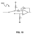
- FIG. 10 is a schematic diagram of one embodiment of a phase control element that may be used in a multichannel modulated optical system with cross-modulation compensation.
- a modulated optical system 100 with cross-modulation compensation is capable of reducing cross-modulation by varying bias current in response to cross-modulation detected on a multichannel RF signal.
- the modulated optical system 100 generally includes a laser 104 that receives a multichannel RF signal 106 from a multichannel RF source 102 .
- the laser 104 may include a RF input that receives the multichannel RF signal 106 , a bias current input that receives a bias current 108 , and an optical output that produces a modulated optical signal 109 in response to the RF signal 106 and the bias current 108 .
- the system 100 may also include other circuitry and/or components (not shown) between the multichannel RF source 102 and the laser 104 such as, for example, one or more predistortion circuits and a laser driver circuit.
- the modulated optical system 100 may be an optical transmitter such as a CATV transmitter.
- the system 100 may impart compensating cross-modulation with a magnitude substantially equal to the magnitude of the detected cross-modulation and with a phase that is substantially opposite the phase of the detected cross-modulation, thereby compensating for the detected cross-modulation.
- “compensate,” “compensation” or “compensating” for cross-modulation means reducing detected cross-modulation to a point that is tolerable in a particular system and does not necessarily require elimination of cross-modulation.
- the system 100 includes cross-modulation detection circuitry 110 that detects cross-modulation in the multichannel RF signal 106 from the multichannel RF source 102 and bias control circuitry 120 that controls the bias current 108 provided to the laser 104 .
- the cross-modulation detection circuitry 110 may be coupled to the RF signal path, for example, using a splitter 107 , such that the RF signal 106 is provided to the cross-modulation detection circuitry 110 and to the laser 104 .
- the cross-modulation detection circuitry 110 produces a cross-modulation detection signal 118 representing at least a portion of the cross-modulation on the multichannel RF signal 106 .
- the bias control circuitry 120 varies the bias current 108 in response to the cross-modulation detection signal 118 , which imparts compensating cross-modulation on the RF signal 106 provided to the laser 104 .
- the cross-modulation detection signal 118 may be used to modulate the bias current. Modulation of the bias current by the cross-modulation detection signal 118 causes fluctuations in the bias current, which cause the RF signal 106 to be modulated with compensating cross-modulation.
- the bias control circuitry 120 may vary the bias current, for example, such that the bias current changes in an opposite direction of the detected cross-modulation on the RF signal to impart the compensating cross-modulation that cancels out the detected cross-modulation.
- the multichannel RF signal 106 may include multiple superimposed modulated analog carriers at different frequencies.
- the multiple modulated analog carriers may be modulated using modulation techniques known to those skilled in the art, such as amplitude modulation, and may be combined using multiplexing techniques known to those skilled in the art, such as frequency division multiplexing.
- the multichannel RF signal 106 may also include one or more digital signals modulated using digital modulation, such as quadrature amplitude modulation (QAM).
- QAM quadrature amplitude modulation
- the resulting multichannel RF signal 106 occupies a bandwidth across the range of frequencies of the multiple modulated carriers.
- modulation and multiplexing techniques may be used to generate the multichannel RF signal 106 .
- the multichannel RF source 102 may include headend equipment in a CATV system and the multichannel RF signal 106 may be a downstream CATV signal.
- downstream multichannel CATV signals include 77 channels transmitted over a frequency range of about 50 MHz to 550 MHz and 110 channels transmitted over a frequency range of about 50 MHz to 750 MHz.
- Each channel in a downstream multichannel CATV signal may include a video carrier, a color subcarrier and an audio carrier. Other types of signals and frequency ranges may also be transmitted.
- Cross-modulation can occur when nonlinearities result in a carrier or channel in the multichannel RF signal 106 being modulated by the various signals carried on other channels in the same system.
- a group of video carriers may modulate other video carriers. Because each video channel contains a constant, high-level signal component at the horizontal line frequency (about 15.75 kHz in the NTSC system), this may be the most noticeable component of cross-modulation.
- the multichannel RF signal 106 which occupies a bandwidth across the range of frequencies of the multiple modulated carriers, directly modulates the laser 104 .
- Each channel in the multichannel RF signal 106 may be driven or modulated up to a certain optical modulation index (OMI) depending upon a desired channel-to-noise ratio (CNR).
- OMI optical modulation index
- CNR channel-to-noise ratio
- the OMI of at least some of the channels may be at least about 4% and more specifically about 5%.
- the system 200 generally includes a primary signal path 203 for carrying a multichannel RF signal 206 to a laser 204 and a secondary signal path 205 for providing the cross-modulation compensation.
- the secondary signal path 205 may be coupled to the primary signal path 203 , for example, using a splitter 207 .
- the system 200 includes envelope follower or detector circuitry 210 to detect cross-modulation on the RF signal 206 .
- the envelope follower or detector circuitry 210 receives the multichannel RF signal on the secondary signal path 205 and generates a cross-modulation detection signal that follows an envelope of the multichannel RF signal 206 .
- the changes in the envelope of the RF signal 206 may be indicative or representative of cross-modulation on the RF signal 206 .
- the envelope follower or detector circuitry 210 may include circuitry known to those skilled in the art for detecting an envelope of a high frequency RF signal.
- the envelope follower or detector circuitry 210 may include envelope detection circuitry that has a response time fast enough to detect an envelope of a multichannel RF signal.
- Envelope follower or detector circuitry 210 may be implemented using known envelope detection circuitry such as, for example, a precision rectifier circuit and a low pass filter. Specific implementations of envelope detection circuitry capable of detecting the envelope of such a signal are shown and described in U.S. patent application Ser. No. 12/053,104 and in U.S. patent application Ser. No. 11/753,082, which are fully incorporated herein by reference.
- the system 200 may also include one or more gain control elements 212 , such as a variable gain element and/or a variable attenuator, to provide gain and/or loss and thus controllably vary a magnitude of the cross-modulation detection signal generated by the envelope detection circuitry 210 .
- the gain control element(s) 212 may provide gain or loss depending upon how much compensating cross-modulation is needed to compensate for the detected cross-modulation. In other words, the gain control element(s) 212 may be used to provide gain or loss such that the magnitude of the compensating cross-modulation imparted to the RF signal corresponds sufficiently to the magnitude of the cross-modulation being compensated.
- the system 200 may further include one or more phase control elements 214 , such as a phase switch, to control a phase of the cross-modulation detection signal generated by the envelope detection circuitry 210 .
- the phase control element(s) 214 may change the phase as needed (e.g., by switching between positive and negative) to ensure that the phase of the compensating cross-modulation imparted to the RF signal is sufficiently out of phase with respect to the cross-modulation being compensated.
- a phase switch may be implemented using an inverted amplifier circuit 1000 , as shown in FIG. 10 , which is generally known to those skilled in the art.
- the phase control element 214 is shown following the gain control element 212 , the phase control element(s) 214 and gain control element(s) 212 may be arranged differently on the secondary signal path 205 .
- the system 200 further includes bias control circuitry 220 that adjusts or varies a bias current 208 in response to the cross-modulation detection signal that follows the envelope of the RF signal 206 and that has a magnitude and phase sufficient to compensate for the detected cross-modulation.
- the laser 204 receives both the RF signal on the primary signal path 203 and the varying bias current provided by the bias control circuitry 220 and generates a modulated optical signal in response thereto.
- the bias control circuitry 220 may also adjust the bias current in response to other signals, such as an anti-clipping signal and/or a power monitor signal.
- the bias control circuitry 220 may include circuitry know to those of ordinary skill in the art for providing a bias current to a directly modulated laser.
- the system 200 may also include a delay element (not shown) in the primary signal path 203 such that the RF signal is delayed to reduce or eliminate this lag.
- the delay element may not be needed, however, when the cross modulation is predominantly the 15.75 kHz signal component because the RF delay is relatively short.
- the modulated optical system 200 ′ includes an RF power detector 211 to detect the cross-modulation on the RF signal.
- the RF power detector 211 receives the multichannel RF signal on the secondary signal path 205 , detects fluctuations in the RF power, and generates a cross-modulation detection signal that varies with the detected power fluctuations. Similar to the envelope of the RF signal, fluctuations in the RF power may be indicative or representative of cross-modulation on the RF signal.
- the RF power detector 211 may include circuitry known to those skilled in the art for detecting power fluctuations in a RF signal, such as a 50 MHz to 3 GHz monolithic RF power detector capable of measuring RF signals over a 60 dB dynamic range.
- One such RF power detector is available from Linear Technology Corporation under the name LT®5534.
- the magnitude and/or phase may then be adjusted using gain control element(s) 212 and/or phase control element(s) 214 as described above.
- the bias control circuitry 220 may then vary the bias current provided to the laser 204 in response to the cross modulation detection signal that varies in response to RF power fluctuations.
- FIGS. 3A-3D illustrate one example of the generation of a cross-modulation detection signal 318 from a multichannel RF signal 306 .
- FIG. 3A illustrates a multichannel RF signal 306 with cross-modulation.
- the illustrated RF signal 306 includes periods 301 of lower power and periods 303 of higher power.
- FIG. 3B illustrates the cross-modulation detection signal 318 generated by cross-modulation detection circuitry, such as an envelope detector or RF power detector.
- the cross-modulation detection signal 318 generally corresponds to the envelope or power fluctuations of the RF signal 306 and is indicative of the cross-modulation on the RF signal 306 .
- FIG. 3C illustrates the cross-modulation detection signal 318 with changes in magnitude that may be provided, for example, by the gain control element(s) 212 shown in FIGS. 2A and 2B .
- Providing gain results in a cross-modulation detection signal 318 a with increased magnitude.
- Providing loss or attenuation results in a cross-modulation signal 318 b with a decreased magnitude.
- the magnitude of the cross-modulation detection signal 318 may be adjusted depending upon the cross-modulation to be compensated.
- FIG. 3D illustrates the cross-modulation detection signal 318 with changes in phase that may be provided, for example, by the phase control element(s) 214 shown in FIGS. 2A and 2B . Adjusting the phase results in a cross-modulation detection signal 318 c with a different phase than the cross-modulation detection signal 318 .
- the phase of the cross-modulation detection signal 318 may be adjusted depending upon the cross-modulation to be compensated.
- the phase may be changed such that the phase-adjusted cross-modulation detection signal 318 c is inverted relative to the cross-modulation detection signal 318 .
- the phase may be kept the same as the cross-modulation detection signal 318 .
- a further embodiment of a modulated optical system 400 with cross-modulation compensation may also provide anti-clipping.
- the sum of the voltage of the aligned carriers may result in a peak voltage condition.
- OMI optical modulation index
- the peak voltage condition may result in a higher occurrence of negative voltage spikes or peaks that cause the laser input current to fall below a threshold current of a laser 404 , resulting in clipping.
- the system 400 may include cross-modulation detection circuitry 410 that provides cross-modulation detection signal 418 , for example, as described above, and anti-clipping circuitry 430 that provides an anti-clipping signal 432 .
- the cross-modulation detection circuitry 410 and the anti-clipping circuitry 430 receive the RF signal 406 from a multichannel RF source 402 and generate the respective cross-modulation detection signal 418 and anti-clipping signal 432 in response thereto.
- Bias control circuitry 420 may adjust a bias current 408 provided to laser 404 in response to the cross-modulation detection signal 418 and/or the anti-clipping signal 432 .
- the varying bias current 408 may thus cause compensation of cross-modulation, as described above, and/or a reduction of clipping.
- to reduce or correct clipping means to prevent one or more negative spikes or peaks in the multichannel RF signal from causing clipping in the laser 404 and does not require a complete elimination of clipping.
- the anti-clipping circuitry 430 includes envelope follower circuitry that receives the multichannel RF signal 406 , detects an envelope of the RF signal 406 , and generates the anti-clipping signal 432 in response to the detected envelope.
- the bias current 408 may be adjusted or varied inversely proportional to a detected lower envelope of the multichannel RF signal. In particular, the bias current 408 may be increased as a lower envelope of the multichannel RF signal 406 falls and indicates a peak negative voltage condition.
- the bias current 408 should be increased to a level that will prevent that negative peak and/or subsequent negative peak(s) from causing clipping.
- Embodiments of anti-clipping circuitry are described in greater detail in U.S. patent application Ser. No. 12/053,104 and in U.S. patent application Ser. No. 11/753,082, which are fully incorporated herein by reference.
- a modulated optical system 500 with cross-modulation compensation is capable of compensating cross-modulation at a target frequency range.
- target frequency range may include a single frequency or a range of multiple frequencies.
- a significant component of cross-modulation in a CATV RF signal is at the horizontal line frequency (about 15.75 kHz in the NTSC system).
- the modulated optical system 500 may thus provide cross-modulation compensation at the horizontal line frequency.
- Cross-modulation compensation may also be provided at other horizontal line frequencies or other target frequencies.
- the modulated optical system 500 generally includes a laser 504 that receives a multichannel RF signal 506 from a multichannel RF source 502 .
- the laser 504 may include a RF input that receives the multichannel RF signal 506 , a bias current input that receives a bias current 508 , and an optical output that produces a modulated optical signal 509 in response to the RF signal 506 and the bias current 508 .
- the system 500 may also include other circuitry and/or components (not shown) between the multichannel RF source 502 and the laser 504 such as, for example, one or more predistortion circuits and a laser driver circuit.
- the modulated optical system 500 may be an optical transmitter such as a CATV transmitter.
- the system 500 also includes filtered cross-modulation detection circuitry 510 that detects cross-modulation in the multichannel RF signal 506 from the multichannel RF source 502 and cross-modulation compensation circuitry 520 that imparts compensating cross-modulation to the RF signal 506 .
- the cross-modulation detection circuitry 510 may be coupled to the RF signal path, for example, using a splitter 507 , such that the RF signal 506 is provided to the cross-modulation detection circuitry 510 and to the laser 504 .
- the cross-modulation detection circuitry 510 produces a filtered cross-modulation detection signal 518 representing at least a portion of the cross-modulation on the multichannel RF signal 506 at the target frequency range.
- the cross-modulation compensation circuitry 520 modulates the RF signal 506 provided to the laser 504 in response to the filtered cross-modulation compensation signal 518 .
- the modulation of the RF signal 506 imparts the compensating cross-modulation to compensate for the detected cross-modulation component at the target frequency range.
- FIGS. 6-8 illustrate different embodiments of modulated optical systems 600 , 700 , 800 that provide cross-modulation compensation at a target frequency range.
- the modulated optical system 600 shown in FIG. 6 compensates for cross-modulation at the target frequency range by adjusting the bias current provided to a laser 604 .
- the system 600 generally includes a primary signal path 603 for carrying a multichannel RF signal 606 to the laser 604 and a secondary signal path 605 for providing the cross-modulation compensation by varying the bias current.
- the secondary signal path 605 may be coupled to the primary signal path 603 , for example, using a splitter 607 .
- the system 600 includes cross-modulation detection circuitry 610 , such as envelope detection circuitry or RF power detection circuitry, to detect the cross-modulation on the RF signal, as described above.
- the cross-modulation detection circuitry 610 receives the multichannel RF signal 606 on the secondary signal path 605 and generates a cross-modulation detection signal that follows an envelope of the RF signal 606 and/or varies with the detected power fluctuations of the RF signal 606 .
- the system 600 includes a filter 611 to filter the cross-modulation detection signal generated by the cross-modulation detection circuitry 610 at the target frequency range.
- the filter 611 may be a bandpass filter that passes frequencies within the target frequency range. If the target frequency range is the 15.75 kHz horizontal line frequency, for example, a 15.75 kHz bandpass filter may be used.
- the cross-modulation detection signal generated by the cross-modulation detection circuitry 610 (e.g., by following the envelope of the RF signal or by detecting power fluctuations in the RF signal) may include components at lower and higher frequencies that do not require compensation.
- the filter 611 may improve the cross-modulation compensation by removing these higher and lower frequencies and passing a frequency or frequencies within the target frequency range. Thus, compensation of cross-modulation is improved by focusing on the target frequency range where cross-modulation may have a greater impact.
- the system 600 may also include one or more gain control elements 612 and one or more phase control elements 614 , as described above, to control a magnitude and/or phase of the cross-modulation detection signal as needed to ensure that the magnitude and phase are sufficient to impart compensating cross-modulation.
- the gain control elements 612 and phase control elements 614 may follow the filter 611 such that the gain and phase of the cross-modulation detection signal is controlled at the target frequency range, which improves cross-modulation performance.
- the system 600 further includes bias control circuitry 620 that adjusts or varies a bias current to the laser 604 in response to the filtered cross-modulation detection signal that has a magnitude and phase sufficient to compensate for the detected cross-modulation at the target frequency range.
- the laser 604 receives both the RF signal on the primary signal path 603 and the varying bias current provided by the bias control circuitry 620 and generates a modulated optical signal in response thereto.
- the varying bias current is combined with the RF signal, compensating cross-modulation is imparted on the RF signal and compensates for the detected cross-modulation, as described above.
- the modulated optical system 700 shown in FIG. 7 compensates for cross-modulation at the target frequency range by directly modulating the RF signal 706 on a primary signal path 703 before the RF signal 706 modulates a laser 704 .
- the system 700 includes a secondary signal path 705 with cross-modulation detection circuitry 710 , filter 711 , gain control element(s) 712 , and phase control element(s) 714 , which produce the filtered cross-modulation detection signal having the desired magnitude and phase.
- the system 700 includes a variable gain control element 740 coupled to the primary signal path 703 for varying attenuation and/or gain of the RF signal 706 in response to the filtered cross-modulation detection signal. By varying the attenuation and/or gain of the RF signal 706 in response to the filtered cross-modulation detection signal, compensating cross-modulation is imparted to the RF signal 706 on the primary signal path 703 .
- the system 700 may also include bias control circuitry 720 that separately controls the bias current to the laser 704 (e.g., in response to a monitored power output of the laser 704 or in response to an anti-clipping signal).
- the modulated optical system 800 shown in FIG. 8 provides anti-clipping and compensates for cross-modulation at the target frequency range by directly modulating a RF signal 806 .
- the system 800 may include anti-clipping circuitry 810 that adjusts the bias current provided by a DC source 820 to a laser 804 .
- the anti-clipping circuitry 810 may include a peak detector 812 , an amplifier 814 , and a signal limiter 816 .
- the peak detector 812 produces an output signal that is proportional to the frequency of occurrence and intensity of peaks in the RF signal 806 that are likely to cause clipping in the laser 804 .
- the amplifier 814 adjusts the amplitude of the output signal from the peak detector 812 to a level suitable for varying the bias current to the laser 804 .
- the signal limiter 816 may limit the maximum positive and negative signal amplitudes to preset levels to counter any negative effects of excessive laser bias.
- One example of the anti-clipping circuitry 810 is described in greater detail in U.S. Pat. No. 6,549,316, which is fully incorporated herein by reference.
- the changes in bias current caused by the anti-clipping circuit 810 may result in cross-modulation on the RF signal 806 modulating the laser 804 .
- the cross-modulation may have a significant component at a certain frequency or frequencies (e.g., at the 15.75 kHz frequency corresponding to the horizontal line frequency in a NTSC system).
- the anti-clipping signal from the anti-clipping circuitry 810 may be fed back to a voltage variable attenuator 840 , which modulates the input RF signal 806 to impart a compensating cross-modulation (i.e., substantially equal in magnitude but opposite in phase).
- the system 800 may include an amplifier 830 that amplifies the anti-clipping signal to a level suitable for input to the voltage variable attenuator 840 and a filter 811 , such as a bandpass filter, that filters the anti-clipping signal at the target frequency range (e.g., at 15.75 kHz).
- a filter 811 such as a bandpass filter, that filters the anti-clipping signal at the target frequency range (e.g., at 15.75 kHz).
- the voltage variable attenuator 840 may provide the compensating cross-modulation only at the target frequency range.
- FIGS. 9A-9E illustrate one example of the generation of a cross-modulation detection signal 918 from a multichannel RF signal 906 .
- FIG. 9A illustrates a multichannel RF signal 906 with cross-modulation. The illustrated RF signal 906 includes periods 901 of lower power and periods 903 of higher power.
- FIG. 9B illustrates the cross-modulation detection signal 918 generated by cross-modulation detection circuitry, such as an envelope detector or RF power detector.
- the cross-modulation detection signal 918 generally corresponds to the envelope or power fluctuations of the RF signal 906 and is indicative of the cross-modulation on the RF signal 906 .
- FIG. 9C illustrates the filtered cross-modulation detection signal 918 a , for example, after the cross-modulation detection signal 918 is filtered by a bandpass filter at the target frequency range.
- FIG. 9D illustrates the filtered cross-modulation detection signal 918 b with an increase in magnitude, for example, after the filtered cross-modulation detection signal 918 a is provided with gain.
- FIG. 9D illustrates the filtered cross-modulation detection signal 918 c with a phase change of ⁇ relative to the filtered cross-modulation detection signal 918 b .
- the filtered cross-modulation detection signal 918 c with the adjusted magnitude and phase may then be used to compensate for cross-modulation at the target frequency range, for example, by varying a bias current or directly modulating the RF signal 906 , as described above.
- systems and methods may compensate for cross-modulation in a multichannel RF signal at a target frequency range.
- a modulated optical system with cross-modulation compensation.
- the system includes a laser including a RF input configured to receive a multichannel RF signal, a bias input configured to receive a bias current, and an optical output configured to provide a modulated optical signal in response to the multichannel RF signal and the bias current.
- the multichannel RF signal includes a superposition of multiple carriers, and at least one of the multiple carriers modulates at least one other of the multiple carriers resulting in cross-modulation.
- the modulated optical system also includes cross-modulation detection circuitry configured to receive the multichannel RF signal and to generate a cross-modulation detection signal responsive to the multichannel RF signal.
- the cross-modulation detection circuitry includes a filter configured to filter the cross-modulation detection signal and to generate a filtered cross-modulation detection signal at a target frequency range at which a cross-modulation component occurs.
- the modulated optical system further includes cross-modulation compensation circuitry configured to modulate the multichannel RF signal provided to the laser in response to the filtered cross-modulation compensation signal such that compensating cross-modulation is imparted to the multichannel RF signal to compensate for the cross-modulation component at the target frequency range.
- a method for reducing cross-modulation in a modulated optical system.
- the method includes: providing a multichannel RF signal to a laser diode, the multichannel RF signal including a superposition of multiple carriers, and wherein at least one of the multiple carriers modulates at least one other of the multiple carriers resulting in cross-modulation; receiving a portion of the RF signal on at least one secondary signal path; generating a cross-modulation detection signal responsive to the multichannel RF signal on the secondary signal path; filtering the cross-modulation detection signal to generate a filtered cross-modulation detection signal at a target frequency range at which a cross-modulation component occurs; modulating the multichannel RF signal provided to the laser in response to the filtered cross-modulation detection signal such that compensating cross-modulation is imparted to the multichannel RF signal to compensate for the cross-modulation component at the target frequency range; and providing a modulated optical signal from the laser.
Abstract
Description
Claims (23)
Priority Applications (1)
| Application Number | Priority Date | Filing Date | Title |
|---|---|---|---|
| US12/245,028 US8320773B2 (en) | 2008-10-03 | 2008-10-03 | Reducing cross-modulation in multichannel modulated optical systems |
Applications Claiming Priority (1)
| Application Number | Priority Date | Filing Date | Title |
|---|---|---|---|
| US12/245,028 US8320773B2 (en) | 2008-10-03 | 2008-10-03 | Reducing cross-modulation in multichannel modulated optical systems |
Publications (2)
| Publication Number | Publication Date |
|---|---|
| US20100086309A1 US20100086309A1 (en) | 2010-04-08 |
| US8320773B2 true US8320773B2 (en) | 2012-11-27 |
Family
ID=42075913
Family Applications (1)
| Application Number | Title | Priority Date | Filing Date |
|---|---|---|---|
| US12/245,028 Active 2031-05-20 US8320773B2 (en) | 2008-10-03 | 2008-10-03 | Reducing cross-modulation in multichannel modulated optical systems |
Country Status (1)
| Country | Link |
|---|---|
| US (1) | US8320773B2 (en) |
Cited By (1)
| Publication number | Priority date | Publication date | Assignee | Title |
|---|---|---|---|---|
| US20160028482A1 (en) * | 2014-07-25 | 2016-01-28 | Arris Enterprises, Inc. | Hybrid laser anti-clipping for fiber-coaxial networks |
Families Citing this family (3)
| Publication number | Priority date | Publication date | Assignee | Title |
|---|---|---|---|---|
| US8606116B2 (en) * | 2011-01-13 | 2013-12-10 | Applied Optoelectronics, Inc. | System and method for distortion compensation in response to frequency detection |
| JP6332977B2 (en) * | 2014-01-20 | 2018-05-30 | 国立大学法人富山大学 | QAM modulation method, QAM modulation apparatus, and CATV system using the same |
| US9590732B2 (en) * | 2014-04-21 | 2017-03-07 | Arris Enterprises, Inc. | Active optical combiner for CATV network |
Citations (7)
| Publication number | Priority date | Publication date | Assignee | Title |
|---|---|---|---|---|
| US5703530A (en) | 1995-10-06 | 1997-12-30 | Yagi Antenna Co., Ltd. | Radio frequency amplifier having improved CTB and cross modulation characteristics |
| WO2000014887A1 (en) | 1998-09-09 | 2000-03-16 | Ortel Corporation | Electronic circuit for correcting cross modulation distortion |
| US6118479A (en) | 1998-01-23 | 2000-09-12 | Matsushita Electric Industrial Co., Ltd. | Optical transmission method, error rate evaluation method applied in optical transmission and apparatus for generating a signal for error rate evaluation |
| US6549316B2 (en) | 1998-12-15 | 2003-04-15 | Agere Systems, Inc. | Circuit for suppressing noise and distortion in linear fiber optic links |
| US6577177B2 (en) | 1999-04-01 | 2003-06-10 | General Instrument Corporation | Non-linear distortion generator |
| US6728277B1 (en) * | 2000-08-28 | 2004-04-27 | Emcore Corporation | Envelope biasing for laser transmitters |
| US7873285B2 (en) * | 2007-05-23 | 2011-01-18 | General Instrument Corporation | Anti clipping circuit for laser transmitters |
-
2008
- 2008-10-03 US US12/245,028 patent/US8320773B2/en active Active
Patent Citations (7)
| Publication number | Priority date | Publication date | Assignee | Title |
|---|---|---|---|---|
| US5703530A (en) | 1995-10-06 | 1997-12-30 | Yagi Antenna Co., Ltd. | Radio frequency amplifier having improved CTB and cross modulation characteristics |
| US6118479A (en) | 1998-01-23 | 2000-09-12 | Matsushita Electric Industrial Co., Ltd. | Optical transmission method, error rate evaluation method applied in optical transmission and apparatus for generating a signal for error rate evaluation |
| WO2000014887A1 (en) | 1998-09-09 | 2000-03-16 | Ortel Corporation | Electronic circuit for correcting cross modulation distortion |
| US6549316B2 (en) | 1998-12-15 | 2003-04-15 | Agere Systems, Inc. | Circuit for suppressing noise and distortion in linear fiber optic links |
| US6577177B2 (en) | 1999-04-01 | 2003-06-10 | General Instrument Corporation | Non-linear distortion generator |
| US6728277B1 (en) * | 2000-08-28 | 2004-04-27 | Emcore Corporation | Envelope biasing for laser transmitters |
| US7873285B2 (en) * | 2007-05-23 | 2011-01-18 | General Instrument Corporation | Anti clipping circuit for laser transmitters |
Cited By (2)
| Publication number | Priority date | Publication date | Assignee | Title |
|---|---|---|---|---|
| US20160028482A1 (en) * | 2014-07-25 | 2016-01-28 | Arris Enterprises, Inc. | Hybrid laser anti-clipping for fiber-coaxial networks |
| US9485021B2 (en) * | 2014-07-25 | 2016-11-01 | Arris Enterprises, Inc. | Hybrid laser anti-clipping for fiber-coaxial networks |
Also Published As
| Publication number | Publication date |
|---|---|
| US20100086309A1 (en) | 2010-04-08 |
Similar Documents
| Publication | Publication Date | Title |
|---|---|---|
| US6549316B2 (en) | Circuit for suppressing noise and distortion in linear fiber optic links | |
| US8165474B2 (en) | Reducing cross modulation in multichannel modulated optical systems with anti-clipping | |
| TWI416184B (en) | Directly modulated laser optical transmission system with phase modulation | |
| US5680238A (en) | Hybrid SCM optical transmission apparatus | |
| US5808512A (en) | Feed forward amplifiers and methods | |
| US7881621B2 (en) | Optical transmission system with directly modulated laser and feed forward noise cancellation | |
| US6687466B1 (en) | Dynamic distortion control | |
| US5861777A (en) | Method and apparatus for compensation of phase distortion in power amplifiers | |
| US8023830B2 (en) | Externally modulated laser optical transmission system with feed forward noise cancellation | |
| US8606116B2 (en) | System and method for distortion compensation in response to frequency detection | |
| US8320773B2 (en) | Reducing cross-modulation in multichannel modulated optical systems | |
| US20070134001A1 (en) | Polarization division multiplexed optical transmission system | |
| USRE44647E1 (en) | Directly modulated laser optical transmission system with phase modulation | |
| JPH09246641A (en) | Clipping distortion control circuit | |
| US6181453B1 (en) | Method and apparatus for laser performance enhancement | |
| US9191111B2 (en) | Reducing cross-modulation in multichannel modulated optical systems | |
| JP5512090B2 (en) | Direct modulation or external modulation laser light transmission system with feedforward noise cancellation | |
| US20080292323A1 (en) | Systems and methods for reducing clipping in multichannel modulated optical systems | |
| JP5847771B2 (en) | Direct modulation or external modulation laser light transmission system with feedforward noise cancellation | |
| US5448392A (en) | Process for the optical transmission of a multiplex of electrical carriers and apparatus for performing such a process | |
| US8358937B2 (en) | Systems and methods for reducing clipping in multichannel modulated optical systems | |
| JPH10511186A (en) | Light emitting head including laser and modulator | |
| US20070134000A1 (en) | Polarization division multiplexed optical transmission system | |
| Pophillat | Optical modulation depth improvement in SCM lightwave systems using a dissymmetrization scheme | |
| JP3557153B2 (en) | Optical transmitter |
Legal Events
| Date | Code | Title | Description |
|---|---|---|---|
| AS | Assignment |
Owner name: APPLIED OPTOELECTRONICS, INC.,TEXAS Free format text: ASSIGNMENT OF ASSIGNORS INTEREST;ASSIGNORS:ZHENG, JUN;TSAI, CHAO-HUNG;REEL/FRAME:022148/0008 Effective date: 20081218 Owner name: APPLIED OPTOELECTRONICS, INC., TEXAS Free format text: ASSIGNMENT OF ASSIGNORS INTEREST;ASSIGNORS:ZHENG, JUN;TSAI, CHAO-HUNG;REEL/FRAME:022148/0008 Effective date: 20081218 |
|
| AS | Assignment |
Owner name: EAST WEST BANK, SUCCESSOR IN INTEREST TO UNITED CO Free format text: SECURITY AGREEMENT;ASSIGNOR:APPLIED OPTOELECTRONICS, INC.;REEL/FRAME:024332/0828 Effective date: 20070906 |
|
| STCF | Information on status: patent grant |
Free format text: PATENTED CASE |
|
| AS | Assignment |
Owner name: EAST WEST BANK, CALIFORNIA Free format text: SECURITY INTEREST;ASSIGNOR:APPLIED OPTOELECTRONICS, INC.;REEL/FRAME:036047/0293 Effective date: 20150630 |
|
| FPAY | Fee payment |
Year of fee payment: 4 |
|
| AS | Assignment |
Owner name: BRANCH BANKING AND TRUST COMPANY, TEXAS Free format text: SECURITY INTEREST;ASSIGNOR:APPLIED OPTOELECTRONICS, INC.;REEL/FRAME:044061/0812 Effective date: 20170928 |
|
| AS | Assignment |
Owner name: APPLIED OPTOELECTRONICS INC, TEXAS Free format text: RELEASE BY SECURED PARTY;ASSIGNOR:EAST WEST BANK, SUCCESSOR IN INTEREST TO UNITED COMMERCIAL BANK;REEL/FRAME:043800/0480 Effective date: 20171005 Owner name: APPLIED OPTOELECTRONICS INC, TEXAS Free format text: RELEASE BY SECURED PARTY;ASSIGNOR:EAST WEST BANK;REEL/FRAME:044207/0573 Effective date: 20171005 |
|
| MAFP | Maintenance fee payment |
Free format text: PAYMENT OF MAINTENANCE FEE, 8TH YEAR, LARGE ENTITY (ORIGINAL EVENT CODE: M1552); ENTITY STATUS OF PATENT OWNER: LARGE ENTITY Year of fee payment: 8 |
|
| AS | Assignment |
Owner name: APPLIED OPTOELECTRONICS, INC., TEXAS Free format text: RELEASE BY SECURED PARTY;ASSIGNOR:TRUIST BANK (FORMERLY KNOWN AS BRANCH BANKING AND TRUST COMPANY));REEL/FRAME:061952/0344 Effective date: 20221116 |
|
| AS | Assignment |
Owner name: CIT NORTHBRIDGE CREDIT LLC, NEW YORK Free format text: PATENT SECURITY AGREEMENT;ASSIGNOR:APPLIED OPTOELECTRONICS, INC.;REEL/FRAME:062003/0523 Effective date: 20221116 |
|
| AS | Assignment |
Owner name: APPLIED OPTOELECTRONICS, INC., TEXAS Free format text: TERMINATION AND RELEASE OF SECURITY INTEREST IN PATENTS;ASSIGNOR:CIT NORTHBRIDGE CREDIT LLC;REEL/FRAME:065630/0906 Effective date: 20231117 |