US8327082B2 - Snoop request arbitration in a data processing system - Google Patents
Snoop request arbitration in a data processing system Download PDFInfo
- Publication number
- US8327082B2 US8327082B2 US12/201,225 US20122508A US8327082B2 US 8327082 B2 US8327082 B2 US 8327082B2 US 20122508 A US20122508 A US 20122508A US 8327082 B2 US8327082 B2 US 8327082B2
- Authority
- US
- United States
- Prior art keywords
- snoop
- cache
- queue
- fullness
- request
- Prior art date
- Legal status (The legal status is an assumption and is not a legal conclusion. Google has not performed a legal analysis and makes no representation as to the accuracy of the status listed.)
- Expired - Fee Related, expires
Links
- 238000012545 processing Methods 0.000 title claims description 151
- 230000015654 memory Effects 0.000 claims description 40
- 238000000034 method Methods 0.000 claims description 24
- 230000004044 response Effects 0.000 claims description 19
- 239000004020 conductor Substances 0.000 description 16
- 238000010586 diagram Methods 0.000 description 15
- 235000003642 hunger Nutrition 0.000 description 11
- 230000037351 starvation Effects 0.000 description 11
- 230000007704 transition Effects 0.000 description 11
- 230000002457 bidirectional effect Effects 0.000 description 5
- 230000006870 function Effects 0.000 description 4
- 239000000872 buffer Substances 0.000 description 3
- 239000004065 semiconductor Substances 0.000 description 3
- 230000009471 action Effects 0.000 description 2
- 230000008901 benefit Effects 0.000 description 2
- 230000005540 biological transmission Effects 0.000 description 2
- 230000001427 coherent effect Effects 0.000 description 2
- 230000008878 coupling Effects 0.000 description 2
- 238000010168 coupling process Methods 0.000 description 2
- 238000005859 coupling reaction Methods 0.000 description 2
- 238000007726 management method Methods 0.000 description 2
- 239000000463 material Substances 0.000 description 2
- 230000007246 mechanism Effects 0.000 description 2
- 238000012986 modification Methods 0.000 description 2
- 230000004048 modification Effects 0.000 description 2
- 229910052710 silicon Inorganic materials 0.000 description 2
- 239000010703 silicon Substances 0.000 description 2
- 230000001360 synchronised effect Effects 0.000 description 2
- 238000012546 transfer Methods 0.000 description 2
- 241001522296 Erithacus rubecula Species 0.000 description 1
- 238000000354 decomposition reaction Methods 0.000 description 1
- 230000001419 dependent effect Effects 0.000 description 1
- 238000001514 detection method Methods 0.000 description 1
- 230000000694 effects Effects 0.000 description 1
- 230000005294 ferromagnetic effect Effects 0.000 description 1
- 230000010365 information processing Effects 0.000 description 1
- 230000005291 magnetic effect Effects 0.000 description 1
- 230000005055 memory storage Effects 0.000 description 1
- 238000012544 monitoring process Methods 0.000 description 1
- 230000003287 optical effect Effects 0.000 description 1
- 238000012913 prioritisation Methods 0.000 description 1
- 230000008569 process Effects 0.000 description 1
- 230000002123 temporal effect Effects 0.000 description 1
Images


Classifications
-
- G—PHYSICS
- G06—COMPUTING; CALCULATING OR COUNTING
- G06F—ELECTRIC DIGITAL DATA PROCESSING
- G06F12/00—Accessing, addressing or allocating within memory systems or architectures
- G06F12/02—Addressing or allocation; Relocation
- G06F12/08—Addressing or allocation; Relocation in hierarchically structured memory systems, e.g. virtual memory systems
- G06F12/0802—Addressing of a memory level in which the access to the desired data or data block requires associative addressing means, e.g. caches
- G06F12/0806—Multiuser, multiprocessor or multiprocessing cache systems
- G06F12/0815—Cache consistency protocols
- G06F12/0831—Cache consistency protocols using a bus scheme, e.g. with bus monitoring or watching means
-
- G—PHYSICS
- G06—COMPUTING; CALCULATING OR COUNTING
- G06F—ELECTRIC DIGITAL DATA PROCESSING
- G06F2212/00—Indexing scheme relating to accessing, addressing or allocation within memory systems or architectures
- G06F2212/10—Providing a specific technical effect
- G06F2212/1016—Performance improvement
Definitions
- This disclosure relates generally to data processing systems, and more specifically, to cache coherency in a data processing system.
- Some data processing systems use multiple processors with closely coupled cache memories.
- a cache memory stores a subset of duplicative information that is stored in the system memory.
- Using a cache in the system may reduce the number of occurrences that a processor must communicate with the system memory via a system interconnect.
- the presence of various caches (or other memory devices) in a system can readily permit a data operand which has the same identifier or address to be present at various locations in the system.
- Memory coherency refers to the need of each processor in a multiple master data processing system to have access to the most recently modified data corresponding to a particular address in the memory system.
- the presence of differing data values for a same address value in a data processing system may lead to system errors.
- reads and writes of information to the system memory are monitored or “snooped”.
- this address of the transaction is used as a snoop address.
- a snoop request is initiated and directed to all caches in the system such that snoop lookups can be performed to search for any address in the caches that match the snoop address.
- a snoop hit occurs for every match, and any needed corrective action is taken to maintain coherency of the data at the address in the cache where the snoop hit occurs.
- arbitration is needed between processor requests to search for addresses in its own cache (such as for performing a load or store instruction whose corresponding access address may be contained in the cache) and snoop requests to perform snoop lookups in the cache.
- any pending snoop request blocks the processor from accessing its cache for one or more cycles. If snoop lookups occur frequently, then processor performance may be negatively impacted.
- FIG. 1 is a block diagram of a data processing system according to one embodiment of the present invention.
- FIG. 2 is a block diagram of one embodiment of a portion of a processor according to one embodiment of the present invention.
- FIG. 3 is a block diagram of a portion of a cache according to one embodiment of the present invention.
- FIG. 4 is a timing diagram according to one embodiment of the present invention.
- FIG. 5 illustrates a block diagram of a portion of an arbiter which may be used for the arbiter of FIG. 3 in accordance with one embodiment of the present invention
- FIG. 6 illustrates a timing diagram according to one embodiment of the present invention.
- FIG. 7 illustrates a block diagram of a portion of an arbiter which may be used for the arbiter of FIG. 3 in accordance with one embodiment of the present invention.
- FIG. 8 illustrates a timing diagram according to one embodiment of the present invention.
- snoop requests which are buffered in a snoop queue, are only performed when there is an idle processor cycle available or when a certain snoop queue fullness has been reached. This may allow a processor to have almost uninterrupted access to its cache, and may reduce the penalty of snoop look-ups.
- the arbiter which arbitrates requests to the cache from the processor and from the snoop queue, can monitor both processor requests to the cache and a fullness level of the snoop queue to decide when to handle queued snoop requests. Therefore, in one embodiment, until a predetermined number of snoop requests are buffered in the snoop queue, the processor is not stalled to process snoop requests.
- the arbiter may elevate the priority of snoop queue entries above the processor requests until the snoop queue fullness has been reduced to the predetermined number or less.
- this type of snoop protocol may be referred to as a lazy snoop protocol in which an immediate snoop lookup is not required when a snoop request is received.
- one or more counters are used to ensure that starvation of the processor or the snoop queue is avoided.
- bus is used to refer to a plurality of signals or conductors which may be used to transfer one or more various types of information, such as data, addresses, control, or status.
- the conductors as discussed herein may be illustrated or described in reference to being a single conductor, a plurality of conductors, unidirectional conductors, or bidirectional conductors. However, different embodiments may vary the implementation of the conductors. For example, separate unidirectional conductors may be used rather than bidirectional conductors and vice versa.
- plurality of conductors may be replaced with a single conductor that transfers multiple signals serially or in a time multiplexed manner. Likewise, single conductors carrying multiple signals may be separated out into various different conductors carrying subsets of these signals. Therefore, many options exist for transferring signals.
- FIG. 1 illustrates, in block diagram form, a data processing system 10 according to one embodiment of the present invention.
- Data processing system 10 includes processor 14 , processor 16 , cache coherency manager 18 , system transaction arbiter 32 , system memory 20 , other master devices 22 , other slave devices 24 , input/output (I/O) devices 26 , and a system monitor 13 .
- the devices shown in FIG. 1 are communicatively coupled to a system interconnect bus 12 but maybe coupled by other types of system interconnects in other embodiments.
- the devices shown may be communicatively coupled by a system interconnect that includes a cross bar switch or other type of switch, or a system interconnect that includes multiple busses and/or switches.
- a system interconnect bus may include multiple signal lines for address, data, and control information.
- System transaction arbiter 32 arbitrates among various masters of system 10 for transactions on a system interconnect bus 12 .
- I/O devices 26 may be any number of I/O devices such as keyboard controllers and communications ports.
- Other slave devices 24 may include memory devices such as a system cache (e.g. L2 cache). Both devices 24 and 26 may be accessible by transactions on system interconnect bus 12 that are generated by the master devices of the system (e.g. processor 14 , processor 16 , or other master devices 22 ).
- other master devices 22 includes other types of processors (e.g. a digital signal processor) or a direct memory access (DMA) device which can generate transactions on system interconnect bus 12 .
- each master device may also include a cache (not shown).
- System 10 includes a cache coherency manager 18 that snoops system interconnect bus 12 for transactions and initiates snoop requests for various caches of system 10 (e.g. cache 28 , cache 30 ) to determine whether the caches include the data operand (e.g. access address) of the transaction in order to maintain cache coherency. In one embodiment, if a cache contains a copy of the data operand, then that cache will invalidate the corresponding cache entry in response to the snoop request.
- cache coherency manager 18 that snoops system interconnect bus 12 for transactions and initiates snoop requests for various caches of system 10 (e.g. cache 28 , cache 30 ) to determine whether the caches include the data operand (e.g. access address) of the transaction in order to maintain cache coherency. In one embodiment, if a cache contains a copy of the data operand, then that cache will invalidate the corresponding cache entry in response to the snoop request.
- a transaction is a write transaction by processor 16 to system memory 20 for writing data to a location in memory 20 .
- cache coherency manager 18 would generate a snoop request to the other caches (e.g. cache 28 ) to search for data of the same memory address. If a cache has an entry corresponding to the same memory address, then the cache would invalidate that data since an updated version is being provided to memory 20 on system interconnect bus 12 .
- system 10 includes a snoop control interface between the cache coherency manager 18 and each of the processors 14 and 16 for exchanging information regarding snooping operations.
- the snoop control interface includes snoop request lines and snoop status. Alternate embodiments may include more or different lines within the snoop control interface. These lines will be discussed below.
- cache coherency manager 18 only includes snoop control interfaces with processors 14 and 16 . However, in other embodiments, cache coherency manager 18 may include a snoop control interface with other devices having a cache (e.g. master devices 22 , slave devices 24 , and other caches). In alternative embodiments, processors 14 and 16 may include additional caches.
- system 10 also includes a system monitor 13 .
- System monitor 13 may be, for example, a performance monitor or a global throughput monitor. Any known performance monitor or global throughput monitor may be used, where information from system monitor 13 can be used, for example, by one or more masters on the bus to alter one or more parameters. Additional details of system monitor 13 will be discussed below.
- other types of data systems may include different configurations and/or have additional circuitry.
- other embodiments may not have all of the circuitry shown in FIG. 1 .
- some or all of the circuitry shown in FIG. 1 may be implemented on one integrated circuit.
- system 10 may be implemented with multiple integrated circuits.
- system 10 may be implemented as part of an information system such as e.g. a computer, cell phone, PDA, electronic control circuitry of an automobile, or other type of system implementing a data processing system.
- an information system such as e.g. a computer, cell phone, PDA, electronic control circuitry of an automobile, or other type of system implementing a data processing system.
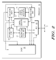
- FIG. 2 Illustrated in FIG. 2 is a portion of processor 14 which further details the control circuitry within processor 14 between cache 28 and a bus interface unit (BIU) 48 . Elements which are common with those of FIG. 1 are numbered the same in FIG. 2 .
- BIU 48 is connected to system interconnect bus 12 and to cache 28 as previously described.
- a second input/output terminal of BIU 48 is connected to a fifth input/output terminal of cache 28 and to a first input/output terminal of instruction fetch unit 27 .
- a third input/output terminal of BIU 48 is connected to a first input/output terminal of control circuitry 17 .
- a fourth input/output terminal of BIU 48 is connected to a sixth input/output terminal of cache 28 and to a first input/output terminal of a load/store unit 33 .
- a second input/output terminal of the instruction fetch unit 27 is connected to a first input/output terminal of an instruction pipe or instruction pipeline 23 .
- a second input/output terminal of instruction pipeline 23 is connected to a first input/output terminal of execution units 25 .
- Execution units 25 generally include units such as a floating point unit, an integer unit and other processing units.
- a third input/output terminal of instruction pipeline 23 is connected to a second input/output terminal of control circuitry 17 .
- a third input/output terminal of instruction fetch unit 27 is connected to a third input/output terminal of control circuitry 17 .
- a fourth input/output terminal of cache 28 is connected to a fourth input/output terminal of control circuitry 17 .
- a fifth input/output terminal of control circuitry 17 is connected to a second input/output terminal of execution units 25 .
- a third input/output terminal of execution units 25 is connected to the second input/output terminal of cache 28 .
- a fourth input/output terminal of execution units 25 is connected to a first input/output terminal of general purpose registers (GPRs) 31 .
- a second input/output terminal of general purpose registers 31 is connected to a second input/output terminal of load/store unit 33 .
- a third input/output terminal of load/store unit 33 is connected to the second input/output terminal of instruction pipeline 23 and to the first input/output terminal of execution units 25 .
- a fourth input/output terminal of load/store unit 33 is connected to a sixth input/output terminal of control circuitry 17 .
- control circuitry 17 of processor 14 functions to control and coordinate BIU 48 and cache 28 operations as well as the instruction fetch, decode and various execution units of processor 14 .
- instructions are coupled via BIU 48 or cache 28 into the instruction fetch unit 27 and placed in the instruction pipeline 23 .
- the instructions are executed by execution units 25 and results are stored off in GPRs 31 .
- Load/store unit 33 operates under control of control circuitry 17 to load information needed for processing by execution units 25 from and to store information from GPRs 31 to cache 28 and/or system interconnect bus 12 . Therefore, the portion of processor 14 detailed in FIG. 2 illustrates the instruction execution operation of processor 14 separate from the cache coherency management function. Various alternate embodiments of processor 14 may be implemented as well.
- FIG. 3 Illustrated in FIG. 3 is further detail of a portion of processor 14 which further details cache 28 and associated cache snooping circuitry, in accordance with one embodiment of the present invention.
- BIU 48 has a first input/output terminal connected via a bidirectional multiple-bit conductor to system interconnect bus 12 .
- Processing circuitry 40 of processor 14 has a first output that is connected to an input of BIU 48 .
- a second input/output terminal of BIU 48 is connected to a first input/output terminal of cache 28 .
- a second input/output terminal of cache 28 is connected via a bidirectional multiple-bit conductor to a first input/output terminal of processing circuitry 40 .
- a third input/output terminal of cache 28 is connected via a bidirectional multiple-bit conductor to a first input/output terminal of an arbiter 42 .
- a fourth input/output terminal of cache 28 is connected to a first input/output terminal of snoop control 54 .
- a second output of processing circuitry 40 is connected to a first input of arbiter 42 for providing an access address.
- a second input/output terminal of processing circuitry 40 is connected to a second input/output terminal of arbiter 42 .
- Snoop control 54 has a second input/output terminal connected to a third input/output terminal of the arbiter 42 .
- a third input/output terminal of snoop control 54 is connected to a third input/output terminal of processing circuitry 40 .
- An output of snoop control 54 provides a snoop status signal, and an input of snoop control 54 receives a snoop request signal, both of which may be considered part of the snoop control interface.
- Snoop queue circuitry 44 has a first output connected to a second input of arbiter 42 for providing a snoop address from the stored (N+1) entries.
- a second output of snoop queue circuitry 44 is connected to a third input of the arbiter 42 for providing status information associated with each snoop address. This status information may be provided to indicate that the current snoop address is valid and that a request for snoop lookup to arbiter 42 is valid.
- a fourth input/output terminal of the arbiter 42 is connected to a first input/output terminal of snoop queue circuitry 44 for providing access control. This access control is used to handshake snoop requests and snoop grants and coordinates the operation of the snoop queue circuitry 44 .
- a fourth input/output terminal of snoop control 54 is connected to a second input/output terminal of snoop queue circuitry 44 for providing snoop addresses and other snoop request information from the system interconnect 12 to the snoop queue circuitry 44 .
- a third output of snoop queue circuitry 44 is connected to a fourth input of arbiter 42 for providing a queue fullness indicator signal.
- Snoop queue circuitry 44 includes a snoop queue 46 coupled to queue fullness determination logic 45 .
- Processing circuitry 40 may include circuitry typically found in a processor such as e.g. an instruction pipe unit, execution units, an instruction fetch unit, control circuitry, general purpose registers, a load store unit, and a prefetch unit.
- processing circuitry 40 may include instruction pipe 23 , instruction fetch unit 27 , control circuitry 17 , execution units 25 , GPRs 31 , and load/store unit 33 , of FIG. 2 .
- Processors of other embodiments may include other types of circuitry.
- processing circuitry 40 executes instructions that generate requests for data to be read from system memory 20 (or other slave or I/O devices) and for data to be written to system memory 20 (or other slave or I/O devices).
- processing circuitry 40 will check cache 28 (via arbiter 42 ) to see if it has any data that corresponds to that system memory address. If not, load/store unit 33 of processing circuitry 40 may generate via BIU 48 a transaction on system interconnect bus 12 to request data from memory 20 at that system address.
- the system memory 20 will provide the requested data on system interconnect bus 12 to processor 14 where BIU 48 receives the data and provides the data to processing circuitry 40 and to cache 28 in some embodiments.
- BIU 48 receives the data and provides the data to processing circuitry 40 and to cache 28 in some embodiments.
- the transaction is completed.
- Write transactions to memory 20 can be initiated by processor 14 where a write address and data are provided on interconnect bus 12 to be written to memory 20 at the address, and may also be written to cache 28 . Also, data may be written to or read from other slave devices 24 and I/O devices 26 of data processing system 10 in other embodiments.
- Cache 28 may be an instruction cache, a data cache, or a combination of the two.
- data herein in regards to a transaction may refer to the information stored in either an instruction cache or a data cache.
- Processor 14 also includes circuitry for snoop request management.
- the snoop request circuitry operates to keep the data in cache 28 coherent with other copies of the data stored in memory 20 and other caches of data processing system 10 .
- Snoop control 54 receives snoop requests from cache coherency manager 18 via the snoop control interface.
- Processor 14 includes snoop queue circuitry 44 including snoop queue 46 for storing snoop requests received from the snoop control interface.
- snoop request queue 46 may be implemented as a first-in first-out buffer (FIFO).
- the FIFO may be implemented as a circular buffer.
- snoop request queue 46 Within snoop request queue 46 is a plurality of (N+1) entries where N is an integer. Each entry in snoop request queue 46 has an address field and a status field that includes status information. The address field stores the address of the transaction for which a snoop request was generated. In the embodiment shown, a first status bit is a valid (V) bit which indicates whether the entry in snoop request queue 46 is valid. Other types of status bits may be included in other embodiments. Each entry also includes a snoop request ID field that stores a snoop request ID for the snoop request generated by the cache coherency manager.
- queue fullness determination logic 45 is coupled to each entry of snoop request queue 46 so that it can determine a fullness of snoop request queue 46 .
- the fullness of snoop request queue 46 is a measure of how many valid snoop requests are currently present in snoop request queue 46 . Therefore, in the illustrated embodiment, queue fullness determination logic 45 provides a queue fullness indicator to arbiter 42 which indicates how full snoop request queue 46 is.
- snoop control 54 and snoop queue circuitry 44 operate to keep cache 28 coherent with other copies of the information in system 10 .
- Snoop control 54 receives a snoop request from cache coherency manager 18 via the snoop control interface and provides the address of the snoop request, along with the request ID to be stored in snoop request queue 46 . Therefore, in one embodiment, cache coherency manager 18 may be characterized as detecting possible incoherencies caused by at least one transaction between a processor and system memory 20 or within a processor and a cache. The snoop requests provided by cache coherency manager 18 to snoop control 54 may therefore arise from these possible incoherencies. In an alternate embodiment, the functionality of cache coherency manager 18 may be distributed within the different masters of system 10 . For example, the functions may be performed within each of the processors 14 - 16 .
- Arbiter 42 arbitrates access to cache 28 between the processing circuitry 40 and snoop queue circuitry 44 in an efficient manner to minimize the time that processing circuitry 40 does not have access to cache 28 . This minimization may be accomplished in one embodiment, by performing arbitration based on idle cycles of processing circuitry 40 or based on idle cycles as well as a fullness of snoop request queue 46 , as will be discussed further below and with respect to FIG. 4 .
- snoop control 54 When a snoop request is received by snoop control 54 , snoop control 54 routes the snoop address to the snoop queue circuitry 44 .
- Various embodiments of the function of snoop queue circuitry 44 may be implemented.
- all received snoop addresses from snoop control 54 are stored in snoop request queue 46 .
- arbiter 42 provides snoop queue circuitry 44 with access to cache 28 , access addresses from the processing circuitry 40 are not permitted to cache 28 via arbiter 42 .
- arbiter 42 provides the snoop addresses from snoop request queue 46 to cache 28 for searching (i.e. for performing a snoop lookup operation).
- the snoop addresses are removed from the snoop request queue 46 on a first-in, first-out (FIFO) basis.
- snoop queue circuitry 44 When a snoop address is present in snoop request queue 46 , snoop queue circuitry 44 signals arbiter 42 to request arbiter 42 to arbitrate for access to cache 28 .
- cache 28 has a single set of address tags and therefore must be either be dedicated to the processor (i.e. processing circuitry 40 ) for addressing or to snoop queue circuitry 44 for addressing.
- arbiter 42 prevents access by processing circuitry 40 to cache 28
- snoop addresses from circuitry 44 are routed through arbiter 42 to cache 28 .
- Circuitry within cache 28 performs a snoop look-up operation. The snoop-lookup operation includes comparing the snoop address with all the addresses presently stored in cache 28 .
- snoop control 54 may signal arbiter 42 to arbitrate for access to cache 28 .
- arbiter 42 arbitrates access to cache 28 between access addresses from processing circuitry 40 and snoop addresses from snoop queue circuitry 44 .
- processing circuitry 40 may signal to arbiter 42 for the need to access cache 28 by simply providing an access address to arbiter 42 , which operates as a processing circuitry request for access to cache 28 .
- a separate processing circuitry request signal may be provided from processing circuitry 40 to arbiter 42 to request access to cache 28 for a current access address.
- snoop queue circuitry 44 may signal to arbiter 42 for the need to access cache 28 by simply providing a snoop address to arbiter 42 .
- a separate snoop circuitry access request signal may be provided from snoop queue circuitry 44 to arbiter 42 to request access to cache 28 for a current snoop address corresponding to a next snoop request in snoop request queue 46 .
- arbiter 42 selects priority between an access address and a snoop address for accessing cache 28 based on idle cycles of processing circuitry 40 and on a fullness of snoop request queue 46 .
- arbiter 42 using the queue fullness signal from queue fullness determination logic 45 , determines whether or not fullness of queue 46 exceeds a predetermined fullness threshold. In one embodiment, this determination is made by threshold control circuitry 41 within arbiter 42 .
- the fullness threshold may be stored within threshold control circuitry 41 or anywhere within system 10 . In one embodiment, the fullness threshold is programmable such that it may be dynamically changed during operation of processor 14 .
- arbiter 42 grants access to the snoop address, thus providing the snoop address corresponding to a next snoop request from the queue 46 to cache 28 such that a snoop look-up operation based on that next snoop request can be performed.
- arbiter 42 may wait to perform a snoop look-up operation for a next snoop request in queue 46 until an idle access request cycle occurs from processing circuitry 40 to cache 28 occurs.
- snoop addresses corresponding to snoop requests stored in queue 46 are only processed (i.e. provided to cache 28 for a snoop look-up operation) if there is an idle access request cycle from processing circuitry 40 .
- snoop look-up operations do not hinder the efficiency of processing circuitry 40 , unless queue 46 has reached a certain level of fullness. Operation of arbiter 42 will be discussed in further detail with respect to the timing diagram of FIG. 4 below.
- arbiter 42 may not base its decision on the fullness of queue 46 and may always wait for an idle access request cycle from processing circuitry 40 for allowing access of a snoop address to cache 28 .
- an idle access request cycle (or an idle cycle) may refer to any clock cycle in which processing circuitry 40 does not have a pending access address requiring access to cache 28 .
- An active cycle may refer to any clock cycle in which processing circuitry 40 requires access to cache 28 , or to any clock cycle which is not considered an idle cycle.
- the snoop control interface includes a snoop request signal interface and a snoop status signal interface.
- a snoop acknowledgement signal interface may be included, such as, for example, a snoop acknowledgement signal interface, a snoop error signal interface, etc.
- the snoop request signal interface includes a request signal line for indicating that a snoop request is being made, a snoop command line indicating the type of bus transaction that generated the snoop, a snoop address line which is the address of the transaction being snooped, and a snoop request ID line, which is a number generated by the cache coherency manager identifying the snoop request.
- These signal lines may be multi-bit (either in parallel or serial in some embodiments) or single bit in some embodiments.
- the snoop status signal interface is used to indicate to the cache coherency manager 18 that a snoop request has been processed by the cache and the result of the cache snoop (e.g. whether an entry for the data address was found in the cache or not or whether an error (parity or other error type) was found with the data of the entry).
- the snoop status interface includes a snoop response line and a snoop request ID line indicating the ID number of the snoop request. These lines may be multi-bit as well.
- system 10 may include processors of other configurations and/or that perform transactions and snoop operations in a different manner.
- a processor may have other circuitry not shown in FIG. 3 or may not include all of the circuitry shown in FIG. 3 .
- a processor may include other circuitry for handling snoop requests in another manner as well, rather than by invalidation of matching cache entries.
- FIG. 4 illustrates, in timing diagram form, operation of a portion of the circuitry of FIG. 3 , in accordance with one embodiment of the present invention.
- the fullness threshold is set to 2.
- the priority selection by arbiter 42 selects the snoop address provided by snoop queue circuitry 44 (assuming there is a valid snoop request in queue 46 ) to arbiter 42 to provide to cache 28 . If there was a valid snoop request in queue 46 , this snoop request is processed by cache 28 since arbiter 42 selects the snoop address for provision to cache 28 .
- processing circuitry 14 makes a processing circuitry request, requesting access to cache 28 in the next cycle. That is, as discussed above, processing circuitry 14 may provide an access address to arbiter 42 , which operates as the processing circuitry request, or may provide a separate request signal to arbiter 42 . Also, later in cycle 1 , a snoop request is received via snoop control interface by snoop control 54 for storage into snoop request queue 46 .
- a processing circuitry request since a processing circuitry request is present for cycle 2 , it is not an idle cycle. Furthermore, at the start of cycle 2 , queue 46 included no snoop requests; therefore queue 46 has not yet exceeded the fullness threshold. In cycle 2 , arbiter 42 selects the access address from processing circuitry 40 as having priority and thus provides this access address to cache 28 . Also, in cycle 2 , the snoop request remains asserted indicating that another snoop request is received in cycle 2 . This snoop request is received by snoop control 54 and stored into queue 46 at the beginning of cycle 3 .
- arbiter 42 selects the snoop address corresponding to the next snoop request to be processed from queue 46 to provide to cache 28 during this idle cycle.
- cycle 4 both a processing circuitry request is present and a snoop address from queue 46 is available. However, since queue 46 has not exceeded the fullness threshold of 2, arbiter 42 selects the access address corresponding to the processing circuitry request to provide to cache 28 . However, since in cycle 4 , the snoop request from cycle 3 is placed in queue 46 , the fullness of queue 46 increases (i.e. transitions) to 2.
- cycle 5 both a processing circuitry request is present and a snoop address from queue 46 is available.
- queue 46 has not yet exceeded the fullness threshold of 2. Therefore, arbiter 42 again selects the access address corresponding to the processing circuitry request to provide to cache 28 .
- a snoop request is again loaded into queue 46 at the beginning of cycle 5 due to the asserted snoop request in cycle 4 , therefore, the fullness of queue 46 transitions to 3 in cycle 5 , which does exceed the fullness threshold of 2.
- cycle 5 although a processing circuitry request is present for cycle 6 , and thus is an active cycle, the fullness of queue 46 has exceeded the fullness threshold of 2. Therefore, arbiter 42 selects the snoop address corresponding to a next snoop request to be processed from queue 46 to provide to cache 28 for a snoop look-up operation in cycle 6 . Since both a snoop request is processed from queue 46 and a new snoop request for storage into queue 46 is again received, in cycle 6 , the fullness of queue 46 remains at 3, which still exceeds the fullness threshold of 2. Later in cycle 6 , the snoop request is negated, indicating that a snoop request is not being received by snoop control 54 .
- cycle 6 there is still a processing circuitry request present and thus is an active cycle; however, the fullness of queue 46 still exceeds the fullness threshold of 2. Therefore, arbiter 42 selects the snoop address corresponding to a next snoop request to be processed from queue 46 to provide to cache 28 for a snoop look-up operation in cycle 7 .
- a snoop request is processed from queue 46 but no new snoop request is received by snoop control 54 ; therefore, the fullness of queue 46 transitions down to 2, which no longer exceeds the fullness threshold.
- arbiter 42 selects the access address corresponding to the processing circuitry request to provide to cache 28 for a lookup in cycle 8 . Since no snoop request is received in cycle 7 , the fullness of queue 46 remains at 2.
- a request between processor 14 (e.g. processing circuitry 40 ) and cache 28 can be detected by arbiter 42 , where arbiter 42 can provide a snoop address to cache 28 for a snoop look-up operation if the detected request corresponds to an idle request (i.e. corresponds to an idle cycle with no access address present) and not provide the snoop address to cache 28 if the request is a processing circuitry request with a corresponding access address.
- arbiter 42 may provide the access address to cache 28 and then provide the snoop address to cache 28 if a next request detected between processing circuitry 40 and cache 28 is an idle request (i.e. corresponds to an idle cycle with no access address present).
- arbiter 42 can bias priority for access to cache 28 towards processing circuitry 40 , so as not to negatively impact the performance of processor 14 , while still ensuring that the snoop queue circuitry 44 does not stall operation due to an overflow in queue 46 .
- efficiency of processor 14 may be improved.
- snoop look-up operations to be performed once a certain number of snoop requests are pending, regardless of whether there is an idle or active cycle, stalls due to an overflow of snoop requests may also be avoided.
- FIG. 5 illustrates a block diagram of a portion of an arbiter 142 which may be used as arbiter 42 of FIG. 3 . That is, arbiter 142 operates the same as arbiter 42 with the addition of the elements illustrated in FIG. 5 ; therefore, except to the extent described differently in reference to FIGS. 5 and 6 , the descriptions provided above with respect to arbiter 42 also apply to arbiter 142 . That is, arbiter 142 may be the same as arbiter 42 but with additional capabilities.
- the portion of arbiter 142 illustrated in FIG. 5 includes a snoop starvation counter 144 (also referred to as Smax counter 144 ), a processing circuitry starvation counter 146 (also referred to as Pmax counter 146 ), and priority inversion logic 148 .
- the starvation counters may be used to prevent starvation of either pending accesses from processing circuitry 40 or of pending snoop requests from snoop queue 46 from accessing cache 28 .
- counter 146 keeps track of the number of cycles an access address from processing circuitry 40 has been pending because it is unable to gain access to cache 28 due to arbiter 142 selecting snoop addresses from snoop queue 46 to provide to cache 28 (which, in the case of both an access address pending from processing circuitry 40 and a snoop address pending from snoop queue 46 , occurs when the queue fullness is at or above the fullness threshold level, in accordance with the lazy protocol described above).
- counter 146 is set to a maximum value, Pmax, the first time a pending access address from processing circuitry 40 is not granted access to cache 28 by arbiter 142 .
- counter 146 For each subsequent cycle that this access address is still pending (still waiting to be granted access to cache 28 ), counter 146 is decremented. When counter 146 expires, arbiter 142 will grant priority to the pending access address from processing circuitry 40 for a predetermined number of cycles, thus preempting any valid snoop requests from snoop queue 46 . In one embodiment, the predetermined number of cycles is only one cycle. In one embodiment, counter 146 may be reloaded with Pmax whenever a pending access address from processing circuitry 40 is granted access to cache 28 by arbiter 142 .
- priority inversion logic 148 can monitor counter 146 to determine when it has expired, and, in response thereto, cause arbiter 142 to invert the priority to select the pending access address for one or more cycles (even though the queue fullness of snoop queue 46 is at or above the fullness threshold level). In this manner, an access request from processing circuitry 40 may be performed (i.e. provided to cache 28 ) in response to a consecutive number of snoop look-up operations exceeding a limit (e.g. Pmax).
- a limit e.g. Pmax
- each time counter 146 is decremented it can be assumed that a snoop look-up operation is performed (where the snoop look-up operation is performed in response to the snoop request which was provided to cache 28 ).
- counter 144 keeps track of the number of cycles a valid snoop address from snoop queue 46 has been pending because it is unable to gain access to cache 28 due to arbiter 142 selecting access addresses from processing circuitry 40 to provide to cache 28 (which, in the case of both an access address pending from processing circuitry 40 and a snoop address pending from snoop queue 46 , occurs when the queue fullness is below the fullness threshold level, in accordance with the lazy protocol described above).
- counter 144 is set to a maximum value, Smax, the first time a valid snoop request (i.e. a pending snoop request) from snoop queue is not granted access to cache 28 by arbiter 142 .
- counter 144 For each subsequent cycle that this snoop request remains pending (still waiting to be granted access to cache 28 by arbiter 142 ), counter 144 is decremented. When counter 144 expires, arbiter 142 will grant priority to the pending snoop address from snoop queue 46 for a predetermined number of cycles, thus preempting any pending access addresses by processing circuitry 40 . In one embodiment, the predetermined number of cycles is only one cycle. Counter 144 may be reloaded with Smax whenever a pending snoop address from snoop queue 46 is granted access to cache 28 by arbiter 142 .
- priority inversion logic 148 can monitor counter 144 to determine when it has expired, and, in response thereto, cause arbiter 142 to invert the priority to select the pending snoop request for one or more cycles (even though the queue fullness of snoop queue 46 is below the fullness threshold level).
- a pending snoop request from snoop queue 46 may be processed (i.e. provided to cache 28 ) in response to a consecutive number of access addresses from processing circuitry 40 (i.e. processor requests) being processed exceeding a limit (e.g. Smax). That is, in one embodiment, such as when cache operations are pipelined, each time counter 144 is decremented, it can be assumed that an access address from processing circuitry 40 is processed (where the access address is processed by being provided to cache 28 ).
- arbiter 142 may further use the starvation counters, in addition to the fullness of snoop queue 46 , to arbitrate this contention. That is, if both an access address and a snoop address are pending and the snoop queue fullness is at or greater than the fullness threshold, arbiter 142 , based on the expiration of starvation counter 146 (i.e. based on Pmax) may select the pending access address and thus pre-empt the pending snoop address.
- arbiter 142 may select the pending snoop address and thus pre-empt the pending access address. This may ensure that snoop queue 46 does not hold a snoop request for an unbounded time and may likewise ensure that processing circuitry 40 can make forward progress when overloaded with snoop queue traffic requests.
- counters 144 and 146 may be cleared to zero and incremented for each subsequent cycle the corresponding access address or snoop address remains pending until the value of Pmax or Smax, respectively, is reached in order to invert the priority.
- FIG. 6 illustrates a timing diagram which describes operation of a portion of FIG. 3 along with the portion of arbiter 142 of FIG. 5 in accordance with one embodiment.
- the Pmax counter signal illustrated in FIG. 6 when the Pmax counter signal illustrated in FIG. 6 is asserted, it indicates that counter 146 is counting (e.g. decrementing) and when the Smax counter signal is asserted, it indicates that counter 144 is counting (e.g. decrementing).
- the Pmax counter signal illustrated in FIG. 6 when the Pmax counter signal illustrated in FIG. 6 is asserted, it indicates that counter 146 is counting (e.g. decrementing) and when the Smax counter signal is asserted, it indicates that counter 144 is counting (e.g. decrementing).
- the Smax counter signal when the Smax counter signal is asserted, it indicates that counter 144 is counting (e.g. decrementing).
- it in each cycle in which counter 146 or 144 is not counting (e.g. decrement
- arbiter 142 grants access to the pending snoop address (as indicated by the assertion of PRI for one cycle), thus pre-empting the next pending access address from processing circuitry 40 (since the queue fullness would typically indicate that priority should be granted to the pending access address from processing circuitry 40 ).
- counter 146 may be loaded with Pmax. However, in the current embodiment, priority is inverted for only one cycle, therefore, in cycle 6 , priority is returned to processing circuitry 40 (as indicated by the negation of PRI). Note that again, in cycle 10 , priority is inverted for one cycle from processing circuitry 40 to snoop queue 46 . In this manner, snoop queue 46 is not completely starved during the contention of pending processing circuitry requests and pending snoop requests.
- arbiter 142 grants priority to the snoop address from snoop queue 46 .
- counter 146 is loaded with Pmax and decremented for each cycle for which access to cache 28 is denied to the pending processing circuitry request. Therefore, counter 146 is decremented in each of cycles 13 - 15 , at which point it expires. Therefore, note that in cycle 16 , priority is given to the pending processing circuitry request, thus preempting the pending snoop address from snoop queue 46 .
- cycle 16 since priority is granted to the access address and thus the pending snoop address from snoop queue 46 is denied access to cache 28 , counter 144 may be loaded with Smax. However, in the current embodiment, priority is inverted for only one cycle, therefore, in cycle 17 , priority is returned to snoop queue 46 (as indicated by the assertion of PRI). In this manner, processing circuitry 40 is also not completely starved during the contention of pending processing circuitry requests and pending snoop requests.
- the values of Pmax and Smax used in the embodiment of FIGS. 5 and 6 can be hardwired values or programmable. In one embodiment, they may be dynamically changed in response to operation of system 10 . For example, in one embodiment, based on information provided by system monitor 13 , such as performance or throughput information, the values of Pmax or Smax or both can dynamically be changed, in order to attempt to optimize a level of snoop or processor throughput or performance.
- FIG. 7 illustrates a block diagram of a portion of an arbiter 242 which may be used as arbiter 42 of FIG. 3 . That is, arbiter 242 operates the same as arbiter 42 with the addition of the elements illustrated in FIG. 7 ; therefore, except to the extent described differently in reference to FIGS. 7 and 8 , the descriptions provided above with respect to arbiter 42 also apply to arbiter 242 . That is, arbiter 242 may be the same as arbiter 42 but with additional capabilities.
- a counter mechanism may be used to help ensure that neither processing circuitry 40 or snoop queue 46 is starved from being able to access cache 28 .
- a single counter, counter 252 may be used to prevent starvation of either processing circuitry 40 or snoop queue 46 .
- counter 252 counts down (i.e. is decremented) when either an access address from processing circuitry 40 or a snoop address from snoop queue 46 is blocked (i.e. denied access to cache 28 ).
- the current priority (indicated again by PRI) is inverted for a predetermined number of cycles to allow the other lower priority requester to access cache 28 .
- the current priority is inverted for one cycle (i.e. one access slot).
- counter 252 Upon expiration of counter 252 , it is reloaded with a value that is dependent on the fullness of snoop queue 46 .
- counter 252 is reloaded with a counter value selected from one of two values, Pmax and Smax, which may correspond to two effective modalities of snoop traffic.
- Pmax may be loaded when there are heavy bursts of dense snoop traffic (meaning snoop queue 46 is more full and thus often at or above the fullness threshold), and Smax may be loaded when there is less dense snoop request traffic (such as when the fullness of snoop queue 46 is often below the fullness threshold). Therefore, in one embodiment, when reloading counter 252 , a load value is selected between Pmax and Smax based on the fullness of snoop queue 46 in comparison with the fullness threshold. Note that the values of Pmax and Smax provide boundaries, i.e.
- snoop queue 46 may therefore ensure that snoop queue 46 does not hold a snoop request for an unbounded time and may likewise ensure that processing circuitry 40 can make forward progress when overloaded with snoop queue traffic requests.
- the values of Pmax and Smax used in the embodiment of FIGS. 7 and 8 can be hardwired values or programmable. In one embodiment, they may be dynamically changed in response to operation of system 10 . For example, in one embodiment, based on information provided by system monitor 13 , such as performance or throughput information, the values of Pmax or Smax or both can dynamically be changed, in order to achieve a particular system metric, such as latency or throughput.
- Arbiter 242 includes counter 252 , storage circuitry 244 for storing a Pmax value, storage circuitry 246 for storing an Smax value, multiplexers (MUXes) 250 and 254 , storage element 256 , and inverter 258 .
- a first data input of MUX 250 receives Pmax from storage circuitry 244 and a second data input of MUX 250 receives Smax from storage circuitry 246 .
- a control input of MUX 250 receives a count value select signal 248 which selects one of the two data inputs of MUX 250 to provide at its data output based on whether the fullness of snoop queue 46 is at or above the fullness threshold or not.
- the data output of MUX 250 is provided as the load value to counter 252 at its data input.
- the load enable (ld_en) and count enable (cnt_en) inputs of counter 252 will be described in more detail below.
- a zero detection output of counter 252 (which, when asserted, indicates that counter 252 has expired or reached zero), is provided as the control input of MUX 254 .
- MUX 254 receives an output of inverter 258 at a first data input, and receives an indication of whether “the fullness of snoop queue 46 is at or above the fullness threshold or there is no access address pending” at a second data input, and provides PRI at its data output.
- the data output of MUX 254 i.e. the current PRI
- PRI′ is provided at the input of inverter 258 .
- ” is a logical OR
- a “+” is also a logical OR
- a “&” is a logical AND
- a “ ⁇ ” is a logical NOT
- proc_pend when asserted, indicates that an access address (i.e. a processing circuitry request) from processing circuitry 40 is pending
- snp_pend when asserted, indicates than a snoop address (i.e. a snoop request) from snoop queue 46 is pending.
- MUX 250 selects whether Pmax or Smax should be loaded into counter 252 based on whether or not the fullness of snoop queue 46 is at or above the fullness threshold or not.
- ⁇ PRI′ is the inversion of the previous value of PRI (where the previous value of PRI is indicated as PRI′ and was stored in storage element 256 ).
- MUX 254 , storage element 256 , and inverter 258 operate to invert the priority for one cycle.
- cnt_en ((PRI & proc_pend)
- cnt_en 1) when a snoop address from snoop queue 46 has priority while there is a pending access address from processing circuitry 40 (i.e. “PRI & proc_pend”) or when an access address from processing circuitry 40 has priority while there is a pending snoop address from snoop queue 46 (i.e. “ ⁇ PRI & snp_pend”), and the priority has not just changed or toggled (i.e. “ ⁇ (PRI XOR PRI′)”). Therefore, counting is enabled when the priority has not changed and arbiter 142 had to resolve a contention by prioritizing an access request from one source over an access request from another source. If the counting is not enabled (i.e.
- MUX 254 , storage element 256 and inverter 258 allows for priority inversion by monitoring counter 252 to determine when it has expired, and, in response thereto, cause arbiter 242 to invert the priority to select the pending access address for one cycle when a consecutive number of snoop look-up operations exceeds a limit, such as Pmax (even though the queue fullness of snoop queue 46 is at or above the fullness threshold level) or invert the priority to select the pending snoop request for one cycle when a consecutive number of access addresses from processing circuitry 40 being processed exceeds a limit, such as Smax (even though the queue fullness of snoop queue 46 is below the fullness threshold level).
- Pmax even though the queue fullness of snoop queue 46 is at or above the fullness threshold level
- Smax even though the queue fullness of snoop queue 46 is below the fullness threshold level
- Pmax may represent the maximum number of cycles that processing circuitry 40 is to be denied access to cache 28
- Smax may represent the maximum number of cycles that snoop queue 46 is to be denied access to cache 28 .
- a single counter 252 may be used to ensure that neither requester is starved.
- Pmax to have a value of 1
- Smax to have a value of 0
- a round robin effect results for granting priority between access addresses and snoop addresses.
- FIG. 8 illustrates a timing diagram which describes operation of a portion of FIG. 3 along with the portion of arbiter 242 of FIG. 7 in accordance with one embodiment.
- Smax has a value of 3
- Pmax has a value of 2
- the fullness threshold has a value of 2.
- counter 252 is loaded with the value of Smax (where ld_en is asserted in cycle 1 ).
- PRI is negated to indicate that priority is granted to the pending access address since the queue fullness is below the fullness threshold and no starvation-preventing priority inversion occurs (since counter 252 has not expired).
- cycle 2 the queue fullness transitions (indicated by “ ⁇ ”) to 1 due to a snoop request which was received for storage into snoop queue 46 in cycle 1 (such as from cache coherency manager 18 ), as indicated by the assertion of “snoop request for storage to snoop queue” in cycle 1 .
- Counter 252 is reloaded with the value of Smax at the beginning of cycle 2 .
- PRI remains negated to grant priority to the next pending access address (whose existence is indicated by the processing circuitry request remaining asserted in cycle 2 ).
- cycle 3 the queue fullness transitions to 2 due to the snoop request for storage to snoop queue 46 received in cycle 2 . Therefore, in cycle 3 , the queue fullness is at or above the fullness threshold of 2. Therefore, PRI is asserted to grant priority to the snoop address (i.e. the snoop request pending from snoop queue 46 ), in accordance with the lazy snoop protocol described above.
- Counter 252 is decremented at the beginning of cycle 3 to a value of 2 since a snoop queue request is still pending and an access request was performed to cache 28 in cycle 3 .
- counter 252 is enabled to be reloaded at the beginning of cycle 4 .
- cycle 4 it is reloaded with Pmax rather than Smax since the queue fullness is now at or above the fullness threshold (as indicated by assertion of the threshold comparison result).
- cycle 4 the queue fullness remains at or above the fullness threshold (due to another incoming snoop request for storage into snoop queue 46 received in cycle 3 ).
- Ld_en is negated since processing circuitry 40 is again denied access to cache 28 (since PRI is asserted), thus counter 252 will be decremented from 2 (Pmax) to 1 at the beginning of cycle 5 . Since counter 252 has not expired, PRI remains asserted to grant priority to the snoop address.
- cycle 5 the processing circuitry request is negated, indicating that there is no pending access address to be processed. Thus, cycle 5 is considered an idle request cycle from processing circuitry 40 .
- PRI remains asserted in cycle 5
- counter 252 is enabled to be loaded at the beginning of cycle 6 since there is no access request from processing circuitry 40 , and PRI remains asserted.
- no new snoop request for storage into snoop queue was received in cycle 5 and a snoop request pending from snoop queue was processed in cycle 5 , thus the queue fullness transitions down to 1, which is below the threshold.
- PRI remains asserted, in accordance with the lazy snoop protocol described above. Since the threshold is not exceeded, Smax is selected to be loaded into the counter at the beginning of cycle 6 .
- cycle 6 the queue fullness remains at 1 due to the additional snoop request for storage into snoop queue 46 received in cycle 5 and due to a snoop request being processing in cycle 5 .
- a pending access address i.e. processing circuitry request is again asserted
- PRI is negated to grant priority to the pending access address.
- counter 252 is loaded with Smax. In each of cycles 7 - 9 , PRI remains negated to consecutively grant priority to the pending access addresses, thus denying access to cache 28 by snoop queue 46 .
- cycle 11 the fullness of snoop queue 46 transitions to 0. Also in cycle 11 , PRI is again negated to revert priority back to the pending access address and counter 252 is enabled to be reloaded with Smax again (since there is no snoop request pending) at the beginning of cycle 12 .
- cycle 12 the queue fullness transitions to 1 due to the snoop request for storage into snoop queue 46 received in cycle 11 .
- PRI remains negated since the queue fullness is still below the fullness threshold (as indicated by the negated threshold comparison result).
- counter 252 is being reloaded with Smax, since there is no snoop request pending.
- cycle 13 the queue fullness transition to 2 due to the snoop request for storage into snoop queue 46 received in cycle 12 , and thus, since a queue fullness of 2 is at or above the fullness threshold, PRI is asserted to grant priority to the snoop address (to the snoop request pending from snoop queue 46 ).
- cycle 13 is a first cycle in which the pending access address from processing circuitry 40 is denied access to cache 28 and the queue fullness is at or above the fullness threshold (indicated by the assertion of the threshold comparison result)
- counter 252 will be loaded with Pmax at the beginning of cycle 14 .
- the queue fullness remains at 2 (which is at or above the fullness threshold), and thus PRI remains asserted giving priority to the snoop requests.
- counter 252 is decremented.
- PRI is negated for one cycle to grant priority to a pending access address from processing circuitry 40 , even though the queue fullness remains at or above the fullness threshold.
- This starvation-preventing priority inversion pre-empts the pending snoop request from snoop queue 46 .
- PRI is again asserted to revert priority back to the pending snoop request and counter 252 is reloaded with Pmax again (since the queue fullness is still at or above the fullness threshold).
- counter 252 is again reloaded with either Smax or Pmax, based on the fullness of snoop queue 46 .
- priority inversion is performed for one cycle (or more cycles, in alternate embodiments) in order to prevent starvation. In this case, upon reverting priority back to the previous priority, counter 252 is also reloaded to begin the count down again.
- counter 252 when priority is granted to pending snoop requests from snoop queue 46 due to the lazy protocol (because the queue fullness is at or above the fullness threshold or there is an idle cycle), counter 252 is loaded with Pmax and counts the number of cycles that processing circuitry 40 is denied access to cache 28 (i.e. in order to count the number of consecutive snoop look-up operations performed) such that processing circuitry 40 is not continuously starved.
- counter 252 is loaded with Smax and counts the number of cycles that snoop queue 46 is denied access to cache 28 (i.e.
- snoop queue 46 in order to count the number of consecutive access addresses that are processed) such that snoop queue 46 is not continuously starved.
- Pmax is less than Smax such that processing circuitry 40 is guaranteed to be starved less than snoop queue 46 .
- the starvation-preventing priority inversion can be performed for more than one cycle or can be performed for a different number of cycles depending on which requestor the priority is inverting to.
- FIG. 1 and the discussion thereof describe an exemplary memory system architecture
- this exemplary architecture is presented merely to provide a useful reference in discussing various aspects of the invention.
- the description of the architecture has been simplified for purposes of discussion, and it is just one of many different types of appropriate architectures that may be used in accordance with the invention.
- Those skilled in the art will recognize that the boundaries between logic blocks are merely illustrative and that alternative embodiments may merge logic blocks or circuit elements or impose an alternate decomposition of functionality upon various logic blocks or circuit elements.
- any two components herein combined to achieve a particular functionality can be seen as “associated with” each other such that the desired functionality is achieved, irrespective of architectures or intermedial components.
- any two components so associated can also be viewed as being “operably connected,” or “operably coupled,” to each other to achieve the desired functionality.
- the computer readable media may include, for example and without limitation, any number of the following: magnetic storage media including disk and tape storage media; optical storage media such as compact disk media (e.g., CD-ROM, CD-R, etc.) and digital video disk storage media; nonvolatile memory storage media including semiconductor-based memory units such as FLASH memory, EEPROM, EPROM, ROM; ferromagnetic digital memories; MRAM; volatile storage media including registers, buffers or caches, main memory, RAM, etc.; and data transmission media including computer networks, point-to-point telecommunication equipment, and carrier wave transmission media, just to name a few.
- magnetic storage media including disk and tape storage media
- optical storage media such as compact disk media (e.g., CD-ROM, CD-R, etc.) and digital video disk storage media
- nonvolatile memory storage media including semiconductor-based memory units such as FLASH memory, EEPROM, EPROM, ROM
- ferromagnetic digital memories such as FLASH memory, EEPROM, EPROM, ROM
- system 10 is implemented in a computer system such as a personal computer system.
- Computer systems are information handling systems which can be designed to give independent computing power to one or more users.
- Computer systems may be found in many forms including but not limited to mainframes, minicomputers, servers, workstations, personal computers, notepads, personal digital assistants, electronic games, automotive and other embedded systems, cell phones and various other wireless devices.
- a typical computer system includes at least one processing unit, associated memory and a number of input/output (I/O) devices.
- any type of memory cache synchronous or asynchronous
- Various types of memory circuits including dynamic random access memory (DRAM), synchronous random access memory (SRAM), magnetoresistive random access memory (MRAM), FLASH, shift registers and addressable storage registers may be used to implement the cache.
- DRAM dynamic random access memory
- SRAM synchronous random access memory
- MRAM magnetoresistive random access memory
- FLASH shift registers and addressable storage registers
- system interconnect or bus protocols could be implemented.
- system components in addition to those used in FIG. 1 may be provided.
- all circuitry described herein may be implemented either in silicon or another semiconductor material or alternatively by software code representation of silicon or another semiconductor material.
- Coupled is not intended to be limited to a direct coupling or a mechanical coupling.
- Item 1 includes a method of performing a snoop look-up operation in a system having a first cache and a first processor, wherein the first processor generates requests to the first cache for data.
- the method includes loading a snoop queue with snoop requests, wherein a fullness of the snoop queue is a measure of how many snoop requests are in the snoop queue; determining if the fullness of the snoop queue exceeds a predetermined threshold; performing a snoop look-up operation in the first cache if the fullness of the snoop queue exceeds the predetermined threshold, wherein the snoop look-up operation is based on a snoop request from the snoop queue corresponding to an entry in the snoop queue; and if the fullness of the snoop queue does not exceed the predetermined threshold and there is at least one snoop request in the snoop queue, waiting to perform a snoop look-up operation until
- Item 2 includes the method of item 1, wherein the step of loading is further characterized by the snoop requests arising from possible incoherencies, and the method further includes detecting possible incoherencies caused by at least one transaction between a second processor and a main memory or between the second processor and a second cache.
- Item 3 includes the method of item 2, wherein the step of detecting possible incoherencies is further characterized by using a coherency manager coupled to a system interconnect, and wherein the second processor and the main memory are coupled to the system interconnect.
- Item 4 includes the method of item 1 and further includes comprising informing a snoop control circuit of a result arising from performing the snoop look-up operation, wherein the snoop control circuit is part of the first processor or the first cache.
- Item 5 includes the method of item 1, wherein the step of performing the snoop look-up operation in the first cache includes determining if there is a hit in the first cache; if there is a hit in the first cache, setting a bit in a line in the first cache to indicate an invalid entry in the line in the first cache; and if there is not a hit in the first cache, not changing the first cache.
- Item 6 includes the method of item 1 and further includes changing the predetermined threshold in response to a signal.
- Item 7 includes the method of item 1, wherein the step of loading the snoop queue is further characterized by the snoop queue being within the first processor.
- Item 8 includes the method of item 1, and further includes removing an entry corresponding to the snoop request for which the snoop look-up operation was performed from the snoop queue.
- Item 9 includes a system which includes a first processing unit; a first cache coupled to the first processing unit; an arbiter coupled to the first cache and the first processing unit; a snoop queue coupled to the arbiter that stores snoop requests and provides an output indicating a fullness of the snoop queue; and a snoop control circuit coupled to the snoop queue that provides snoop requests to the snoop queue.
- the arbiter compares the output indicating the fullness of the snoop queue, detects if the first processing unit is performing an idle cycle or an active cycle with the first cache, performs a snoop look-up operation in the first cache if the fullness of the snoop queue exceeds a threshold, and if the fullness of the snoop queue does not exceed the threshold and there is at least one snoop request in the snoop queue, waiting to perform the snoop look-up operation until an idle access request cycle from the first processor to the first cache occurs, and performing the snoop look-up operation in the first cache upon the idle access request cycle from the first processing unit.
- Item 10 includes the system of item 9 and further includes a second processing unit; a second cache coupled to the second processing unit, wherein transactions between the second processing unit and the second cache cause possible incoherencies with the first cache; and a cache coherency manager coupled to the snoop control circuit and the second processing unit that detects the possible incoherencies and communicates the possible incoherencies to the snoop control circuit.
- Item 11 includes the system of item 10 wherein the snoop control circuit provides snoop requests in response to the possible incoherencies detected by the cache coherency manager.
- Item 12 includes the system of item 10, and further includes a system interconnect coupled to the first processing unit, the second processing unit, and the cache coherency manager.
- Item 13 includes the system of item 9, wherein the threshold of the arbiter is selectable.
- Item 14 includes the system of item 9, wherein the arbiter comprises threshold control logic that compares the fullness to the threshold.
- Item 15 includes the system of item 14, wherein the threshold control logic is further characterized by the threshold being programmable.
- Item 16 includes the system of item 9, wherein the snoop queue is further characterized as reducing its fullness when the arbiter performs a snoop look-up operation and increases its fullness when receiving a snoop request.
- Item 17 includes a method for performing a snoop look-up operation in a cache in response to a snoop request which includes detecting a request between a processor and a cache; performing the snoop look-up operation if the request is an idle request; and not performing the snoop look-up operation if the request is an access request and then performing the snoop look-up operation if a next request between the processor and the cache is an idle request.
- Item 18 includes the method of item 17, wherein the step of not performing the snoop look-up operation is further characterized as performing the snoop look-up operation if a predetermined number of snoop requests accumulate.
- Item 19 includes the method of item 18, wherein the step of not performing the snoop look-up operation is further characterized by the predetermined number being programmable.
- Item 20 includes the method of item 17, and further includes causing the snoop request by a second processor performing a write to a memory.
Abstract
Description
Claims (16)
Priority Applications (1)
| Application Number | Priority Date | Filing Date | Title |
|---|---|---|---|
| US12/201,225 US8327082B2 (en) | 2008-08-29 | 2008-08-29 | Snoop request arbitration in a data processing system |
Applications Claiming Priority (1)
| Application Number | Priority Date | Filing Date | Title |
|---|---|---|---|
| US12/201,225 US8327082B2 (en) | 2008-08-29 | 2008-08-29 | Snoop request arbitration in a data processing system |
Publications (2)
| Publication Number | Publication Date |
|---|---|
| US20100057998A1 US20100057998A1 (en) | 2010-03-04 |
| US8327082B2 true US8327082B2 (en) | 2012-12-04 |
Family
ID=41727000
Family Applications (1)
| Application Number | Title | Priority Date | Filing Date |
|---|---|---|---|
| US12/201,225 Expired - Fee Related US8327082B2 (en) | 2008-08-29 | 2008-08-29 | Snoop request arbitration in a data processing system |
Country Status (1)
| Country | Link |
|---|---|
| US (1) | US8327082B2 (en) |
Cited By (3)
| Publication number | Priority date | Publication date | Assignee | Title |
|---|---|---|---|---|
| US8521921B1 (en) * | 2009-05-22 | 2013-08-27 | Marvell International Ltd. | Automatic direct memory access (DMA) |
| US11392498B2 (en) | 2019-05-24 | 2022-07-19 | Texas Instruments Incorporated | Aliased mode for cache controller |
| US11461127B2 (en) * | 2019-05-24 | 2022-10-04 | Texas Instruments Incorporated | Pipeline arbitration |
Families Citing this family (5)
| Publication number | Priority date | Publication date | Assignee | Title |
|---|---|---|---|---|
| US7987322B2 (en) * | 2008-01-03 | 2011-07-26 | Freescale Semiconductor, Inc. | Snoop request management in a data processing system |
| US9015415B2 (en) * | 2010-09-24 | 2015-04-21 | Intel Corporation | Multi-processor computing system having fast processor response to cache agent request capacity limit warning |
| US9639396B2 (en) | 2014-09-16 | 2017-05-02 | Nxp Usa, Inc. | Starvation control in a data processing system |
| US9703711B2 (en) * | 2015-08-19 | 2017-07-11 | International Business Machines Corporation | Managing cache coherence for memory caches |
| US10747692B2 (en) * | 2018-12-27 | 2020-08-18 | Texas Instruments Incorporated | Image processing accelerator |
Citations (20)
| Publication number | Priority date | Publication date | Assignee | Title |
|---|---|---|---|---|
| US4096571A (en) | 1976-09-08 | 1978-06-20 | Codex Corporation | System for resolving memory access conflicts among processors and minimizing processor waiting times for access to memory by comparing waiting times and breaking ties by an arbitrary priority ranking |
| US5426765A (en) | 1991-08-30 | 1995-06-20 | Compaq Computer Corporation | Multiprocessor cache abitration |
| US5506971A (en) | 1992-03-04 | 1996-04-09 | Motorola, Inc. | Method and apparatus for performing a snoop-retry protocol in a data processing system |
| US5652859A (en) * | 1995-08-17 | 1997-07-29 | Institute For The Development Of Emerging Architectures, L.L.C. | Method and apparatus for handling snoops in multiprocessor caches having internal buffer queues |
| US5893151A (en) | 1995-12-06 | 1999-04-06 | Intel Corporation | Method and apparatus for maintaining cache coherency in a computer system with a highly pipelined bus and multiple conflicting snoop requests |
| WO1999032976A1 (en) | 1997-12-18 | 1999-07-01 | Koninklijke Philips Electronics N.V. | Risc processor with concurrent snooping and instruction execution |
| US5920892A (en) | 1996-08-26 | 1999-07-06 | Unisys Corporation | Method and system for inhibiting transfer of duplicate write addresses in multi-domain processor systems with cross-bus architecture to reduce cross-invalidation requests |
| US6029204A (en) | 1997-03-13 | 2000-02-22 | International Business Machines Corporation | Precise synchronization mechanism for SMP system buses using tagged snoop operations to avoid retries |
| US6073212A (en) | 1997-09-30 | 2000-06-06 | Sun Microsystems, Inc. | Reducing bandwidth and areas needed for non-inclusive memory hierarchy by using dual tags |
| US6175930B1 (en) | 1998-02-17 | 2001-01-16 | International Business Machines Corporation | Demand based sync bus operation |
| US6253291B1 (en) | 1998-02-13 | 2001-06-26 | Sun Microsystems, Inc. | Method and apparatus for relaxing the FIFO ordering constraint for memory accesses in a multi-processor asynchronous cache system |
| US20030005236A1 (en) | 2001-06-29 | 2003-01-02 | International Business Machines Corporation | Imprecise snooping based invalidation mechanism |
| US6594734B1 (en) * | 1999-12-20 | 2003-07-15 | Intel Corporation | Method and apparatus for self modifying code detection using a translation lookaside buffer |
| US6668309B2 (en) | 1997-12-29 | 2003-12-23 | Intel Corporation | Snoop blocking for cache coherency |
| US6907502B2 (en) | 2002-10-03 | 2005-06-14 | International Business Machines Corporation | Method for moving snoop pushes to the front of a request queue |
| US20060004965A1 (en) * | 2004-06-30 | 2006-01-05 | Tu Steven J | Direct processor cache access within a system having a coherent multi-processor protocol |
| US20060224835A1 (en) | 2005-03-29 | 2006-10-05 | International Business Machines Corporation | Snoop filtering system in a multiprocessor system |
| US20080294849A1 (en) * | 2006-02-24 | 2008-11-27 | Fujitsu Limited | Recording controller and recording control method |
| US20100036984A1 (en) * | 2008-08-07 | 2010-02-11 | International Business Machines Corporation | Method and apparatus for preventing bus livelock due to excessive mmio |
| US7818511B2 (en) * | 2005-02-11 | 2010-10-19 | International Business Machines Corporation | Reducing number of rejected snoop requests by extending time to respond to snoop request |
-
2008
- 2008-08-29 US US12/201,225 patent/US8327082B2/en not_active Expired - Fee Related
Patent Citations (20)
| Publication number | Priority date | Publication date | Assignee | Title |
|---|---|---|---|---|
| US4096571A (en) | 1976-09-08 | 1978-06-20 | Codex Corporation | System for resolving memory access conflicts among processors and minimizing processor waiting times for access to memory by comparing waiting times and breaking ties by an arbitrary priority ranking |
| US5426765A (en) | 1991-08-30 | 1995-06-20 | Compaq Computer Corporation | Multiprocessor cache abitration |
| US5506971A (en) | 1992-03-04 | 1996-04-09 | Motorola, Inc. | Method and apparatus for performing a snoop-retry protocol in a data processing system |
| US5652859A (en) * | 1995-08-17 | 1997-07-29 | Institute For The Development Of Emerging Architectures, L.L.C. | Method and apparatus for handling snoops in multiprocessor caches having internal buffer queues |
| US5893151A (en) | 1995-12-06 | 1999-04-06 | Intel Corporation | Method and apparatus for maintaining cache coherency in a computer system with a highly pipelined bus and multiple conflicting snoop requests |
| US5920892A (en) | 1996-08-26 | 1999-07-06 | Unisys Corporation | Method and system for inhibiting transfer of duplicate write addresses in multi-domain processor systems with cross-bus architecture to reduce cross-invalidation requests |
| US6029204A (en) | 1997-03-13 | 2000-02-22 | International Business Machines Corporation | Precise synchronization mechanism for SMP system buses using tagged snoop operations to avoid retries |
| US6073212A (en) | 1997-09-30 | 2000-06-06 | Sun Microsystems, Inc. | Reducing bandwidth and areas needed for non-inclusive memory hierarchy by using dual tags |
| WO1999032976A1 (en) | 1997-12-18 | 1999-07-01 | Koninklijke Philips Electronics N.V. | Risc processor with concurrent snooping and instruction execution |
| US6668309B2 (en) | 1997-12-29 | 2003-12-23 | Intel Corporation | Snoop blocking for cache coherency |
| US6253291B1 (en) | 1998-02-13 | 2001-06-26 | Sun Microsystems, Inc. | Method and apparatus for relaxing the FIFO ordering constraint for memory accesses in a multi-processor asynchronous cache system |
| US6175930B1 (en) | 1998-02-17 | 2001-01-16 | International Business Machines Corporation | Demand based sync bus operation |
| US6594734B1 (en) * | 1999-12-20 | 2003-07-15 | Intel Corporation | Method and apparatus for self modifying code detection using a translation lookaside buffer |
| US20030005236A1 (en) | 2001-06-29 | 2003-01-02 | International Business Machines Corporation | Imprecise snooping based invalidation mechanism |
| US6907502B2 (en) | 2002-10-03 | 2005-06-14 | International Business Machines Corporation | Method for moving snoop pushes to the front of a request queue |
| US20060004965A1 (en) * | 2004-06-30 | 2006-01-05 | Tu Steven J | Direct processor cache access within a system having a coherent multi-processor protocol |
| US7818511B2 (en) * | 2005-02-11 | 2010-10-19 | International Business Machines Corporation | Reducing number of rejected snoop requests by extending time to respond to snoop request |
| US20060224835A1 (en) | 2005-03-29 | 2006-10-05 | International Business Machines Corporation | Snoop filtering system in a multiprocessor system |
| US20080294849A1 (en) * | 2006-02-24 | 2008-11-27 | Fujitsu Limited | Recording controller and recording control method |
| US20100036984A1 (en) * | 2008-08-07 | 2010-02-11 | International Business Machines Corporation | Method and apparatus for preventing bus livelock due to excessive mmio |
Non-Patent Citations (7)
| Title |
|---|
| Notice of Allowance mailed Jul. 27, 2011 in US Application No. |
| Office Action mailed Jul. 5, 2011 in US Application No. |
| Office Action mailed Jun. 6, 2011 in U.S. Appl. No. 12/201,216. |
| U.S. Appl. No. 11/969,112, filed Jan. 3, 2008. |
| U.S. Appl. No. 12/053,761, filed Mar. 24, 2008. |
| U.S. Appl. No. 12/112,796, filed Apr. 30, 2008. |
| U.S. Appl. No. 12/201,228. |
Cited By (4)
| Publication number | Priority date | Publication date | Assignee | Title |
|---|---|---|---|---|
| US8521921B1 (en) * | 2009-05-22 | 2013-08-27 | Marvell International Ltd. | Automatic direct memory access (DMA) |
| US9032112B1 (en) | 2009-05-22 | 2015-05-12 | Marvell International Ltd. | Automatic direct memory access (DMA) |
| US11392498B2 (en) | 2019-05-24 | 2022-07-19 | Texas Instruments Incorporated | Aliased mode for cache controller |
| US11461127B2 (en) * | 2019-05-24 | 2022-10-04 | Texas Instruments Incorporated | Pipeline arbitration |
Also Published As
| Publication number | Publication date |
|---|---|
| US20100057998A1 (en) | 2010-03-04 |
Similar Documents
| Publication | Publication Date | Title |
|---|---|---|
| US8131948B2 (en) | Snoop request arbitration in a data processing system | |
| US11074190B2 (en) | Slot/sub-slot prefetch architecture for multiple memory requestors | |
| US8327082B2 (en) | Snoop request arbitration in a data processing system | |
| US8407432B2 (en) | Cache coherency sequencing implementation and adaptive LLC access priority control for CMP | |
| US8521982B2 (en) | Load request scheduling in a cache hierarchy | |
| US9201796B2 (en) | System cache with speculative read engine | |
| US8918591B2 (en) | Data processing system having selective invalidation of snoop requests and method therefor | |
| US20140115279A1 (en) | Multi-Master Cache Coherent Speculation Aware Memory Controller with Advanced Arbitration, Virtualization and EDC | |
| WO2010132655A2 (en) | Cache coherent support for flash in a memory hierarchy | |
| US11321248B2 (en) | Multiple-requestor memory access pipeline and arbiter | |
| US9135177B2 (en) | Scheme to escalate requests with address conflicts | |
| US7380068B2 (en) | System and method for contention-based cache performance optimization | |
| US7809889B2 (en) | High performance multilevel cache hierarchy | |
| JPH11272552A (en) | Bridge method, bus bridge and multiprocessor system | |
| KR100876486B1 (en) | Improved storage performance | |
| US8667226B2 (en) | Selective interconnect transaction control for cache coherency maintenance | |
| US6467032B1 (en) | Controlled reissue delay of memory requests to reduce shared memory address contention | |
| US6928525B1 (en) | Per cache line semaphore for cache access arbitration | |
| US20030105929A1 (en) | Cache status data structure | |
| US8131947B2 (en) | Cache snoop limiting within a multiple master data processing system | |
| US8099560B2 (en) | Synchronization mechanism for use with a snoop queue | |
| US8706974B2 (en) | Snoop request management in a data processing system |
Legal Events
| Date | Code | Title | Description |
|---|---|---|---|
| AS | Assignment |
Owner name: FREESCALE SEMICONDUCTOR, INC.,TEXAS Free format text: ASSIGNMENT OF ASSIGNORS INTEREST;ASSIGNORS:MOYER, WILLIAM C.;PHO, QUYEN;SIGNING DATES FROM 20080827 TO 20080828;REEL/FRAME:021472/0497 Owner name: FREESCALE SEMICONDUCTOR, INC., TEXAS Free format text: ASSIGNMENT OF ASSIGNORS INTEREST;ASSIGNORS:MOYER, WILLIAM C.;PHO, QUYEN;SIGNING DATES FROM 20080827 TO 20080828;REEL/FRAME:021472/0497 |
|
| AS | Assignment |
Owner name: CITIBANK, N.A.,NEW YORK Free format text: SECURITY AGREEMENT;ASSIGNOR:FREESCALE SEMICONDUCTOR, INC.;REEL/FRAME:021936/0772 Effective date: 20081107 Owner name: CITIBANK, N.A., NEW YORK Free format text: SECURITY AGREEMENT;ASSIGNOR:FREESCALE SEMICONDUCTOR, INC.;REEL/FRAME:021936/0772 Effective date: 20081107 |
|
| AS | Assignment |
Owner name: CITIBANK, N.A., AS COLLATERAL AGENT,NEW YORK Free format text: SECURITY AGREEMENT;ASSIGNOR:FREESCALE SEMICONDUCTOR, INC.;REEL/FRAME:024397/0001 Effective date: 20100413 Owner name: CITIBANK, N.A., AS COLLATERAL AGENT, NEW YORK Free format text: SECURITY AGREEMENT;ASSIGNOR:FREESCALE SEMICONDUCTOR, INC.;REEL/FRAME:024397/0001 Effective date: 20100413 |
|
| STCF | Information on status: patent grant |
Free format text: PATENTED CASE |
|
| AS | Assignment |
Owner name: CITIBANK, N.A., AS NOTES COLLATERAL AGENT, NEW YOR Free format text: SECURITY AGREEMENT;ASSIGNOR:FREESCALE SEMICONDUCTOR, INC.;REEL/FRAME:030633/0424 Effective date: 20130521 |
|
| AS | Assignment |
Owner name: CITIBANK, N.A., AS NOTES COLLATERAL AGENT, NEW YOR Free format text: SECURITY AGREEMENT;ASSIGNOR:FREESCALE SEMICONDUCTOR, INC.;REEL/FRAME:031591/0266 Effective date: 20131101 |
|
| AS | Assignment |
Owner name: FREESCALE SEMICONDUCTOR, INC., TEXAS Free format text: PATENT RELEASE;ASSIGNOR:CITIBANK, N.A., AS COLLATERAL AGENT;REEL/FRAME:037354/0757 Effective date: 20151207 Owner name: FREESCALE SEMICONDUCTOR, INC., TEXAS Free format text: PATENT RELEASE;ASSIGNOR:CITIBANK, N.A., AS COLLATERAL AGENT;REEL/FRAME:037356/0553 Effective date: 20151207 |
|
| AS | Assignment |
Owner name: MORGAN STANLEY SENIOR FUNDING, INC., MARYLAND Free format text: ASSIGNMENT AND ASSUMPTION OF SECURITY INTEREST IN PATENTS;ASSIGNOR:CITIBANK, N.A.;REEL/FRAME:037486/0517 Effective date: 20151207 |
|
| AS | Assignment |
Owner name: MORGAN STANLEY SENIOR FUNDING, INC., MARYLAND Free format text: ASSIGNMENT AND ASSUMPTION OF SECURITY INTEREST IN PATENTS;ASSIGNOR:CITIBANK, N.A.;REEL/FRAME:037518/0292 Effective date: 20151207 |
|
| AS | Assignment |
Owner name: NORTH STAR INNOVATIONS INC., CALIFORNIA Free format text: ASSIGNMENT OF ASSIGNORS INTEREST;ASSIGNOR:FREESCALE SEMICONDUCTOR, INC.;REEL/FRAME:037694/0264 Effective date: 20151002 |
|
| FPAY | Fee payment |
Year of fee payment: 4 |
|
| AS | Assignment |
Owner name: NXP, B.V., F/K/A FREESCALE SEMICONDUCTOR, INC., NETHERLANDS Free format text: RELEASE BY SECURED PARTY;ASSIGNOR:MORGAN STANLEY SENIOR FUNDING, INC.;REEL/FRAME:040925/0001 Effective date: 20160912 Owner name: NXP, B.V., F/K/A FREESCALE SEMICONDUCTOR, INC., NE Free format text: RELEASE BY SECURED PARTY;ASSIGNOR:MORGAN STANLEY SENIOR FUNDING, INC.;REEL/FRAME:040925/0001 Effective date: 20160912 |
|
| AS | Assignment |
Owner name: NXP B.V., NETHERLANDS Free format text: RELEASE BY SECURED PARTY;ASSIGNOR:MORGAN STANLEY SENIOR FUNDING, INC.;REEL/FRAME:040928/0001 Effective date: 20160622 |
|
| AS | Assignment |
Owner name: MORGAN STANLEY SENIOR FUNDING, INC., MARYLAND Free format text: CORRECTIVE ASSIGNMENT TO CORRECT THE REMOVE PATENTS 8108266 AND 8062324 AND REPLACE THEM WITH 6108266 AND 8060324 PREVIOUSLY RECORDED ON REEL 037518 FRAME 0292. ASSIGNOR(S) HEREBY CONFIRMS THE ASSIGNMENT AND ASSUMPTION OF SECURITY INTEREST IN PATENTS;ASSIGNOR:CITIBANK, N.A.;REEL/FRAME:041703/0536 Effective date: 20151207 |
|
| AS | Assignment |
Owner name: SHENZHEN XINGUODU TECHNOLOGY CO., LTD., CHINA Free format text: CORRECTIVE ASSIGNMENT TO CORRECT THE TO CORRECT THE APPLICATION NO. FROM 13,883,290 TO 13,833,290 PREVIOUSLY RECORDED ON REEL 041703 FRAME 0536. ASSIGNOR(S) HEREBY CONFIRMS THE THE ASSIGNMENT AND ASSUMPTION OF SECURITYINTEREST IN PATENTS.;ASSIGNOR:MORGAN STANLEY SENIOR FUNDING, INC.;REEL/FRAME:048734/0001 Effective date: 20190217 |
|
| AS | Assignment |
Owner name: MORGAN STANLEY SENIOR FUNDING, INC., MARYLAND Free format text: CORRECTIVE ASSIGNMENT TO CORRECT THE REMOVE APPLICATION11759915 AND REPLACE IT WITH APPLICATION 11759935 PREVIOUSLY RECORDED ON REEL 037486 FRAME 0517. ASSIGNOR(S) HEREBY CONFIRMS THE ASSIGNMENT AND ASSUMPTION OF SECURITYINTEREST IN PATENTS;ASSIGNOR:CITIBANK, N.A.;REEL/FRAME:053547/0421 Effective date: 20151207 |
|
| AS | Assignment |
Owner name: NXP B.V., NETHERLANDS Free format text: CORRECTIVE ASSIGNMENT TO CORRECT THE REMOVEAPPLICATION 11759915 AND REPLACE IT WITH APPLICATION11759935 PREVIOUSLY RECORDED ON REEL 040928 FRAME 0001. ASSIGNOR(S) HEREBY CONFIRMS THE RELEASE OF SECURITYINTEREST;ASSIGNOR:MORGAN STANLEY SENIOR FUNDING, INC.;REEL/FRAME:052915/0001 Effective date: 20160622 |
|
| AS | Assignment |
Owner name: NXP, B.V. F/K/A FREESCALE SEMICONDUCTOR, INC., NETHERLANDS Free format text: CORRECTIVE ASSIGNMENT TO CORRECT THE REMOVEAPPLICATION 11759915 AND REPLACE IT WITH APPLICATION11759935 PREVIOUSLY RECORDED ON REEL 040925 FRAME 0001. ASSIGNOR(S) HEREBY CONFIRMS THE RELEASE OF SECURITYINTEREST;ASSIGNOR:MORGAN STANLEY SENIOR FUNDING, INC.;REEL/FRAME:052917/0001 Effective date: 20160912 |
|
| FEPP | Fee payment procedure |
Free format text: MAINTENANCE FEE REMINDER MAILED (ORIGINAL EVENT CODE: REM.); ENTITY STATUS OF PATENT OWNER: LARGE ENTITY |
|
| LAPS | Lapse for failure to pay maintenance fees |
Free format text: PATENT EXPIRED FOR FAILURE TO PAY MAINTENANCE FEES (ORIGINAL EVENT CODE: EXP.); ENTITY STATUS OF PATENT OWNER: LARGE ENTITY |
|
| STCH | Information on status: patent discontinuation |
Free format text: PATENT EXPIRED DUE TO NONPAYMENT OF MAINTENANCE FEES UNDER 37 CFR 1.362 |
|
| FP | Lapsed due to failure to pay maintenance fee |
Effective date: 20201204 |