US8330126B2 - Race track configuration and method for wafering silicon solar substrates - Google Patents
Race track configuration and method for wafering silicon solar substrates Download PDFInfo
- Publication number
- US8330126B2 US8330126B2 US12/462,210 US46221009A US8330126B2 US 8330126 B2 US8330126 B2 US 8330126B2 US 46221009 A US46221009 A US 46221009A US 8330126 B2 US8330126 B2 US 8330126B2
- Authority
- US
- United States
- Prior art keywords
- work piece
- cleave
- racetrack structure
- accelerator
- end station
- Prior art date
- Legal status (The legal status is an assumption and is not a legal conclusion. Google has not performed a legal analysis and makes no representation as to the accuracy of the status listed.)
- Expired - Fee Related, expires
Links
- 238000000034 method Methods 0.000 title claims abstract description 121
- 239000000758 substrate Substances 0.000 title description 16
- XUIMIQQOPSSXEZ-UHFFFAOYSA-N Silicon Chemical compound [Si] XUIMIQQOPSSXEZ-UHFFFAOYSA-N 0.000 title description 12
- 229910052710 silicon Inorganic materials 0.000 title description 12
- 239000010703 silicon Substances 0.000 title description 12
- 230000008569 process Effects 0.000 claims abstract description 64
- 239000002245 particle Substances 0.000 claims abstract description 27
- 239000007943 implant Substances 0.000 claims abstract description 26
- 238000004519 manufacturing process Methods 0.000 claims abstract description 18
- 238000012546 transfer Methods 0.000 claims abstract description 9
- 239000000463 material Substances 0.000 claims description 40
- 150000002500 ions Chemical class 0.000 claims description 20
- 238000002513 implantation Methods 0.000 claims description 15
- 239000001257 hydrogen Substances 0.000 claims description 4
- 229910052739 hydrogen Inorganic materials 0.000 claims description 4
- 238000003908 quality control method Methods 0.000 claims description 4
- 238000000137 annealing Methods 0.000 claims description 3
- -1 hydrogen ions Chemical class 0.000 claims description 3
- 238000007689 inspection Methods 0.000 claims description 3
- 229910021419 crystalline silicon Inorganic materials 0.000 claims description 2
- 230000001678 irradiating effect Effects 0.000 claims 1
- 238000012423 maintenance Methods 0.000 claims 1
- 238000007669 thermal treatment Methods 0.000 claims 1
- 239000011449 brick Substances 0.000 description 12
- 239000004065 semiconductor Substances 0.000 description 11
- 239000010408 film Substances 0.000 description 10
- 238000010586 diagram Methods 0.000 description 9
- 235000012431 wafers Nutrition 0.000 description 8
- 229910021421 monocrystalline silicon Inorganic materials 0.000 description 7
- 229910021420 polycrystalline silicon Inorganic materials 0.000 description 7
- 230000015572 biosynthetic process Effects 0.000 description 6
- 238000012986 modification Methods 0.000 description 6
- 230000004048 modification Effects 0.000 description 6
- 229920005591 polysilicon Polymers 0.000 description 6
- 238000004891 communication Methods 0.000 description 5
- 238000012545 processing Methods 0.000 description 5
- 238000011282 treatment Methods 0.000 description 5
- 238000004806 packaging method and process Methods 0.000 description 4
- 239000003208 petroleum Substances 0.000 description 4
- 230000005855 radiation Effects 0.000 description 4
- 239000002210 silicon-based material Substances 0.000 description 4
- 230000000977 initiatory effect Effects 0.000 description 3
- 238000010884 ion-beam technique Methods 0.000 description 3
- 238000010297 mechanical methods and process Methods 0.000 description 3
- 230000032258 transport Effects 0.000 description 3
- 241000282414 Homo sapiens Species 0.000 description 2
- UFHFLCQGNIYNRP-UHFFFAOYSA-N Hydrogen Chemical compound [H][H] UFHFLCQGNIYNRP-UHFFFAOYSA-N 0.000 description 2
- 238000004458 analytical method Methods 0.000 description 2
- 238000005516 engineering process Methods 0.000 description 2
- 230000005693 optoelectronics Effects 0.000 description 2
- 239000007858 starting material Substances 0.000 description 2
- 229910001218 Gallium arsenide Inorganic materials 0.000 description 1
- 235000008429 bread Nutrition 0.000 description 1
- 239000003245 coal Substances 0.000 description 1
- 238000010276 construction Methods 0.000 description 1
- 230000008878 coupling Effects 0.000 description 1
- 238000010168 coupling process Methods 0.000 description 1
- 238000005859 coupling reaction Methods 0.000 description 1
- 238000005520 cutting process Methods 0.000 description 1
- 230000002950 deficient Effects 0.000 description 1
- 239000007789 gas Substances 0.000 description 1
- 229910052732 germanium Inorganic materials 0.000 description 1
- GNPVGFCGXDBREM-UHFFFAOYSA-N germanium atom Chemical compound [Ge] GNPVGFCGXDBREM-UHFFFAOYSA-N 0.000 description 1
- 238000000227 grinding Methods 0.000 description 1
- 239000001307 helium Substances 0.000 description 1
- 229910052734 helium Inorganic materials 0.000 description 1
- SWQJXJOGLNCZEY-UHFFFAOYSA-N helium atom Chemical compound [He] SWQJXJOGLNCZEY-UHFFFAOYSA-N 0.000 description 1
- 238000005468 ion implantation Methods 0.000 description 1
- 230000003287 optical effect Effects 0.000 description 1
- 238000002360 preparation method Methods 0.000 description 1
- 239000010409 thin film Substances 0.000 description 1
- 239000003643 water by type Substances 0.000 description 1
- 239000002023 wood Substances 0.000 description 1
Images


Classifications
-
- H—ELECTRICITY
- H01—ELECTRIC ELEMENTS
- H01L—SEMICONDUCTOR DEVICES NOT COVERED BY CLASS H10
- H01L31/00—Semiconductor devices sensitive to infrared radiation, light, electromagnetic radiation of shorter wavelength or corpuscular radiation and specially adapted either for the conversion of the energy of such radiation into electrical energy or for the control of electrical energy by such radiation; Processes or apparatus specially adapted for the manufacture or treatment thereof or of parts thereof; Details thereof
- H01L31/18—Processes or apparatus specially adapted for the manufacture or treatment of these devices or of parts thereof
-
- B—PERFORMING OPERATIONS; TRANSPORTING
- B28—WORKING CEMENT, CLAY, OR STONE
- B28D—WORKING STONE OR STONE-LIKE MATERIALS
- B28D5/00—Fine working of gems, jewels, crystals, e.g. of semiconductor material; apparatus or devices therefor
- B28D5/0005—Fine working of gems, jewels, crystals, e.g. of semiconductor material; apparatus or devices therefor by breaking, e.g. dicing
- B28D5/0011—Fine working of gems, jewels, crystals, e.g. of semiconductor material; apparatus or devices therefor by breaking, e.g. dicing with preliminary treatment, e.g. weakening by scoring
-
- B—PERFORMING OPERATIONS; TRANSPORTING
- B28—WORKING CEMENT, CLAY, OR STONE
- B28D—WORKING STONE OR STONE-LIKE MATERIALS
- B28D5/00—Fine working of gems, jewels, crystals, e.g. of semiconductor material; apparatus or devices therefor
- B28D5/0058—Accessories specially adapted for use with machines for fine working of gems, jewels, crystals, e.g. of semiconductor material
- B28D5/0082—Accessories specially adapted for use with machines for fine working of gems, jewels, crystals, e.g. of semiconductor material for supporting, holding, feeding, conveying or discharging work
-
- H—ELECTRICITY
- H01—ELECTRIC ELEMENTS
- H01L—SEMICONDUCTOR DEVICES NOT COVERED BY CLASS H10
- H01L21/00—Processes or apparatus adapted for the manufacture or treatment of semiconductor or solid state devices or of parts thereof
- H01L21/67—Apparatus specially adapted for handling semiconductor or electric solid state devices during manufacture or treatment thereof; Apparatus specially adapted for handling wafers during manufacture or treatment of semiconductor or electric solid state devices or components ; Apparatus not specifically provided for elsewhere
- H01L21/67005—Apparatus not specifically provided for elsewhere
- H01L21/67011—Apparatus for manufacture or treatment
- H01L21/67155—Apparatus for manufacturing or treating in a plurality of work-stations
- H01L21/67207—Apparatus for manufacturing or treating in a plurality of work-stations comprising a chamber adapted to a particular process
- H01L21/67213—Apparatus for manufacturing or treating in a plurality of work-stations comprising a chamber adapted to a particular process comprising at least one ion or electron beam chamber
-
- H—ELECTRICITY
- H01—ELECTRIC ELEMENTS
- H01L—SEMICONDUCTOR DEVICES NOT COVERED BY CLASS H10
- H01L21/00—Processes or apparatus adapted for the manufacture or treatment of semiconductor or solid state devices or of parts thereof
- H01L21/67—Apparatus specially adapted for handling semiconductor or electric solid state devices during manufacture or treatment thereof; Apparatus specially adapted for handling wafers during manufacture or treatment of semiconductor or electric solid state devices or components ; Apparatus not specifically provided for elsewhere
- H01L21/677—Apparatus specially adapted for handling semiconductor or electric solid state devices during manufacture or treatment thereof; Apparatus specially adapted for handling wafers during manufacture or treatment of semiconductor or electric solid state devices or components ; Apparatus not specifically provided for elsewhere for conveying, e.g. between different workstations
- H01L21/67703—Apparatus specially adapted for handling semiconductor or electric solid state devices during manufacture or treatment thereof; Apparatus specially adapted for handling wafers during manufacture or treatment of semiconductor or electric solid state devices or components ; Apparatus not specifically provided for elsewhere for conveying, e.g. between different workstations between different workstations
- H01L21/67736—Loading to or unloading from a conveyor
-
- H—ELECTRICITY
- H01—ELECTRIC ELEMENTS
- H01L—SEMICONDUCTOR DEVICES NOT COVERED BY CLASS H10
- H01L31/00—Semiconductor devices sensitive to infrared radiation, light, electromagnetic radiation of shorter wavelength or corpuscular radiation and specially adapted either for the conversion of the energy of such radiation into electrical energy or for the control of electrical energy by such radiation; Processes or apparatus specially adapted for the manufacture or treatment thereof or of parts thereof; Details thereof
- H01L31/04—Semiconductor devices sensitive to infrared radiation, light, electromagnetic radiation of shorter wavelength or corpuscular radiation and specially adapted either for the conversion of the energy of such radiation into electrical energy or for the control of electrical energy by such radiation; Processes or apparatus specially adapted for the manufacture or treatment thereof or of parts thereof; Details thereof adapted as photovoltaic [PV] conversion devices
-
- Y—GENERAL TAGGING OF NEW TECHNOLOGICAL DEVELOPMENTS; GENERAL TAGGING OF CROSS-SECTIONAL TECHNOLOGIES SPANNING OVER SEVERAL SECTIONS OF THE IPC; TECHNICAL SUBJECTS COVERED BY FORMER USPC CROSS-REFERENCE ART COLLECTIONS [XRACs] AND DIGESTS
- Y02—TECHNOLOGIES OR APPLICATIONS FOR MITIGATION OR ADAPTATION AGAINST CLIMATE CHANGE
- Y02E—REDUCTION OF GREENHOUSE GAS [GHG] EMISSIONS, RELATED TO ENERGY GENERATION, TRANSMISSION OR DISTRIBUTION
- Y02E10/00—Energy generation through renewable energy sources
- Y02E10/50—Photovoltaic [PV] energy
-
- Y—GENERAL TAGGING OF NEW TECHNOLOGICAL DEVELOPMENTS; GENERAL TAGGING OF CROSS-SECTIONAL TECHNOLOGIES SPANNING OVER SEVERAL SECTIONS OF THE IPC; TECHNICAL SUBJECTS COVERED BY FORMER USPC CROSS-REFERENCE ART COLLECTIONS [XRACs] AND DIGESTS
- Y10—TECHNICAL SUBJECTS COVERED BY FORMER USPC
- Y10T—TECHNICAL SUBJECTS COVERED BY FORMER US CLASSIFICATION
- Y10T83/00—Cutting
- Y10T83/04—Processes
- Y10T83/0448—With subsequent handling [i.e., of product]
- Y10T83/0467—By separating products from each other
-
- Y—GENERAL TAGGING OF NEW TECHNOLOGICAL DEVELOPMENTS; GENERAL TAGGING OF CROSS-SECTIONAL TECHNOLOGIES SPANNING OVER SEVERAL SECTIONS OF THE IPC; TECHNICAL SUBJECTS COVERED BY FORMER USPC CROSS-REFERENCE ART COLLECTIONS [XRACs] AND DIGESTS
- Y10—TECHNICAL SUBJECTS COVERED BY FORMER USPC
- Y10T—TECHNICAL SUBJECTS COVERED BY FORMER US CLASSIFICATION
- Y10T83/00—Cutting
- Y10T83/202—With product handling means
- Y10T83/2074—Including means to divert one portion of product from another
Definitions
- the present invention relates generally to technique including a method and a structure for forming substrates. More particularly, the present method and system provides a method and system using an accelerator process for the manufacture of thick free standing semiconductor films for a variety of applications including photovoltaic cells. But it will be recognized that the invention has a wider range of applicability; it can also be applied to other types of applications such as for three-dimensional packaging of integrated semiconductor devices, photonic or optoelectronic devices, piezoelectronic devices, flat panel displays, microelectromechanical systems (“MEMS”), nano-technology structures, sensors, actuators, integrated circuits, biological and biomedical devices, and the like.
- MEMS microelectromechanical systems
- the silicon solar cell generates electrical power when exposed to solar radiation from the sun.
- the radiation interacts with atoms of the silicon and forms electrons and holes that migrate to p-doped and n-doped regions in the silicon body and create voltage differentials and an electric current between the doped regions.
- solar cells have been integrated with concentrating elements to improve efficiency. As an example, solar radiation accumulates and focuses using concentrating elements that direct such radiation to one or more portions of active photovoltaic materials. Although effective, these solar cells still have many limitations.
- solar cells rely upon starting materials such as silicon.
- silicon is often made using either polysilicon (i.e. polycrystalline silicon) and/or single crystal silicon materials. These materials are often difficult to manufacture.
- Polysilicon cells are often formed by manufacturing polysilicon plates. Although these plates may be formed effectively, they do not possess optimum properties for highly effective solar cells.
- Single crystal silicon has suitable properties for high grade solar cells. Such single crystal silicon is, however, expensive and is also difficult to use for solar applications in an efficient and cost effective manner.
- both polysilicon and single-crystal silicon materials suffer from material losses during conventional manufacturing called “kerf loss”, where the sawing process eliminates as much as 40% and even up to 60% of the starting material from a cast or grown boule and singulate the material into a wafer form factor. This is a highly inefficient method of preparing thin polysilicon or single-crystal silicon plates for solar cell use.
- thin-film solar cells are less expensive by using less silicon material but their amorphous or polycrystalline structure are less efficient than the more expensive bulk silicon cells made from single-crystal silicon substrates.
- the present method and system provides a method and system using an accelerator process and a cleave process for the manufacture of thick free standing semiconductor films for a variety of applications including photovoltaic cells.
- the invention has a wider range of applicability; it can also be applied to other types of applications such as for three-dimensional packaging of integrated semiconductor devices, photonic or optoelectronic devices, piezoelectronic devices, flat panel displays, microelectromechanical systems (“MEMS”), nano-technology structures, sensors, actuators, integrated circuits, biological and biomedical devices, and the like.
- MEMS microelectromechanical systems
- the present invention provides a system for manufacturing free standing films from bulk work pieces.
- the system includes a racetrack structure being configured to transfer at least one work piece.
- the system further includes one or more accelerator-based ion implanters coupled to the racetrack structure via an end station. Each of the accelerator-based ion implanters is configured to introduce particles having an energy of greater than 1 MeV to implant into a surface of the work piece loaded in the end station to form a cleave region in the work piece.
- the system includes one or more cleave modules coupled to the racetrack structure. Each of the cleave modules is configured to perform a cleave process to release a free standing film from the work piece along the cleave region.
- the system includes an output port coupled to the cleave module to output the free standing film that is detached from the work piece and one or more service modules each connected to the racetrack structure.
- the present invention provides a method for volume manufacturing free standing thickness of materials from bulk work pieces.
- the method includes providing a racetrack structure including a first conveyor.
- the method further includes loading at least a work piece in a tray.
- the work piece has a surface substantially in a predetermined crystallographic plane.
- the method includes transferring the work piece in the tray to an end station coupled to the racetrack structure via the first conveyor.
- the method further includes generating an ionic particle beam by an implant subsystem coupled to the racetrack structure. The ionic particle beam is introduced to the surface of the work piece in the end station and implanted to a depth defining a cleave region.
- the method includes transferring the work piece in the tray via the first conveyor to a cleave module coupled to the racetrack structure.
- the work piece is treated by one or more thermal-mechanical processes to cleave a free standing thickness of material along the cleave region.
- the method includes releasing the free standing thickness of material having a thickness substantially equal to the depth and transferring the free standing thickness of material out of the cleave module via a second conveyor.
- the racetrack structure is a closed looped architecture for transferring the tray holding a remaining portion of the work piece and performing a repeated implant process in the implant subsystem and a next round of cleave process in the cleave module.
- embodiments of the present invention use a cost effective accelerator system and method for providing a high energy implant process for layer transfer techniques.
- Such accelerator system may include, but is not limited to, a Drift Tube linear accelerator technique, a Radio Frequency Quadrupole (commonly called RFQ), an electrostatic accelerator technique, or combinations of these, (for example, a RFQ combined with a Drift Tube Linac or a RFI (RF-Focused Interdigital) Linear Accelerator), cyclotron, and other suitable techniques.
- the accelerator provides an implantation process that forms a thickness of transferable material defined by a cleave plane in a donor substrate.
- the thickness of transferable material may be further processed to provide a high quality semiconductor material for application such as photovoltaic devices, 3D MEMS or integrated circuits, IC packaging, semiconductor devices, any combination of these, and others.
- the present method provides for single crystal silicon for highly efficient photovoltaic cells among others.
- the present method and structure use a low initial dose of energetic particles, which allows the process to be cost effective and efficient. Additionally, the present method and structure allow for fabrication of large area substrates. It will be found that this invention can be applied to make thin silicon material plates of the desired form factor (for example, 50 ⁇ m-200 ⁇ m thickness with an area size from 15 cm ⁇ 15 cm to upwards of 1 m ⁇ 1 m or more for polysilicon plates).
- embodiments according to the present invention may provide for a seed layer that can further provide for layering of a hetero-structure epitaxial process.
- the hetero-structure epitaxial process can be used to form thin multi-junction photovoltaic cells, among others.
- GaAs and GaInP layers may be deposited heteroepitaxially onto a germanium seed layer, which is a transferred layer formed using an implant process according to an embodiment of the present invention.
- the present method can be applied successively to cleaving multiple slices from a single ingot, e.g., silicon boule. That is, the method can be repeated to successively cleave slices (similar to cutting slices of bread from a baked loaf) according to a specific embodiment.
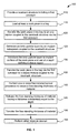
- FIG. 1 is a simplified diagram illustrating a method of processing a film of material in a tool having a race track configuration according to an embodiment of the present invention
- FIG. 2 is a simplified top-view diagram of a system and process in a race track configuration according to an embodiment of the present invention.
- FIG. 3 is a simplified top-view diagram of a system employing two race tracks in communication with one another.
- FIG. 4 is a simplified top-view diagram of a system employing a runway type architecture.
- FIG. 5 is a simplified top-view diagram of a system employing a rotating platen rather than conveyor belts, for movement of trays, bricks, or substrates.
- embodiments according to the present invention provide a method to form a free standing thickness of material from a semiconductor work piece.
- the free standing layer of material is provided using a plurality of high energy particles to cause a formation of a cleave plane in the semiconductor substrate.
- the method according to present invent invention can be used in a variety of application, including but not limited to semiconductor device packaging, photovoltaic cells, MEMS devices, and others.
- FIG. 1 is a simplified diagram illustrating a method of processing a film of material in a tool having a racetrack configuration according to an embodiment of the present invention.
- a method 100 for fabricating free standing thickness of materials from a semiconductor work piece in bulk form is provided as follows:
- Process 110 Provide a racetrack structure including a first conveyor;
- Process 115 Load at least a work piece in a tray
- Process 120 Transfer the work piece in the tray to an end station coupled to the racetrack structure via the first conveyor;
- Process 125 Generate an ionic particle beam by an implant subsystem coupled to the racetrack structure;
- Process 130 Introduce the ionic particle beam to implant surface of the work piece and rest at a depth defining a cleave region;
- Process 135 Transfer the work piece in the tray via the first conveyor to a cleave module coupled to the racetrack structure;
- Process 140 Perform one or more thermal-mechanical processes to cleave a free-standing thickness of material
- Process 145 Release the free standing thickness of material having a thickness substantially equal to the depth
- Process 150 Transfer the free standing thickness of material
- Process 155 Perform other steps as desired.
- the above sequence of steps provide a method of forming substrates using an implantation process and a cleave process according to an embodiment of the present invention.
- the method 100 includes using an accelerator based high energy implant process and a controlled cleave process to remove a film of material, which is preferably thick and free standing using a system configured in a race track manner.
- steps may be added, one or more steps may be removed, or one or more steps may be provided in a different sequence without departing from the scope of the claims herein. Further details of the present method can be found throughout the present specific and more particularly below.
- the method 100 includes at least two major processes.
- the first major process is implantation process including at least the Processes 120 and 125 , in which the surface of the work piece is exposed to an energetic particle beam.
- the work piece is an ingot or boule of crystalline silicon with a surface prepared to be substantially within a specific crystallographic plane, e.g., an (111) or (110) plane with a miscut angle in a few degrees.
- the energetic particle beam can be a beam of light ions such as hydrogen which are accelerated to high energy of greater than 1 MeV via a corresponding high current high energy accelerator.
- the beam of ions then is directed and tuned to have a desired spot size and controllable scanning scheme via a magnetic beam scanner.
- the implantation process is performed within an implant subsystem coupled to a racetrack structure which is scalable and modular for coupling with other process or service modules.
- a racetrack structure will be described in more detail in FIG. 2 below.
- a second major process of the method 100 is the actual cleaving of the work piece or processing to cause a facture propagation to form a free standing thickness of material.
- This process including at least Processes 140 through 150 , is usually performed within a cleave module coupled to the racetrack structure and separated from the end station for implantation process.
- this process includes one or more thermal-mechanical treatments of the work piece which has been pre-implanted by the high energy ion beam with a well-defined cleave region.
- at least a localized initiation region at a defined depth has been formed beneath the surface of the work piece by implanting a beam of ions to a portion of the surface.
- the one or more thermal-mechanical treatments can be performed, at least starting from the initiation region, to initiate a facture locally. Further, the thermal-mechanical process is to cause the facture to subsequently propagate along the cleave region or layer, which is preferably close to a pre-defined crystallographic plane (such as (111) plane) due to a smaller cost of energy. Finally, the process results in separating a thin upper layer of the work piece from the remainder of the work piece.
- the thin upper layer is a monolithic, free standing thickness of material with a thickness substantially equal to the depth of the cleave layer. Through one or more extra steps, the free standing thickness of material can be released and transferred out of the cleave module via an output port.
- the released free standing thickness of material can be called a wafer that self-supporting and can be used as a wafer substrates for many applications including solar cells. Details about techniques of controlled cleaving a free standing thickness of materials and associated examples of the cleaving process tools can be found in U.S. Pat. No. 6,013,563 and U.S. Patent Application No. 61/051,344, U.S. Patent Application No. 61/051,307, commonly assigned to Silicon Genesis Corporation of San Jose, Calif., and hereby incorporated by reference for all purposes. Of course, there can be other variations, alternatives, and modifications.
- the present method can perform other processes.
- the method can place the thickness of detached material on a support member, which is later processed.
- the method performs one or more processes on the semiconductor substrate before subjecting the surface region with the first plurality of high energy particles.
- the processes can be for the formation of photovoltaic cells, integrated circuits, optical devices, any combination of these, and the like.
- FIG. 2 is a simplified top-view diagram of a system and process in a racetrack configuration according to an embodiment of the present invention.
- a factory volume manufacture system is provided and configured in a racetrack structure 1000 .
- the racetrack structure 1000 is illustrated specifically as a closed loop architecture. Of course, other forms such as linear single runway or multiple parallel runways architectures can be applicable.
- the racetrack structure inherently includes a track route and a factory conveyor can be built along with.
- a sample tray 1100 then is able to be installed onto the track route and transferable via this conveyor from one location to another. For example, the arrows within the track route illustrate the directions of the tray 1100 being transferred.
- a tray service module 1200 can be coupled to the racetrack structure 1000 .
- the tray module 1200 can be used for stationing the sample tray 1100 , where one or more work pieces can be loaded.
- the sample tray 1100 is designed to be able to carry multiple work pieces for maximizing the manufacture throughput.
- the tray 1100 can have 6 ⁇ 6 pallets each seated a 156 ⁇ 156 mm ingots or can have 8 ⁇ 8 pallets each seated a 125 ⁇ 125 mm ingots. Each ingots can have a total height up to 100 mm.
- the throughput of each implant/cleave process pair is expected to range from 185 to 300 wafers per hour depending on wafer form factors. In an embodiment, more than one tray can be installed for increasing the production.
- the factory volume manufacture system includes one or more implant subsystems.
- Each of the implant subsystem includes an accelerator-based ion implanter (e.g. 1001 ) and an end station (e.g. 1011 ).
- the tray 1100 can be loaded into the end station 1011 , which is a vacuum chamber and coupled to the accelerator 1001 for performing an implantation process to at least one work piece in the tray 1100 .
- the accelerator-based ion implanter 1001 is characterized as a high current, high energy ion beam accelerator and designed to produce a mono-energetic beam of protons or other light ions at energy greater than 1 MeV.
- a RFQ-based or RFI-based linear accelerator is used.
- a cyclotron accelerator is applied.
- an electrostatic accelerator can be used. Ion implant apparatuses useful for embodiments of the present invention have been made recently available by the use of DC electrostatic particle accelerators such as the DYNAMITRON proton accelerator available from Ion Beam Applications SA, Belgium). Other forms of DC electrostatic accelerators which may be used include Van de Graaff or Tandem Van de Graaff accelerator types.
- the proton beam generated by the accelerator 1001 is directed into the end station 1011 and tuned with a proper spot diameter and dose control.
- the surfaces of the work pieces in the tray 1100 is exposed to the proton beam which can be scanned and pulsed to provide proper dosage across the surface area.
- the energetic ions then are implanted into the surface of each work piece and rest at a well-defined depth depending on the energy level of the beam, causing a formation of a stressed defective structure within a thin layer called a cleave region or cleave layer.
- another implant subsystem includes an accelerator 1002 (or 1003 , or 100 N) and an end station 1012 (or 1013 , or 101 N) accordingly for performing similar implantation process to a separate tray holding at least one work piece.
- the racetrack structure 1000 also is configured to couple with several process or service modules along the track route.
- one or more cleave module 1211 , 1212 , or 121 N are directly coupled to the racetrack structure 1000 .
- the tray 1100 can be transferred via the conveyor into the cleave module 121 1 .
- the cleave module 1211 includes tools for performing one or more thermal-mechanical treatments to the work pieces in the tray 1100 .
- the thermal-mechanical treatments are applied and controlled to cause an initiation of mechanical fracture of the work piece near the cleave region and a subsequent controlled propagation along the cleave region.
- the thermal-mechanical treatments cause a cleave process or a controlled facture propagation of a thin upper layer of a bulk work piece.
- the cleave process would lead to a formation and detachment of a complete free standing thickness of material or a free standing film or simply a thin wafer out of each work piece in the tray.
- the number of the cleave modules associated with the racetrack structure 1000 can be increased, e.g., by adding redundant cleave modules 1212 through 121 N, for achieving a balanced line production with a proper ratio over the number of installed implant subsystems within the same racetrack structure 1000 .
- the racetrack structure 1000 can be designed to couple with an annealing station 1201 where the work pieces in the tray 1100 can be thermally treated before loaded into the cleave module 1211 .
- the racetrack structure 1000 can include an optional module 1221 for performing any necessary steps after the formation of the free standing thickness of material.
- each cleave module e.g., 1211 or 1212
- the racetrack structure may also include a quality control (QC) module 1231 for performing quality inspection for a remaining portion of each work piece in the tray 1100 after removing a free standing thickness of material thereof.
- the QC module 1231 may also be able to performing necessary work piece re-preparation including surface smoothening process to make each work piece ready for a repeated implant/cleave process.
- the tray 1100 carrying the work pieces can be transferred again into one of end stations 1011 through 101 N for next round of implantation process.
- FIG. 1 described above The details of a method for manufacturing a film of material subsequently in a tool having a racetrack configuration can be seen in FIG. 1 described above.
- FIG. 3 shows a simplified schematic diagram of an embodiment utilizing a race track having more than one loop.
- a first loop 300 of the racetrack is utilized to receive and circulate trays bearing work pieces between implant stations and cleave stations. Following cleaving, wafers are output to a conveyor.
- a second loop 302 of the race track is used to refill trays with bricks, once successive implantation and cleaving steps have reduced the amount of material present in an existing brick.
- the second race track is also in communication with various stations, such as a load lock, a brick inspection node, a brick grinding node, and a brick stocking point.
- FIGS. 2 and 3 show a closed-loop architecture, this is not required. According to alternative embodiments, a single runway architecture may be employed.
- FIG. 4 shows one such alternative embodiment utilizing a runway configuration.
- a single, linear conveyor 400 transports work pieces 402 (which may be supported on trays), for exposure to implantation in the end-station of one or more linear accelerators.
- the conveyor also is in communication with various other nodes, for example cleave modules or service modules that may be used for analysis or processing of wafers/substrates or the bricks.
- a robot 404 may be employed to transport bricks from regions near the end of the conveyor to the beginning of the conveyor. This transport would allow for implantation of the bricks in order to cleave additional material.
- the robot may be a track robot (shown) or may be an Automated Guide Vehicle (AGV).
- AGV Automated Guide Vehicle
- Still another example of an alternative embodiment employs a rotating lazy susan-type structure to accomplish movement.
- a circular platform 500 is configured to rotate to allow bricks/trays present thereon, to be in communication with different implantation stations or analysis processing nodes.
- the circular platform is also in communication with input and output nodes allowing successive loading and unloading of trays/bricks/cleaved substrates.
- the particles of hydrogen can be replaced using co-implantation of helium and hydrogen ions to allow for formation of the cleave plane with a modified dose and/or cleaving properties according to alternative embodiments.
- the work piece can be one or more silicon boules and/or waters, and the like.
- the work piece can be configured with a slight miscut or be spatially angled with or without miscuts.
Abstract
A system for manufacturing free-standing films from work pieces. The system includes a racetrack structure being configured to transfer at least one work piece and one or more accelerator-based ion implanters coupled to the racetrack structure via an end station. Each of the accelerator-based ion implanters is configured to introduce particles having an energy of greater than 1 MeV to implant into a surface of the work piece loaded in the end station to form a cleave region in the work piece. The system includes one or more cleave modules coupled to the racetrack structure configured to perform a cleave process to release a free-standing film from the work piece along the cleave region. Additionally, the system includes an output port coupled to each cleave module to output the free standing film detached from the work piece and one or more service modules each connected to the racetrack structure.
Description
The instant nonprovisional patent application claims priority to U.S. Provisional Patent Application No. 61/091,710, filed Aug. 25, 2008 and incorporated by reference in its entirety herein for all purposes.
The present invention relates generally to technique including a method and a structure for forming substrates. More particularly, the present method and system provides a method and system using an accelerator process for the manufacture of thick free standing semiconductor films for a variety of applications including photovoltaic cells. But it will be recognized that the invention has a wider range of applicability; it can also be applied to other types of applications such as for three-dimensional packaging of integrated semiconductor devices, photonic or optoelectronic devices, piezoelectronic devices, flat panel displays, microelectromechanical systems (“MEMS”), nano-technology structures, sensors, actuators, integrated circuits, biological and biomedical devices, and the like.
From the beginning of time, human beings have relied upon the “sun” to derive almost all useful forms of energy. Such energy comes from petroleum, radiant, wood, and various forms of thermal energy. As merely an example, human being have relied heavily upon petroleum sources such as coal and gas for much of their needs. Unfortunately, such petroleum sources have become depleted and have lead to other problems. As a replacement, in part, solar energy has been proposed to reduce our reliance on petroleum sources. As merely an example, solar energy can be derived from “solar cells” commonly made of silicon.
The silicon solar cell generates electrical power when exposed to solar radiation from the sun. The radiation interacts with atoms of the silicon and forms electrons and holes that migrate to p-doped and n-doped regions in the silicon body and create voltage differentials and an electric current between the doped regions. Depending upon the application, solar cells have been integrated with concentrating elements to improve efficiency. As an example, solar radiation accumulates and focuses using concentrating elements that direct such radiation to one or more portions of active photovoltaic materials. Although effective, these solar cells still have many limitations.
As merely an example, solar cells rely upon starting materials such as silicon. Such silicon is often made using either polysilicon (i.e. polycrystalline silicon) and/or single crystal silicon materials. These materials are often difficult to manufacture. Polysilicon cells are often formed by manufacturing polysilicon plates. Although these plates may be formed effectively, they do not possess optimum properties for highly effective solar cells. Single crystal silicon has suitable properties for high grade solar cells. Such single crystal silicon is, however, expensive and is also difficult to use for solar applications in an efficient and cost effective manner. Additionally, both polysilicon and single-crystal silicon materials suffer from material losses during conventional manufacturing called “kerf loss”, where the sawing process eliminates as much as 40% and even up to 60% of the starting material from a cast or grown boule and singulate the material into a wafer form factor. This is a highly inefficient method of preparing thin polysilicon or single-crystal silicon plates for solar cell use.
Generally, thin-film solar cells are less expensive by using less silicon material but their amorphous or polycrystalline structure are less efficient than the more expensive bulk silicon cells made from single-crystal silicon substrates. These and other limitations can be found throughout the present specification and more particularly below.
From the above, it is seen that techniques for forming suitable substrate materials of high quality and low cost are highly desired.
According to the present invention, techniques including a method and a structure for forming substrates are provided. More particularly, the present method and system provides a method and system using an accelerator process and a cleave process for the manufacture of thick free standing semiconductor films for a variety of applications including photovoltaic cells. But it will be recognized that the invention has a wider range of applicability; it can also be applied to other types of applications such as for three-dimensional packaging of integrated semiconductor devices, photonic or optoelectronic devices, piezoelectronic devices, flat panel displays, microelectromechanical systems (“MEMS”), nano-technology structures, sensors, actuators, integrated circuits, biological and biomedical devices, and the like.
In a specific embodiment, the present invention provides a system for manufacturing free standing films from bulk work pieces. The system includes a racetrack structure being configured to transfer at least one work piece. The system further includes one or more accelerator-based ion implanters coupled to the racetrack structure via an end station. Each of the accelerator-based ion implanters is configured to introduce particles having an energy of greater than 1 MeV to implant into a surface of the work piece loaded in the end station to form a cleave region in the work piece. Additionally, the system includes one or more cleave modules coupled to the racetrack structure. Each of the cleave modules is configured to perform a cleave process to release a free standing film from the work piece along the cleave region. Furthermore, the system includes an output port coupled to the cleave module to output the free standing film that is detached from the work piece and one or more service modules each connected to the racetrack structure.
In another specific embodiment, the present invention provides a method for volume manufacturing free standing thickness of materials from bulk work pieces. The method includes providing a racetrack structure including a first conveyor. The method further includes loading at least a work piece in a tray. The work piece has a surface substantially in a predetermined crystallographic plane. Additionally, the method includes transferring the work piece in the tray to an end station coupled to the racetrack structure via the first conveyor. The method further includes generating an ionic particle beam by an implant subsystem coupled to the racetrack structure. The ionic particle beam is introduced to the surface of the work piece in the end station and implanted to a depth defining a cleave region. Furthermore, the method includes transferring the work piece in the tray via the first conveyor to a cleave module coupled to the racetrack structure. The work piece is treated by one or more thermal-mechanical processes to cleave a free standing thickness of material along the cleave region. Moreover, the method includes releasing the free standing thickness of material having a thickness substantially equal to the depth and transferring the free standing thickness of material out of the cleave module via a second conveyor. In one embodiment, the racetrack structure is a closed looped architecture for transferring the tray holding a remaining portion of the work piece and performing a repeated implant process in the implant subsystem and a next round of cleave process in the cleave module.
Numerous benefits are achieved over pre-existing techniques using embodiments of the present invention. In particular, embodiments of the present invention use a cost effective accelerator system and method for providing a high energy implant process for layer transfer techniques. Such accelerator system may include, but is not limited to, a Drift Tube linear accelerator technique, a Radio Frequency Quadrupole (commonly called RFQ), an electrostatic accelerator technique, or combinations of these, (for example, a RFQ combined with a Drift Tube Linac or a RFI (RF-Focused Interdigital) Linear Accelerator), cyclotron, and other suitable techniques. In a preferred embodiment, the accelerator provides an implantation process that forms a thickness of transferable material defined by a cleave plane in a donor substrate. The thickness of transferable material may be further processed to provide a high quality semiconductor material for application such as photovoltaic devices, 3D MEMS or integrated circuits, IC packaging, semiconductor devices, any combination of these, and others. In a preferred embodiment, the present method provides for single crystal silicon for highly efficient photovoltaic cells among others. In a preferred embodiment, the present method and structure use a low initial dose of energetic particles, which allows the process to be cost effective and efficient. Additionally, the present method and structure allow for fabrication of large area substrates. It will be found that this invention can be applied to make thin silicon material plates of the desired form factor (for example, 50 μm-200 μm thickness with an area size from 15 cm×15 cm to upwards of 1 m×1 m or more for polysilicon plates). In an alternative preferred embodiment, embodiments according to the present invention may provide for a seed layer that can further provide for layering of a hetero-structure epitaxial process. The hetero-structure epitaxial process can be used to form thin multi-junction photovoltaic cells, among others. Merely as an example, GaAs and GaInP layers may be deposited heteroepitaxially onto a germanium seed layer, which is a transferred layer formed using an implant process according to an embodiment of the present invention. In a specific embodiment, the present method can be applied successively to cleaving multiple slices from a single ingot, e.g., silicon boule. That is, the method can be repeated to successively cleave slices (similar to cutting slices of bread from a baked loaf) according to a specific embodiment. Of course, there can be other variations, modifications, and alternatives.
Depending upon the embodiment, one or more of these benefits may be achieved. These and other benefits may be described throughout the present specification and more particularly below.
According to embodiments of the present invention, techniques including a method for forming substrates are provided. More particularly, embodiments according to the present invention provide a method to form a free standing thickness of material from a semiconductor work piece. In a specific embodiment, the free standing layer of material is provided using a plurality of high energy particles to cause a formation of a cleave plane in the semiconductor substrate. The method according to present invent invention can be used in a variety of application, including but not limited to semiconductor device packaging, photovoltaic cells, MEMS devices, and others.
1. Process 110: Provide a racetrack structure including a first conveyor;
2. Process 115: Load at least a work piece in a tray;
3. Process 120: Transfer the work piece in the tray to an end station coupled to the racetrack structure via the first conveyor;
4. Process 125: Generate an ionic particle beam by an implant subsystem coupled to the racetrack structure;
5. Process 130: Introduce the ionic particle beam to implant surface of the work piece and rest at a depth defining a cleave region;
6. Process 135: Transfer the work piece in the tray via the first conveyor to a cleave module coupled to the racetrack structure;
7. Process 140: Perform one or more thermal-mechanical processes to cleave a free-standing thickness of material;
8. Process 145: Release the free standing thickness of material having a thickness substantially equal to the depth;
9. Process 150: Transfer the free standing thickness of material;
10. Process 155: Perform other steps as desired.
The above sequence of steps provide a method of forming substrates using an implantation process and a cleave process according to an embodiment of the present invention. As shown, the method 100 includes using an accelerator based high energy implant process and a controlled cleave process to remove a film of material, which is preferably thick and free standing using a system configured in a race track manner. Other alternatives can also be provided where steps may be added, one or more steps may be removed, or one or more steps may be provided in a different sequence without departing from the scope of the claims herein. Further details of the present method can be found throughout the present specific and more particularly below.
Briefly, the method 100 includes at least two major processes. The first major process is implantation process including at least the Processes 120 and 125, in which the surface of the work piece is exposed to an energetic particle beam. For example, the work piece is an ingot or boule of crystalline silicon with a surface prepared to be substantially within a specific crystallographic plane, e.g., an (111) or (110) plane with a miscut angle in a few degrees. The energetic particle beam can be a beam of light ions such as hydrogen which are accelerated to high energy of greater than 1 MeV via a corresponding high current high energy accelerator. The beam of ions then is directed and tuned to have a desired spot size and controllable scanning scheme via a magnetic beam scanner. As the beam of ions is introduced to the surface of the work piece, the ions come to rest in a thin layer at a well-defined depth below the surface of the work piece, defining a cleave region or cleave layer thereof. This cleave region or layer establishes a plane along which a mechanical facture will preferentially propagate. Details about techniques using accelerator based ion implantation and examples of the implant tools thereof can be found in U.S. patent application Ser. No. 11/936,582, U.S. Patent Application No. 60/997,684, and U.S. Patent Application No. 60/992,086, commonly assigned to Silicon Genesis Corporation of San Jose, Calif., and hereby incorporated by reference for all purposes. In one embodiment, the implantation process is performed within an implant subsystem coupled to a racetrack structure which is scalable and modular for coupling with other process or service modules. For example, a racetrack structure will be described in more detail in FIG. 2 below.
A second major process of the method 100 is the actual cleaving of the work piece or processing to cause a facture propagation to form a free standing thickness of material. This process, including at least Processes 140 through 150, is usually performed within a cleave module coupled to the racetrack structure and separated from the end station for implantation process. In particular, this process includes one or more thermal-mechanical treatments of the work piece which has been pre-implanted by the high energy ion beam with a well-defined cleave region. In one implementation, at least a localized initiation region at a defined depth has been formed beneath the surface of the work piece by implanting a beam of ions to a portion of the surface. The one or more thermal-mechanical treatments can be performed, at least starting from the initiation region, to initiate a facture locally. Further, the thermal-mechanical process is to cause the facture to subsequently propagate along the cleave region or layer, which is preferably close to a pre-defined crystallographic plane (such as (111) plane) due to a smaller cost of energy. Finally, the process results in separating a thin upper layer of the work piece from the remainder of the work piece. The thin upper layer is a monolithic, free standing thickness of material with a thickness substantially equal to the depth of the cleave layer. Through one or more extra steps, the free standing thickness of material can be released and transferred out of the cleave module via an output port. The released free standing thickness of material can be called a wafer that self-supporting and can be used as a wafer substrates for many applications including solar cells. Details about techniques of controlled cleaving a free standing thickness of materials and associated examples of the cleaving process tools can be found in U.S. Pat. No. 6,013,563 and U.S. Patent Application No. 61/051,344, U.S. Patent Application No. 61/051,307, commonly assigned to Silicon Genesis Corporation of San Jose, Calif., and hereby incorporated by reference for all purposes. Of course, there can be other variations, alternatives, and modifications.
In a specific embodiment, the present method can perform other processes. For example, the method can place the thickness of detached material on a support member, which is later processed. Additionally or optionally, the method performs one or more processes on the semiconductor substrate before subjecting the surface region with the first plurality of high energy particles. Depending upon the embodiment, the processes can be for the formation of photovoltaic cells, integrated circuits, optical devices, any combination of these, and the like. Of course, there can be other variations, modifications, and alternatives.
In one embodiment, a tray service module 1200 can be coupled to the racetrack structure 1000. The tray module 1200 can be used for stationing the sample tray 1100, where one or more work pieces can be loaded. In an implementation, the sample tray 1100 is designed to be able to carry multiple work pieces for maximizing the manufacture throughput. For example, the tray 1100 can have 6×6 pallets each seated a 156×156 mm ingots or can have 8×8 pallets each seated a 125×125 mm ingots. Each ingots can have a total height up to 100 mm. In one implementation, the throughput of each implant/cleave process pair is expected to range from 185 to 300 wafers per hour depending on wafer form factors. In an embodiment, more than one tray can be installed for increasing the production.
In another embodiment, the factory volume manufacture system includes one or more implant subsystems. Each of the implant subsystem includes an accelerator-based ion implanter (e.g. 1001) and an end station (e.g. 1011). The tray 1100 can be loaded into the end station 1011, which is a vacuum chamber and coupled to the accelerator 1001 for performing an implantation process to at least one work piece in the tray 1100.
The accelerator-based ion implanter 1001 is characterized as a high current, high energy ion beam accelerator and designed to produce a mono-energetic beam of protons or other light ions at energy greater than 1 MeV. In one example, a RFQ-based or RFI-based linear accelerator is used. In another example, a cyclotron accelerator is applied. In yet another example, an electrostatic accelerator can be used. Ion implant apparatuses useful for embodiments of the present invention have been made recently available by the use of DC electrostatic particle accelerators such as the DYNAMITRON proton accelerator available from Ion Beam Applications SA, Belgium). Other forms of DC electrostatic accelerators which may be used include Van de Graaff or Tandem Van de Graaff accelerator types.
The proton beam generated by the accelerator 1001 is directed into the end station 1011 and tuned with a proper spot diameter and dose control. Within the end station 1011, the surfaces of the work pieces in the tray 1100 is exposed to the proton beam which can be scanned and pulsed to provide proper dosage across the surface area. The energetic ions then are implanted into the surface of each work piece and rest at a well-defined depth depending on the energy level of the beam, causing a formation of a stressed defective structure within a thin layer called a cleave region or cleave layer. In one implementation, there can be some additional implant subsystems being coupled to the racetrack structure 1000. For example, another implant subsystem includes an accelerator 1002 (or 1003, or 100N) and an end station 1012 (or 1013, or 101N) accordingly for performing similar implantation process to a separate tray holding at least one work piece.
Referring to FIG. 2 again, the racetrack structure 1000 also is configured to couple with several process or service modules along the track route. For example, one or more cleave module 1211, 1212, or 121N are directly coupled to the racetrack structure 1000. After the implantation process is performed within one of implant subsystems (described in last paragraph), the tray 1100 can be transferred via the conveyor into the cleave module 121 1. The cleave module 1211 includes tools for performing one or more thermal-mechanical treatments to the work pieces in the tray 1100. In particular, the thermal-mechanical treatments are applied and controlled to cause an initiation of mechanical fracture of the work piece near the cleave region and a subsequent controlled propagation along the cleave region. In one embodiment, the thermal-mechanical treatments cause a cleave process or a controlled facture propagation of a thin upper layer of a bulk work piece. The cleave process would lead to a formation and detachment of a complete free standing thickness of material or a free standing film or simply a thin wafer out of each work piece in the tray. In another embodiment, the number of the cleave modules associated with the racetrack structure 1000 can be increased, e.g., by adding redundant cleave modules 1212 through 121N, for achieving a balanced line production with a proper ratio over the number of installed implant subsystems within the same racetrack structure 1000.
Of course, there can be other alternatives, variations, and modifications for the system in the racetrack configuration. For example, the racetrack structure 1000 can be designed to couple with an annealing station 1201 where the work pieces in the tray 1100 can be thermally treated before loaded into the cleave module 1211. In another example, the racetrack structure 1000 can include an optional module 1221 for performing any necessary steps after the formation of the free standing thickness of material. In certain embodiments, each cleave module, e.g., 1211 or 1212, may include an output port 1311 or 1312 for transferring the free standing thickness of material after its detachment. The free standing thickness of material can be firstly inspected, and then boxed, or directly placed on a second conveyor 1300 associated with the racetrack structure 1000. In a specific embodiment, the racetrack structure may also include a quality control (QC) module 1231 for performing quality inspection for a remaining portion of each work piece in the tray 1100 after removing a free standing thickness of material thereof. The QC module 1231 may also be able to performing necessary work piece re-preparation including surface smoothening process to make each work piece ready for a repeated implant/cleave process. In particular, the tray 1100 carrying the work pieces can be transferred again into one of end stations 1011 through 101N for next round of implantation process. The details of a method for manufacturing a film of material subsequently in a tool having a racetrack configuration can be seen in FIG. 1 described above.
Alternative embodiments fall within the scope of the present invention. For example, FIG. 3 shows a simplified schematic diagram of an embodiment utilizing a race track having more than one loop. A first loop 300 of the racetrack is utilized to receive and circulate trays bearing work pieces between implant stations and cleave stations. Following cleaving, wafers are output to a conveyor.
A second loop 302 of the race track is used to refill trays with bricks, once successive implantation and cleaving steps have reduced the amount of material present in an existing brick. The second race track is also in communication with various stations, such as a load lock, a brick inspection node, a brick grinding node, and a brick stocking point.
While the embodiments of FIGS. 2 and 3 show a closed-loop architecture, this is not required. According to alternative embodiments, a single runway architecture may be employed.
Following cleaving, a robot 404 may be employed to transport bricks from regions near the end of the conveyor to the beginning of the conveyor. This transport would allow for implantation of the bricks in order to cleave additional material. In certain embodiments, the robot may be a track robot (shown) or may be an Automated Guide Vehicle (AGV).
And while the previous embodiments show systems having one or more conveyor structures, this is not required by the present invention. Alternative embodiments could use structures other than conveyors for movement of the trays/bricks/substrates. One example of alternative ways of moving these elements could utilize track-based robots. Another example of alternative ways of moving these elements could utilize AGVs.
Still another example of an alternative embodiment employs a rotating lazy susan-type structure to accomplish movement. As shown in the embodiment of FIG. 5 , a circular platform 500 is configured to rotate to allow bricks/trays present thereon, to be in communication with different implantation stations or analysis processing nodes. The circular platform is also in communication with input and output nodes allowing successive loading and unloading of trays/bricks/cleaved substrates.
The following nonprovisional patent applications are incorporated by reference in their entireties herein for all purposes: U.S. Nonprovisional patent application Ser. No. 11/782,289, and U.S. Nonprovisional patent application Ser. No. 11/784,524.
While the above is a full description of the specific embodiments, various modifications, alternative constructions and equivalents may be used. Although the above has been described using a selected sequence of steps, any combination of any elements of steps described as well as others may be used. Additionally, certain steps may be combined and/or eliminated depending upon the embodiment. Furthermore, the particles of hydrogen can be replaced using co-implantation of helium and hydrogen ions to allow for formation of the cleave plane with a modified dose and/or cleaving properties according to alternative embodiments. In other embodiments, the work piece can be one or more silicon boules and/or waters, and the like. In other embodiments, the work piece can be configured with a slight miscut or be spatially angled with or without miscuts. Of course there can be other variations, modifications, and alternatives. Therefore, the above description and illustrations should not be taken as limiting the scope of the present invention which is defined by the appended claims.
Claims (23)
1. A system for manufacturing free-standing films from bulk work pieces,the system comprising:
a racetrack structure being configured to transfer at least one work piece;
one or more accelerator-based ion implanters coupled to the racetrack structure via an end station, each of the accelerator-based ion implanters being configured to introduce particles to implant into a surface of the work piece loaded in the end station to form a cleave region in the work piece;
one or more cleave modules coupled to the racetrack structure, each of the cleave modules being configured to perform a cleave process to release a free-standing film from the work piece along the cleave region, whereupon following release of the free-standing film from the work piece, the work piece is returned to the end station for introduction of more particles; and
one or more service modules each connected to the racetrack structure;
wherein the one or more service modules include a quality control station for inspecting and preparing the work piece to be used for repeated implantation and cleave processes.
2. The system of claim 1 further comprising an output port coupled to the cleave module to output the free standing film that is detached from the work piece.
3. The system of claim 1 wherein the one or more service modules include a tray service module for loading one or more work pieces to a supporting tray, and performing a maintenance to the tray.
4. The system of claim 1 wherein the one or more service modules include an anneal station for performing thermal treatment before or after a cleave process in the one or more cleave modules.
5. The system of claim 1 wherein the at least one of the accelerator-based ion implanters is configured to introduce particles having an energy of greater than 1 MeV.
6. The system of claim 1 wherein the racetrack structure can be configured to be a closed loop architecture or a single runway architecture.
7. The system of claim 1 wherein the racetrack structure includes a first conveyor to transfer the at least one work piece in a tray from one location to another location, said another location including an end station, one of the one or more cleave modules, or one of the one or more service modules.
8. The system of claim 7 wherein the racetrack structure is scalable to extend the first conveyor and add additional process modules coupled thereto.
9. The system of claim 1 wherein the work piece is returned to the end station utilizing a track robot, a robotic arm, an automated guide vehicle, or a rotating platform.
10. The system of claim 1 further comprising a line balance for the racetrack structure with an adjustable ratio of a number of the one or more accelerator based ion implanters and a number of the one or more cleave modules.
11. A system for manufacturing free-standing films from bulk work pieces, the system comprising:
a racetrack structure being configured to transfer at least one work piece;
one or more accelerator-based ion implanters coupled to the racetrack structure via an end station, each of the accelerator-based ion implanters being configured to introduce particles to implant into a surface of the work piece loaded in the end station to form a cleave region in the work piece; and
one or more cleave modules coupled to the racetrack structure, each of the cleave modules being configured to perform a cleave process to release a free-standing film from the work piece along the cleave region, whereupon following release of the free-standing film from the work piece, the work piece is returned to the end station for introduction of more particles;
wherein the one or more accelerator-based ion implanters comprises a RFQ-based linear accelerator, a QFI-based linear accelerator, a cyclotron accelerator, or an electrostatic accelerator for producing particles having energy up to about 5 MeV.
12. The system of claim 11 wherein the particles include hydrogen ions or other light ions with either positive charges or negative charges.
13. The system of claim 11 wherein the work piece can be a boule of crystalline silicon and the surface can be selected to be along crystallographic (111) or (110) plane with a small miscut angles of a few degrees and square or pseudo-square cross-sectional shape.
14. The system of claim 11 wherein the one or more cleave modules further comprise tools for irradiating and scanning using an electronic-magnetic process to the work piece and performing a cleaving process.
15. A method for volume manufacturing free standing thickness of materials from bulk work pieces, the method comprising:
providing a racetrack structure including a first conveyor;
loading at least a work piece in the conveyor, the work piece having a surface substantially in a predetermined crystallographic plane;
transferring the work piece to an end station coupled to the racetrack structure via the first conveyor;
generating an ionic particle beam by an implant subsystem coupled to the racetrack structure, the ionic particle beam being introduced to the surface of the work piece in the end station and implanted to a depth defining a cleave region;
transferring the work piece via the first conveyor to a cleave module coupled to the racetrack structure, the work piece being treated by one or more processes to cleave a free standing thickness of material along the cleave region;
releasing the free standing thickness of material having a thickness substantially equal to the depth;
returning the work piece to the end station;
transferring the free standing thickness of material out of the cleave module via a second conveyor; and
transferring the free standing thickness of material to a QC module and performing inspection of the work piece within the QC module, the QC module being coupled to the racetrack structure.
16. The method of claim 15 wherein the loading at least a work piece in a tray is performed in a tray service module coupled to the racetrack structure.
17. The method of claim 15 wherein the tray is a platen comprising a plurality of pallets each being configured to hold one work piece with an mechanism to adjust relative surface angle and relative height.
18. The method of claim 15 wherein the racetrack structure can be configured to be a closed loop architecture or a single runway architecture.
19. The method of claim 15 wherein generating an ionic particle beam by the implant subsystem comprises using an accelerator to produce the ionic particle beam having an energy of a few MeV, redirecting the ionic particle beam to the end station, and using a magnetic scanner to scan the ionic particle beam.
20. The method of claim 15 wherein the depth defining the cleave region depends on an combination of energy level and dosage of the ionic particle beam.
21. The method of claim 15 further comprising annealing the work piece within an annealing module coupled to the racetrack structure before it is transferred to the cleave module via the first conveyor.
22. The method of claim 15 wherein the work piece is loaded in the conveyor supported on a tray.
23. The method of claim 15 wherein the work piece is returned to the end station utilizing a conveyor, a track robot, a robotic arm, an automated guide vehicle, or a rotating platform.
Priority Applications (1)
| Application Number | Priority Date | Filing Date | Title |
|---|---|---|---|
| US12/462,210 US8330126B2 (en) | 2008-08-25 | 2009-07-29 | Race track configuration and method for wafering silicon solar substrates |
Applications Claiming Priority (2)
| Application Number | Priority Date | Filing Date | Title |
|---|---|---|---|
| US9171008P | 2008-08-25 | 2008-08-25 | |
| US12/462,210 US8330126B2 (en) | 2008-08-25 | 2009-07-29 | Race track configuration and method for wafering silicon solar substrates |
Publications (2)
| Publication Number | Publication Date |
|---|---|
| US20100044595A1 US20100044595A1 (en) | 2010-02-25 |
| US8330126B2 true US8330126B2 (en) | 2012-12-11 |
Family
ID=41343195
Family Applications (1)
| Application Number | Title | Priority Date | Filing Date |
|---|---|---|---|
| US12/462,210 Expired - Fee Related US8330126B2 (en) | 2008-08-25 | 2009-07-29 | Race track configuration and method for wafering silicon solar substrates |
Country Status (4)
| Country | Link |
|---|---|
| US (1) | US8330126B2 (en) |
| EP (1) | EP2159025A3 (en) |
| KR (1) | KR101163282B1 (en) |
| CN (1) | CN101661973A (en) |
Cited By (6)
| Publication number | Priority date | Publication date | Assignee | Title |
|---|---|---|---|---|
| US9704835B2 (en) | 2015-01-09 | 2017-07-11 | Silicon Genesis Corporation | Three dimensional integrated circuit |
| US10049915B2 (en) | 2015-01-09 | 2018-08-14 | Silicon Genesis Corporation | Three dimensional integrated circuit |
| US10573627B2 (en) | 2015-01-09 | 2020-02-25 | Silicon Genesis Corporation | Three dimensional integrated circuit |
| US10804252B2 (en) | 2015-01-09 | 2020-10-13 | Silicon Genesis Corporation | Three dimensional integrated circuit |
| US11410984B1 (en) | 2021-10-08 | 2022-08-09 | Silicon Genesis Corporation | Three dimensional integrated circuit with lateral connection layer |
| US11670532B1 (en) * | 2021-12-06 | 2023-06-06 | Applied Materials, Inc. | System and method for controlling electrostatic clamping of multiple platens on a spinning disk |
Families Citing this family (5)
| Publication number | Priority date | Publication date | Assignee | Title |
|---|---|---|---|---|
| KR101915753B1 (en) * | 2010-10-21 | 2018-11-07 | 삼성디스플레이 주식회사 | Ion implantation system and method for implanting ions using the same |
| CN103646990A (en) * | 2013-11-28 | 2014-03-19 | 青岛蓝图文化传播有限公司市南分公司 | Cleavage method |
| CN105314362A (en) * | 2014-07-31 | 2016-02-10 | 晶彩科技股份有限公司 | Automatic transportation mechanism and method |
| CN108461555A (en) * | 2018-02-05 | 2018-08-28 | 宇泰(江西)新能源有限公司 | A kind of monocrystalline Silicon photrouics with Surface Texture structure |
| WO2020131431A1 (en) * | 2018-12-17 | 2020-06-25 | Applied Materials, Inc. | A method of forming devices on a substrate |
Citations (261)
| Publication number | Priority date | Publication date | Assignee | Title |
|---|---|---|---|---|
| DE834363C (en) | 1951-02-27 | 1952-03-20 | Zentral Werkstatt Goettingen | Method and device for the production of thin mica films |
| US2614055A (en) | 1947-05-12 | 1952-10-14 | Samica Corp | Method of treating mica |
| US3117002A (en) | 1960-02-16 | 1964-01-07 | Ampco Metal Inc | Aluminum bronze alloy having improved wear resistance by the addition of cobalt, chromium, and manganese |
| US3225820A (en) | 1962-11-01 | 1965-12-28 | Gen Precision Inc | Device for controlling temperature by heat conduction |
| US3390033A (en) | 1964-08-13 | 1968-06-25 | Rca Corp | Method of separating frit sealed parts of an electron tube |
| US3392069A (en) | 1963-07-17 | 1968-07-09 | Siemens Ag | Method for producing pure polished surfaces on semiconductor bodies |
| FR1558881A (en) | 1967-05-29 | 1969-02-28 | ||
| US3551213A (en) | 1968-09-04 | 1970-12-29 | Bell Telephone Labor Inc | Geometrically selective ion bombardment by means of the photoelectric effect |
| US3770499A (en) | 1972-02-28 | 1973-11-06 | Motorola Inc | Liquid phase deposition of thin insulating and refractory film on a substrate |
| US3786359A (en) | 1969-03-28 | 1974-01-15 | Alpha Ind Inc | Ion accelerator and ion species selector |
| US3806380A (en) | 1971-03-05 | 1974-04-23 | Hitachi Ltd | Method for hardening treatment of aluminum or aluminum-base alloy |
| US3832219A (en) | 1971-04-07 | 1974-08-27 | Atomic Energy Authority Uk | Methods of treating steel surfaces to modify their structure |
| FR2235474A1 (en) | 1973-06-28 | 1975-01-24 | Ibm | |
| US3900636A (en) | 1971-01-21 | 1975-08-19 | Gillette Co | Method of treating cutting edges |
| US3901423A (en) | 1973-11-26 | 1975-08-26 | Purdue Research Foundation | Method for fracturing crystalline materials |
| FR2261802A1 (en) | 1974-02-21 | 1975-09-19 | Devienne Fernand | |
| US3915757A (en) | 1972-08-09 | 1975-10-28 | Niels N Engel | Ion plating method and product therefrom |
| US3946334A (en) | 1973-11-14 | 1976-03-23 | Nippon Electric Company, Limited | Injection semiconductor laser device |
| US3957107A (en) | 1975-02-27 | 1976-05-18 | The United States Of America As Represented By The Secretary Of The Air Force | Thermal switch |
| US3964957A (en) | 1973-12-19 | 1976-06-22 | Monsanto Company | Apparatus for processing semiconductor wafers |
| FR2298880A1 (en) | 1975-01-22 | 1976-08-20 | Commissariat Energie Atomique | IONIC IMPLANTATION METHOD AND DEVICE |
| US3993909A (en) | 1973-03-16 | 1976-11-23 | U.S. Philips Corporation | Substrate holder for etching thin films |
| US4006340A (en) | 1973-09-28 | 1977-02-01 | Compagnie Industrielle Des Telecommunications Cit-Alcatel | Device for the rapid depositing of oxides in thin layers which adhere well to plastic supports |
| US4039416A (en) | 1975-04-21 | 1977-08-02 | White Gerald W | Gasless ion plating |
| US4053335A (en) | 1976-04-02 | 1977-10-11 | International Business Machines Corporation | Method of gettering using backside polycrystalline silicon |
| US4074139A (en) | 1976-12-27 | 1978-02-14 | Rca Corporation | Apparatus and method for maskless ion implantation |
| FR2266304B1 (en) | 1974-04-01 | 1978-07-13 | Philips Nv | |
| US4107350A (en) | 1972-08-14 | 1978-08-15 | Berg Joseph E | Method for depositing film on a substrate |
| US4108751A (en) | 1977-06-06 | 1978-08-22 | King William J | Ion beam implantation-sputtering |
| US4116751A (en) | 1975-10-08 | 1978-09-26 | Solomon Zaromb | Methods and apparatus for producing unsupported monocrystalline films of silicon and of other materials |
| US4121334A (en) | 1974-12-17 | 1978-10-24 | P. R. Mallory & Co. Inc. | Application of field-assisted bonding to the mass production of silicon type pressure transducers |
| US4170662A (en) | 1974-11-05 | 1979-10-09 | Eastman Kodak Company | Plasma plating |
| US4216906A (en) | 1976-06-21 | 1980-08-12 | Flow Research, Inc. | Method of making high velocity liquid jet |
| US4237601A (en) | 1978-10-13 | 1980-12-09 | Exxon Research & Engineering Co. | Method of cleaving semiconductor diode laser wafers |
| US4244348A (en) | 1979-09-10 | 1981-01-13 | Atlantic Richfield Company | Process for cleaving crystalline materials |
| US4252837A (en) | 1976-03-23 | 1981-02-24 | Warner-Lambert Company | Blade shields |
| US4255208A (en) | 1979-05-25 | 1981-03-10 | Ramot University Authority For Applied Research And Industrial Development Ltd. | Method of producing monocrystalline semiconductor films utilizing an intermediate water dissolvable salt layer |
| US4274004A (en) | 1979-02-02 | 1981-06-16 | Hitachi, Ltd. | Ion implanter |
| US4342631A (en) | 1980-06-16 | 1982-08-03 | Illinois Tool Works Inc. | Gasless ion plating process and apparatus |
| US4346123A (en) | 1979-08-02 | 1982-08-24 | Balzers Aktiengesellschaft | Method of depositing hard wear-resistant coatings on substrates |
| US4361600A (en) | 1981-11-12 | 1982-11-30 | General Electric Company | Method of making integrated circuits |
| US4368083A (en) | 1980-02-01 | 1983-01-11 | Commissariat A L'energie Atomique | Process for doping semiconductors |
| US4375125A (en) | 1980-03-07 | 1983-03-01 | U.S. Philips Corporation | Method of passivating pn-junction in a semiconductor device |
| FR2519437A1 (en) | 1982-01-04 | 1983-07-08 | Commissariat Energie Atomique | DEVICE FOR LIMITING AND CONTROLLING THE TEMPERATURE OF A TARGET BASED ON A SUPPORT IN A VACUUM ENCLOSURE AND RECEIVING AN ENERGY BEAM AND ITS APPLICATION TO THERMAL MEASUREMENTS |
| US4412868A (en) | 1981-12-23 | 1983-11-01 | General Electric Company | Method of making integrated circuits utilizing ion implantation and selective epitaxial growth |
| FR2529383A1 (en) | 1982-06-24 | 1983-12-30 | Commissariat Energie Atomique | MECHANICAL SCANNING TARGET HOLDER USABLE IN PARTICULAR FOR THE IMPLANTATION OF IORIS |
| US4452644A (en) | 1980-02-01 | 1984-06-05 | Commissariat A L'energie Atomique | Process for doping semiconductors |
| FR2537768A1 (en) | 1982-12-08 | 1984-06-15 | Commissariat Energie Atomique | METHOD AND DEVICE FOR OBTAINING SPATIALLY MODULATED DENSITY PARTICLE BEAMS, APPLICATION TO ION ETCHING AND IMPLANTATION |
| FR2537777A1 (en) | 1982-12-10 | 1984-06-15 | Commissariat Energie Atomique | METHOD AND DEVICE FOR IMPLANTATION OF PARTICLES IN A SOLID |
| US4468309A (en) | 1983-04-22 | 1984-08-28 | White Engineering Corporation | Method for resisting galling |
| US4471003A (en) | 1980-11-25 | 1984-09-11 | Cann Gordon L | Magnetoplasmadynamic apparatus and process for the separation and deposition of materials |
| US4486247A (en) | 1982-06-21 | 1984-12-04 | Westinghouse Electric Corp. | Wear resistant steel articles with carbon, oxygen and nitrogen implanted in the surface thereof |
| US4490190A (en) | 1981-03-13 | 1984-12-25 | Societe Anonyme Dite: Vide Et Traitement | Process for thermochemical treatments of metals by ionic bombardment |
| US4495219A (en) | 1981-10-09 | 1985-01-22 | Fujitsu Limited | Process for producing dielectric layers for semiconductor devices |
| US4500563A (en) | 1982-12-15 | 1985-02-19 | Pacific Western Systems, Inc. | Independently variably controlled pulsed R.F. plasma chemical vapor processing |
| US4530149A (en) | 1982-06-24 | 1985-07-23 | Rca Corporation | Method for fabricating a self-aligned vertical IGFET |
| FR2560426A1 (en) | 1984-02-28 | 1985-08-30 | Commissariat Energie Atomique | DEVICE FOR PRODUCING IONS OF A SPECIFIED SPECIES, USING FOR SEPARATION FROM OTHER IONS, ENERGY SELECTION, APPLICATION TO ION IMPLANTATION |
| US4539050A (en) | 1982-12-15 | 1985-09-03 | Wacker-Chemitronic Gesellschaft Fur Elektronik-Grundstoffe M.B.H. | Process for the manufacture of semiconductor wafers with a rear side having a gettering action |
| FR2563377A1 (en) | 1984-04-19 | 1985-10-25 | Commissariat Energie Atomique | METHOD FOR MANUFACTURING AN INSULATED INSULATED LAYER IN A SEMICONDUCTOR SUBSTRATE, BY ION IMPLANTATION |
| US4567505A (en) | 1983-10-27 | 1986-01-28 | The Board Of Trustees Of The Leland Stanford Junior University | Heat sink and method of attaching heat sink to a semiconductor integrated circuit and the like |
| US4566403A (en) | 1985-01-30 | 1986-01-28 | Sovonics Solar Systems | Apparatus for microwave glow discharge deposition |
| US4568563A (en) | 1983-08-02 | 1986-02-04 | Standard Telephones And Cables | Optical fibre manufacture |
| FR2575601A1 (en) | 1984-12-27 | 1986-07-04 | Commissariat Energie Atomique | Method and device for determining electrical parameters of a semiconductor layer as a function of depth |
| US4645546A (en) | 1984-07-13 | 1987-02-24 | Kabushiki Kaisha Toshiba | Semiconductor substrate |
| US4684535A (en) | 1984-03-03 | 1987-08-04 | Standard Telephones & Cables | Surface treatment of plastics material |
| US4706377A (en) | 1986-01-30 | 1987-11-17 | United Technologies Corporation | Passivation of gallium arsenide by nitrogen implantation |
| US4717683A (en) | 1986-09-23 | 1988-01-05 | Motorola Inc. | CMOS process |
| US4727047A (en) | 1980-04-10 | 1988-02-23 | Massachusetts Institute Of Technology | Method of producing sheets of crystalline material |
| US4764394A (en) | 1987-01-20 | 1988-08-16 | Wisconsin Alumni Research Foundation | Method and apparatus for plasma source ion implantation |
| US4766086A (en) | 1986-03-07 | 1988-08-23 | Kabushiki Kaisha Toshiba | Method of gettering a semiconductor device and forming an isolation region therein |
| US4837172A (en) | 1986-07-18 | 1989-06-06 | Matsushita Electric Industrial Co., Ltd. | Method for removing impurities existing in semiconductor substrate |
| US4846928A (en) | 1987-08-04 | 1989-07-11 | Texas Instruments, Incorporated | Process and apparatus for detecting aberrations in production process operations |
| US4847792A (en) | 1987-05-04 | 1989-07-11 | Texas Instruments Incorporated | Process and apparatus for detecting aberrations in production process operations |
| GB2211991A (en) | 1987-10-30 | 1989-07-12 | Atomic Energy Authority Uk | Electrical isolation of regions within semiconductor bodies |
| US4853250A (en) | 1988-05-11 | 1989-08-01 | Universite De Sherbrooke | Process of depositing particulate material on a substrate |
| US4883561A (en) | 1988-03-29 | 1989-11-28 | Bell Communications Research, Inc. | Lift-off and subsequent bonding of epitaxial films |
| US4887005A (en) | 1987-09-15 | 1989-12-12 | Rough J Kirkwood H | Multiple electrode plasma reactor power distribution system |
| US4891329A (en) | 1988-11-29 | 1990-01-02 | University Of North Carolina | Method of forming a nonsilicon semiconductor on insulator structure |
| US4894709A (en) | 1988-03-09 | 1990-01-16 | Massachusetts Institute Of Technology | Forced-convection, liquid-cooled, microchannel heat sinks |
| US4906594A (en) | 1987-06-12 | 1990-03-06 | Agency Of Industrial Science And Technology | Surface smoothing method and method of forming SOI substrate using the surface smoothing method |
| US4931405A (en) | 1988-02-08 | 1990-06-05 | Kabushiki Kaisha Toshiba | Method for manufacturing a semiconductor device and suppressing the generation of bulk microdefects near the substrate surface layer |
| US4948458A (en) | 1989-08-14 | 1990-08-14 | Lam Research Corporation | Method and apparatus for producing magnetically-coupled planar plasma |
| US4952273A (en) | 1988-09-21 | 1990-08-28 | Microscience, Inc. | Plasma generation in electron cyclotron resonance |
| US4956693A (en) | 1986-03-20 | 1990-09-11 | Hitachi, Ltd. | Semiconductor device |
| US4960073A (en) | 1988-09-19 | 1990-10-02 | Anelva Corporation | Microwave plasma treatment apparatus |
| GB2231197A (en) | 1989-03-06 | 1990-11-07 | Nordiko Ltd | Plasma apparatus electrode assembly |
| US4982090A (en) | 1988-02-05 | 1991-01-01 | Gesellschaft Fur Strahlen- Und Umweltforschung Mbh (Gsf) | Method and apparatus for the quantitative, depth differential analysis of solid samples with the use of two ion beams |
| US4983251A (en) | 1985-06-20 | 1991-01-08 | U.S. Philips Corporation | Method of manufacturing semiconductor devices |
| US4996077A (en) | 1988-10-07 | 1991-02-26 | Texas Instruments Incorporated | Distributed ECR remote plasma processing and apparatus |
| US5015353A (en) | 1987-09-30 | 1991-05-14 | The United States Of America As Represented By The Secretary Of The Navy | Method for producing substoichiometric silicon nitride of preselected proportions |
| US5034343A (en) | 1990-03-08 | 1991-07-23 | Harris Corporation | Manufacturing ultra-thin wafer using a handle wafer |
| US5070040A (en) | 1990-03-09 | 1991-12-03 | University Of Colorado Foundation, Inc. | Method and apparatus for semiconductor circuit chip cooling |
| US5082793A (en) | 1965-09-28 | 1992-01-21 | Li Chou H | Method for making solid state device utilizing ion implantation techniques |
| US5102821A (en) | 1990-12-20 | 1992-04-07 | Texas Instruments Incorporated | SOI/semiconductor heterostructure fabrication by wafer bonding of polysilicon to titanium |
| US5110748A (en) | 1991-03-28 | 1992-05-05 | Honeywell Inc. | Method for fabricating high mobility thin film transistors as integrated drivers for active matrix display |
| US5133826A (en) | 1989-03-09 | 1992-07-28 | Applied Microwave Plasma Concepts, Inc. | Electron cyclotron resonance plasma source |
| US5141878A (en) | 1990-04-02 | 1992-08-25 | At&T Bell Laboratories | Silicon photodiode for monolithic integrated circuits and method for making same |
| US5162241A (en) | 1990-07-05 | 1992-11-10 | Kabushiki Kaisha Toshiba | Method of manufacturing a semiconductor device |
| FR2681472A1 (en) | 1991-09-18 | 1993-03-19 | Commissariat Energie Atomique | PROCESS FOR PRODUCING THIN FILMS OF SEMICONDUCTOR MATERIAL |
| US5196355A (en) | 1989-04-24 | 1993-03-23 | Ibis Technology Corporation | Simox materials through energy variation |
| US5198371A (en) | 1990-09-24 | 1993-03-30 | Biota Corp. | Method of making silicon material with enhanced surface mobility by hydrogen ion implantation |
| US5198071A (en) | 1991-11-25 | 1993-03-30 | Applied Materials, Inc. | Process for inhibiting slip and microcracking while forming epitaxial layer on semiconductor wafer |
| US5202095A (en) | 1988-12-27 | 1993-04-13 | Matsushita Electric Industrial Co., Ltd. | Microwave plasma processor |
| US5203960A (en) | 1989-03-09 | 1993-04-20 | Applied Microwave Plasma Concepts, Inc. | Method of operation of electron cyclotron resonance plasma source |
| US5206749A (en) | 1990-12-31 | 1993-04-27 | Kopin Corporation | Liquid crystal display having essentially single crystal transistors pixels and driving circuits |
| US5213451A (en) | 1991-01-10 | 1993-05-25 | Wacker-Chemitronic Gesellschaft Fur Elektronik-Grundstoffe Mbh | Apparatus and method of automatically separating stacked wafers |
| US5213986A (en) | 1992-04-10 | 1993-05-25 | North American Philips Corporation | Process for making thin film silicon-on-insulator wafers employing wafer bonding and wafer thinning |
| US5234535A (en) | 1992-12-10 | 1993-08-10 | International Business Machines Corporation | Method of producing a thin silicon-on-insulator layer |
| US5234529A (en) | 1991-10-10 | 1993-08-10 | Johnson Wayne L | Plasma generating apparatus employing capacitive shielding and process for using such apparatus |
| US5242861A (en) | 1991-06-06 | 1993-09-07 | Nec Corporation | Method for manufacturing semiconductor device having a multilayer wiring structure |
| US5250328A (en) | 1991-04-30 | 1993-10-05 | Schott Glaswerke | Process and apparatus for plasma CVD coating or plasma treating substrates |
| US5252178A (en) | 1992-06-24 | 1993-10-12 | Texas Instruments Incorporated | Multi-zone plasma processing method and apparatus |
| US5256562A (en) | 1990-12-31 | 1993-10-26 | Kopin Corporation | Method for manufacturing a semiconductor device using a circuit transfer film |
| US5258325A (en) | 1990-12-31 | 1993-11-02 | Kopin Corporation | Method for manufacturing a semiconductor device using a circuit transfer film |
| US5258320A (en) | 1990-12-31 | 1993-11-02 | Kopin Corporation | Single crystal silicon arrayed devices for display panels |
| US5269880A (en) | 1992-04-03 | 1993-12-14 | Northern Telecom Limited | Tapering sidewalls of via holes |
| US5273610A (en) | 1992-06-23 | 1993-12-28 | Association Institutions For Material Sciences, Inc. | Apparatus and method for determining power in plasma processing |
| US5277748A (en) | 1992-01-31 | 1994-01-11 | Canon Kabushiki Kaisha | Semiconductor device substrate and process for preparing the same |
| EP0296804B1 (en) | 1987-06-24 | 1994-03-30 | Advanced Semiconductor Materials America, Inc. | Process for epitaxial deposition of silicone |
| US5303574A (en) | 1991-02-12 | 1994-04-19 | Hughes Aircraft Company | Evaluation of the extent of wear of articles |
| US5304509A (en) | 1992-08-24 | 1994-04-19 | Midwest Research Institute | Back-side hydrogenation technique for defect passivation in silicon solar cells |
| US5308776A (en) | 1991-02-20 | 1994-05-03 | Fujitsu Limited | Method of manufacturing SOI semiconductor device |
| US5342472A (en) | 1991-08-12 | 1994-08-30 | Tokyo Electron Limited | Plasma processing apparatus |
| US5344524A (en) | 1993-06-30 | 1994-09-06 | Honeywell Inc. | SOI substrate fabrication |
| US5354381A (en) | 1993-05-07 | 1994-10-11 | Varian Associates, Inc. | Plasma immersion ion implantation (PI3) apparatus |
| US5362671A (en) | 1990-12-31 | 1994-11-08 | Kopin Corporation | Method of fabricating single crystal silicon arrayed devices for display panels |
| US5363603A (en) | 1992-06-22 | 1994-11-15 | Alliant Techsystems, Inc. | Abrasive fluid jet cutting compositon and method |
| US5368710A (en) | 1992-05-14 | 1994-11-29 | Lam Research Corporation | Method of treating an article with a plasma apparatus in which a uniform electric field is induced by a dielectric window |
| US5370765A (en) | 1989-03-09 | 1994-12-06 | Applied Microwave Plasma Concepts, Inc. | Electron cyclotron resonance plasma source and method of operation |
| US5376560A (en) | 1992-04-03 | 1994-12-27 | National Semiconductor Corporation | Method for forming isolated semiconductor structures |
| US5404079A (en) | 1992-08-13 | 1995-04-04 | Matsushita Electric Industrial Co., Ltd. | Plasma generating apparatus |
| US5403434A (en) | 1994-01-06 | 1995-04-04 | Texas Instruments Incorporated | Low-temperature in-situ dry cleaning process for semiconductor wafer |
| US5405480A (en) | 1992-11-04 | 1995-04-11 | Novellus Systems, Inc. | Induction plasma source |
| WO1995010718A1 (en) | 1993-10-13 | 1995-04-20 | Zexel Torsen Inc. | Differential with friction-enhancing wedge |
| US5409563A (en) | 1993-02-26 | 1995-04-25 | Micron Technology, Inc. | Method for etching high aspect ratio features |
| US5411592A (en) | 1994-06-06 | 1995-05-02 | Ovonic Battery Company, Inc. | Apparatus for deposition of thin-film, solid state batteries |
| US5413679A (en) | 1993-06-30 | 1995-05-09 | The United States Of America As Represented By The Secretary Of The Navy | Method of producing a silicon membrane using a silicon alloy etch stop layer |
| US5427052A (en) | 1991-04-27 | 1995-06-27 | Shin-Etsu Handotai Co., Ltd. | Method and apparatus for production of extremely thin SOI film substrate |
| FR2714524A1 (en) | 1993-12-23 | 1995-06-30 | Commissariat Energie Atomique | Method of producing a relief structure on a support made of semiconductor material |
| US5435880A (en) | 1992-10-14 | 1995-07-25 | Tokyo Ohka Kogyo Co., Ltd. | Plasma processing apparatus |
| FR2715502A1 (en) | 1994-01-26 | 1995-07-28 | Commissariat Energie Atomique | Structure having cavities and method for producing such a structure |
| FR2715501A1 (en) | 1994-01-26 | 1995-07-28 | Commissariat Energie Atomique | Process for depositing semiconductor blades on a support |
| US5443661A (en) | 1993-07-27 | 1995-08-22 | Nec Corporation | SOI (silicon on insulator) substrate with enhanced gettering effects |
| US5444557A (en) | 1990-12-31 | 1995-08-22 | Kopin Corporation | Single crystal silicon arrayed devices for projection displays |
| US5459016A (en) | 1993-12-16 | 1995-10-17 | Minnesota Mining And Manufacturing Company | Nanostructured thermal transfer donor element |
| WO1995031825A1 (en) | 1994-05-18 | 1995-11-23 | Commissariat A L'energie Atomique | Method for production of a structure with a low level of dislocations and having an oxide layer buried in a semiconductor substrate |
| US5475514A (en) | 1990-12-31 | 1995-12-12 | Kopin Corporation | Transferred single crystal arrayed devices including a light shield for projection displays |
| US5476691A (en) | 1994-01-21 | 1995-12-19 | International Business Machines, Inc. | Surface treatment of magnetic recording heads |
| US5480842A (en) | 1994-04-11 | 1996-01-02 | At&T Corp. | Method for fabricating thin, strong, and flexible die for smart cards |
| US5487785A (en) | 1993-03-26 | 1996-01-30 | Tokyo Electron Kabushiki Kaisha | Plasma treatment apparatus |
| FR2725074A1 (en) | 1994-09-22 | 1996-03-29 | Commissariat Energie Atomique | PROCESS FOR MANUFACTURING A STRUCTURE INCLUDING A THIN SEMICONDUCTOR LAYER ON A SUBSTRATE |
| US5504328A (en) | 1994-12-09 | 1996-04-02 | Sematech, Inc. | Endpoint detection utilizing ultraviolet mass spectrometry |
| FR2715503B1 (en) | 1994-01-26 | 1996-04-05 | Commissariat Energie Atomique | Substrate for integrated components comprising a thin layer and its production method. |
| US5506176A (en) | 1992-12-07 | 1996-04-09 | Sony Corporation | Method of making a semiconductor device having a process of hydrogen annealing |
| US5508207A (en) | 1992-06-29 | 1996-04-16 | Sumitomo Sitix Corporation | Method of annealing a semiconductor wafer in a hydrogen atmosphere to desorb surface contaminants |
| US5514235A (en) | 1993-06-29 | 1996-05-07 | Shin-Etsu Handotai Co., Ltd. | Method of making bonded wafers |
| US5518965A (en) | 1993-07-09 | 1996-05-21 | France Telecom | Process for producing a structure integrating a cleaved optical guide with an optical fibre support for a guide-fibre optical coupling |
| US5528397A (en) | 1991-12-03 | 1996-06-18 | Kopin Corporation | Single crystal silicon transistors for display panels |
| US5539245A (en) | 1991-11-18 | 1996-07-23 | Mitsubishi Materials Silicon Corporation | Semiconductor substrate having a gettering layer |
| US5558718A (en) | 1994-04-08 | 1996-09-24 | The Regents, University Of California | Pulsed source ion implantation apparatus and method |
| US5569620A (en) | 1992-09-03 | 1996-10-29 | Harris Corporation | Bonded wafer processing with metal silicidation |
| US5581385A (en) | 1990-12-31 | 1996-12-03 | Kopin Corporation | Single crystal silicon arrayed devices for projection displays |
| US5585304A (en) | 1991-06-13 | 1996-12-17 | Agency Industrial Science | Method of making semiconductor device with multiple transparent layers |
| US5611855A (en) | 1995-01-31 | 1997-03-18 | Seh America, Inc. | Method for manufacturing a calibration wafer having a microdefect-free layer of a precisely predetermined depth |
| US5643834A (en) | 1991-07-01 | 1997-07-01 | Sumitomo Electric Industries, Ltd. | Process for manufacturing a semiconductor substrate comprising laminated copper, silicon oxide and silicon nitride layers |
| US5653811A (en) | 1995-07-19 | 1997-08-05 | Chan; Chung | System for the plasma treatment of large area substrates |
| US5686980A (en) | 1995-04-03 | 1997-11-11 | Kabushiki Kaisha Toshiba | Light-shielding film, useable in an LCD, in which fine particles of a metal or semi-metal are dispersed in and throughout an inorganic insulating film |
| US5700333A (en) | 1995-03-27 | 1997-12-23 | Semiconductor Energy Laboratory Co., Ltd. | Thin-film photoelectric conversion device and a method of manufacturing the same |
| US5705421A (en) | 1994-11-24 | 1998-01-06 | Sony Corporation | A SOI substrate fabricating method |
| US5710057A (en) | 1996-07-12 | 1998-01-20 | Kenney; Donald M. | SOI fabrication method |
| US5714395A (en) | 1995-09-13 | 1998-02-03 | Commissariat A L'energie Atomique | Process for the manufacture of thin films of semiconductor material |
| US5744852A (en) | 1995-05-17 | 1998-04-28 | Harris Corporation | Bonded wafer |
| US5753560A (en) | 1996-10-31 | 1998-05-19 | Motorola, Inc. | Method for fabricating a semiconductor device using lateral gettering |
| US5755914A (en) | 1992-08-25 | 1998-05-26 | Canon Kabushiki Kaisha | Method for bonding semiconductor substrates |
| US5763319A (en) | 1995-08-14 | 1998-06-09 | Advanced Materials Engineering | Process for fabricating semiconductor devices with shallowly doped regions using dopant compounds containing elements of high solid solubility |
| US5783022A (en) | 1995-10-31 | 1998-07-21 | Samsung Electronics Co., Ltd. | Apparatus and methods for wafer debonding using a liquid jet |
| US5793913A (en) | 1996-07-10 | 1998-08-11 | Northern Telecom Limited | Method for the hybrid integration of discrete elements on a semiconductor substrate |
| US5811348A (en) | 1995-02-02 | 1998-09-22 | Sony Corporation | Method for separating a device-forming layer from a base body |
| DE19753494A1 (en) | 1997-03-31 | 1998-10-01 | Mitsubishi Electric Corp | Silicon wafer especially SOI wafer production |
| US5821158A (en) | 1995-08-28 | 1998-10-13 | Nec Corporation | Substrate surface treatment method capable of removing a spontaneous oxide film at a relatively low temperature |
| US5824595A (en) | 1995-10-17 | 1998-10-20 | Deutsche Itt Industries Gmbh | Method of separating electronic elements |
| US5827751A (en) | 1991-12-06 | 1998-10-27 | Picogiga Societe Anonyme | Method of making semiconductor components, in particular on GaAs of InP, with the substrate being recovered chemically |
| US5840590A (en) | 1993-12-01 | 1998-11-24 | Sandia Corporation | Impurity gettering in silicon using cavities formed by helium implantation and annealing |
| US5841931A (en) | 1996-11-26 | 1998-11-24 | Massachusetts Institute Of Technology | Methods of forming polycrystalline semiconductor waveguides for optoelectronic integrated circuits, and devices formed thereby |
| US5854123A (en) | 1995-10-06 | 1998-12-29 | Canon Kabushiki Kaisha | Method for producing semiconductor substrate |
| US5869387A (en) | 1992-01-30 | 1999-02-09 | Canon Kabushiki Kaisha | Process for producing semiconductor substrate by heating to flatten an unpolished surface |
| US5869405A (en) | 1996-01-03 | 1999-02-09 | Micron Technology, Inc. | In situ rapid thermal etch and rapid thermal oxidation |
| US5877070A (en) | 1997-05-31 | 1999-03-02 | Max-Planck Society | Method for the transfer of thin layers of monocrystalline material to a desirable substrate |
| US5882987A (en) | 1997-08-26 | 1999-03-16 | International Business Machines Corporation | Smart-cut process for the production of thin semiconductor material films |
| EP0905767A1 (en) | 1997-09-26 | 1999-03-31 | Shin-Etsu Handotai Company Limited | Method of fabricating an SOI wafer and SOI wafer fabricated thereby |
| US5897743A (en) | 1996-01-22 | 1999-04-27 | Komatsu Electronic Metals Co., Ltd. | Jig for peeling a bonded wafer |
| US5906951A (en) | 1997-04-30 | 1999-05-25 | International Business Machines Corporation | Strained Si/SiGe layers on insulator |
| US5909627A (en) | 1998-05-18 | 1999-06-01 | Philips Electronics North America Corporation | Process for production of thin layers of semiconductor material |
| JP2901031B2 (en) | 1992-01-30 | 1999-06-02 | キヤノン株式会社 | Semiconductor substrate and method of manufacturing the same |
| JP2910001B2 (en) | 1992-01-30 | 1999-06-23 | キヤノン株式会社 | Semiconductor substrate and method of manufacturing the same |
| US5920764A (en) | 1997-09-30 | 1999-07-06 | International Business Machines Corporation | Process for restoring rejected wafers in line for reuse as new |
| WO1999035674A1 (en) | 1997-12-30 | 1999-07-15 | Commissariat A L'energie Atomique | Method for transferring a thin film comprising a step of generating inclusions |
| US5942050A (en) | 1994-12-02 | 1999-08-24 | Pacific Solar Pty Ltd. | Method of manufacturing a multilayer solar cell |
| US5953622A (en) | 1996-11-23 | 1999-09-14 | Hyundai Electronics Industries Co., Ltd. | Method for fabricating semiconductor wafers |
| US5966620A (en) | 1996-11-15 | 1999-10-12 | Canon Kabshiki Kaisha | Process for producing semiconductor article |
| US5966625A (en) | 1995-03-20 | 1999-10-12 | Toshiba Ceramics Co., Ltd. | Method for making a slant-surface silicon wafer having a reconstructed atomic-level stepped surface structure |
| US5968279A (en) | 1997-06-13 | 1999-10-19 | Mattson Technology, Inc. | Method of cleaning wafer substrates |
| US5985742A (en) | 1997-05-12 | 1999-11-16 | Silicon Genesis Corporation | Controlled cleavage process and device for patterned films |
| US5993677A (en) | 1996-01-25 | 1999-11-30 | Commissariat A L'energie Atomique | Process for transferring a thin film from an initial substrate onto a final substrate |
| US6004868A (en) | 1996-01-17 | 1999-12-21 | Micron Technology, Inc. | Method for CMOS well drive in a non-inert ambient |
| US6008128A (en) | 1997-07-18 | 1999-12-28 | Shin-Etsu Handotai Co., Ltd. | Method for smoothing surface of silicon single crystal substrate |
| EP0971395A1 (en) | 1998-07-07 | 2000-01-12 | Shin-Etsu Handotai Company Limited | "A method of fabricating an SOI wafer and SOI wafer fabricated by the method" |
| US6020252A (en) | 1996-05-15 | 2000-02-01 | Commissariat A L'energie Atomique | Method of producing a thin layer of semiconductor material |
| US6027988A (en) | 1997-05-28 | 2000-02-22 | The Regents Of The University Of California | Method of separating films from bulk substrates by plasma immersion ion implantation |
| US6033974A (en) | 1997-05-12 | 2000-03-07 | Silicon Genesis Corporation | Method for controlled cleaving process |
| US6066915A (en) | 1997-03-28 | 2000-05-23 | Pixtech Sa | Spacer arrangement in a flat display screen |
| US6077383A (en) | 1996-08-12 | 2000-06-20 | Commissariat A L'energie | Device for separating wafers and process for using said device |
| US6083324A (en) | 1998-02-19 | 2000-07-04 | Silicon Genesis Corporation | Gettering technique for silicon-on-insulator wafers |
| US6103599A (en) | 1997-07-25 | 2000-08-15 | Silicon Genesis Corporation | Planarizing technique for multilayered substrates |
| US6107653A (en) | 1997-06-24 | 2000-08-22 | Massachusetts Institute Of Technology | Controlling threading dislocation densities in Ge on Si using graded GeSi layers and planarization |
| US6107213A (en) | 1996-02-01 | 2000-08-22 | Sony Corporation | Method for making thin film semiconductor |
| US6120597A (en) | 1998-02-17 | 2000-09-19 | The Trustees Of Columbia University In The City Of New York | Crystal ion-slicing of single-crystal films |
| US6143628A (en) | 1997-03-27 | 2000-11-07 | Canon Kabushiki Kaisha | Semiconductor substrate and method of manufacturing the same |
| US6150239A (en) | 1997-05-31 | 2000-11-21 | Max Planck Society | Method for the transfer of thin layers monocrystalline material onto a desirable substrate |
| US6171965B1 (en) | 1999-04-21 | 2001-01-09 | Silicon Genesis Corporation | Treatment method of cleaved film for the manufacture of substrates |
| US6171982B1 (en) | 1997-12-26 | 2001-01-09 | Canon Kabushiki Kaisha | Method and apparatus for heat-treating an SOI substrate and method of preparing an SOI substrate by using the same |
| US6184111B1 (en) | 1998-06-23 | 2001-02-06 | Silicon Genesis Corporation | Pre-semiconductor process implant and post-process film separation |
| US6190998B1 (en) | 1996-05-15 | 2001-02-20 | Commissariat A L'energie Atomique | Method for achieving a thin film of solid material and applications of this method |
| US6191007B1 (en) | 1997-04-28 | 2001-02-20 | Denso Corporation | Method for manufacturing a semiconductor substrate |
| US6204151B1 (en) | 1999-04-21 | 2001-03-20 | Silicon Genesis Corporation | Smoothing method for cleaved films made using thermal treatment |
| US6214701B1 (en) | 1997-12-26 | 2001-04-10 | Sony Corporation | Semiconductor substrate and thin film semiconductor device, method of manufacturing the same, and anodizing apparatus |
| US6251754B1 (en) | 1997-05-09 | 2001-06-26 | Denso Corporation | Semiconductor substrate manufacturing method |
| US6263941B1 (en) | 1999-08-10 | 2001-07-24 | Silicon Genesis Corporation | Nozzle for cleaving substrates |
| US6274464B2 (en) | 1998-02-06 | 2001-08-14 | Texas Instruments Incorporated | Epitaxial cleaning process using HCL and N-type dopant gas to reduce defect density and auto doping effects |
| US6287941B1 (en) | 1999-04-21 | 2001-09-11 | Silicon Genesis Corporation | Surface finishing of SOI substrates using an EPI process |
| US6294478B1 (en) | 1996-02-28 | 2001-09-25 | Canon Kabushiki Kaisha | Fabrication process for a semiconductor substrate |
| US20010039095A1 (en) | 2000-01-21 | 2001-11-08 | Michel Marty | Process for producing a bipolar transistor with self-aligned emitter and extrinsic base |
| US6335269B1 (en) | 1998-09-04 | 2002-01-01 | Canon Kabushiki Kaisha | Semiconductor substrate and method for producing the same |
| US6342436B1 (en) | 1998-01-04 | 2002-01-29 | Sony Corporation | Method of manufacturing semiconductor substrate and method of manufacturing solid-state image-pickup device |
| US6376806B2 (en) | 2000-05-09 | 2002-04-23 | Woo Sik Yoo | Flash anneal |
| US6452091B1 (en) | 1999-07-14 | 2002-09-17 | Canon Kabushiki Kaisha | Method of producing thin-film single-crystal device, solar cell module and method of producing the same |
| US6455397B1 (en) | 1999-11-16 | 2002-09-24 | Rona E. Belford | Method of producing strained microelectronic and/or optical integrated and discrete devices |
| US20020174828A1 (en) | 2001-03-30 | 2002-11-28 | Memc Electronic Materials, Inc. | Thermal annealing process for producing silicon wafers with improved surface characteristics |
| US6503773B2 (en) | 2000-01-20 | 2003-01-07 | Amberwave Systems Corporation | Low threading dislocation density relaxed mismatched epilayers without high temperature growth |
| US6514836B2 (en) | 2001-06-04 | 2003-02-04 | Rona Elizabeth Belford | Methods of producing strained microelectronic and/or optical integrated and discrete devices |
| US6534381B2 (en) | 1999-01-08 | 2003-03-18 | Silicon Genesis Corporation | Method for fabricating multi-layered substrates |
| US20030077885A1 (en) | 2000-05-30 | 2003-04-24 | Bernard Aspar | Embrittled substrate and method for making same |
| US6563152B2 (en) | 2000-12-29 | 2003-05-13 | Intel Corporation | Technique to obtain high mobility channels in MOS transistors by forming a strain layer on an underside of a channel |
| US20030096098A1 (en) | 2001-10-05 | 2003-05-22 | Ovshinsky Stanford R. | Semiconductor with coordinatively irregular structures |
| US20030140844A1 (en) | 2002-01-31 | 2003-07-31 | Maa Jer-Shen | Method to form thick relaxed SiGe Layer with trench structure |
| US6621131B2 (en) | 2001-11-01 | 2003-09-16 | Intel Corporation | Semiconductor transistor having a stressed channel |
| US20030186493A1 (en) | 2000-04-03 | 2003-10-02 | Atsushi Iwasaki | Method and device for making substrates |
| US6723661B2 (en) | 2001-03-02 | 2004-04-20 | Amberwave Systems Corporation | Relaxed silicon germanium platform for high speed CMOS electronics and high speed analog circuits |
| EP1085562A3 (en) | 1999-09-17 | 2004-06-09 | Applied Materials, Inc. | Apparatus and method for surface finishing a silicon film |
| US20040253794A1 (en) | 2001-05-18 | 2004-12-16 | Faris Sadeg M. | MEMS and method of manufacturing MEMS |
| US6858107B2 (en) | 2002-07-17 | 2005-02-22 | S.O.I. Tec Silicon On Insulator Technologies S.A. | Method of fabricating substrates, in particular for optics, electronics or optoelectronics |
| US20050118754A1 (en) | 2003-11-18 | 2005-06-02 | Silicon Genesis Corporation | Method for fabricating semiconductor devices using strained silicon bearing material |
| US6911376B2 (en) | 2003-10-01 | 2005-06-28 | Wafermasters | Selective heating using flash anneal |
| US20050189013A1 (en) | 2003-12-23 | 2005-09-01 | Oliver Hartley | Process for manufacturing photovoltaic cells |
| US20060014366A1 (en) | 2002-06-07 | 2006-01-19 | Amberwave Systems Corporation | Control of strain in device layers by prevention of relaxation |
| US20060030122A1 (en) | 1996-08-27 | 2006-02-09 | Seiko Epson Corporation | Exfoliating method, transferring method of thin film device, and thin film device, thin film integrated circuit device, and liquid crystal display device produced by the same |
| US20060038182A1 (en) | 2004-06-04 | 2006-02-23 | The Board Of Trustees Of The University | Stretchable semiconductor elements and stretchable electrical circuits |
| US7019339B2 (en) | 2001-04-17 | 2006-03-28 | California Institute Of Technology | Method of using a germanium layer transfer to Si for photovoltaic applications and heterostructure made thereby |
| JP4076503B2 (en) | 2002-02-26 | 2008-04-16 | エボニック デグサ ゲーエムベーハー | CERAMIC MEMBRANE BASED ON SUPPORT WITH POLYMER FIBERS, PROCESS FOR PRODUCTION AND USE |
| US20110121207A1 (en) * | 2008-02-05 | 2011-05-26 | Vaxis Technologies Llc | Ion Beam Processing Apparatus |
| US8088669B2 (en) * | 2007-05-10 | 2012-01-03 | Semiconductor Energy Laboratory Co., Ltd. | Method for manufacturing substrate of semiconductor device |
Family Cites Families (6)
| Publication number | Priority date | Publication date | Assignee | Title |
|---|---|---|---|---|
| US610513A (en) | 1898-09-06 | Harry lourta broad | ||
| US5130708A (en) | 1991-03-11 | 1992-07-14 | Will Boyden, Inc. | Boat sinking warning device |
| EP1039513A3 (en) | 1999-03-26 | 2008-11-26 | Canon Kabushiki Kaisha | Method of producing a SOI wafer |
| JP2006294737A (en) | 2005-04-07 | 2006-10-26 | Sumco Corp | Method of manufacturing soi substrate and method of reproducing peeled wafer during manufacture thereof |
| JP2009532918A (en) * | 2006-04-05 | 2009-09-10 | シリコン ジェネシス コーポレーション | Manufacturing method and structure of solar cell using layer transfer process |
| US8153513B2 (en) * | 2006-07-25 | 2012-04-10 | Silicon Genesis Corporation | Method and system for continuous large-area scanning implantation process |
-
2009
- 2009-07-29 US US12/462,210 patent/US8330126B2/en not_active Expired - Fee Related
- 2009-08-25 KR KR1020090078839A patent/KR101163282B1/en not_active IP Right Cessation
- 2009-08-25 CN CN200910167477A patent/CN101661973A/en active Pending
- 2009-08-25 EP EP20090252046 patent/EP2159025A3/en not_active Withdrawn
Patent Citations (295)
| Publication number | Priority date | Publication date | Assignee | Title |
|---|---|---|---|---|
| US2614055A (en) | 1947-05-12 | 1952-10-14 | Samica Corp | Method of treating mica |
| DE834363C (en) | 1951-02-27 | 1952-03-20 | Zentral Werkstatt Goettingen | Method and device for the production of thin mica films |
| US3117002A (en) | 1960-02-16 | 1964-01-07 | Ampco Metal Inc | Aluminum bronze alloy having improved wear resistance by the addition of cobalt, chromium, and manganese |
| US3225820A (en) | 1962-11-01 | 1965-12-28 | Gen Precision Inc | Device for controlling temperature by heat conduction |
| US3392069A (en) | 1963-07-17 | 1968-07-09 | Siemens Ag | Method for producing pure polished surfaces on semiconductor bodies |
| US3390033A (en) | 1964-08-13 | 1968-06-25 | Rca Corp | Method of separating frit sealed parts of an electron tube |
| US5082793A (en) | 1965-09-28 | 1992-01-21 | Li Chou H | Method for making solid state device utilizing ion implantation techniques |
| FR1558881A (en) | 1967-05-29 | 1969-02-28 | ||
| US3551213A (en) | 1968-09-04 | 1970-12-29 | Bell Telephone Labor Inc | Geometrically selective ion bombardment by means of the photoelectric effect |
| US3786359A (en) | 1969-03-28 | 1974-01-15 | Alpha Ind Inc | Ion accelerator and ion species selector |
| US3900636A (en) | 1971-01-21 | 1975-08-19 | Gillette Co | Method of treating cutting edges |
| US3806380A (en) | 1971-03-05 | 1974-04-23 | Hitachi Ltd | Method for hardening treatment of aluminum or aluminum-base alloy |
| US3832219A (en) | 1971-04-07 | 1974-08-27 | Atomic Energy Authority Uk | Methods of treating steel surfaces to modify their structure |
| US3770499A (en) | 1972-02-28 | 1973-11-06 | Motorola Inc | Liquid phase deposition of thin insulating and refractory film on a substrate |
| US3915757A (en) | 1972-08-09 | 1975-10-28 | Niels N Engel | Ion plating method and product therefrom |
| US4107350A (en) | 1972-08-14 | 1978-08-15 | Berg Joseph E | Method for depositing film on a substrate |
| US3993909A (en) | 1973-03-16 | 1976-11-23 | U.S. Philips Corporation | Substrate holder for etching thin films |
| FR2235474A1 (en) | 1973-06-28 | 1975-01-24 | Ibm | |
| US4006340A (en) | 1973-09-28 | 1977-02-01 | Compagnie Industrielle Des Telecommunications Cit-Alcatel | Device for the rapid depositing of oxides in thin layers which adhere well to plastic supports |
| US3946334A (en) | 1973-11-14 | 1976-03-23 | Nippon Electric Company, Limited | Injection semiconductor laser device |
| US3901423A (en) | 1973-11-26 | 1975-08-26 | Purdue Research Foundation | Method for fracturing crystalline materials |
| US3964957A (en) | 1973-12-19 | 1976-06-22 | Monsanto Company | Apparatus for processing semiconductor wafers |
| FR2261802A1 (en) | 1974-02-21 | 1975-09-19 | Devienne Fernand | |
| FR2266304B1 (en) | 1974-04-01 | 1978-07-13 | Philips Nv | |
| US4170662A (en) | 1974-11-05 | 1979-10-09 | Eastman Kodak Company | Plasma plating |
| US4121334A (en) | 1974-12-17 | 1978-10-24 | P. R. Mallory & Co. Inc. | Application of field-assisted bonding to the mass production of silicon type pressure transducers |
| FR2298880A1 (en) | 1975-01-22 | 1976-08-20 | Commissariat Energie Atomique | IONIC IMPLANTATION METHOD AND DEVICE |
| US3957107A (en) | 1975-02-27 | 1976-05-18 | The United States Of America As Represented By The Secretary Of The Air Force | Thermal switch |
| US4039416A (en) | 1975-04-21 | 1977-08-02 | White Gerald W | Gasless ion plating |
| US4116751A (en) | 1975-10-08 | 1978-09-26 | Solomon Zaromb | Methods and apparatus for producing unsupported monocrystalline films of silicon and of other materials |
| US4252837A (en) | 1976-03-23 | 1981-02-24 | Warner-Lambert Company | Blade shields |
| US4053335A (en) | 1976-04-02 | 1977-10-11 | International Business Machines Corporation | Method of gettering using backside polycrystalline silicon |
| US4216906A (en) | 1976-06-21 | 1980-08-12 | Flow Research, Inc. | Method of making high velocity liquid jet |
| US4074139A (en) | 1976-12-27 | 1978-02-14 | Rca Corporation | Apparatus and method for maskless ion implantation |
| US4108751A (en) | 1977-06-06 | 1978-08-22 | King William J | Ion beam implantation-sputtering |
| US4237601A (en) | 1978-10-13 | 1980-12-09 | Exxon Research & Engineering Co. | Method of cleaving semiconductor diode laser wafers |
| US4274004A (en) | 1979-02-02 | 1981-06-16 | Hitachi, Ltd. | Ion implanter |
| US4255208A (en) | 1979-05-25 | 1981-03-10 | Ramot University Authority For Applied Research And Industrial Development Ltd. | Method of producing monocrystalline semiconductor films utilizing an intermediate water dissolvable salt layer |
| US4346123A (en) | 1979-08-02 | 1982-08-24 | Balzers Aktiengesellschaft | Method of depositing hard wear-resistant coatings on substrates |
| US4244348A (en) | 1979-09-10 | 1981-01-13 | Atlantic Richfield Company | Process for cleaving crystalline materials |
| US4452644A (en) | 1980-02-01 | 1984-06-05 | Commissariat A L'energie Atomique | Process for doping semiconductors |
| US4368083A (en) | 1980-02-01 | 1983-01-11 | Commissariat A L'energie Atomique | Process for doping semiconductors |
| US4375125A (en) | 1980-03-07 | 1983-03-01 | U.S. Philips Corporation | Method of passivating pn-junction in a semiconductor device |
| US4727047A (en) | 1980-04-10 | 1988-02-23 | Massachusetts Institute Of Technology | Method of producing sheets of crystalline material |
| US4342631A (en) | 1980-06-16 | 1982-08-03 | Illinois Tool Works Inc. | Gasless ion plating process and apparatus |
| US4471003A (en) | 1980-11-25 | 1984-09-11 | Cann Gordon L | Magnetoplasmadynamic apparatus and process for the separation and deposition of materials |
| US4490190A (en) | 1981-03-13 | 1984-12-25 | Societe Anonyme Dite: Vide Et Traitement | Process for thermochemical treatments of metals by ionic bombardment |
| US4495219A (en) | 1981-10-09 | 1985-01-22 | Fujitsu Limited | Process for producing dielectric layers for semiconductor devices |
| US4361600A (en) | 1981-11-12 | 1982-11-30 | General Electric Company | Method of making integrated circuits |
| US4412868A (en) | 1981-12-23 | 1983-11-01 | General Electric Company | Method of making integrated circuits utilizing ion implantation and selective epitaxial growth |
| FR2519437A1 (en) | 1982-01-04 | 1983-07-08 | Commissariat Energie Atomique | DEVICE FOR LIMITING AND CONTROLLING THE TEMPERATURE OF A TARGET BASED ON A SUPPORT IN A VACUUM ENCLOSURE AND RECEIVING AN ENERGY BEAM AND ITS APPLICATION TO THERMAL MEASUREMENTS |
| US4486247A (en) | 1982-06-21 | 1984-12-04 | Westinghouse Electric Corp. | Wear resistant steel articles with carbon, oxygen and nitrogen implanted in the surface thereof |
| US4508056A (en) | 1982-06-24 | 1985-04-02 | Commissariat A L'energie Atomique | Target holder with mechanical scanning |
| US4530149A (en) | 1982-06-24 | 1985-07-23 | Rca Corporation | Method for fabricating a self-aligned vertical IGFET |
| FR2529383A1 (en) | 1982-06-24 | 1983-12-30 | Commissariat Energie Atomique | MECHANICAL SCANNING TARGET HOLDER USABLE IN PARTICULAR FOR THE IMPLANTATION OF IORIS |
| US4536657A (en) | 1982-12-08 | 1985-08-20 | Commissariat A L'energie Atomique | Process and apparatus for obtaining beams of particles with a spatially modulated density |
| FR2537768A1 (en) | 1982-12-08 | 1984-06-15 | Commissariat Energie Atomique | METHOD AND DEVICE FOR OBTAINING SPATIALLY MODULATED DENSITY PARTICLE BEAMS, APPLICATION TO ION ETCHING AND IMPLANTATION |
| FR2537777A1 (en) | 1982-12-10 | 1984-06-15 | Commissariat Energie Atomique | METHOD AND DEVICE FOR IMPLANTATION OF PARTICLES IN A SOLID |
| US4585945A (en) | 1982-12-10 | 1986-04-29 | Commissariat A L'energie Atomique | Process and apparatus for implanting particles in a solid |
| US4500563A (en) | 1982-12-15 | 1985-02-19 | Pacific Western Systems, Inc. | Independently variably controlled pulsed R.F. plasma chemical vapor processing |
| US4539050A (en) | 1982-12-15 | 1985-09-03 | Wacker-Chemitronic Gesellschaft Fur Elektronik-Grundstoffe M.B.H. | Process for the manufacture of semiconductor wafers with a rear side having a gettering action |
| US4468309A (en) | 1983-04-22 | 1984-08-28 | White Engineering Corporation | Method for resisting galling |
| US4568563A (en) | 1983-08-02 | 1986-02-04 | Standard Telephones And Cables | Optical fibre manufacture |
| US4567505A (en) | 1983-10-27 | 1986-01-28 | The Board Of Trustees Of The Leland Stanford Junior University | Heat sink and method of attaching heat sink to a semiconductor integrated circuit and the like |
| FR2560426A1 (en) | 1984-02-28 | 1985-08-30 | Commissariat Energie Atomique | DEVICE FOR PRODUCING IONS OF A SPECIFIED SPECIES, USING FOR SEPARATION FROM OTHER IONS, ENERGY SELECTION, APPLICATION TO ION IMPLANTATION |
| US4684535A (en) | 1984-03-03 | 1987-08-04 | Standard Telephones & Cables | Surface treatment of plastics material |
| US4704302A (en) | 1984-04-19 | 1987-11-03 | Commissariat A L'energie Atomique | Process for producing an insulating layer buried in a semiconductor substrate by ion implantation |
| FR2563377A1 (en) | 1984-04-19 | 1985-10-25 | Commissariat Energie Atomique | METHOD FOR MANUFACTURING AN INSULATED INSULATED LAYER IN A SEMICONDUCTOR SUBSTRATE, BY ION IMPLANTATION |
| US4645546A (en) | 1984-07-13 | 1987-02-24 | Kabushiki Kaisha Toshiba | Semiconductor substrate |
| FR2575601A1 (en) | 1984-12-27 | 1986-07-04 | Commissariat Energie Atomique | Method and device for determining electrical parameters of a semiconductor layer as a function of depth |
| US4566403A (en) | 1985-01-30 | 1986-01-28 | Sovonics Solar Systems | Apparatus for microwave glow discharge deposition |
| US4983251A (en) | 1985-06-20 | 1991-01-08 | U.S. Philips Corporation | Method of manufacturing semiconductor devices |
| US4706377A (en) | 1986-01-30 | 1987-11-17 | United Technologies Corporation | Passivation of gallium arsenide by nitrogen implantation |
| US4766086A (en) | 1986-03-07 | 1988-08-23 | Kabushiki Kaisha Toshiba | Method of gettering a semiconductor device and forming an isolation region therein |
| US4956693A (en) | 1986-03-20 | 1990-09-11 | Hitachi, Ltd. | Semiconductor device |
| US4837172A (en) | 1986-07-18 | 1989-06-06 | Matsushita Electric Industrial Co., Ltd. | Method for removing impurities existing in semiconductor substrate |
| US4717683A (en) | 1986-09-23 | 1988-01-05 | Motorola Inc. | CMOS process |
| US4764394A (en) | 1987-01-20 | 1988-08-16 | Wisconsin Alumni Research Foundation | Method and apparatus for plasma source ion implantation |
| US4847792A (en) | 1987-05-04 | 1989-07-11 | Texas Instruments Incorporated | Process and apparatus for detecting aberrations in production process operations |
| US4906594A (en) | 1987-06-12 | 1990-03-06 | Agency Of Industrial Science And Technology | Surface smoothing method and method of forming SOI substrate using the surface smoothing method |
| EP0296804B1 (en) | 1987-06-24 | 1994-03-30 | Advanced Semiconductor Materials America, Inc. | Process for epitaxial deposition of silicone |
| US4846928A (en) | 1987-08-04 | 1989-07-11 | Texas Instruments, Incorporated | Process and apparatus for detecting aberrations in production process operations |
| US4887005A (en) | 1987-09-15 | 1989-12-12 | Rough J Kirkwood H | Multiple electrode plasma reactor power distribution system |
| US5015353A (en) | 1987-09-30 | 1991-05-14 | The United States Of America As Represented By The Secretary Of The Navy | Method for producing substoichiometric silicon nitride of preselected proportions |
| GB2211991A (en) | 1987-10-30 | 1989-07-12 | Atomic Energy Authority Uk | Electrical isolation of regions within semiconductor bodies |
| US4982090A (en) | 1988-02-05 | 1991-01-01 | Gesellschaft Fur Strahlen- Und Umweltforschung Mbh (Gsf) | Method and apparatus for the quantitative, depth differential analysis of solid samples with the use of two ion beams |
| US4931405A (en) | 1988-02-08 | 1990-06-05 | Kabushiki Kaisha Toshiba | Method for manufacturing a semiconductor device and suppressing the generation of bulk microdefects near the substrate surface layer |
| US4894709A (en) | 1988-03-09 | 1990-01-16 | Massachusetts Institute Of Technology | Forced-convection, liquid-cooled, microchannel heat sinks |
| US4883561A (en) | 1988-03-29 | 1989-11-28 | Bell Communications Research, Inc. | Lift-off and subsequent bonding of epitaxial films |
| US4853250A (en) | 1988-05-11 | 1989-08-01 | Universite De Sherbrooke | Process of depositing particulate material on a substrate |
| US4960073A (en) | 1988-09-19 | 1990-10-02 | Anelva Corporation | Microwave plasma treatment apparatus |
| US4952273A (en) | 1988-09-21 | 1990-08-28 | Microscience, Inc. | Plasma generation in electron cyclotron resonance |
| US4996077A (en) | 1988-10-07 | 1991-02-26 | Texas Instruments Incorporated | Distributed ECR remote plasma processing and apparatus |
| US4891329A (en) | 1988-11-29 | 1990-01-02 | University Of North Carolina | Method of forming a nonsilicon semiconductor on insulator structure |
| US5202095A (en) | 1988-12-27 | 1993-04-13 | Matsushita Electric Industrial Co., Ltd. | Microwave plasma processor |
| GB2231197A (en) | 1989-03-06 | 1990-11-07 | Nordiko Ltd | Plasma apparatus electrode assembly |
| US5133826A (en) | 1989-03-09 | 1992-07-28 | Applied Microwave Plasma Concepts, Inc. | Electron cyclotron resonance plasma source |
| US5370765A (en) | 1989-03-09 | 1994-12-06 | Applied Microwave Plasma Concepts, Inc. | Electron cyclotron resonance plasma source and method of operation |
| US5203960A (en) | 1989-03-09 | 1993-04-20 | Applied Microwave Plasma Concepts, Inc. | Method of operation of electron cyclotron resonance plasma source |
| US5196355A (en) | 1989-04-24 | 1993-03-23 | Ibis Technology Corporation | Simox materials through energy variation |
| US4948458A (en) | 1989-08-14 | 1990-08-14 | Lam Research Corporation | Method and apparatus for producing magnetically-coupled planar plasma |
| US5034343A (en) | 1990-03-08 | 1991-07-23 | Harris Corporation | Manufacturing ultra-thin wafer using a handle wafer |
| US5070040A (en) | 1990-03-09 | 1991-12-03 | University Of Colorado Foundation, Inc. | Method and apparatus for semiconductor circuit chip cooling |
| US5141878A (en) | 1990-04-02 | 1992-08-25 | At&T Bell Laboratories | Silicon photodiode for monolithic integrated circuits and method for making same |
| US5162241A (en) | 1990-07-05 | 1992-11-10 | Kabushiki Kaisha Toshiba | Method of manufacturing a semiconductor device |
| US5198371A (en) | 1990-09-24 | 1993-03-30 | Biota Corp. | Method of making silicon material with enhanced surface mobility by hydrogen ion implantation |
| US5102821A (en) | 1990-12-20 | 1992-04-07 | Texas Instruments Incorporated | SOI/semiconductor heterostructure fabrication by wafer bonding of polysilicon to titanium |
| US5258325A (en) | 1990-12-31 | 1993-11-02 | Kopin Corporation | Method for manufacturing a semiconductor device using a circuit transfer film |
| US20010019371A1 (en) | 1990-12-31 | 2001-09-06 | Kopin Corporation | Method of transferring semiconductors |
| US5581385A (en) | 1990-12-31 | 1996-12-03 | Kopin Corporation | Single crystal silicon arrayed devices for projection displays |
| US5317236A (en) | 1990-12-31 | 1994-05-31 | Kopin Corporation | Single crystal silicon arrayed devices for display panels |
| US5258320A (en) | 1990-12-31 | 1993-11-02 | Kopin Corporation | Single crystal silicon arrayed devices for display panels |
| US5438241A (en) | 1990-12-31 | 1995-08-01 | Kopin Corporation | Single crystal silicon arrayed devices for display panels |
| US5362671A (en) | 1990-12-31 | 1994-11-08 | Kopin Corporation | Method of fabricating single crystal silicon arrayed devices for display panels |
| US5206749A (en) | 1990-12-31 | 1993-04-27 | Kopin Corporation | Liquid crystal display having essentially single crystal transistors pixels and driving circuits |
| US5377031A (en) | 1990-12-31 | 1994-12-27 | Kopin Corporation | Single crystal silicon tiles for liquid crystal display panels including light shielding layers |
| US5256562A (en) | 1990-12-31 | 1993-10-26 | Kopin Corporation | Method for manufacturing a semiconductor device using a circuit transfer film |
| US5444557A (en) | 1990-12-31 | 1995-08-22 | Kopin Corporation | Single crystal silicon arrayed devices for projection displays |
| US5475514A (en) | 1990-12-31 | 1995-12-12 | Kopin Corporation | Transferred single crystal arrayed devices including a light shield for projection displays |
| US5213451A (en) | 1991-01-10 | 1993-05-25 | Wacker-Chemitronic Gesellschaft Fur Elektronik-Grundstoffe Mbh | Apparatus and method of automatically separating stacked wafers |
| US5303574A (en) | 1991-02-12 | 1994-04-19 | Hughes Aircraft Company | Evaluation of the extent of wear of articles |
| US5308776A (en) | 1991-02-20 | 1994-05-03 | Fujitsu Limited | Method of manufacturing SOI semiconductor device |
| US5110748A (en) | 1991-03-28 | 1992-05-05 | Honeywell Inc. | Method for fabricating high mobility thin film transistors as integrated drivers for active matrix display |
| US5427052A (en) | 1991-04-27 | 1995-06-27 | Shin-Etsu Handotai Co., Ltd. | Method and apparatus for production of extremely thin SOI film substrate |
| US5250328A (en) | 1991-04-30 | 1993-10-05 | Schott Glaswerke | Process and apparatus for plasma CVD coating or plasma treating substrates |
| US5242861A (en) | 1991-06-06 | 1993-09-07 | Nec Corporation | Method for manufacturing semiconductor device having a multilayer wiring structure |
| US5585304A (en) | 1991-06-13 | 1996-12-17 | Agency Industrial Science | Method of making semiconductor device with multiple transparent layers |
| US5643834A (en) | 1991-07-01 | 1997-07-01 | Sumitomo Electric Industries, Ltd. | Process for manufacturing a semiconductor substrate comprising laminated copper, silicon oxide and silicon nitride layers |
| US5342472A (en) | 1991-08-12 | 1994-08-30 | Tokyo Electron Limited | Plasma processing apparatus |
| FR2681472A1 (en) | 1991-09-18 | 1993-03-19 | Commissariat Energie Atomique | PROCESS FOR PRODUCING THIN FILMS OF SEMICONDUCTOR MATERIAL |
| US5374564A (en) | 1991-09-18 | 1994-12-20 | Commissariat A L'energie Atomique | Process for the production of thin semiconductor material films |
| US5234529A (en) | 1991-10-10 | 1993-08-10 | Johnson Wayne L | Plasma generating apparatus employing capacitive shielding and process for using such apparatus |
| US5539245A (en) | 1991-11-18 | 1996-07-23 | Mitsubishi Materials Silicon Corporation | Semiconductor substrate having a gettering layer |
| US5198071A (en) | 1991-11-25 | 1993-03-30 | Applied Materials, Inc. | Process for inhibiting slip and microcracking while forming epitaxial layer on semiconductor wafer |
| US5528397A (en) | 1991-12-03 | 1996-06-18 | Kopin Corporation | Single crystal silicon transistors for display panels |
| US5827751A (en) | 1991-12-06 | 1998-10-27 | Picogiga Societe Anonyme | Method of making semiconductor components, in particular on GaAs of InP, with the substrate being recovered chemically |
| JP2910001B2 (en) | 1992-01-30 | 1999-06-23 | キヤノン株式会社 | Semiconductor substrate and method of manufacturing the same |
| EP0553852B1 (en) | 1992-01-30 | 2003-08-20 | Canon Kabushiki Kaisha | Process for producing semiconductor substrate |
| US5869387A (en) | 1992-01-30 | 1999-02-09 | Canon Kabushiki Kaisha | Process for producing semiconductor substrate by heating to flatten an unpolished surface |
| JP2901031B2 (en) | 1992-01-30 | 1999-06-02 | キヤノン株式会社 | Semiconductor substrate and method of manufacturing the same |
| US5277748A (en) | 1992-01-31 | 1994-01-11 | Canon Kabushiki Kaisha | Semiconductor device substrate and process for preparing the same |
| US5376560A (en) | 1992-04-03 | 1994-12-27 | National Semiconductor Corporation | Method for forming isolated semiconductor structures |
| US5269880A (en) | 1992-04-03 | 1993-12-14 | Northern Telecom Limited | Tapering sidewalls of via holes |
| US5213986A (en) | 1992-04-10 | 1993-05-25 | North American Philips Corporation | Process for making thin film silicon-on-insulator wafers employing wafer bonding and wafer thinning |
| US5368710A (en) | 1992-05-14 | 1994-11-29 | Lam Research Corporation | Method of treating an article with a plasma apparatus in which a uniform electric field is induced by a dielectric window |
| US5363603A (en) | 1992-06-22 | 1994-11-15 | Alliant Techsystems, Inc. | Abrasive fluid jet cutting compositon and method |
| US5273610A (en) | 1992-06-23 | 1993-12-28 | Association Institutions For Material Sciences, Inc. | Apparatus and method for determining power in plasma processing |
| US5252178A (en) | 1992-06-24 | 1993-10-12 | Texas Instruments Incorporated | Multi-zone plasma processing method and apparatus |
| US5508207A (en) | 1992-06-29 | 1996-04-16 | Sumitomo Sitix Corporation | Method of annealing a semiconductor wafer in a hydrogen atmosphere to desorb surface contaminants |
| US5404079A (en) | 1992-08-13 | 1995-04-04 | Matsushita Electric Industrial Co., Ltd. | Plasma generating apparatus |
| US5304509A (en) | 1992-08-24 | 1994-04-19 | Midwest Research Institute | Back-side hydrogenation technique for defect passivation in silicon solar cells |
| US5755914A (en) | 1992-08-25 | 1998-05-26 | Canon Kabushiki Kaisha | Method for bonding semiconductor substrates |
| US5569620A (en) | 1992-09-03 | 1996-10-29 | Harris Corporation | Bonded wafer processing with metal silicidation |
| US5435880A (en) | 1992-10-14 | 1995-07-25 | Tokyo Ohka Kogyo Co., Ltd. | Plasma processing apparatus |
| US5405480A (en) | 1992-11-04 | 1995-04-11 | Novellus Systems, Inc. | Induction plasma source |
| US5506176A (en) | 1992-12-07 | 1996-04-09 | Sony Corporation | Method of making a semiconductor device having a process of hydrogen annealing |
| US5234535A (en) | 1992-12-10 | 1993-08-10 | International Business Machines Corporation | Method of producing a thin silicon-on-insulator layer |
| US5409563A (en) | 1993-02-26 | 1995-04-25 | Micron Technology, Inc. | Method for etching high aspect ratio features |
| US5487785A (en) | 1993-03-26 | 1996-01-30 | Tokyo Electron Kabushiki Kaisha | Plasma treatment apparatus |
| US5354381A (en) | 1993-05-07 | 1994-10-11 | Varian Associates, Inc. | Plasma immersion ion implantation (PI3) apparatus |
| US5514235A (en) | 1993-06-29 | 1996-05-07 | Shin-Etsu Handotai Co., Ltd. | Method of making bonded wafers |
| US5413679A (en) | 1993-06-30 | 1995-05-09 | The United States Of America As Represented By The Secretary Of The Navy | Method of producing a silicon membrane using a silicon alloy etch stop layer |
| US5344524A (en) | 1993-06-30 | 1994-09-06 | Honeywell Inc. | SOI substrate fabrication |
| US5518965A (en) | 1993-07-09 | 1996-05-21 | France Telecom | Process for producing a structure integrating a cleaved optical guide with an optical fibre support for a guide-fibre optical coupling |
| US5443661A (en) | 1993-07-27 | 1995-08-22 | Nec Corporation | SOI (silicon on insulator) substrate with enhanced gettering effects |
| WO1995010718A1 (en) | 1993-10-13 | 1995-04-20 | Zexel Torsen Inc. | Differential with friction-enhancing wedge |
| US5840590A (en) | 1993-12-01 | 1998-11-24 | Sandia Corporation | Impurity gettering in silicon using cavities formed by helium implantation and annealing |
| US5459016A (en) | 1993-12-16 | 1995-10-17 | Minnesota Mining And Manufacturing Company | Nanostructured thermal transfer donor element |
| FR2714524A1 (en) | 1993-12-23 | 1995-06-30 | Commissariat Energie Atomique | Method of producing a relief structure on a support made of semiconductor material |
| US5494835A (en) | 1993-12-23 | 1996-02-27 | Commissariat A L'energie Atomique | Process for the production of a relief structure on a semiconductor material support |
| US5403434A (en) | 1994-01-06 | 1995-04-04 | Texas Instruments Incorporated | Low-temperature in-situ dry cleaning process for semiconductor wafer |
| US5476691A (en) | 1994-01-21 | 1995-12-19 | International Business Machines, Inc. | Surface treatment of magnetic recording heads |
| US5804086A (en) | 1994-01-26 | 1998-09-08 | Commissariat A L'energie Atomique | Structure having cavities and process for producing such a structure |
| FR2715503B1 (en) | 1994-01-26 | 1996-04-05 | Commissariat Energie Atomique | Substrate for integrated components comprising a thin layer and its production method. |
| US5559043A (en) | 1994-01-26 | 1996-09-24 | Commissariat A L'energie Atomique | Method for placing semiconductive plates on a support |
| FR2715502A1 (en) | 1994-01-26 | 1995-07-28 | Commissariat Energie Atomique | Structure having cavities and method for producing such a structure |
| FR2715501A1 (en) | 1994-01-26 | 1995-07-28 | Commissariat Energie Atomique | Process for depositing semiconductor blades on a support |
| EP0665588A1 (en) | 1994-01-26 | 1995-08-02 | Commissariat A L'energie Atomique | Deposition process of semiconductor layers on a support |
| WO1995020824A1 (en) | 1994-01-26 | 1995-08-03 | Commissariat A L'energie Atomique | Cavity-containing structure and method for making same |
| US5558718A (en) | 1994-04-08 | 1996-09-24 | The Regents, University Of California | Pulsed source ion implantation apparatus and method |
| US5480842A (en) | 1994-04-11 | 1996-01-02 | At&T Corp. | Method for fabricating thin, strong, and flexible die for smart cards |
| WO1995031825A1 (en) | 1994-05-18 | 1995-11-23 | Commissariat A L'energie Atomique | Method for production of a structure with a low level of dislocations and having an oxide layer buried in a semiconductor substrate |
| FR2720189A1 (en) | 1994-05-18 | 1995-11-24 | Commissariat Energie Atomique | Method for producing a structure with a low dislocation rate comprising an oxide layer buried in a semiconductor substrate. |
| US5411592A (en) | 1994-06-06 | 1995-05-02 | Ovonic Battery Company, Inc. | Apparatus for deposition of thin-film, solid state batteries |
| FR2725074A1 (en) | 1994-09-22 | 1996-03-29 | Commissariat Energie Atomique | PROCESS FOR MANUFACTURING A STRUCTURE INCLUDING A THIN SEMICONDUCTOR LAYER ON A SUBSTRATE |
| US5863830A (en) | 1994-09-22 | 1999-01-26 | Commissariat A L'energie Atomique | Process for the production of a structure having a thin semiconductor film on a substrate |
| US5705421A (en) | 1994-11-24 | 1998-01-06 | Sony Corporation | A SOI substrate fabricating method |
| US5942050A (en) | 1994-12-02 | 1999-08-24 | Pacific Solar Pty Ltd. | Method of manufacturing a multilayer solar cell |
| US5504328A (en) | 1994-12-09 | 1996-04-02 | Sematech, Inc. | Endpoint detection utilizing ultraviolet mass spectrometry |
| US5611855A (en) | 1995-01-31 | 1997-03-18 | Seh America, Inc. | Method for manufacturing a calibration wafer having a microdefect-free layer of a precisely predetermined depth |
| US5811348A (en) | 1995-02-02 | 1998-09-22 | Sony Corporation | Method for separating a device-forming layer from a base body |
| US5966625A (en) | 1995-03-20 | 1999-10-12 | Toshiba Ceramics Co., Ltd. | Method for making a slant-surface silicon wafer having a reconstructed atomic-level stepped surface structure |
| US5700333A (en) | 1995-03-27 | 1997-12-23 | Semiconductor Energy Laboratory Co., Ltd. | Thin-film photoelectric conversion device and a method of manufacturing the same |
| US5686980A (en) | 1995-04-03 | 1997-11-11 | Kabushiki Kaisha Toshiba | Light-shielding film, useable in an LCD, in which fine particles of a metal or semi-metal are dispersed in and throughout an inorganic insulating film |
| US5744852A (en) | 1995-05-17 | 1998-04-28 | Harris Corporation | Bonded wafer |
| US5653811A (en) | 1995-07-19 | 1997-08-05 | Chan; Chung | System for the plasma treatment of large area substrates |
| US5763319A (en) | 1995-08-14 | 1998-06-09 | Advanced Materials Engineering | Process for fabricating semiconductor devices with shallowly doped regions using dopant compounds containing elements of high solid solubility |
| US5821158A (en) | 1995-08-28 | 1998-10-13 | Nec Corporation | Substrate surface treatment method capable of removing a spontaneous oxide film at a relatively low temperature |
| US5714395A (en) | 1995-09-13 | 1998-02-03 | Commissariat A L'energie Atomique | Process for the manufacture of thin films of semiconductor material |
| US5854123A (en) | 1995-10-06 | 1998-12-29 | Canon Kabushiki Kaisha | Method for producing semiconductor substrate |
| US5824595A (en) | 1995-10-17 | 1998-10-20 | Deutsche Itt Industries Gmbh | Method of separating electronic elements |
| US5783022A (en) | 1995-10-31 | 1998-07-21 | Samsung Electronics Co., Ltd. | Apparatus and methods for wafer debonding using a liquid jet |
| US5869405A (en) | 1996-01-03 | 1999-02-09 | Micron Technology, Inc. | In situ rapid thermal etch and rapid thermal oxidation |
| US6194327B1 (en) | 1996-01-03 | 2001-02-27 | Micron Technology, Inc. | Rapid thermal etch and rapid thermal oxidation |
| US6004868A (en) | 1996-01-17 | 1999-12-21 | Micron Technology, Inc. | Method for CMOS well drive in a non-inert ambient |
| US5897743A (en) | 1996-01-22 | 1999-04-27 | Komatsu Electronic Metals Co., Ltd. | Jig for peeling a bonded wafer |
| US5993677A (en) | 1996-01-25 | 1999-11-30 | Commissariat A L'energie Atomique | Process for transferring a thin film from an initial substrate onto a final substrate |
| US6107213A (en) | 1996-02-01 | 2000-08-22 | Sony Corporation | Method for making thin film semiconductor |
| US6294478B1 (en) | 1996-02-28 | 2001-09-25 | Canon Kabushiki Kaisha | Fabrication process for a semiconductor substrate |
| EP0807970B1 (en) | 1996-05-15 | 2008-04-02 | Commissariat A L'energie Atomique | Method of manufacturing a thin semiconductor layer |
| US6225192B1 (en) | 1996-05-15 | 2001-05-01 | Commissariat A L'energie Atomique | Method of producing a thin layer of semiconductor material |
| US6809009B2 (en) | 1996-05-15 | 2004-10-26 | Commissariat A L'energie Atomique | Method of producing a thin layer of semiconductor material |
| US6190998B1 (en) | 1996-05-15 | 2001-02-20 | Commissariat A L'energie Atomique | Method for achieving a thin film of solid material and applications of this method |
| US6020252A (en) | 1996-05-15 | 2000-02-01 | Commissariat A L'energie Atomique | Method of producing a thin layer of semiconductor material |
| US5793913A (en) | 1996-07-10 | 1998-08-11 | Northern Telecom Limited | Method for the hybrid integration of discrete elements on a semiconductor substrate |
| US5710057A (en) | 1996-07-12 | 1998-01-20 | Kenney; Donald M. | SOI fabrication method |
| US6077383A (en) | 1996-08-12 | 2000-06-20 | Commissariat A L'energie | Device for separating wafers and process for using said device |
| US20060030122A1 (en) | 1996-08-27 | 2006-02-09 | Seiko Epson Corporation | Exfoliating method, transferring method of thin film device, and thin film device, thin film integrated circuit device, and liquid crystal display device produced by the same |
| US5753560A (en) | 1996-10-31 | 1998-05-19 | Motorola, Inc. | Method for fabricating a semiconductor device using lateral gettering |
| US5966620A (en) | 1996-11-15 | 1999-10-12 | Canon Kabshiki Kaisha | Process for producing semiconductor article |
| EP0843344B1 (en) | 1996-11-15 | 2002-01-23 | Canon Kabushiki Kaisha | Process for transferring a semiconductor layer using silicon on insulator (SOI) technology |
| US5953622A (en) | 1996-11-23 | 1999-09-14 | Hyundai Electronics Industries Co., Ltd. | Method for fabricating semiconductor wafers |
| US5841931A (en) | 1996-11-26 | 1998-11-24 | Massachusetts Institute Of Technology | Methods of forming polycrystalline semiconductor waveguides for optoelectronic integrated circuits, and devices formed thereby |
| US6143628A (en) | 1997-03-27 | 2000-11-07 | Canon Kabushiki Kaisha | Semiconductor substrate and method of manufacturing the same |
| US6066915A (en) | 1997-03-28 | 2000-05-23 | Pixtech Sa | Spacer arrangement in a flat display screen |
| DE19753494A1 (en) | 1997-03-31 | 1998-10-01 | Mitsubishi Electric Corp | Silicon wafer especially SOI wafer production |
| US6191007B1 (en) | 1997-04-28 | 2001-02-20 | Denso Corporation | Method for manufacturing a semiconductor substrate |
| US5906951A (en) | 1997-04-30 | 1999-05-25 | International Business Machines Corporation | Strained Si/SiGe layers on insulator |
| US6251754B1 (en) | 1997-05-09 | 2001-06-26 | Denso Corporation | Semiconductor substrate manufacturing method |
| US6162705A (en) | 1997-05-12 | 2000-12-19 | Silicon Genesis Corporation | Controlled cleavage process and resulting device using beta annealing |
| US6033974A (en) | 1997-05-12 | 2000-03-07 | Silicon Genesis Corporation | Method for controlled cleaving process |
| US6010579A (en) * | 1997-05-12 | 2000-01-04 | Silicon Genesis Corporation | Reusable substrate for thin film separation |
| US5985742A (en) | 1997-05-12 | 1999-11-16 | Silicon Genesis Corporation | Controlled cleavage process and device for patterned films |
| US6048411A (en) | 1997-05-12 | 2000-04-11 | Silicon Genesis Corporation | Silicon-on-silicon hybrid wafer assembly |
| US6013563A (en) | 1997-05-12 | 2000-01-11 | Silicon Genesis Corporation | Controlled cleaning process |
| US6159824A (en) | 1997-05-12 | 2000-12-12 | Silicon Genesis Corporation | Silicon-on-silicon wafer bonding process using a thin film blister-separation method |
| US6013567A (en) | 1997-05-12 | 2000-01-11 | Silicon Genesis Corporation | Controlled cleavage process using pressurized fluid |
| US5994207A (en) | 1997-05-12 | 1999-11-30 | Silicon Genesis Corporation | Controlled cleavage process using pressurized fluid |
| US6027988A (en) | 1997-05-28 | 2000-02-22 | The Regents Of The University Of California | Method of separating films from bulk substrates by plasma immersion ion implantation |
| US6150239A (en) | 1997-05-31 | 2000-11-21 | Max Planck Society | Method for the transfer of thin layers monocrystalline material onto a desirable substrate |
| US5877070A (en) | 1997-05-31 | 1999-03-02 | Max-Planck Society | Method for the transfer of thin layers of monocrystalline material to a desirable substrate |
| US5968279A (en) | 1997-06-13 | 1999-10-19 | Mattson Technology, Inc. | Method of cleaning wafer substrates |
| US6107653A (en) | 1997-06-24 | 2000-08-22 | Massachusetts Institute Of Technology | Controlling threading dislocation densities in Ge on Si using graded GeSi layers and planarization |
| US6291321B1 (en) | 1997-06-24 | 2001-09-18 | Massachusetts Institute Of Technology | Controlling threading dislocation densities in Ge on Si using graded GeSi layers and planarization |
| US6008128A (en) | 1997-07-18 | 1999-12-28 | Shin-Etsu Handotai Co., Ltd. | Method for smoothing surface of silicon single crystal substrate |
| US6103599A (en) | 1997-07-25 | 2000-08-15 | Silicon Genesis Corporation | Planarizing technique for multilayered substrates |
| US5882987A (en) | 1997-08-26 | 1999-03-16 | International Business Machines Corporation | Smart-cut process for the production of thin semiconductor material films |
| EP0905767A1 (en) | 1997-09-26 | 1999-03-31 | Shin-Etsu Handotai Company Limited | Method of fabricating an SOI wafer and SOI wafer fabricated thereby |
| US5920764A (en) | 1997-09-30 | 1999-07-06 | International Business Machines Corporation | Process for restoring rejected wafers in line for reuse as new |
| US6171982B1 (en) | 1997-12-26 | 2001-01-09 | Canon Kabushiki Kaisha | Method and apparatus for heat-treating an SOI substrate and method of preparing an SOI substrate by using the same |
| US6214701B1 (en) | 1997-12-26 | 2001-04-10 | Sony Corporation | Semiconductor substrate and thin film semiconductor device, method of manufacturing the same, and anodizing apparatus |
| WO1999035674A1 (en) | 1997-12-30 | 1999-07-15 | Commissariat A L'energie Atomique | Method for transferring a thin film comprising a step of generating inclusions |
| US6342436B1 (en) | 1998-01-04 | 2002-01-29 | Sony Corporation | Method of manufacturing semiconductor substrate and method of manufacturing solid-state image-pickup device |
| US6274464B2 (en) | 1998-02-06 | 2001-08-14 | Texas Instruments Incorporated | Epitaxial cleaning process using HCL and N-type dopant gas to reduce defect density and auto doping effects |
| US6120597A (en) | 1998-02-17 | 2000-09-19 | The Trustees Of Columbia University In The City Of New York | Crystal ion-slicing of single-crystal films |
| US6083324A (en) | 1998-02-19 | 2000-07-04 | Silicon Genesis Corporation | Gettering technique for silicon-on-insulator wafers |
| US5909627A (en) | 1998-05-18 | 1999-06-01 | Philips Electronics North America Corporation | Process for production of thin layers of semiconductor material |
| US6184111B1 (en) | 1998-06-23 | 2001-02-06 | Silicon Genesis Corporation | Pre-semiconductor process implant and post-process film separation |
| EP0971395A1 (en) | 1998-07-07 | 2000-01-12 | Shin-Etsu Handotai Company Limited | "A method of fabricating an SOI wafer and SOI wafer fabricated by the method" |
| US6335269B1 (en) | 1998-09-04 | 2002-01-01 | Canon Kabushiki Kaisha | Semiconductor substrate and method for producing the same |
| US6534381B2 (en) | 1999-01-08 | 2003-03-18 | Silicon Genesis Corporation | Method for fabricating multi-layered substrates |
| US6171965B1 (en) | 1999-04-21 | 2001-01-09 | Silicon Genesis Corporation | Treatment method of cleaved film for the manufacture of substrates |
| US6287941B1 (en) | 1999-04-21 | 2001-09-11 | Silicon Genesis Corporation | Surface finishing of SOI substrates using an EPI process |
| US6455399B2 (en) | 1999-04-21 | 2002-09-24 | Silicon Genesis Corporation | Smoothing method for cleaved films made using thermal treatment |
| US6969668B1 (en) | 1999-04-21 | 2005-11-29 | Silicon Genesis Corporation | Treatment method of film quality for the manufacture of substrates |
| US6204151B1 (en) | 1999-04-21 | 2001-03-20 | Silicon Genesis Corporation | Smoothing method for cleaved films made using thermal treatment |
| US6452091B1 (en) | 1999-07-14 | 2002-09-17 | Canon Kabushiki Kaisha | Method of producing thin-film single-crystal device, solar cell module and method of producing the same |
| US6513564B2 (en) | 1999-08-10 | 2003-02-04 | Silicon Genesis Corporation | Nozzle for cleaving substrates |
| US6263941B1 (en) | 1999-08-10 | 2001-07-24 | Silicon Genesis Corporation | Nozzle for cleaving substrates |
| EP1085562A3 (en) | 1999-09-17 | 2004-06-09 | Applied Materials, Inc. | Apparatus and method for surface finishing a silicon film |
| US6455397B1 (en) | 1999-11-16 | 2002-09-24 | Rona E. Belford | Method of producing strained microelectronic and/or optical integrated and discrete devices |
| US6503773B2 (en) | 2000-01-20 | 2003-01-07 | Amberwave Systems Corporation | Low threading dislocation density relaxed mismatched epilayers without high temperature growth |
| US20010039095A1 (en) | 2000-01-21 | 2001-11-08 | Michel Marty | Process for producing a bipolar transistor with self-aligned emitter and extrinsic base |
| US20030186493A1 (en) | 2000-04-03 | 2003-10-02 | Atsushi Iwasaki | Method and device for making substrates |
| US6376806B2 (en) | 2000-05-09 | 2002-04-23 | Woo Sik Yoo | Flash anneal |
| US20030077885A1 (en) | 2000-05-30 | 2003-04-24 | Bernard Aspar | Embrittled substrate and method for making same |
| US6563152B2 (en) | 2000-12-29 | 2003-05-13 | Intel Corporation | Technique to obtain high mobility channels in MOS transistors by forming a strain layer on an underside of a channel |
| US6723661B2 (en) | 2001-03-02 | 2004-04-20 | Amberwave Systems Corporation | Relaxed silicon germanium platform for high speed CMOS electronics and high speed analog circuits |
| US20020174828A1 (en) | 2001-03-30 | 2002-11-28 | Memc Electronic Materials, Inc. | Thermal annealing process for producing silicon wafers with improved surface characteristics |
| US7019339B2 (en) | 2001-04-17 | 2006-03-28 | California Institute Of Technology | Method of using a germanium layer transfer to Si for photovoltaic applications and heterostructure made thereby |
| US20040253794A1 (en) | 2001-05-18 | 2004-12-16 | Faris Sadeg M. | MEMS and method of manufacturing MEMS |
| US6514836B2 (en) | 2001-06-04 | 2003-02-04 | Rona Elizabeth Belford | Methods of producing strained microelectronic and/or optical integrated and discrete devices |
| US20030096098A1 (en) | 2001-10-05 | 2003-05-22 | Ovshinsky Stanford R. | Semiconductor with coordinatively irregular structures |
| US6621131B2 (en) | 2001-11-01 | 2003-09-16 | Intel Corporation | Semiconductor transistor having a stressed channel |
| US20030140844A1 (en) | 2002-01-31 | 2003-07-31 | Maa Jer-Shen | Method to form thick relaxed SiGe Layer with trench structure |
| JP4076503B2 (en) | 2002-02-26 | 2008-04-16 | エボニック デグサ ゲーエムベーハー | CERAMIC MEMBRANE BASED ON SUPPORT WITH POLYMER FIBERS, PROCESS FOR PRODUCTION AND USE |
| US20060014366A1 (en) | 2002-06-07 | 2006-01-19 | Amberwave Systems Corporation | Control of strain in device layers by prevention of relaxation |
| US6858107B2 (en) | 2002-07-17 | 2005-02-22 | S.O.I. Tec Silicon On Insulator Technologies S.A. | Method of fabricating substrates, in particular for optics, electronics or optoelectronics |
| US6911376B2 (en) | 2003-10-01 | 2005-06-28 | Wafermasters | Selective heating using flash anneal |
| US20050118754A1 (en) | 2003-11-18 | 2005-06-02 | Silicon Genesis Corporation | Method for fabricating semiconductor devices using strained silicon bearing material |
| US7354815B2 (en) | 2003-11-18 | 2008-04-08 | Silicon Genesis Corporation | Method for fabricating semiconductor devices using strained silicon bearing material |
| US20050189013A1 (en) | 2003-12-23 | 2005-09-01 | Oliver Hartley | Process for manufacturing photovoltaic cells |
| US20060038182A1 (en) | 2004-06-04 | 2006-02-23 | The Board Of Trustees Of The University | Stretchable semiconductor elements and stretchable electrical circuits |
| US8088669B2 (en) * | 2007-05-10 | 2012-01-03 | Semiconductor Energy Laboratory Co., Ltd. | Method for manufacturing substrate of semiconductor device |
| US20110121207A1 (en) * | 2008-02-05 | 2011-05-26 | Vaxis Technologies Llc | Ion Beam Processing Apparatus |
Non-Patent Citations (81)
| Title |
|---|
| Adan et al., SOL as a mainstream IC technology Proceedings 1998 IEEE International SOL conference, Oct. 1998, pp. 9-12. |
| Alles et al., Thin Film Silicon on Insulator: An Enabling Technology, Semiconductor International, pp. 67-72 (1997). |
| Auberton-Herve, "SOI: Materials to Systems", International Electron Devices Meeting, 1996, San Francisco, CA, USA, Dec. 8-11, 1996, New York, NY, USA, IEEE, US, Dec. 8, 1996, pp. 3-10. |
| Basta, Ion-Beam Implantation, High Technology (1985). |
| Belford et al., Performance-Augmented CMOS using Back-end Uni axial Strain 2002 Device Research Conference, Santa Barbara, CA. |
| Brendel, A Novel Process for Ultrathin Monocrystalline Silicon Solar Cells on Glass, 14th European Photovoltaic Solar Energy Conference Barcelona, Spain, Jun. 30-Jul. 4, 1997. |
| Burggraff, Advanced Plasma Source: What's Working?, Semiconductor International, pp. 56-59 (May 1994). |
| Carter et al., "The Collection of IONS Implanted in Semiconductors II. Range distributions Derived from Collection and Sputter-Etch Curves," Radiation Effects, vol. 16, pp. 107-114 (1972). |
| Cassidy, Ion Implantation Process Toughens Metalworking Tools, Modern Metals, pp. 65-67 (1984). |
| Centura EPI "Epitaxial Deposition Chamber Specifications" Brochure, Applied Materials, Mar. 1994. |
| Cheung, Plasma Immersion Ion Implantation for Semiconductor Processing, Material Chemistry and Physics, 46(2-3): 132-139 (1996). |
| Cho et al., "Vapor Etching of Silicon Substrates with HCl Gas" Journal of the Korean Institute of Electronic Engineering, Apr. 25, 1984, pp. 41-45, vol. 21, No. 5. |
| Choyke et al., A Comparative Study of Near-Surface Effects Due to Very High Fluence H+ Implantation in Single Crystal FZ, CZ, and Web SI, Mat. Res. Soc. Symp. Proc., 27:359-364 (1984). |
| Choyke et al., Implanted Hydrogen Effects at High Concentrations in Model Low Z Shielding Materials, J. Nuc. Mtrls., 122-23:1585-86 (1984). |
| Choyke et al., Mechanical Response of Single Crystal Si to Very High Fluence H+ Implantation, Nuc. Instr. Meth., 209-210:407-412 (1983). |
| Chu et al., Plasma Immersion Ion Implantation-A Fledgling Technique for Semiconductor Processing, Materials Science and Engineering Reports: A Review Journal, R17(6-7): 207-280 (1996). |
| Chu et al., Recent Applications of Plasma Immersion Ion Implantation, Semiconductor International, pp. 165-172 (1996). |
| Chu, Synthesis of SOI Materials Using Plasma Immersion Ion Implantation, 1997 Mat. Res. Soc. Symp. Proc., 438:333-343 (1997). |
| Chuang et al., Design Considerations of SOI Digital CMOS VLSI, Proceedings 1998 IEEE International SOI Conference, Oct. 1998, pp. 5-8. |
| Comita et al., Low Temperature Si and SiGe Epitaxy for sub 01.mum Technology, AMAT Conference Paper, Mar. 10, 2003. |
| Comita et al., Low Temperature Si and SiGe Epitaxy for sub 01.μm Technology, AMAT Conference Paper, Mar. 10, 2003. |
| Corbett et al., Embrittlement of Materials: Si(H) as a Model System, J. Nuc. Mtrls., 169: 179-184 (1989). |
| Deegan et al., Wavy and rough cracks in silicon. Center for Nonlinear Dynamics and Department of Physics, The University of Texas at Austin, Austin, Texas 78712, USA, Phys. Rev. E 67, 066209 (2003) [7 pages]. |
| EPI CENTURA, Systems Specifications Brochure, Applied Materials, Oct. 1996. |
| European Patent Search Report for European Application No. 07016247.4, dated Apr. 24, 2008, 8 pages total. |
| European Patent Search Report for European Application No. 08153348.1, dated Jun. 3, 2008, 8 pages total. |
| Feijo et al., Pre stressing of Bonded Wafers, Proceedings of the First International Symposium on Semiconductor Wafer Bonding Science, Technology and Applications (Electrochemical Society, New York, 1992, v. 92.7, pp. 230-238. |
| Ge et al., Process-Strained Si (PSS) CMOS Technology Featuring 3D Strain Engineering, IEEE International Electron Devices Meeting, Washington, DC, Dec. 2003. |
| Grovernor, C.R.M., Microelectric Materials (1989), pp. 73-75. |
| Habuka et al., Change in Microroughness of a Silicon Surface during in Situ Cleaning Using HF and HCL Gases, Journal of the Electrochemical Society, Electrochemical Society, Manchester, NY, v. 145, No. 12, Dec. 1998, pp. 4264-4271. |
| Hobart et al., "Fabrication of SOI Substrates with Ultra-Thin Si Layers" Electronics Letters, IEE Stevenage, GB, vol. 34, No. 12, Jun. 11, 1998, pp. 1265-1267. |
| Hobart et al., "Ultra-Cut: A Simple Technique for the Fabrication of SOI Substrates with Ultra-Thin (>5 nm) Silicon Films," IEEE International SOI Conference, 1998. Proceedings, Stuart, FL, USA, Oct. 5-8, 1998, New York, NY, USA, IEEE, US, Oct. 5, 1998, pp. 145-146. |
| Hulett et al., Ion Nitriding and Ion Implantation: A Comparison, Metal Progress, pp. 18-21 (1985). |
| I.B.M., Technical Disclosure Bulletin, vol. 29: No. 3, p. 1416 (Aug. 1986). |
| International Search Report and Written Opinion of PCT Application No. PCT/US07/78023, date of mailing Jul. 25, 2008, 13 pages total. |
| IQE's Smooth Approach Increases Carrier Mobilities, News, www.compoundsemiconductor.net, Dec. 2004. |
| Johnson et al., Hydrogen-Induced Platelets in Silicon: Separation of Nucleation and Growth, Mtrls. Sci. Forum, 83-87:33-38 (1992). |
| Krivokapic et al., "Strain Relaxation in Narrow Width Strained Silicon Devices with Poly and Metal Gates", Electrochemical Society Proceedings vol. 2004-07, pp. 459-469, Pennington, New Jersey USA (2004). |
| Lawn, Fracture of Brittle Solids, Second Edition, NIST Fellow, Cambridge University Press, pp. 1-13. |
| Lee et al., A Novel Pattern Transfer Process for Bonded SOI Giga-bit DRAMS, 1996 IEEE Int'l. SOI Conference Proceedings, IEEE Electron Devices Society, (1996.). |
| Lee et al., Strained Silicon Thin-Film Transistors Fabricated on Glass, Appl. Phys. Lett 86, 103504 (2005). |
| Li, Novel Semiconductor Substrate Formed by Hydrogen Ion Implantation into Silicon, Appl. Phys. Lett., 55(21):2223-2224 (1989). |
| Lu et al., SOI Material Technology Using Plasma Immersion Ion Implantation, Proceedings 1996 IEEE International SOI Conference (Oct. 1996). |
| Mahajan et al., Principles of Growth and Processing Semiconductors, WCB McGraw-Hill, chapter 6, pp. 262-269. (1999). |
| Mantl et al. Enhanced Strain Relaxation of Epitaxial SiGe-Layers on Si(100) Improved by Hydrogen Implantation, Nuclear Instruments and Methods in Physics Research Section B, Jan. 1999, v. 147, Issue 1-4, p. 29-34. |
| Matsuda et al., Large Diameter Ion Beam Implantation System, Nuclear Instruments and Methods, B21:314-316 (1987). |
| Merriam Webster's Collegiate Dictionary, 10th Ed., p. 388. |
| Milnes et al., Peeled Film Technology for Solar Cells, pp. 338-341. (1975). |
| Moreau, Semiconductor Lithography, Principles, Practices, and Materials, Plenum Press (1988). |
| Moriceau et al., Hydrogen Annealing Treatment Used to Obtain High Quality SOI Surfaces, Proceedings of 1998 IEEE Int. SOI Conference, pp. 37-38 from conference held Oct. 5-8, 1998. |
| Morrison et al., Deposition of Micro-Crystalline Silicon using a Graphite Filament in the Hot Wire CVD Technique, J. Vac. Sci. Technol A19 (6), Nov./Dec. 2001, p. 2817. |
| Mukashev et al., Hydrogen Implantation into Silicon: Infra-Red Absorption Spectra and Electrical Properties, Institute of High Energy Physics, Academy of Sciences of the Kazakh SSR, Alma-Ata 1; 91, 509 (1985). |
| Onojima et al., Lattice Relaxation Process of A1N Growth on Atomically Flat 6H-SIC Substrate in Molecular Beam Epitaxy, Journal of Crystal Growth, North-Holland Publishing Co., Amsterdam, NL, v. 2370239, Apr. 2002, pp. 1012-1016. |
| Oshima et al., Defects in Si Irradiated with D-T neutrons, D and He Ions, J. Nuc. Mtrls., 179-181:947-950 (1991). |
| Picraux et al., Ion Implantation of Surfaces, Scientific American, 252(3):102-113 (1985). |
| Renier et al., A New Low-Energy Ion Implanter for Bombardment of Cylindrical Surfaces, Vacuum, 35(12):577-578 (1985). |
| Saenger et al., Amorphization/templated recrystallization Method for Changing the Orientation of Single-Crystal Silicon: An Alternative Approach to Hybrid Orientation Substrates, Appl. Phys. Lett. 87, 221911, 2005. |
| Sato et al., Suppression of Si Etching During Hydrogen Annealing of Silicon-on-Insulator, Proceedings of 1998 IEEE Int. SOI Conference, pp. 17-18 from conference held Oct. 5-8, 1998. |
| Sherman et al., Energy Considerations in Crack Deflection Phenomenon in Single Crystal Silicon, International Journal of Fracture, vol. 140, Nos. 1-4, 2006 , pp. 125-140(16). |
| Sioshansi, Ion Beam Modification of Materials for Industry, Thin Solid Film, 118:61-71 (1984). |
| Smith, Thin Film Deposition, McGraw-Hill Inc., pp. 185-196, 278-293. (1995). |
| Sze, VLSI Technology, 2nd Edition, pp. 9-101, (1988). |
| Tate et al., Defect Reduction of Bonded SOI Wafers by Post Anneal Process in H/sub 2/Ambient, Proceedings of 1998 IEEE Int. SOI Conference, pp. 141-142 from conference held Oct. 5-8, 1998. |
| Thompson, Strained Silicon MOSFETs: The Next Material Change to Extend Moore's Law, University of Florida, Spring MRS 2004. |
| Tong et al., A Smarter-cut approach to low temperature silicon layer transfer, Appl. Phys. Lett., 72(1): 49-51 (1998). |
| Tong et al., Semiconductor Wafer Bonding: Science and Technology, John Wiley & Sons, Inc., pp. 152-171 (1999). |
| U.S. Dept. Of Energy, The Fusion Connection, Plasma Coating.(1985). |
| Veldkamp et al., Binary Optics, Scientific American, pp. 50-55 (May 1992). |
| Weldon et al., On the Mechanism of the Hydrogen-Induced Exfoliation of Silicon, J. Vac. Science Tech. B, 15(4), Jul./Aug. 1997. |
| Wolf et al., Silicon Processing for the VLSI Era vol. 1-Process Technology, p. 139, 1986 by Lattice Press, Sunset Beach, California, ISBN 0-961672-3-7, Reprinted with corrections Jun. 1987. |
| Wolf et al., Silicon Processing for the VLSI Era vol. 1-Process Technology, pp. 547-549, 1986 by Lattice Press, Sunset Beach, California, ISBN 0-961672-3-7, Reprinted with corrections Jun. 1987. |
| Wolf, Silicon Processing for the VLSI Era vol. 2, pp. 66-79, Lattice Press (1990). |
| Wu et al., From Incident Laser Pulse to Residual Stress: A Complete and Self-closed Model for Laser Shock Peening, Feb. 2007. ,Journal of Manufacturing Science & Engineering, vol. 129, pp. 117-125. |
| Wu et al., Two dimensional hydrodynamic simulation of high pressures induced by high power nanosecond laser-matter interactions under water, Journal of Applied Physics, vol. 101, Issue 10, pp. 103514-103514-8 (2007). |
| Yaguchi et al., Strain Relaxation in MBE-Grown Sl1-SGEX/SU (100) Heterostructures by Annealing, Japanese Journal of Applied Physics, Tokyo, JP, v. 30, No. 8B Part 2, Aug. 1991, pp. L1450-L1453. |
| Yamada et al., Thermal Damage of Silicon Wafer in Thermal Cleaving Process With Pulsed Laser and CW Laser, Laser-based Micropackaging, edited by Friedrich G. Bachmann, Willem Hoving, Yongfeng Lu, Kunihiko Washio, Proc. of SPIE vol. 6107, 61070H, (2006). |
| Yang et al., High Performance CMOS Fabricated on Hybrid Substrate with Different Crystal Orientations, IEDM Tech. Dig., 2003, pp. 453-456. |
| Yang et al., On the Integration of CMOS with Hybrid Crystal Orientations, 2004 Symposium on VLSI Technology Digest of Technical Papers, 2004. |
| Yun et al., Study on the Etching Reaction of Silicon with Carbon Tetrafluoride in Electron Cyclotron Resonance Plasma Etching System, Journal of the Korean Institute of Chemical Engineers, Jun. 1993, pp. 255-262, Hwahak Konghak vol. 32, No. 3. |
| Zhang et al., Microscale Laser Shock Peening of Thin Films, Part 1: Experiment, Modeling and Simulation, vol. 126, No. 1, Feb. 2004, pp. 10-17. |
| Zheng et al., Orientation dependence of blistering in H-implanted Si, Department of Electrical and Computer Engineering, University of California, San Diego, La Jolla, California 92093-0407 , J. Appl. Phys. 89, 2972 (2001). |
Cited By (10)
| Publication number | Priority date | Publication date | Assignee | Title |
|---|---|---|---|---|
| US9704835B2 (en) | 2015-01-09 | 2017-07-11 | Silicon Genesis Corporation | Three dimensional integrated circuit |
| US10049915B2 (en) | 2015-01-09 | 2018-08-14 | Silicon Genesis Corporation | Three dimensional integrated circuit |
| US10573627B2 (en) | 2015-01-09 | 2020-02-25 | Silicon Genesis Corporation | Three dimensional integrated circuit |
| US10804252B2 (en) | 2015-01-09 | 2020-10-13 | Silicon Genesis Corporation | Three dimensional integrated circuit |
| US10923459B2 (en) | 2015-01-09 | 2021-02-16 | Silicon Genesis Corporation | Three dimensional integrated circuit |
| US11626392B2 (en) | 2015-01-09 | 2023-04-11 | Silicon Genesis Corporation | Method of forming semiconductor device using range compensating material |
| US11410984B1 (en) | 2021-10-08 | 2022-08-09 | Silicon Genesis Corporation | Three dimensional integrated circuit with lateral connection layer |
| US11901351B2 (en) | 2021-10-08 | 2024-02-13 | Silicon Genesis Corporation | Three dimensional integrated circuit with lateral connection layer |
| US11670532B1 (en) * | 2021-12-06 | 2023-06-06 | Applied Materials, Inc. | System and method for controlling electrostatic clamping of multiple platens on a spinning disk |
| US20230178405A1 (en) * | 2021-12-06 | 2023-06-08 | Applied Materials, Inc. | System and Method for Controlling Electrostatic Clamping of Multiple Platens on a Spinning Disk |
Also Published As
| Publication number | Publication date |
|---|---|
| EP2159025A3 (en) | 2011-09-07 |
| EP2159025A2 (en) | 2010-03-03 |
| CN101661973A (en) | 2010-03-03 |
| US20100044595A1 (en) | 2010-02-25 |
| KR20100024376A (en) | 2010-03-05 |
| KR101163282B1 (en) | 2012-07-05 |
Similar Documents
| Publication | Publication Date | Title |
|---|---|---|
| US8330126B2 (en) | Race track configuration and method for wafering silicon solar substrates | |
| US8153513B2 (en) | Method and system for continuous large-area scanning implantation process | |
| US8124499B2 (en) | Method and structure for thick layer transfer using a linear accelerator | |
| US8329557B2 (en) | Techniques for forming thin films by implantation with reduced channeling | |
| US7939424B2 (en) | Wafer bonding activated by ion implantation | |
| WO2007014320A2 (en) | Method and structure for fabricating multiple tile regions onto a plate using a controlled cleaving process | |
| US7910458B2 (en) | Method and structure using selected implant angles using a linear accelerator process for manufacture of free standing films of materials | |
| US20080188011A1 (en) | Apparatus and method of temperature conrol during cleaving processes of thick film materials | |
| US8466039B2 (en) | Pressurized treatment of substrates to enhance cleaving process | |
| JP2013510447A (en) | System and method for processing a plurality of workpieces for matrix construction processing | |
| US8652952B2 (en) | Semiconductor structure made using improved multiple ion implantation process | |
| EP2641257B1 (en) | Semiconductor structure made using improved pseudo-simultaneous multiple ion implantation process | |
| US8487280B2 (en) | Modulating implantation for improved workpiece splitting | |
| US8008175B1 (en) | Semiconductor structure made using improved simultaneous multiple ion implantation process |
Legal Events
| Date | Code | Title | Description |
|---|---|---|---|
| AS | Assignment |
Owner name: SILICON GENESIS CORPORATION, CALIFORNIA Free format text: ASSIGNMENT OF ASSIGNORS INTEREST;ASSIGNORS:HENLEY, FRANCOIS J;BRAILOVE, ADAM;REEL/FRAME:029285/0556 Effective date: 20090917 |
|
| REMI | Maintenance fee reminder mailed | ||
| LAPS | Lapse for failure to pay maintenance fees | ||
| STCH | Information on status: patent discontinuation |
Free format text: PATENT EXPIRED DUE TO NONPAYMENT OF MAINTENANCE FEES UNDER 37 CFR 1.362 |
|
| FP | Lapsed due to failure to pay maintenance fee |
Effective date: 20161211 |