US8331487B2 - Analog signal processor for nonlinear predistortion of radio-frequency signals - Google Patents
Analog signal processor for nonlinear predistortion of radio-frequency signals Download PDFInfo
- Publication number
- US8331487B2 US8331487B2 US12/939,067 US93906710A US8331487B2 US 8331487 B2 US8331487 B2 US 8331487B2 US 93906710 A US93906710 A US 93906710A US 8331487 B2 US8331487 B2 US 8331487B2
- Authority
- US
- United States
- Prior art keywords
- signal
- predistortion
- output
- detector
- quadrature modulator
- Prior art date
- Legal status (The legal status is an assumption and is not a legal conclusion. Google has not performed a legal analysis and makes no representation as to the accuracy of the status listed.)
- Active, expires
Links
- 239000013598 vector Substances 0.000 claims abstract description 29
- 238000012545 processing Methods 0.000 claims abstract description 5
- 230000003111 delayed effect Effects 0.000 claims description 8
- 230000001934 delay Effects 0.000 claims description 6
- 230000006870 function Effects 0.000 claims description 4
- 230000008878 coupling Effects 0.000 claims description 3
- 238000010168 coupling process Methods 0.000 claims description 3
- 238000005859 coupling reaction Methods 0.000 claims description 3
- 238000000034 method Methods 0.000 description 8
- 230000001413 cellular effect Effects 0.000 description 5
- 230000004044 response Effects 0.000 description 4
- 230000005540 biological transmission Effects 0.000 description 3
- 238000003491 array Methods 0.000 description 2
- 230000002238 attenuated effect Effects 0.000 description 2
- 238000006243 chemical reaction Methods 0.000 description 2
- 238000004891 communication Methods 0.000 description 2
- 238000001514 detection method Methods 0.000 description 2
- 230000006978 adaptation Effects 0.000 description 1
- 230000003044 adaptive effect Effects 0.000 description 1
- 230000004075 alteration Effects 0.000 description 1
- 238000013459 approach Methods 0.000 description 1
- 230000006399 behavior Effects 0.000 description 1
- 230000008901 benefit Effects 0.000 description 1
- 230000001364 causal effect Effects 0.000 description 1
- 230000008859 change Effects 0.000 description 1
- 238000005562 fading Methods 0.000 description 1
- 230000006872 improvement Effects 0.000 description 1
- 230000004048 modification Effects 0.000 description 1
- 238000012986 modification Methods 0.000 description 1
- 238000012544 monitoring process Methods 0.000 description 1
- 230000008569 process Effects 0.000 description 1
- 238000004088 simulation Methods 0.000 description 1
- 230000007480 spreading Effects 0.000 description 1
Images


Classifications
-
- H—ELECTRICITY
- H03—ELECTRONIC CIRCUITRY
- H03F—AMPLIFIERS
- H03F1/00—Details of amplifiers with only discharge tubes, only semiconductor devices or only unspecified devices as amplifying elements
- H03F1/32—Modifications of amplifiers to reduce non-linear distortion
- H03F1/3241—Modifications of amplifiers to reduce non-linear distortion using predistortion circuits
-
- H—ELECTRICITY
- H03—ELECTRONIC CIRCUITRY
- H03F—AMPLIFIERS
- H03F3/00—Amplifiers with only discharge tubes or only semiconductor devices as amplifying elements
- H03F3/189—High frequency amplifiers, e.g. radio frequency amplifiers
- H03F3/19—High frequency amplifiers, e.g. radio frequency amplifiers with semiconductor devices only
-
- H—ELECTRICITY
- H03—ELECTRONIC CIRCUITRY
- H03F—AMPLIFIERS
- H03F2201/00—Indexing scheme relating to details of amplifiers with only discharge tubes, only semiconductor devices or only unspecified devices as amplifying elements covered by H03F1/00
- H03F2201/32—Indexing scheme relating to modifications of amplifiers to reduce non-linear distortion
- H03F2201/3224—Predistortion being done for compensating memory effects
-
- H—ELECTRICITY
- H04—ELECTRIC COMMUNICATION TECHNIQUE
- H04B—TRANSMISSION
- H04B1/00—Details of transmission systems, not covered by a single one of groups H04B3/00 - H04B13/00; Details of transmission systems not characterised by the medium used for transmission
- H04B1/02—Transmitters
- H04B1/04—Circuits
- H04B2001/0408—Circuits with power amplifiers
- H04B2001/0425—Circuits with power amplifiers with linearisation using predistortion
Definitions
- This invention relates to a predistortion apparatus for nonlinear components, which can be used to make linear the output of a radio-frequency (RF) power amplifier (PA), as well as various component circuitry for implementing said pre-distortion apparatus.
- RF radio-frequency
- PA power amplifier
- Telecommunication systems are composed of various geographically separated nodes having one or more signals being transmitted and received between nodes.
- a cellular telephone system is composed of towers where each has a base station that transmits and receives RF signals to one or more cellular telephone transceivers.
- Signals transmitted over a radio link may be attenuated due to such factors as propagation loss and multipath fading. Since the amplitude of the signal is attenuated during transmission between nodes, communication signals typically require power amplifiers (PAs) to compensate for these losses.
- PAs power amplifiers
- a PA produce a linear output so that the amplifier accurately reproduces the signal present at the input in both amplitude and phase. Therefore, an ideal PA will pass the input signal through to the output undistorted but enlarged with a gain set by the user and with no delay, independent of the output impedance of the input signal source. In addition the ideal PA will be able to drive any load; i.e., supply any current. In reality, however, PAs are not ideal over their entire operating range. A PA that does not have a linear input/output relationship will cause unwanted amplitude variations of the output signal (e.g., spreading unwanted harmonics onto adjacent radio frequencies), which may interfere with other radio channels.
- Third-generation (3G) cellular wireless communication systems for example, have a need for high linearity at the PA output to achieve a high adjacent channel leakage ratio (ACLR) and a low error vector magnitude (EVM).
- ACLR adjacent channel leakage ratio
- EVM error vector magnitude
- predistortion circuits To suppress unwanted PA nonlinearity, predistortion circuits have been made and used.
- a predistortion circuit models the PA's gain and phase characteristics and provides an output signal, when combined with the PA's input signal, produces an overall system that is more linear (in reference to the unpredistorted input signal).
- distortion or predistortion is purposely introduced into the input signal of the PA with the goal of correcting any non-linearity in the output signal of the PA.
- there is another goal which is to provide a memoryless output signal.
- One example of a predistortion apparatus that can be used as a linearizer for a PA for RF applications is disclosed in U.S.
- pre-distortion techniques have been described in the prior art. Some devices use digital predistortion logic circuits which use data stored in a look-up table containing a “mirror image” of the characteristics of the measured signal. Alternatively, these “mirror image” characteristics may be preprogrammed into predistortion components operating in the RF circuitry in a technique known as “analog feed-forward.” Yet another predistortion technique is known as “polynomial-based” digital predistortion (DPD), which entails digitally predistorting a signal at baseband using polynomial basis functions. With the appropriate feedback, time-varying PA characteristics can be optimally adjusted using DPD.
- DPD digital predistortion
- DPD digital-to-RF up-conversion
- medium-to-low power e.g. 10 W
- PAs such as, for example, PAs used in beam-forming antenna arrays.
- using DPD on each PA in the array can severely limit the overall energy efficiency of the entire system. Power usage and unit cost become a significant concern for companies deploying cellular telephone networks with millions of base stations and repeaters.
- the present disclosure describes a novel linear power amplifier providing superior performance by using an analog RF predistortion block for distortion of RF signals.
- the present disclosure describes novel apparatuses for making linear the output signal of non-linear components such as RF power amplifiers, as well as various component circuitry for implementing said apparatuses.
- an RF predistortion apparatus comprising: an RF input line for carrying an RF signal; a coefficient vector input bus for carrying a coefficient vector comprising a plurality of coefficient signals each representing a coefficient; an RF predistortion processor, comprising: (a) a digitally controlled analog subsystem (DCAS) receiving an envelope signal representing a signal envelope of the RF signal and the coefficient vector; the DCAS generating first and second weight signals, V p (t) and V q (t), each representing a polynomial function of the RF input signal; and (b) a quadrature modulator coupled to the RF signal line and the DCAS to receive the RF input signal and the first and second weight signals, the quadrature modulator providing a predistortion signal representing a sum of in-phase and quadrature signals derived from the RF input signal, respectively weighted by the first and second weight signals; and an RF delay element coupled to the RF input line to provide a delayed RF input signal;
- DCAS digitally controlled
- a further aspect of the invention provides for a telecommunications system comprising: an RF receiving antenna, an RF linear power amplifier, an RF receiving mixer, an RF receiving oscillator and an RF receiver; the RF linear power amplifier further comprising: an RF input line for carrying an RF input signal connected to a power amplifier, a quadrature modulator, an envelop detector and a power detector; a digitally controlled analog subsystem (DCAS) connected to an output of the envelop detector, an output of the power detector, and an output of a coefficient vector generator wherein the DCAS has circuitry for processing the signals from the envelop detector, power detector and coefficient generator and wherein said circuitry selects one or more of coefficients from the coefficient vector generator and generates a weighted summation of the signals from the power detector and the envelop detector that are output to the quadrature modulator; and wherein the quadrature modulator has circuitry for mixing the DCAS output signals with the RF input signal to generate a signal output by the quadrature modulator that
- a linear power amplifier apparatus comprising: an RF input line for carrying an RF input signal connected to a power amplifier, a quadrature modulator, an envelop detector and a power detector; a digitally controlled analog subsystem (DCAS) connected to an output of the envelop detector, an output of the power detector, and an output of a coefficient vector generator wherein the DCAS has circuitry for processing the signals from the envelop detector, power detector and coefficient generator and wherein said circuitry selects one or more of coefficients from the coefficient vector generator and generates a weighted summation of the signals from the power detector and the envelop detector that are output to the quadrature modulator; and wherein the quadrature modulator has circuitry for mixing the DCAS output signals with the RF input signal to generate a signal output by the quadrature modulator that is connected to the RF input line for predistorting the RF input signal feeding the power amplifier.
- DCAS digitally controlled analog subsystem
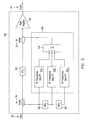
- FIG. 1 shows a linear power amplifier with an analog RF predistortion block.
- FIG. 2 shows the power detector described in FIG. 1 .
- FIG. 3 shows the envelop detector described in FIG. 1 .
- FIG. 4 shows the voltage response of a soft limiting amplifier that may be used in the RF predistortion block described in FIG. 1 .
- FIG. 5 shows the quadrature modulator described in FIG. 1 .
- FIG. 6 shows a digitally controlled analog subsystem of the RF predistortion block in FIG. 1 .
- FIG. 7 shows a memoryless polynomial block described in FIG. 6 .
- FIG. 8 shows a linear power amplifier with an analog RF predistortion block having off-chip delay elements.
- FIG. 9 shows a linear power amplifier with multiple analog RF predistortion blocks on a single integrated circuit.
- FIG. 10 shows a linear power amplifier with an analog RF predistortion block employing a feedback loop.
- FIG. 11 shows a telecommunications system with a linear power amplifier used to receive RF signals.
- FIG. 12 shows a telecommunications system with a linear power amplifier used to transmit RF signals.
- a linear PA circuit 100 is shown in FIG. 1 .
- RF Input signal 101 is injected into the circuit.
- An RF coupler 110 provides incoming RF input signal 101 to RF predistortion block 125 .
- RF input signal 101 may be a time-varying signal, expressed as x(t) 111 , which may have the form shown in Equ. 1, where r(t) is the envelope of the signal.
- x ( t ) r ( t )cos [2 ⁇ ft + ⁇ ( t )] Equ. 1
- RF distribution block 125 comprises envelop detector (EDet) 112 , power detector (PDet) 113 , digitally controlled analog subsystem (DCAS) 116 and quadrature modulator 120 .
- RF predistortion block 125 may be constructed as a single integrated circuit or as multiple integrated circuits or by discrete components, as desired.
- the envelope r(t) of x(t) 111 is output by envelop detector 112 as r(t) 114 .
- the power of x(t) 111 is output by power detector 113 as r 2 (t) 115 .
- the envelop and power of x(t) 111 , r(t) 114 and r 2 (t) 115 are input to DCAS 116 .
- DCAS 116 uses weights from coefficient vector generator 117 , DCAS 116 generates polynomials of r(t) 114 and r 2 (t) 115 .
- Coefficient vector generator 117 may create polynomial coefficients for DCAS 116 from a stored memory or by using an algorithm.
- the polynomials are represented by DCAS 116 as voltages V p (t) 118 and V q (t) 119 . Ignoring various nonidealities in the analog circuit implementation, these voltages may be expressed as shown in Equ. 2 and Equ. 3.
- a mk and b mk are polynomial coefficients and ⁇ k are memory delays.
- Polynomial coefficients a mk and b mk are provided by coefficient vector generator 117 .
- the voltages V p (t) 118 and V q (t) 119 are sent to quadrature modulator 120 , which also receives RF input signal x(t) 111 .
- Quadrature modulator 120 outputs a signal y(t) 121 .
- An RF coupler 130 couples the signal y(t) 121 into the input signal for PA 140 thus serving to predistort the original RF signal coming from RF input 101 . In this way, linearly amplified power is output from linear power amplifier 100 at RF output 141 .
- FIG. 2 describes one embodiment of the power detector 113 introduced in reference to FIG. 1 .
- Power detector 113 is a current-mode Gilbert multiplier 210 followed by a trans-impedance amplifier 220 shown with a loop that includes resistor 225 .
- FIG. 3 describes one embodiment of the envelop detector 112 introduced in reference to FIG. 1 . It is difficult to construct high-quality envelop detectors using diodes in standard CMOS because of the lack of diodes that can operate at RF frequencies such as, for example, 2.5 GHz. Other components are, therefore, typically better suited to certain RF applications.
- an envelop detector 112 comprises a limiting amplifier 305 preferably providing a bandwidth higher than the RF frequency of x(t) 111 and a small-signal gain of no less than 12 dB. Additional components of envelop detector 112 include a current-mode Gilbert multiplier 310 followed by a trans-impedance amplifier 320 shown with a loop that includes resistor 325 .
- An alternative technique for envelop detection is a power detector 113 followed by an analog square rooting circuit, which will operate with signals having bandwidths typically between 10 MHz to 50 MHz.
- an envelop detector is not required for the predistortion of many PAs.
- an approximate envelop detector followed by a soft limiting amplifier may be used.
- the SLA has a finite small-signal gain of about 15 dB.
- the SLA has a soft saturation behavior roughly comparable to a square-root function.
- FIG. 4 shows the SLA's nonlinear response in a piecewise linear approximation. Referring to FIG. 4 , the solid line is an example of the nonlinear voltage response of an SLA, and the dashed line is the square-root of the nonlinear voltage response.
- FIG. 5 describes one embodiment of the quadrature modulator 120 shown in FIG. 1 .
- the output voltages of the DCAS 116 , V p (t) and V q (t) are the input signals to quadrature modulator 120 .
- input signal x(t) 111 is rotated in rotator 501 to provide in-phase signal 510 and quadrature signal 520 , namely r(t)cos(2 ⁇ ft+ ⁇ (t)) and r(t)sin(2 ⁇ ft+ ⁇ (t)) respectively.
- the in-phase and quadrature signals are then respectively multiplied using multipliers 530 and 540 by V p (t) and V q (t) and added in summer 550 to provide output signal y(t) 121 .
- V p (t) and V q (t) have non-zero DC offsets
- the quadrature modulator 120 output, y(t) 121 may have a leakage of the RF input signal.
- any leakage will likely change the average input power of PA 140 .
- the DC offsets of V p (t) and V q (t) can be cancelled by either one of two techniques known to those working in the field. The first technique uses a negative feedback loop to cancel the DC offsets. A second technique uses capacitive coupling.
- FIG. 6 further describes DCAS 116 introduced in reference to FIG. 1 .
- Block 600 represents an example of a polynomial generator in DCAS 116 for generating a polynomial with a non-delayed and two delayed terms.
- the memory delays are 0, ⁇ , and 2 ⁇ .
- Delay elements 650 , 655 , 660 and 665 are analog delay components which may be implemented as first-order RC filters. As shown in FIG. 6 , these delay elements delay the envelope and power signals E(t) 601 and P(t) 602 , corresponding to envelope signal r(t) 114 and r 2 (t) 115 , for example.
- these delay components may be implemented as track-and-hold circuits where long delays can be achieved by cascading multiple track-and-hold stages.
- Memoryless polynomial circuits 700 a , 700 b and 700 c process the input signals E(t) 601 , P(t) 602 and from coefficient vectors 117 a , 117 b and 117 c , respectively.
- the output signals of circuits 700 a , 700 b and 700 c are sent to summer 670 and the resulting sum is output value V out 690 (i.e., generated V p (t) or V q (t)), after subtracted any detected offset value V os 680 .
- Equation 5 Equation 5
- Equation 6 Equation 6
- FIG. 7 describes a memoryless polynomial circuit 700 which can be used to implement any of memoryless polynomial circuits 700 a , 700 b and 700 c introduced in block 600 in FIG. 6 .
- Circuit 700 is a memoryless polynomial circuit with multipliers 705 - 707 , weights 710 - 714 and summer 720 .
- Weights 710 - 714 are the coefficients in a coefficient vector from coefficient vector generator 117 (not shown), e.g., any of coefficient vectors 117 a , 117 b and 117 c .
- Components of memoryless polynomial circuits 700 may be constructed with CMOS analog circuits.
- the total number of coefficients in DCAS 116 is reduced so that polynomial terms for r 2l+1 (t) for l ⁇ 1 are eliminated.
- the first-order envelope term is important to the predistortion of some PAs and is always preserved.
- the time-varying signal, V(t), can be expressed and implemented according to the following equation:
- r(t) is the envelop signal
- N is a predetermined integer greater than or equal to 2
- r 2j (t) are exponentials of the envelop signal
- a 2j are weights from the coefficient vector input signal.
- linear PA 800 In a second embodiment of a linear power amplifier, a linear PA 800 is shown in FIG. 8 .
- linear PA 800 further comprises RF delay elements RFD 1 810 and RFD 2 820 , where each delay is typically between 5 ns to 15 ns. If the RF predistortion block 125 is implemented as an integrated circuit, the memory compensation capability can be significantly improved by using off-chip RF delay elements RFD 1 810 and RFD 2 820 in the form of transmission lines.
- RFD 1 810 and RFD 2 820 can each provide suitable transmission delays (e.g., 4 ns), such that the delayed terms in RF predistortion block 125 may provide non-causal (i.e., negative valued, relative the delays of RFD 1 ) predistortion terms.
- a linear PA 900 is shown in FIG. 9 .
- Linear PA 900 employs at least three RF predistortion blocks 125 a , 125 b and 125 c connected in parallel, as described in reference to FIG. 1 .
- RF predistortion blocks 125 a , 125 b and 125 c may all reside on a single chip integrated circuit 980 .
- Linear PA 900 further comprises a combiner 970 connected to RF predistortion blocks 125 a , 125 b and 125 c that sums together the signals emanating from the quadrature modulators in each block.
- Linear PA 900 further comprises RF delay elements 910 , 920 and 930 .
- linear power amplifier 900 is suitable for high power Doherty amplifiers.
- Linear Amplifier 900 provides many options to fine tune the required predistortion to achieve a desired linear output profile.
- Linear PA 1000 belongs to class of linear power amplifiers that employ adaptive predistortion using one or more feedback loops.
- Linear PA 1000 comprises at least two predistortion blocks 125 a and 125 b , as described in reference to FIG. 1 .
- the at least two predistortion blocks 125 a and 125 b are connected in parallel and the output signals from these blocks are summed in summer 1300 .
- Predistortion block 125 b has a feedback signal returning from the output of PA 140 via coupler 1500 that is used for performance monitoring and coefficient adaptation.
- Predistortion blocks 125 a and 125 b and summer 1300 may be implemented on a single chip integrated circuit 1400 .
- FIG. 11 shows an embodiment of a telecommunications system 1100 .
- System 1100 comprises an RF receiving antenna 1110 , an RF linear power amplifier 100 as previously described herein, an RF receiving mixer 1130 , an RF receiving oscillator 1140 and an RF receiver 1150 .
- FIG. 12 shows an embodiment of a telecommunications system 1200 .
- System 1200 comprises an RF transmitter 1210 , an RF transmitting mixer 1220 , an RF transmitting oscillator 1230 , an RF linear power amplifier 100 as previously described herein and an RF transmitting antenna 1250 .
Abstract
Description
x(t)=r(t)cos [2πft+φ(t)] Equ. 1
In Equ. 2 and Equ. 3, amk and bmk are polynomial coefficients and πk are memory delays. Polynomial coefficients amk and bmk are provided by coefficient vector generator 117. The voltages Vp(t) 118 and Vq(t) 119 are sent to
y(t)=V p(t)r(t)cos [2πft+φ(t)]+V q(t)r(t)sin [2πft+φ(t)] Equ. 4
P(t)=r 2(t) Equ. 5
E(t)=√{square root over (P(t))} Equ. 6
V(t)=a 1 r(t)+a 2 r 2(t)+a 4 r 4(t)+a 6 r 6(t)+a 8 r 8(t) Equ. 7
where r(t) is the envelop signal, N is a predetermined integer greater than or equal to 2, r2j(t) are exponentials of the envelop signal, and a2j are weights from the coefficient vector input signal.
Claims (22)
y(t)=V p(t)r(t)cos [2πft+φ(t)]+V q(t)r(t)sin [2πft+φ(t)] (3)
V(t)=a 1 r(t)+a 2 r 2(t)+a 4 r 4(t)+a 6 r 6(t)+a 8 r 8(t) (5)
Priority Applications (1)
| Application Number | Priority Date | Filing Date | Title |
|---|---|---|---|
| US12/939,067 US8331487B2 (en) | 2010-11-03 | 2010-11-03 | Analog signal processor for nonlinear predistortion of radio-frequency signals |
Applications Claiming Priority (1)
| Application Number | Priority Date | Filing Date | Title |
|---|---|---|---|
| US12/939,067 US8331487B2 (en) | 2010-11-03 | 2010-11-03 | Analog signal processor for nonlinear predistortion of radio-frequency signals |
Publications (2)
| Publication Number | Publication Date |
|---|---|
| US20120106600A1 US20120106600A1 (en) | 2012-05-03 |
| US8331487B2 true US8331487B2 (en) | 2012-12-11 |
Family
ID=45996742
Family Applications (1)
| Application Number | Title | Priority Date | Filing Date |
|---|---|---|---|
| US12/939,067 Active 2031-04-08 US8331487B2 (en) | 2010-11-03 | 2010-11-03 | Analog signal processor for nonlinear predistortion of radio-frequency signals |
Country Status (1)
| Country | Link |
|---|---|
| US (1) | US8331487B2 (en) |
Cited By (4)
| Publication number | Priority date | Publication date | Assignee | Title |
|---|---|---|---|---|
| US20140009228A1 (en) * | 2011-08-03 | 2014-01-09 | Scintera Networks, Inc. | Pre-distortion for fast power transient waveforms |
| US9484962B1 (en) * | 2015-06-05 | 2016-11-01 | Infineon Technologies Ag | Device and method for adaptive digital pre-distortion |
| US10361730B2 (en) | 2016-04-18 | 2019-07-23 | Rohde & Schwarz Gmbh & Co. Kg | Amplifier device for high frequency signals |
| US10382073B2 (en) | 2015-11-03 | 2019-08-13 | Infineon Technologies Ag | Analog RF pre-distorter and non-linear splitter |
Families Citing this family (6)
| Publication number | Priority date | Publication date | Assignee | Title |
|---|---|---|---|---|
| US8805304B2 (en) * | 2011-10-25 | 2014-08-12 | Scintera Networks Llc | Linearization of broadband power amplifiers |
| US9036734B1 (en) * | 2013-07-22 | 2015-05-19 | Altera Corporation | Methods and apparatus for performing digital predistortion using time domain and frequency domain alignment |
| JP6501323B2 (en) * | 2014-11-14 | 2019-04-17 | 華為技術有限公司Huawei Technologies Co.,Ltd. | Analog predistorter core module and analog predistorter system |
| RU2623807C1 (en) * | 2016-06-09 | 2017-06-29 | Акционерное общество "Российская корпорация ракетно-космического приборостроения и информационных систем" (АО "Российские космические системы") | Digital device for preventing radio signals by even harmonics |
| TWI696344B (en) * | 2018-11-16 | 2020-06-11 | 財團法人工業技術研究院 | Linearity improving system and linearity improving method |
| RU2726184C1 (en) * | 2019-11-25 | 2020-07-09 | Акционерное общество "Концерн "Созвездие" | Pre-distorted signal generation method |
Citations (2)
| Publication number | Priority date | Publication date | Assignee | Title |
|---|---|---|---|---|
| US7804359B1 (en) * | 2008-10-23 | 2010-09-28 | Scintera Networks, Inc. | Linearization with memory compensation |
| US8121560B1 (en) * | 2008-10-23 | 2012-02-21 | Scintera Networks, Inc. | Pre-distortion with enhanced convergence for linearization |
-
2010
- 2010-11-03 US US12/939,067 patent/US8331487B2/en active Active
Patent Citations (2)
| Publication number | Priority date | Publication date | Assignee | Title |
|---|---|---|---|---|
| US7804359B1 (en) * | 2008-10-23 | 2010-09-28 | Scintera Networks, Inc. | Linearization with memory compensation |
| US8121560B1 (en) * | 2008-10-23 | 2012-02-21 | Scintera Networks, Inc. | Pre-distortion with enhanced convergence for linearization |
Cited By (5)
| Publication number | Priority date | Publication date | Assignee | Title |
|---|---|---|---|---|
| US20140009228A1 (en) * | 2011-08-03 | 2014-01-09 | Scintera Networks, Inc. | Pre-distortion for fast power transient waveforms |
| US9077299B2 (en) * | 2011-08-03 | 2015-07-07 | Scintera Networks Llc | Pre-distortion for fast power transient waveforms |
| US9484962B1 (en) * | 2015-06-05 | 2016-11-01 | Infineon Technologies Ag | Device and method for adaptive digital pre-distortion |
| US10382073B2 (en) | 2015-11-03 | 2019-08-13 | Infineon Technologies Ag | Analog RF pre-distorter and non-linear splitter |
| US10361730B2 (en) | 2016-04-18 | 2019-07-23 | Rohde & Schwarz Gmbh & Co. Kg | Amplifier device for high frequency signals |
Also Published As
| Publication number | Publication date |
|---|---|
| US20120106600A1 (en) | 2012-05-03 |
Similar Documents
| Publication | Publication Date | Title |
|---|---|---|
| US8331487B2 (en) | Analog signal processor for nonlinear predistortion of radio-frequency signals | |
| US20200358640A1 (en) | Modulation agnostic digital hybrid mode power amplifier system and method | |
| KR101107866B1 (en) | An uncorrelated adaptive predistorter | |
| US8588332B2 (en) | Dynamic digital pre-distortion system | |
| US7689180B2 (en) | Method and apparatus for a cartesian error feedback circuit to correct distortion within a power amplifier | |
| US6963242B2 (en) | Predistorter for phase modulated signals with low peak to average ratios | |
| EP1104093A1 (en) | Method and apparatus for generation of a RF signal | |
| KR20130126889A (en) | Semiconductor device | |
| JP6827613B2 (en) | Pre-distortion in satellite signal transmission systems | |
| US9124225B2 (en) | Dual power amplifier linearizer | |
| Qian et al. | A general adaptive digital predistortion architecture for stand-alone RF power amplifiers | |
| JP2019533327A (en) | Load modulation in signal transmission | |
| CN101233683B (en) | Data processing method, transmitter, device, network element and base station | |
| KR20020001834A (en) | Communication system with predistortion | |
| US10630323B2 (en) | Asymmetric adjacent channel leakage ratio (ACLR) control | |
| US9543911B2 (en) | Phase-modulated load apparatus and method | |
| Kumar et al. | Bandlimited DPD adapted APD for 5G communication | |
| US20080290939A1 (en) | Method and apparatus for distortion correction of RF amplifiers | |
| JP2007295331A (en) | Radio base station device | |
| Ceylan | Linearization of power amplifiers by means of digital predistortion | |
| Fujioka et al. | Power-amplifier-inserted transversal filter for application to pulse-density-modulation switching-mode transmitters | |
| Collados et al. | A low-current digitally predistorted 3G-4G transmitter in 40nm CMOS | |
| An et al. | An 8 Gbps E-band QAM transmitter using symbol-based outphasing power combining technique | |
| Patel | Adaptive digital predistortion linearizer for power amplifiers in military UHF satellite | |
| GB2394145A (en) | An isolator for a wireless communication unit |
Legal Events
| Date | Code | Title | Description |
|---|---|---|---|
| AS | Assignment |
Owner name: SCINTERA NETWORKS, INC., CALIFORNIA Free format text: ASSIGNMENT OF ASSIGNORS INTEREST;ASSIGNORS:YU, QIAN;ROGER, FREDERIC;BROADWELL, ADRIC Q.;AND OTHERS;REEL/FRAME:025244/0430 Effective date: 20101018 |
|
| STCF | Information on status: patent grant |
Free format text: PATENTED CASE |
|
| AS | Assignment |
Owner name: SCINTERA NETWORKS LLC, DELAWARE Free format text: CHANGE OF NAME;ASSIGNOR:SCINTERA NETWORKS, INC.;REEL/FRAME:033047/0864 Effective date: 20140505 |
|
| FPAY | Fee payment |
Year of fee payment: 4 |
|
| CC | Certificate of correction | ||
| FEPP | Fee payment procedure |
Free format text: MAINTENANCE FEE REMINDER MAILED (ORIGINAL EVENT CODE: REM.); ENTITY STATUS OF PATENT OWNER: SMALL ENTITY |
|
| FEPP | Fee payment procedure |
Free format text: 7.5 YR SURCHARGE - LATE PMT W/IN 6 MO, SMALL ENTITY (ORIGINAL EVENT CODE: M2555); ENTITY STATUS OF PATENT OWNER: SMALL ENTITY |
|
| MAFP | Maintenance fee payment |
Free format text: PAYMENT OF MAINTENANCE FEE, 8TH YR, SMALL ENTITY (ORIGINAL EVENT CODE: M2552); ENTITY STATUS OF PATENT OWNER: SMALL ENTITY Year of fee payment: 8 |