US8416022B2 - Power amplifier device - Google Patents
Power amplifier device Download PDFInfo
- Publication number
- US8416022B2 US8416022B2 US13/450,184 US201213450184A US8416022B2 US 8416022 B2 US8416022 B2 US 8416022B2 US 201213450184 A US201213450184 A US 201213450184A US 8416022 B2 US8416022 B2 US 8416022B2
- Authority
- US
- United States
- Prior art keywords
- inductor
- power amplifier
- ground pattern
- transistors
- amplifier device
- Prior art date
- Legal status (The legal status is an assumption and is not a legal conclusion. Google has not performed a legal analysis and makes no representation as to the accuracy of the status listed.)
- Expired - Fee Related
Links
Images


Classifications
-
- H—ELECTRICITY
- H03—ELECTRONIC CIRCUITRY
- H03F—AMPLIFIERS
- H03F3/00—Amplifiers with only discharge tubes or only semiconductor devices as amplifying elements
- H03F3/45—Differential amplifiers
- H03F3/45071—Differential amplifiers with semiconductor devices only
- H03F3/45076—Differential amplifiers with semiconductor devices only characterised by the way of implementation of the active amplifying circuit in the differential amplifier
- H03F3/45179—Differential amplifiers with semiconductor devices only characterised by the way of implementation of the active amplifying circuit in the differential amplifier using MOSFET transistors as the active amplifying circuit
- H03F3/45183—Long tailed pairs
-
- H—ELECTRICITY
- H03—ELECTRONIC CIRCUITRY
- H03F—AMPLIFIERS
- H03F3/00—Amplifiers with only discharge tubes or only semiconductor devices as amplifying elements
- H03F3/189—High frequency amplifiers, e.g. radio frequency amplifiers
- H03F3/19—High frequency amplifiers, e.g. radio frequency amplifiers with semiconductor devices only
- H03F3/195—High frequency amplifiers, e.g. radio frequency amplifiers with semiconductor devices only in integrated circuits
-
- H—ELECTRICITY
- H03—ELECTRONIC CIRCUITRY
- H03F—AMPLIFIERS
- H03F2203/00—Indexing scheme relating to amplifiers with only discharge tubes or only semiconductor devices as amplifying elements covered by H03F3/00
- H03F2203/45—Indexing scheme relating to differential amplifiers
- H03F2203/45352—Indexing scheme relating to differential amplifiers the AAC comprising a combination of a plurality of transistors, e.g. Darlington coupled transistors
-
- H—ELECTRICITY
- H03—ELECTRONIC CIRCUITRY
- H03F—AMPLIFIERS
- H03F2203/00—Indexing scheme relating to amplifiers with only discharge tubes or only semiconductor devices as amplifying elements covered by H03F3/00
- H03F2203/45—Indexing scheme relating to differential amplifiers
- H03F2203/45364—Indexing scheme relating to differential amplifiers the AAC comprising multiple transistors parallel coupled at their gates and sources only, e.g. in a cascode dif amp, only those forming the composite common source transistor
-
- H—ELECTRICITY
- H03—ELECTRONIC CIRCUITRY
- H03F—AMPLIFIERS
- H03F2203/00—Indexing scheme relating to amplifiers with only discharge tubes or only semiconductor devices as amplifying elements covered by H03F3/00
- H03F2203/45—Indexing scheme relating to differential amplifiers
- H03F2203/45731—Indexing scheme relating to differential amplifiers the LC comprising a transformer
Definitions
- the present invention relates to a power amplifier device that amplifies an input signal to a required voltage level.
- Patent document 1 discloses a distributed power amplifier device for amplifying a radio frequency (RF) signal efficiently and at low cost.
- the power amplifier device comprises a plurality of push-pull amplifiers which are coupled on another to form a circular geometry. Input signals of equal amplitude but with opposite phases are input to adjacent amplifiers (transistors) in each push-pull amplifier. A closed loop formed by coupling the plurality of push-pull amplifiers functions as a primary winding.
- the power amplifier device further comprises a secondary winding adapted to the geometry of the primary winding. The secondary winding combines power output by each of the push-pull amplifiers efficiently.
- the transistors are arranged in regions outside of the transformer.
- a total of the areas for installing the transistors become large.
- the above arrangement encounters a problem in which the chip area occupied by the enter power amplifier device becomes large.
- An object of this invention is to provide a power amplifier device of a type that combines the outputs of a plurality of transistor pairs which operate differentially, the power amplifier device satisfying both of delivering a high output and reducing the chip area occupied by the device.
- a power amplifier device formed over a substrate comprises a primary inductor, a ground pattern, a plurality of transistor pairs, and a secondary inductor.
- the primary inductor comprises a plurality of inductor elements arranged in a generally circular geometry, when viewed from a direction perpendicular to the substrate.
- the ground pattern is provided to extend from a portion of a region inside the primary inductor which is circular into regions outside the primary inductor, when viewed from the direction perpendicular to the substrate, and grounded at a plurality of points in the regions outside the primary inductor.
- Each of the plurality of transistor pairs is provided for linking with each of the plurality of inductor elements.
- first main electrodes of first and second transistors forming a transistor pair in linkage with the inductor element are coupled respectively.
- Second main electrodes of the first and second transistors are coupled to the ground pattern in the region inside the primary inductor and have electrical conduction to the respective plurality of points.
- First and second signals in a pair as differential input signals are supplied to control electrodes of the first and second transistors, respectively.
- the secondary inductor which comprises one turn of winding or multiple turns of winding is provided circularly so as to surround the primary inductor and further combines and outputs combined signals of the first and second signals combined in each of the inductor elements by magnetically coupling to the primary inductor.
- a plurality of transistor pairs are disposed in a region inside a transformer comprised of primary and secondary inductors or a region where a portion of the transistor pairs overlap with these inductors.
- the chip area occupied by the power amplifier device can be made smaller than that occupied by a comparable power amplifier known heretofore.
- the ground pattern coupled to the second electrodes of the transistors is grounded at a plurality of points in regions outside the transformer. In consequence, it is possible to reduce parasitic resistances and parasitic inductances in the paths between the second electrodes and the ground nodes. A decrease in the output of the power amplifier device can be prevented.
- FIG. 1 is a circuit diagram showing a transformer-based power amplifier in which n stages of transformers with a turn ratio of 1:m are coupled together;
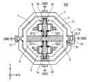
- FIG. 2 is a plan view showing a configuration of a power amplifier device 300 according to a first embodiment of this invention
- FIGS. 3(A) , 3 (B), and 3 (C) are plan views showing each of the components of the power amplifier device 300 in FIG. 2 .
- FIG. 4 is a plan view showing a primary inductor 104 part extracted from FIG. 3(A) ;
- FIG. 5 is a schematic cross-sectional diagram to explain the cross-section structure of the power amplifier device 300 shown in FIG. 2 ;
- FIGS. 6(A) and 6(B) are plan views showing the structure of a transistor Q 1 p in greater detail.
- FIG. 7 is an equivalent circuit diagram for the power amplifier device 300 in FIG. 2 ;
- FIG. 8 is a diagram showing a configuration of a power amplifier device 300 A as a first comparison example against the first embodiment
- FIG. 9 is a diagram showing a configuration of a power amplifier device 300 B as a second comparison example against the first embodiment
- FIG. 10 is a circuit diagram showing a configuration of a power amplifier device as a first example of modification to the first embodiment
- FIG. 11 is a plan view showing a ground pattern 102 a as a second example of modification to the first embodiment.
- FIG. 12 is a plan view showing a ground pattern 102 b as a third example of modification to the first embodiment.
- FIG. 13 is a plan view showing a configuration of a power amplifier device 301 according to a second embodiment of this invention.
- FIG. 14 is a plan view showing a primary inductor part extracted from FIG. 13 ;
- FIG. 15 is a plan view showing a ground pattern part extracted from FIG. 13 ;
- FIG. 16 is a plan view showing a configuration of a ground pattern 202 a as an example of modification to the ground pattern 202 in FIG. 15 ;
- FIG. 17 is a plan view showing a configuration of a ground pattern 202 b as another example of modification to the ground pattern 202 in FIG. 15 ;
- FIG. 18 is a plan view showing a configuration of a power amplifier device 302 according to a first example of modification to the second embodiment of this invention.
- FIG. 19 is a plan view showing a primary inductor part extracted from FIG. 18 ;
- FIG. 20 is a plan view showing a ground pattern part extracted from FIG. 18 ;
- FIG. 21 is a plan view showing a configuration of a ground pattern 212 a as an example of modification to the ground pattern 212 in FIG. 20 ;
- FIG. 22 is a plan view showing a configuration of a ground pattern 212 b as another example of modification to the ground pattern 212 in FIG. 20 ;
- FIG. 23 is a plan view showing a configuration of a power amplifier device 303 according to a second example of modification to the second embodiment of this invention.
- FIG. 24 is a plan view showing a configuration of a power amplifier device 304 according to a third embodiment of this invention.
- FIG. 25 shows a ground pattern 150 extracted from FIG. 24 ;
- FIGS. 26(A) and 26(B) are diagrams to further explain the effect of the ground pattern 150 in FIG. 25 ;
- FIG. 27 is a plan view showing a configuration of a ground pattern 150 a as an example of modification to the ground pattern in FIG. 25 ;
- FIGS. 28(A) , 28 (B), and 28 (C) are plan views showing a configuration of a power amplifier device as a second example of modification of the third embodiment of this invention.
- FIG. 29 is a plan view showing a configuration of a power amplifier device 306 according to a fourth embodiment of this invention.
- FIG. 30 is a plan view showing a ground pattern 109 part extracted from FIG. 29 .
- FIG. 1 is a circuit diagram showing a transformer-based power amplifier in which n stages of transformers with a turn ration of 1:m are coupled together.
- the transformer-based power amplifier includes n pieces (n is an integer of 2 or more) of transformers XF 1 to XFn and n pairs of transistors (AP 1 , AN 1 ) to (APn, ANn), each pair being provided for linking with each of the transformers XF 1 to XFn.
- Transistors AP, AN in each pair are respectively coupled to both ends of a primary winding of a transformer XF in linkage with the pair. Secondary windings of the transformers XF 1 to XFn are coupled in series to a load resistance RL.
- Each amplifier pair AP, AN is comprised of source-grounded NMOS (N-channel Metal Oxide Semiconductor) transistors (N-channel insulated gate field effect transistors).
- the amplifier pair AP, AN may also referred to as a transistor pair AP, AN.
- differential signals i.e., two signals having the same amplitude, but opposite phases IN+, IN ⁇ (first and second signals) are input.
- the output voltage of the transistors can be made to 1/(2 nm) by coupling the n stages of transformers XF with a turn ratio of 1:m.
- the output voltage amplitude (zero to peak) of the transformers XF 1 to XFn whose secondary windings are coupled in series is 20V.
- the voltage amplitude at the drain of each transistor becomes 10/mn V.
- the transformer-based power amplifier becomes a useful means for realizing a power amplifier device delivering output power in the order of several watts by a micro CMOS process.
- FIG. 2 is a plan view showing a configuration of a power amplifier device 300 according to a first embodiment of this invention.
- the power amplifier device 300 shown in FIG. 2 is formed over a substrate and includes a primary inductor (denoted by a reference numeral 104 in FIG. 3 ) comprised of inductor elements 1 , 2 , a secondary inductor 3 , a ground pattern (denoted by a reference numeral 102 in FIG. 3 ), and two pairs of transistors (Q 1 p , Q 1 n ) and (Q 2 p , Q 2 n ).
- a plane that is parallel to the substrate is assumed as an XY plane and a direction that is vertical to the substrate is assumed as a Z direction.
- To discriminate between two directions along the coordinate axis they are marked with positive and negative signs, such as +Z direction and ⁇ Z direction.
- FIGS. 3(A) , 3 (B), and 3 (C) are plan views showing each of the components of the power amplifier device 300 in FIG. 2 .
- FIG. 3(A) is a plan view of a transformer 101 comprised of the primary inductor 104 and the secondary inductor 3 .
- FIG. 3(B) is a plan view of the ground pattern 102 .
- FIG. 3(C) is a diagram schematically illustrating an arrangement of the transistor pairs Q 1 p , Q 1 n and Q 2 p , Q 2 n (which are generically referred to as an amplifier 103 ).
- each transformer is assumed to have a turn ratio of 1:1 and two stages are assumed to be coupled together.
- FIG. 4 is a plan view showing the primary inductor 104 part extracted from FIG. 3(A) .
- the primary inductor 104 is comprised of inductor elements 1 , 2 arranged in a generally circular geometry around a central axis CP that is vertical to the substrate.
- the entire form of the primary inductor 104 is two-turn symmetrical around the central axis CP and mirror symmetrical with respect to each of a symmetry plane 9 and a symmetry plane 10 which are both parallel to an XZ plane.
- One end 1 p of an inductor element 1 and one end 2 n of an inductor element 2 are disposed close to each other across the symmetry plane 10 and the other end 1 n of the inductor element 1 and the other end 2 p of the inductor element 2 are disposed close to each other across the symmetry plane 10 .
- the secondary inductor 3 is arranged circularly so as to surround the primary inductor 104 .
- the secondary inductor 3 produces a combined output of signals which have been input to the inductor elements by magnetically coupling to the primary inductor 104 .
- differential signals are output from both ends 3 p , 3 n of the secondary inductor 3 .
- one end 3 n is grounded and a single phase output signal OUT is output from the other end 3 p .
- the end 3 n may be grounded by coupling it to the ground pattern 102 via a contact hole e.
- the secondary inductor 3 shown in FIG. 2 and FIG. 3(A) has one turn of winding, it may have multiple turns of winding.
- the ground pattern 102 includes wiring portions 4 to 7 and a junction portion 8 .
- a wiring portion 4 extends from the vicinity of the central axis CP in an X direction along the symmetry plane 9 in FIG. 4 and into a region outside of the transformer 101 and its end terminal is grounded.
- a wiring portion 5 extends from the vicinity of the central axis CP in a Y direction along the symmetry plane 10 in FIG. 4 and into a region outside of the transformer 101 and its end terminal is grounded.
- a wiring portion 6 extends from the vicinity of the central axis CP in the X direction along the symmetry plane 9 in FIG. 4 and into a region outside of the transformer 101 and its end terminal is grounded.
- a wiring portion 7 extends from the vicinity of the central axis CP in the Y direction along the symmetry plane 10 in FIG. 4 and into a region outside of the transformer 101 and its end terminal is grounded.
- the junction portion 8 is provided in the vicinity of the central axis CP and joins the wiring portions 4 to 7 .
- the transistors Q 1 p , Q 1 n , Q 2 p , Q 2 n are embodied by NMOS transistors and arranged inside the rim of the transformer 101 , when viewed from the direction perpendicular to the substrate. When viewed from the direction perpendicular to the substrate, the wiring of the transformer 101 and each transistor may partially overlap.
- the transistors forming the transistor pairs are not limited to NMOS transistors; however, they may be, for example, bipolar transistors. Concrete coupling of each transistor is as below.
- a drain electrode 1 pd of a transistor Q 1 p is coupled to the end 1 p of the inductor element 1 via a contract hole f and a source electrode 1 ps thereof is coupled to the junction portion 8 via a contact hole a.
- a drain electrode 1 nd of a transistor Q 1 n is coupled to the end in of the inductor element 1 via a contract hole g and a source electrode ins thereof is coupled to the junction portion 8 via a contact hole b.
- a drain electrode 1 pd of a transistor Q 2 p is coupled to the end 2 p of the inductor element 2 via a contract hole h and a source electrode 2 ps thereof is coupled to the junction portion 8 via a contact hole c.
- a drain electrode 2 nd of a transistor Q 2 n is coupled to the end 2 n of the inductor element 2 via a contract hole i and a source electrode 2 ns thereof is coupled to the junction portion 8 via a contact hole d.
- a DC bias voltage is supplied to each transistor pair via the inductor element in linkage with the transistor pair. Specifically, as shown in FIG. 2 , a DC bias voltage Vd which is supplied to the transistors Q 1 P, Q 1 n is applied to a center tap 1 c in the vicinity of a midpoint of the inductor element 1 . A DC bias voltage Vd which is supplied to the transistors Q 2 P, Q 2 n is applied to a center tap 2 c in the vicinity of a midpoint of the inductor element 2 .
- Input signals IN+, IN ⁇ as differential input signals are input to the gate electrodes of the transistors Q 1 P, Q 1 n and to the gate electrodes of the transistors Q 2 P, Q 2 n , respectively.
- the input signals IN+, IN ⁇ are amplified by the transistors Q 1 P, Q 1 n and then combined by the inductor element 1 .
- the input signals IN+, IN ⁇ are amplified by the transistors Q 2 P, Q 2 n and then combined by the inductor element 2 .
- the signals thus combined by the inductor elements 1 , 2 are further combined by the secondary inductor 3 and then output from the terminal 3 p.
- FIG. 5 is a schematic cross-sectional diagram to explain the cross-section structure of the power amplifier device 300 shown in FIG. 2 .
- the schematic cross-sectional diagram of FIG. 5 is intended to explain the locations of metal layers and the couplings via contact holes and does not exactly correspond to the plan view of FIG. 2 .
- the transistors Q 1 p , Q 1 n , Q 2 p , Q 2 n are formed using a first metal layer over the substrate SUB.
- the ground pattern 102 is formed using a second metal layer above the first metal layer.
- the transformer 101 is formed using a third metal later above the second metal layer.
- Contract holes a, b, c, d are formed to couple the transistors Q 1 p , Q 1 n , Q 2 p , Q 2 n and the ground pattern 102 .
- Contact holes f, g, h, i are formed to couple the transistors Q 1 p , Q 1 n , Q 2 p , Q 2 n and the inductor element 1 .
- openings 7 A, 5 A, 5 B, 7 B, as shown in FIG. 3(B) are formed to allow the contact holes f, g, h, i, to pass therethrough.
- FIGS. 6(A) and 6(B) are plan views showing the structure of a transistor Q 1 p in greater detail.
- FIG. 6(A) shows the locations of the drain electrode 1 pd , the source electrode fps, and the gate electrode 1 pg and
- FIG. 6(B) shows the locations of p-type impurity regions 74 , n-type impurity regions 75 , and a trench isolation region 73 on the surface of the substrate SUB.
- the p-type impurity regions 74 are used as channel regions of the NMOS transistor and the n-type impurity regions 75 are used as drain and source regions alternately.
- the structure of the transistor Q 1 p is shown as a representative; obviously, other transistors Q 1 n , Q 2 p , Q 2 n have the same structures as shown here.
- An aluminum wiring 70 forming the drain electrode 1 pd is coupled to the drain regions via a plurality of contact holes CT 2 .
- An aluminum wiring 71 forming the source electrode 1 ps is coupled to the source regions via a plurality of contact holes CT 1 .
- Aluminum wirings 71 which respectively form the source electrodes 1 ps of the transistors Q 1 p , Q 1 n , Q 2 p , Q 2 n in FIG. 2 may be formed to be inter-coupled together and unified.
- the gate electrode 1 pg includes a polysilicon layer 72 laminated on top of a gate insulating film over the channel regions and an aluminum wiring 77 coupled to the polysilicon layer 72 via a contact hole CT 3 .
- the aluminum wiring 77 is formed using the first metal layer as mentioned in FIG. 5 .
- the polysilicon layer is hatched in order to clarify the illustration.
- the chip area occupied by the power amplifier device can be made smaller than that occupied by a comparable power amplifier known heretofore by arranging the transistors Q 1 p , Q 1 n , Q 2 p , Q 2 n in an area inside the rim of the transformer 101 .
- the four wiring portions 4 to 7 provide parallel couplings between the source electrodes of the transistors Q 1 p , Q 1 n , Q 2 p , Q 2 n and the ground nodes GND. As a result, it is possible to reduce parasitic resistances and parasitic inductances in the paths from the source electrodes of the transistors to the ground nodes GND and a decrease in the output of the power amplifier device 300 can be inhibited.
- the wiring portions 4 to 7 forming the ground pattern 102 run though the mirror symmetry planes 9 , 10 in the primary inductor 104 as shown in FIG. 4 .
- the mirror symmetry planes 9 , 10 serve as virtual AC grounds in differential operation, the RF characteristic of the transformer 101 is less affected by the wiring portions 4 to 7 . Consequently, the width of the grounding wires can be made wider than in a case where the grounding wires are placed in other positions and it is possible to further reduce parasitic resistances in the paths from the ground terminals of the transistors to the grounds.
- the ground pattern 102 as a whole has a mirror symmetrical property nearly like the primary inductor 104 , an unbalanced differential operation is hard to take place.
- the advantageous effects of the power amplifier device 300 will be further described, while giving a concrete example and comparison examples.
- FIG. 7 is an equivalent circuit diagram for the power amplifier device 300 in FIG. 2 .
- the inductor element 1 and the transistor pair Q 1 p , Q 1 n coupled to it are shown.
- the on-resistance of the transistors Q 1 p , Q 1 n is denoted by Ron
- the resistance of the parallel wiring portions 4 to 7 from the junction portion 8 to the ground nodes GND is denoted by Rs
- the inductance of the parallel wiring portions is denoted by Ls.
- a DC voltage Vds drain-source voltage
- Vds Vd ⁇ ( R on/2) ⁇ ( R on/2 +Rs ).
- the parasitic inductance Ls of the grounding wires does not affect the DC voltage, but has an effect on the RF signal as impedance as large as ⁇ Ls (where ⁇ is an angular frequency).
- ⁇ Ls an angular frequency
- the parasitic inductance Ls has no effect on the output OUT of the power amplifier device 300 .
- differential input signals IN+, IN ⁇ are asymmetric, or if the characteristics of the transistors vary within the board surface, the differential operation of the power amplifier device will become unbalanced. In that event, it is possible to inhibit a decrease in the output OUT by making the parasitic inductance Ls as small as possible.
- FIG. 8 is a diagram showing a configuration of a power amplifier device 300 A as a first comparison example against the first embodiment.
- FIG. 8 an example is shown where the transistors Q 1 p , Q 1 n , Q 2 p , Q 2 n are arranged in an area outside the transformer 101 .
- the transistors Q 1 p , Q 1 n , Q 2 p , Q 2 n are often disposed outside the transformer, as shown in FIG. 8 .
- a common source electrode 81 of the transistors Q 1 p , Q 2 n can be coupled to a ground node GND via a boding wire 80 B and a common source electrode 82 of the transistors Q 1 n , Q 2 p can be coupled to a ground node GND via a bonding wire 80 A.
- the entire power amplifier device is designed to occupy a smaller chip area by disposing the transistors inside the transformer. Further, by providing the wiring portions 4 to 7 for grounding so as to be vertically mirror symmetrical with respect to the symmetry planes 9 , 10 , it is possible to make the parasitic resistances and parasitic inductances as small as possible.
- FIG. 9 is a diagram showing a configuration of a power amplifier device 300 B as a second comparison example against the first embodiment.
- FIG. 9 an example is shown where the transistors Q 1 p , Q 1 n , Q 2 p , Q 2 n are arranged in an area inside the transformer 101 .
- the junction portion 8 is coupled to a ground node GND by a single wiring portion 83 and a bonding wire 80 D.
- the wiring portion 83 has a parasitic resistance and a parasitic inductance that are at least four times as much as the total parasitic resistance and parasitic inductance of the wiring portions 4 to 7 in FIG. 2 . Further, the wiring portion 83 is placed so as not to be mirror symmetrical with respect to the symmetry planes 9 , 10 . Consequently, the output OUT will become lower than the output of the power amplifier device 300 according to the first embodiment.
- FIG. 10 is a circuit diagram showing a configuration of a power amplifier device as a first example of modification to the first embodiment.
- FIG. 10 an example is shown where differential pairs comprise n pairs of parallel transistors.
- the transistors for the inductor element 1 in FIG. 2 are shown, but the transistors for the inductor element 2 are assumed to be provided as shown here.
- the power amplifier device in FIG. 10 includes n pieces of transistors Q 1 p _ 1 to Q 1 p _n coupled in parallel between the end 1 p of the inductor element 1 and the junction portion 8 and a pieces of transistors Q 1 n _ 1 to Q 1 n _n coupled in parallel between the end 1 n thereof and the junction portion 8 .
- a first signal IN+ is input to the gate electrodes of the Q 1 p _ 1 to Q 1 p _n and a second signal IN ⁇ is input to the gate electrodes of the transistors Q 1 n _ 1 to Q 1 n _n.
- Vds drain-source voltage
- FIG. 11 is a plan view showing a ground pattern 102 a as a second example of modification to the first embodiment.
- the layout of the primary inductors 1 , 2 and secondary inductor 3 is also shown.
- the ground pattern 102 a may be configured with only the wiring portions 4 , 6 and the junction portion 8 along the mirror symmetry plane 9 in FIG. 4 .
- parasitic resistances and parasitic inductances in the paths between the junction portion 8 and the ground nodes GND become larger than in the case of FIG. 2 , but can be made smaller than in the case of the comparison example in FIG. 9 .
- FIG. 12 is a plan view showing a ground pattern 102 b as a third example of modification to the first embodiment.
- the layout of the primary inductors 1 , 2 and secondary inductor 3 is also shown.
- the ground pattern 102 b may be configured with only the wiring portions 5 , 7 and the junction portion 8 along the mirror symmetry plane 10 in FIG. 4 .
- parasitic resistances and parasitic inductances in the paths between the junction portion 8 and the ground nodes GND become larger than in the case of FIG. 2 , but can be made smaller than in the case of the comparison example in FIG. 9 .
- While the first embodiment has illustrated the example of the power amplifier device in which the transformer combines the outputs of two pairs of differentially operating transistors, the same function/effect can be achieved even if the number of pairs of such transistors is varied.
- FIG. 13 is a plan view showing a configuration of a power amplifier device 301 according to a second embodiment of this invention.
- the power amplifier device 301 as shown in FIG. 13 , provided over a substrate includes a primary inductor (denoted by a reference numeral 201 in FIG. 14 ) comprised of inductor elements 21 , 22 , 23 , a secondary inductor 20 , a ground pattern (denoted by a reference numeral 202 in FIG. 15 ), and three pairs of transistors (Q 1 p , Q 1 n ), (Q 2 p , Q 2 n ), (Q 3 p , Q 3 n ).
- FIG. 14 is a plan view showing the primary inductor part extracted from FIG. 13 .
- the primary inductor 201 is comprised of the inductor elements 21 , 22 , 23 arranged in a generally circular geometry around the central axis CP that is vertical to the substrate.
- the entire form of the primary inductor 201 is three-turn symmetrical around the central axis CP and mirror symmetrical with respect to each of symmetry planes 25 , 26 , 27 , each of which includes the central axis CP.
- FIG. 15 is a plan view showing the ground pattern part extracted from FIG. 13 .
- the ground pattern 202 includes wiring portions 25 a , 25 b , 26 a , 26 b , 27 a , 27 b , and a junction portion 24 .
- wiring portions 25 a , 25 b are laid along a symmetry plane 25 in FIG. 14 and coupled together in the junction portion 24 in the vicinity of the central axis CP in FIG. 14 .
- the wiring portions 25 a , 25 b are grounded respectively in regions outside of the circular primary inductor 201 ( 21 , 22 , 23 ).
- wiring portions 26 a , 26 b When viewed from the direction perpendicular to the substrate, wiring portions 26 a , 26 b are laid along a symmetry plane 26 in FIG. 14 and coupled together in the junction portion 24 . The wiring portions 26 a , 26 b are grounded respectively in regions outside of the circular primary inductor 201 .
- wiring portions 27 a , 27 b When viewed from the direction perpendicular to the substrate, wiring portions 27 a , 27 b are laid along a symmetry plane 27 in FIG. 14 and coupled together in the junction portion 24 . The wiring portions 27 a , 27 b are grounded respectively in regions outside of the circular primary inductor 201 . Openings like those shown in FIG.
- the ground pattern 202 has rotational symmetries with respect to the same rotational symmetry axis CP as for the primary inductor 201 and has mirror symmetries with respect to the same mirror symmetry planes 25 , 26 , 27 as for the primary inductor 201 .
- the secondary inductor 20 is arranged circularly so as to surround the primary inductor 201 ( 21 , 22 , 23 ).
- the secondary inductor 20 produces a combined output of signals which have been input to the inductor elements by magnetically coupling to the primary inductor 201 .
- differential signals are output from both ends 20 p , 20 n of the secondary inductor 20 .
- the power amplifier device 301 provides a single phase output
- one end 20 n is grounded and a single phase output signal OUT is output from the other end 20 p .
- the secondary inductor 20 shown in FIG. 13 has one turn of winding, it may have multiple turns of winding.
- Drain electrodes of transistors Q 1 p , Q 1 n are coupled to the ends 21 p , 21 n of the inductor element 21 , respectively, and source electrodes thereof are coupled to the junction portion (denoted by a reference numeral 24 in FIG. 15 ).
- First and second signals IN+, IN ⁇ as differential input signals are input to gate electrodes of the transistor pair Q 1 p , Q 1 n .
- a bias voltage Vd for the transistors Q 1 p , Q 1 n is applied to a center tap 21 c in the vicinity of a midpoint of the inductor element 21 .
- Drain electrodes of transistors Q 2 p , Q 2 n are coupled to the ends 22 p , 22 n of the inductor element 22 , respectively, and source electrodes thereof are coupled to the junction portion (denoted by the reference numeral 24 in FIG. 15 ).
- First and second signals IN+, IN ⁇ as differential input signals are input to gate electrodes of the transistor pair Q 2 p , Q 2 n .
- a bias voltage Vd for the transistors Q 2 p , Q 2 n is applied to a center tap 22 c in the vicinity of a midpoint of the inductor element 22 .
- Drain electrodes of transistors Q 3 p , Q 3 n are coupled to the ends 23 p , 23 n of the inductor element 23 , respectively, and source electrodes thereof are coupled to the junction portion (denoted by the reference numeral 24 in FIG. 15 ).
- First and second signals IN+, IN ⁇ as differential input signals are input to gate electrodes of the transistor pair Q 3 p , Q 3 n .
- a bias voltage Vd for the transistors Q 3 p , Q 3 n is applied to a center tap 23 c in the vicinity of a midpoint of the inductor element 23 .
- ground pattern 202 By the application of the ground pattern 202 , parasitic resistances and parasitic inductances in the paths from the source electrodes of the transistors to the ground nodes GND are reduced by a factor of 6, roughly, as compared with the comparison example in FIG. 9 .
- FIG. 16 is a plan view showing a configuration of a ground pattern 202 a as an example of modification to the ground pattern 202 in FIG. 15 .
- the layout of the primary inductor 201 21 , 22 , 23 ) is also shown.
- the ground pattern 202 a may be configured with only the wiring portions 25 a , 26 a , 27 a and the junction portion 24 in FIG. 14 .
- the entire form of the ground pattern 202 a is three-turn symmetrical with respect to the central axis CP in FIG. 14 and mirror symmetrical with respect to each of the symmetry planes 25 , 26 , 27 .
- parasitic resistances and parasitic inductances in the paths between the junction portion 24 and the ground nodes GND become double, as compared with the case of FIG. 13 , but can be made smaller than in the case of the comparison example in FIG. 9 .
- FIG. 17 is a plan view showing a configuration of a ground pattern 202 b as another example of modification to the ground pattern 202 in FIG. 15 .
- the layout of the primary inductor 201 21 , 22 , 23 ) is also shown.
- the ground pattern 202 b may be configured with only the wiring portions 25 b , 26 b , 27 b and the junction portion 24 in FIG. 14 .
- the entire form of the ground pattern 202 b is three-turn symmetrical with respect to the central axis CP in FIG. 14 and mirror symmetrical with respect to each of the symmetry planes 25 , 26 , 27 .
- parasitic resistances and parasitic inductances in the paths between the junction portion 24 and the ground nodes GND become double, as compared with the case of FIG. 13 , but can be made smaller than in the case of the comparison example in FIG. 9 .
- FIG. 18 is a plan view showing a configuration of a power amplifier device 302 according to a first example of modification to the second embodiment of this invention.
- the power amplifier device 302 shown in FIG. 18 is provided over the substrate and includes a primary inductor (denoted by a reference numeral 211 in FIG. 19 ) comprised of inductor elements 31 , 32 , 33 , 34 , a secondary inductor 30 , a ground pattern (denoted by a reference numeral 212 in FIG. 20 ), and four pairs of transistors (Q 1 p , Q 1 n ), (Q 2 p , Q 2 n ), (Q 3 p , Q 3 n ), (Q 4 p , Q 4 n ).
- FIG. 19 is a plan view showing the primary inductor part extracted from FIG. 18 .
- the primary inductor 211 is comprised of the inductor elements 31 , 32 , 33 , 34 arranged in a generally circular geometry around a central axis CP that is vertical to the substrate.
- the entire form of the primary inductor 211 is four-turn symmetrical around the central axis CP and mirror symmetrical with respect to each of symmetry planes 36 , 37 , 38 , 39 , each of which includes the central axis CP.
- FIG. 20 is a plan view showing the ground pattern part extracted from FIG. 18 .
- the ground pattern 212 includes wiring portions 36 a , 36 b , 37 a , 37 b , 38 a , 38 b , 39 a , 39 b and a junction portion 35 .
- wiring portions 36 a , 36 b are laid along a symmetry plane 36 in FIG. 19 and coupled together in the junction portion 35 in the vicinity of the central axis CP in FIG. 19 .
- the wiring portions 36 a , 36 b are grounded respectively in regions outside of the circular primary inductor 211 ( 31 , 32 , 33 , 34 ).
- wiring portions 37 a , 37 b are laid along a symmetry plane 37 in FIG. 19 and coupled together in the junction portion 35 .
- the wiring portions 37 a , 37 b are grounded respectively in regions outside of the circular primary inductor 211 .
- wiring portions 38 a , 38 b are laid along a symmetry plane 38 in FIG. 19 and coupled together in the junction portion 35 .
- the wiring portions 38 a , 38 b are grounded respectively in regions outside of the circular primary inductor 211 .
- wiring portions 39 a , 39 b are laid along a symmetry plane 39 in FIG.
- the wiring portions 39 a , 39 b are grounded respectively in regions outside of the circular primary inductor 211 . Openings like those shown in FIG. 3(B) are further provided in the wiring portions 36 a , 36 b , 37 a , 37 b , 38 a , 38 b , 39 a , 39 b in FIG. 20 , but the openings are omitted from the illustration here.
- the ground pattern 212 has mirror symmetries with respect to the same rotational symmetry axis CP and mirror symmetry planes 36 , 37 , 38 , 39 as for the primary inductor 211 .
- the secondary inductor 30 is arranged circularly so as to surround the primary inductor 211 ( 31 , 32 , 33 , 34 ).
- the secondary inductor 30 produces a combined output of signals which have been input to the inductor elements by magnetically coupling to the primary inductor 211 .
- differential signals are output from both ends 30 p , 30 n of the secondary inductor 30 .
- the power amplifier device 302 provides a single phase output
- one end 30 n is grounded and a single phase output signal OUT is output from the other end 30 p .
- the secondary inductor 30 shown in FIG. 18 has one turn of winding, it may have multiple turns of winding.
- Drain electrodes of transistors Q 1 p , Q 1 n are coupled to the ends 31 p , 31 n of the inductor element 31 , respectively, and source electrodes thereof are coupled to the junction portion (denoted by a reference numeral 35 in FIG. 20 ).
- First and second signals IN+, IN ⁇ as differential input signals are input to gate electrodes of the transistor pair Q 1 p , Q 1 n .
- a bias voltage Vd for the transistors Q 1 p , Q 1 n is applied to a center tap 31 c in the vicinity of a midpoint of the inductor element 31 .
- Drain electrodes of transistors Q 2 p , Q 2 n are coupled to the ends 32 p , 32 n of the inductor element 32 , respectively, and source electrodes thereof are coupled to the junction portion (denoted by the reference numeral 35 in FIG. 20 ).
- First and second signals IN+, IN ⁇ as differential input signals are input to gate electrodes of the transistor pair Q 2 p , Q 2 n .
- a bias voltage Vd for the transistors Q 2 p , Q 2 n is applied to a center tap 32 c in the vicinity of a midpoint of the inductor element 32 .
- Drain electrodes of transistors Q 3 p , Q 3 n are coupled to the ends 33 p , 33 n of the inductor element 33 , respectively, and source electrodes thereof are coupled to the junction portion (denoted by the reference numeral 35 in FIG. 20 ).
- First and second signals IN+, IN ⁇ as differential input signals are input to gate electrodes of the transistor pair Q 3 p , Q 3 n .
- a bias voltage Vd for the transistors Q 3 p , Q 3 n is applied to a center tap 33 c in the vicinity of a midpoint of the inductor element 33 .
- Drain electrodes of transistors Q 4 p , Q 4 n are coupled to the ends 34 p , 34 n of the inductor element 34 , respectively, and source electrodes thereof are coupled to the junction portion (denoted by the reference numeral 35 in FIG. 20 ).
- First and second signals IN+, IN ⁇ as differential input signals are input to gate electrodes of the transistor pair Q 4 p , Q 4 n .
- a bias voltage Vd for the transistors Q 4 p , Q 4 n is applied to a center tap 34 c in the vicinity of a midpoint of the inductor element 34 .
- ground pattern 212 By the application of the ground pattern 212 , parasitic resistances and parasitic inductances in the paths from the source electrodes of the transistors to the ground nodes GND are reduced by a factor of 8, roughly, as compared with the comparison example in FIG. 9 .
- FIG. 21 is a plan view showing a configuration of a ground pattern 212 a as an example of modification to the ground pattern 212 in FIG. 20 .
- the layout of the primary inductor 211 ( 31 , 32 , 33 , 34 ) is also shown.
- the ground pattern 212 a may be configured with only the wiring portions 36 a , 36 b , 38 a , 38 b and the junction portion 35 in FIG. 19 .
- the entire form of the ground pattern 212 a is four-turn symmetrical with respect to the central axis CP in FIG. 19 and mirror symmetrical with respect to each of the symmetry planes 36 , 37 , 38 , 39 .
- parasitic resistances and parasitic inductances in the paths between the junction portion 35 and the ground nodes GND become double, as compared with the case of FIG. 18 , but can be made smaller than in the case of the comparison example in FIG. 9 .
- FIG. 22 is a plan view showing a configuration of a ground pattern 212 b as another example of modification to the ground pattern 212 in FIG. 20 .
- the layout of the primary inductor 211 ( 31 , 32 , 33 , 34 ) is also shown.
- the ground pattern 212 b may be configured with only the wiring portions 37 a , 37 b , 39 a , 39 b and the junction portion 35 in FIG. 19 .
- the entire form of the ground pattern 212 b is four-turn symmetrical with respect to the central axis CP in FIG. 19 and mirror symmetrical with respect to each of the symmetry planes 36 , 37 , 38 , 39 .
- parasitic resistances and parasitic inductances in the paths between the junction portion 35 and the ground nodes GND become double, as compared with the case of FIG. 18 , but can be made smaller than in the case of the comparison example in FIG. 9 .
- FIG. 23 is a plan view showing a configuration of a power amplifier device 303 according to a second example of modification to the second embodiment of this invention.
- the power amplifier device 303 shown in FIG. 23 is provided over the substrate and includes a primary inductor 40 , a secondary inductor 41 , a ground pattern 43 , and one pair of transistors (Q 1 p , Q 1 n ).
- the primary inductor 40 is provided in a generally circular geometry around a central axis CP that is vertical to the substrate.
- the entire form of the primary inductor 40 is mirror symmetrical with respect to a symmetry plane 42 including the central axis CP.
- the ground pattern 43 is a wiring that is laid along the symmetry plane 42 , when viewed from the direction perpendicular to the substrate, and extends from an outside region at one side of the primary inductor 40 into an outside region at the opposite side thereof.
- the ground pattern 43 is grounded at both ends.
- the ground pattern 43 can be regarded as a structure in which two wiring portions along the symmetry plane 42 are coupled together in a junction portion in the vicinity of the central axis CP.
- the secondary inductor 41 is provided circularly so as to surround the primary inductor 40 .
- the secondary inductor 41 outputs a signal that has been input to the primary inductor 40 by magnetically coupling to the primary inductor 40 .
- differential signals are output from both ends 41 p , 41 n of the secondary inductor 41 .
- one end 41 n is grounded and a single phase output signal OUT is output from the other end 41 p .
- the primary inductor 40 and the secondary inductor 41 shown in FIG. 23 have one turn of winding, they may have multiple turns of winding.
- Drain electrodes of transistors Q 1 p , Q 1 n are coupled to the ends 40 p , 40 n of the primary inductor 40 , respectively, and source electrodes thereof are coupled to the ground pattern 43 .
- First and second signals IN+, IN ⁇ as differential input signals are input to gate electrodes of the transistor pair Q 1 p , Q 1 n .
- a bias voltage Vd for the transistors Q 1 p , Q 1 n is applied to a center tap 40 c in the vicinity of a midpoint of the primary inductor 40 .
- FIG. 24 is a plan view showing a configuration of a power amplifier device 304 according to a third embodiment of this invention.
- FIG. 25 shows a ground pattern 150 extracted from FIG. 24 .
- the ground pattern 150 is regarded as a patterned ground shield 150 formed by adding multiple open stubs (wring portions) 50 intersecting the transformer (primary inductors 1 , 2 and secondary inductor 3 ) at 45° or 90° to the ground pattern 102 shown in FIG. 3(B) .
- the entire form of the multiple open stubs (wiring portions) 50 is four-turn symmetrical around the central axis CP and mirror symmetrical with respect to the symmetry planes 9 , 10 of the primary inductor elements 1 , 2 shown in FIG. 4 .
- the overall size of the ground pattern 150 is somewhat larger than the size of the transformer, when viewed from the direction perpendicular to the substrate.
- the transistors Q 1 p , Q 1 n , Q 2 p , Q 2 n are disposed inside the transformer (primary inductors 1 , 2 and secondary inductor 3 ), it is a concern that electrically conducting parts (aluminum wiring leads and impurity regions) in the transistors are magnetically coupled to the wiring portions of the transformer due to the fact that the transistors are located in a zone into which magnetic fluxes of the transformer concentrate. Magnetic coupling between the transformer and the transistors causes an unexpected backward current which results in a decrease in the output of the power amplifier device.
- the transformer (primary inductors 1 , 2 and secondary inductor 3 ) and the transistors Q 1 p , Q 1 n , Q 2 p , Q 2 n are spatially separated by the patterned ground shield 150 and magnetic coupling between both is thus blocked to a certain extent.
- ground pattern 150 having the geometry as shown in FIG. 25 still maintains the effect of significantly reducing parasitic resistances and parasitic inductances in the paths from the source electrodes of the transistors to the ground nodes GND.
- the use of the patterned ground shield 150 has no small effect on the RF characteristic of the transformer, as compared with the case of the first embodiment.
- the use of such shield results in a decrease in substrate loss, that is, an increase of Q value and a decrease of self-resonant frequency of the inductors configuring the transformer.
- FIGS. 24 and 25 are the same as in FIGS. 2 and 3(A) thru 3 (C) and, therefore, same or corresponding parts are assigned the same reference designators and their description is not repeated.
- FIGS. 26(A) and 26(B) are diagrams to further explain the effect of the ground pattern 150 in FIG. 25 .
- FIG. 26(A) is a diagram showing a comparison example where a single monolithic shield film 150 is provided instead of the ground pattern 150 .
- FIG. 26(B) depicts the ground pattern 150 in FIG. 25 in contrast to the shield film 151 of FIG. 26(A) .
- a patterned ground shield is provided to inhibit coupling between an inductor (including a transformer) and a lossy substrate via an oxide film.
- an inductor including a transformer
- a large eddy current EC is generated in the shield film 151 by induced electromotive force and a large energy loss occurs. This is because it is impossible to realize a shield film completely fixed to a ground potential, due to the fact that the shield film 151 has a finite resistance.
- the shield film 151 cannot be used because of the energy loss.
- the patterned ground shield 150 is used, even though the magnetic shielding effect is weaker than the monolithic shield film 151 .
- the patterned ground shield 150 it is possible to inhibit a crosstalk via parasitic capacitances between the transformer (primary inductors 1 , 2 and secondary inductor 3 ) and the transistors Q 1 p , Q 1 n , Q 2 p , Q 2 n .
- This crosstalk inhibiting effect is significant, particularly when the transformer and the transistors are provided such that both are partially overlapping.
- the stubs (wiring portions) 50 it is preferable to orient the stubs (wiring portions) 50 to be orthogonal to the wiring parts (conductors) of the transformer (primary inductors 1 , 2 and secondary inductor 3 ), wherever possible, when viewed from the direction perpendicular to the substrate.
- the width of the stubs (wiring portions) 50 is too wide, the energy loss increases, because the effect of cutting off the path through which the eddy current flows is reduced.
- the width of the stubs (wiring portions) 50 is narrow, the parasitic resistances of the stubs increase. This increases the loss of an RF signal in the paths between the wiring parts (conductors) of the transformer and the ground nodes GND (that is, the paths from the wiring parts (conductors) of the transformer extending to the stubs (wiring portions) 50 by capacitance coupling and up to the ground nodes GND via the stubs (wiring portions) 50 ). In consequence, this weakens the effect of inhibiting the crosstalk via parasitic capacitance between the transformer and the transistors. Therefore, an optimal width of the stubs (wiring portions) 50 should be selected.
- the width of the slits 55 should usually be narrower in order to increase the proportion of covering the transformer with the shield.
- the number of the stubs is determined by an area required to cover the transformer to a sufficient extent, an optimal width of the stubs, and a minimum gap between two stubs determined by a design rule.
- FIG. 27 is a plan view showing a configuration of a ground pattern 150 a as an example of modification to the ground pattern in FIG. 25 .
- the geometry of the ground pattern 150 a in FIG. 27 is the same as the ground pattern 150 in FIG. 25 , but there is a difference in coupling to ground nodes GND.
- the ends of wiring portions 51 , 52 , 53 , 54 coupled together in the junction portion 8 are further grounded. Thereby, it is possible to further reduce parasitic resistances and parasitic inductances in the paths between the source electrodes of the transistors Q 1 p , Q 1 n , Q 2 p , Q 2 n and the ground nodes GND. More ground points may be provided and the ends of all wiring portions 50 may be grounded.
- FIGS. 28(A) , 28 (B), and 28 (C) are plan views showing a configuration of a power amplifier device as a second example of modification of the third embodiment of this invention.
- FIG. 28(A) shows the configuration of a transformer 106 comprised of primary inductors 1 , 2 and secondary inductor 3 .
- the configuration of the transformer 106 is the same as the transformer 101 in FIG. 3(A) and, therefore, the description thereof is not repeated.
- FIG. 28(B) is a plan view showing the geometry of a ground pattern 107 .
- the ground pattern 107 includes comb-shaped partial patterns 61 to 64 (referred to as comb-shaped portions) separated from each other by slits.
- the comb-shaped portions 61 to 64 include roots 61 a to 64 a coupled to ground nodes GND, respectively.
- a plurality of wiring portions are joined to the root of each of the comb-shaped portions 61 to 64 .
- the ground pattern 107 has the geometry made from a single plane pattern extending from a region inside the transformer 106 into regions outside the transformer 106 , when viewed from the direction perpendicular to the substrate.
- a plurality of slit openings are made in the plane pattern in directions intersecting the primary inductors 1 , 2 , so that no closed round path is formed around the central axis CP.
- a comb-shaped portion 64 is coupled to one end 3 n of the secondary inductor 3 via a contact hole e.
- the geometry of the ground pattern 107 in FIG. 28(B) has rotational symmetries and mirror symmetries like the primary inductors 1 , 2 .
- FIG. 28(C) is a diagram schematically showing the layout of the transistors Q 1 p , Q 1 n , Q 2 p , Q 2 n.
- the drain electrode of a transistor Q 1 p is coupled to one end 1 p of the inductor element 1 via a contact hole f and the drain electrode of a transistor Q 1 n is coupled to the other end 1 n of the inductor element 1 via a contact hole g.
- the drain electrode of a transistor Q 2 p is coupled to one end 2 p of the inductor element 2 via a contact hole h and the drain electrode of a transistor Q 2 n is coupled to the other end 2 n of the inductor element 2 via a contact hole i.
- the source electrodes of the transistors Q 1 p , Q 1 n , Q 2 p , Q 2 n are inter-coupled together and unified.
- the unified source electrodes are coupled to the wiring portion 61 b of a comb-shaped portion 61 via a contact hole aa, coupled to the wiring portion 62 b of a comb-shaped portion 62 via a contact hole bb, coupled to the wiring portion 63 b of a comb-shaped portion 63 via a contact hole cc, and coupled to the wiring portion 64 b of a comb-shaped portion 64 via a contact hole dd.
- electrical conduction is provided between the source electrodes and the ground nodes GND.
- FIG. 29 is a plan view showing a configuration of a power amplifier device 306 according to a fourth embodiment of this invention.
- FIG. 30 is a plan view showing a ground pattern 109 part extracted from FIG. 29 .
- the layout of the primary inductors 1 , 2 and secondary inductor 3 is also shown.
- the transformer 101 , the ground pattern 102 , and the electrodes (metal wring leads) of the transistors Q 1 p , Q 1 n , Q 2 p , Q 2 n are formed using different metal wiring layers from each other.
- the transformer (primary inductors 1 , 2 and secondary inductor 3 ) and the ground pattern 109 are formed using a same metal wiring layer, except for portions overlapping with each other. Since a top metal wiring layer generally has a lower sheet resistance than other metal wiring layers, it is possible to further reduce parasitic resistances in the paths between the source electrodes of the transistors and the ground nodes.
- the power amplifier device 306 is formed using a first metal layer provided over the substrate and a second metal layer provided above the first metal layer. Wiring portions formed using the first metal layer are hatched in order to clarify the illustration.
- the primary inductor includes inductor elements 1 , 2 , both of which are formed using the second metal layer at the top.
- the secondary inductor includes wiring portions 3 a , 3 b , 3 c , 3 d and wiring portions 3 e , 3 f , 3 g formed using the first metal layer.
- the wiring portion 3 e is provided in a location overlapping with a wiring portion 7 comprised in the ground pattern 109 and coupled to the wiring portions 3 a , 3 b via contact holes.
- the wring portion 3 f is provided in a location overlapping with a center tap 1 c of the inductor element 1 and coupled to the wiring portions 3 b , 3 c via contact holes.
- the wiring portion 3 g is provided in a location overlapping with a wiring portion 5 comprised in the ground pattern 109 and coupled to the wiring portions 3 c , 3 d via contact holes.
- the ground pattern 109 includes wring portions 4 a , 5 , 6 a , 7 , 4 c and a junction portion 8 formed using the second metal layer and wiring portions 4 b , 6 b formed using the first metal layer.
- the junction portion 8 is formed in the vicinity of the central axis of the primary inductor and joins the wiring portions 4 a , 5 , 6 a , 7 .
- the wiring portion 4 b is provided in a location overlapping with the inductor element 1 and the wiring portion 3 c and coupled to the wiring portions 4 a , 4 c via contact holes.
- the wiring portion 6 b is provided in a location overlapping with the inductor element 2 and the wiring portion 3 d and coupled to the wiring portion 6 a and the end 3 n of the wiring portion 3 d via contact holes.
- wiring for the electrodes of the transistors can be formed in the same wiring layer in which the transformer and the ground pattern are formed. In that case, however, the patterned ground shield described in the third embodiment cannot be used as the ground pattern.
- the transformer which comprises the primary inductor forming a single turn as a whole and the secondary inductor which is also a single turn.
- the transformer that can be used in the first to fourth embodiments is not limited to the illustrated one. That is, the secondary inductor or both the primary and secondary inductors may be multiple turns.
Abstract
A power amplifier device that satisfies both delivering a high output and reducing the chip area occupied by the power amplifier device. Over a substrate, are primary inductors arranged in a generally circular geometry, a ground pattern, transistor pairs, and a secondary inductor. The ground pattern extends from a portion of a region inside the circular primary inductor into regions outside the primary inductor, and grounded at a plurality of points in the regions outside the primary inductor. The primary inductors are coupled to the ground pattern through transistors.
Description
This application is a Continuation of U.S. application Ser. No. 13/034,216 filed on Feb. 24, 2011, now U.S. Pat. No. 8,183,930, which claims priority of Japanese Patent Application No. 2010-42840 filed on Feb. 26, 2010, the entire contents of each of which are hereby incorporated by reference.
The present invention relates to a power amplifier device that amplifies an input signal to a required voltage level.
For communication devices such as mobile phone terminals, important challenges are decreasing the chip area occupied by a power amplifier device and other built-in components and reducing the cost for them. For instance, Japanese Unexamined Patent Application Publication (Translation of PCT Application) No. 2005-503679 (patent document 1) discloses a distributed power amplifier device for amplifying a radio frequency (RF) signal efficiently and at low cost.
The power amplifier device according to the above document comprises a plurality of push-pull amplifiers which are coupled on another to form a circular geometry. Input signals of equal amplitude but with opposite phases are input to adjacent amplifiers (transistors) in each push-pull amplifier. A closed loop formed by coupling the plurality of push-pull amplifiers functions as a primary winding. The power amplifier device further comprises a secondary winding adapted to the geometry of the primary winding. The secondary winding combines power output by each of the push-pull amplifiers efficiently.
[Patent Document 1]
- Japanese Unexamined Patent Application Publication (Translation of PCT Application) No. 2005-503679
In the power amplifier device described in the above patent document, the transistors are arranged in regions outside of the transformer. However, considering a power amplifier device delivering output power in the order of several watts, a total of the areas for installing the transistors become large. The above arrangement encounters a problem in which the chip area occupied by the enter power amplifier device becomes large.
An object of this invention is to provide a power amplifier device of a type that combines the outputs of a plurality of transistor pairs which operate differentially, the power amplifier device satisfying both of delivering a high output and reducing the chip area occupied by the device.
This invention is summarized as below. A power amplifier device formed over a substrate comprises a primary inductor, a ground pattern, a plurality of transistor pairs, and a secondary inductor. The primary inductor comprises a plurality of inductor elements arranged in a generally circular geometry, when viewed from a direction perpendicular to the substrate. The ground pattern is provided to extend from a portion of a region inside the primary inductor which is circular into regions outside the primary inductor, when viewed from the direction perpendicular to the substrate, and grounded at a plurality of points in the regions outside the primary inductor. Each of the plurality of transistor pairs is provided for linking with each of the plurality of inductor elements. To both ends of each of the plurality of inductor elements, first main electrodes of first and second transistors forming a transistor pair in linkage with the inductor element are coupled respectively. Second main electrodes of the first and second transistors are coupled to the ground pattern in the region inside the primary inductor and have electrical conduction to the respective plurality of points. First and second signals in a pair as differential input signals are supplied to control electrodes of the first and second transistors, respectively. The secondary inductor which comprises one turn of winding or multiple turns of winding is provided circularly so as to surround the primary inductor and further combines and outputs combined signals of the first and second signals combined in each of the inductor elements by magnetically coupling to the primary inductor.
According to this invention, a plurality of transistor pairs are disposed in a region inside a transformer comprised of primary and secondary inductors or a region where a portion of the transistor pairs overlap with these inductors. Thus, the chip area occupied by the power amplifier device can be made smaller than that occupied by a comparable power amplifier known heretofore. Moreover, according to this invention, the ground pattern coupled to the second electrodes of the transistors is grounded at a plurality of points in regions outside the transformer. In consequence, it is possible to reduce parasitic resistances and parasitic inductances in the paths between the second electrodes and the ground nodes. A decrease in the output of the power amplifier device can be prevented.
In the following, preferred embodiments of this invention will be described in detail with reference to the drawings. Same or corresponding parts are assigned same reference numerals or designators and their description is not repeated.
[Principle of a Transformer-Based Power Amplifier]
To begin with, the principle of a transformer-based power amplifier which underlies this invention is described.
Each amplifier pair AP, AN is comprised of source-grounded NMOS (N-channel Metal Oxide Semiconductor) transistors (N-channel insulated gate field effect transistors). Hereinafter, the amplifier pair AP, AN may also referred to as a transistor pair AP, AN. To each gate of a transistor pair AP, AN, differential signals, i.e., two signals having the same amplitude, but opposite phases IN+, IN− (first and second signals) are input.
In the circuit configuration of FIG. 1 , the output voltage of the transistors can be made to 1/(2 nm) by coupling the n stages of transformers XF with a turn ratio of 1:m. For example, given that the output of the transformer-based power amplifier is 4 W and the load resistance RL is 50Ω, the output voltage amplitude (zero to peak) of the transformers XF1 to XFn whose secondary windings are coupled in series is 20V. In this case, the voltage amplitude at the drain of each transistor becomes 10/mn V. At this time, since the converted magnitude (load impedance) of the load resistance RL at the primary winding of each transformer XF is 50/(2 m2n)Ω, the drain current amplitude per transistor becomes 0.4 mA, which is not dependent on the number n of stages. Hence, the transformer-based power amplifier becomes a useful means for realizing a power amplifier device delivering output power in the order of several watts by a micro CMOS process.
[Configuration of a Power Amplifier Device 300 of First Embodiment]
Referring to FIG. 2 and FIG. 3(A) again, the secondary inductor 3 is arranged circularly so as to surround the primary inductor 104. The secondary inductor 3 produces a combined output of signals which have been input to the inductor elements by magnetically coupling to the primary inductor 104. In a case where the power amplifier device 300 provides differential outputs, differential signals are output from both ends 3 p, 3 n of the secondary inductor 3. In a case where the power amplifier device 300 provides a single phase output, one end 3 n is grounded and a single phase output signal OUT is output from the other end 3 p. In the latter case, the end 3 n may be grounded by coupling it to the ground pattern 102 via a contact hole e. Although the secondary inductor 3 shown in FIG. 2 and FIG. 3(A) has one turn of winding, it may have multiple turns of winding.
The ground pattern 102 includes wiring portions 4 to 7 and a junction portion 8. When viewed from a direction perpendicular to the substrate, a wiring portion 4 extends from the vicinity of the central axis CP in an X direction along the symmetry plane 9 in FIG. 4 and into a region outside of the transformer 101 and its end terminal is grounded. When viewed from the direction perpendicular to the substrate, a wiring portion 5 extends from the vicinity of the central axis CP in a Y direction along the symmetry plane 10 in FIG. 4 and into a region outside of the transformer 101 and its end terminal is grounded. When viewed from the direction perpendicular to the substrate, a wiring portion 6 extends from the vicinity of the central axis CP in the X direction along the symmetry plane 9 in FIG. 4 and into a region outside of the transformer 101 and its end terminal is grounded. When viewed from the direction perpendicular to the substrate, a wiring portion 7 extends from the vicinity of the central axis CP in the Y direction along the symmetry plane 10 in FIG. 4 and into a region outside of the transformer 101 and its end terminal is grounded. The junction portion 8 is provided in the vicinity of the central axis CP and joins the wiring portions 4 to 7.
The transistors Q1 p, Q1 n, Q2 p, Q2 n are embodied by NMOS transistors and arranged inside the rim of the transformer 101, when viewed from the direction perpendicular to the substrate. When viewed from the direction perpendicular to the substrate, the wiring of the transformer 101 and each transistor may partially overlap. The transistors forming the transistor pairs are not limited to NMOS transistors; however, they may be, for example, bipolar transistors. Concrete coupling of each transistor is as below.
A drain electrode 1 pd of a transistor Q1 p is coupled to the end 1 p of the inductor element 1 via a contract hole f and a source electrode 1 ps thereof is coupled to the junction portion 8 via a contact hole a. A drain electrode 1 nd of a transistor Q1 n is coupled to the end in of the inductor element 1 via a contract hole g and a source electrode ins thereof is coupled to the junction portion 8 via a contact hole b. A drain electrode 1 pd of a transistor Q2 p is coupled to the end 2 p of the inductor element 2 via a contract hole h and a source electrode 2 ps thereof is coupled to the junction portion 8 via a contact hole c. A drain electrode 2 nd of a transistor Q2 n is coupled to the end 2 n of the inductor element 2 via a contract hole i and a source electrode 2 ns thereof is coupled to the junction portion 8 via a contact hole d.
A DC bias voltage is supplied to each transistor pair via the inductor element in linkage with the transistor pair. Specifically, as shown in FIG. 2 , a DC bias voltage Vd which is supplied to the transistors Q1P, Q1 n is applied to a center tap 1 c in the vicinity of a midpoint of the inductor element 1. A DC bias voltage Vd which is supplied to the transistors Q2P, Q2 n is applied to a center tap 2 c in the vicinity of a midpoint of the inductor element 2.
Input signals IN+, IN− as differential input signals are input to the gate electrodes of the transistors Q1P, Q1 n and to the gate electrodes of the transistors Q2P, Q2 n, respectively. Thereby, the input signals IN+, IN− are amplified by the transistors Q1P, Q1 n and then combined by the inductor element 1. Similarly, the input signals IN+, IN− are amplified by the transistors Q2P, Q2 n and then combined by the inductor element 2. The signals thus combined by the inductor elements 1, 2 are further combined by the secondary inductor 3 and then output from the terminal 3 p.
Referring to FIG. 5 , the transistors Q1 p, Q1 n, Q2 p, Q2 n are formed using a first metal layer over the substrate SUB. The ground pattern 102 is formed using a second metal layer above the first metal layer. The transformer 101 is formed using a third metal later above the second metal layer.
Contract holes a, b, c, d are formed to couple the transistors Q1 p, Q1 n, Q2 p, Q2 n and the ground pattern 102. Contact holes f, g, h, i, are formed to couple the transistors Q1 p, Q1 n, Q2 p, Q2 n and the inductor element 1. In this case, openings 7A, 5A, 5B, 7B, as shown in FIG. 3(B) , are formed to allow the contact holes f, g, h, i, to pass therethrough.
An aluminum wiring 70 forming the drain electrode 1 pd is coupled to the drain regions via a plurality of contact holes CT2. An aluminum wiring 71 forming the source electrode 1 ps is coupled to the source regions via a plurality of contact holes CT1. Aluminum wirings 71 which respectively form the source electrodes 1 ps of the transistors Q1 p, Q1 n, Q2 p, Q2 n in FIG. 2 may be formed to be inter-coupled together and unified.
The gate electrode 1 pg includes a polysilicon layer 72 laminated on top of a gate insulating film over the channel regions and an aluminum wiring 77 coupled to the polysilicon layer 72 via a contact hole CT3. The aluminum wiring 77 is formed using the first metal layer as mentioned in FIG. 5 . In FIG. 6(A) , the polysilicon layer is hatched in order to clarify the illustration.
[Advantageous Effects of the Power Amplifier Device 300]
According to the above-described power amplifier device 300, firstly, the chip area occupied by the power amplifier device can be made smaller than that occupied by a comparable power amplifier known heretofore by arranging the transistors Q1 p, Q1 n, Q2 p, Q2 n in an area inside the rim of the transformer 101.
Secondly, the four wiring portions 4 to 7 provide parallel couplings between the source electrodes of the transistors Q1 p, Q1 n, Q2 p, Q2 n and the ground nodes GND. As a result, it is possible to reduce parasitic resistances and parasitic inductances in the paths from the source electrodes of the transistors to the ground nodes GND and a decrease in the output of the power amplifier device 300 can be inhibited.
Thirdly, the wiring portions 4 to 7 forming the ground pattern 102 run though the mirror symmetry planes 9, 10 in the primary inductor 104 as shown in FIG. 4 . Because the mirror symmetry planes 9, 10 serve as virtual AC grounds in differential operation, the RF characteristic of the transformer 101 is less affected by the wiring portions 4 to 7. Consequently, the width of the grounding wires can be made wider than in a case where the grounding wires are placed in other positions and it is possible to further reduce parasitic resistances in the paths from the ground terminals of the transistors to the grounds. Moreover, because the ground pattern 102 as a whole has a mirror symmetrical property nearly like the primary inductor 104, an unbalanced differential operation is hard to take place. In the following, the advantageous effects of the power amplifier device 300 will be further described, while giving a concrete example and comparison examples.
In FIG. 7 , the on-resistance of the transistors Q1 p, Q1 n is denoted by Ron, the resistance of the parallel wiring portions 4 to 7 from the junction portion 8 to the ground nodes GND is denoted by Rs, and the inductance of the parallel wiring portions is denoted by Ls. In this case, a DC voltage Vds (drain-source voltage) that is applied to each transistor Q1 p, Q1 n is expressed by the following equation:
Vds=Vd×(Ron/2)×(Ron/2+Rs). (1)
As is evident from Equation (1), as the parasitic resistance Rs increases, the DC voltage Vds that is applied to the transistor decreases. In consequence, the output OUT of the power amplifier device decreases. However, in the case of thepower amplifier device 300 of the first embodiment, the parasitic resistance Rs is made as small as possible by providing several wiring portions 4 to 7 and, therefore, a decrease in the output OUT can be inhibited.
Vds=Vd×(Ron/2)×(Ron/2+Rs). (1)
As is evident from Equation (1), as the parasitic resistance Rs increases, the DC voltage Vds that is applied to the transistor decreases. In consequence, the output OUT of the power amplifier device decreases. However, in the case of the
In FIG. 7 , the parasitic inductance Ls of the grounding wires does not affect the DC voltage, but has an effect on the RF signal as impedance as large as ω·Ls (where ω is an angular frequency). In the case of the first embodiment, if the differential operation of the power amplifier device is ideal, because the junction portion 8 serves as a virtual AC ground, the parasitic inductance Ls has no effect on the output OUT of the power amplifier device 300. Nevertheless, if differential input signals IN+, IN− are asymmetric, or if the characteristics of the transistors vary within the board surface, the differential operation of the power amplifier device will become unbalanced. In that event, it is possible to inhibit a decrease in the output OUT by making the parasitic inductance Ls as small as possible.
In the power amplifier device of a type that combines the outputs of a plurality of differentially operating transistor pairs, the transistors Q1 p, Q1 n, Q2 p, Q2 n are often disposed outside the transformer, as shown in FIG. 8 . In this case, a common source electrode 81 of the transistors Q1 p, Q2 n can be coupled to a ground node GND via a boding wire 80B and a common source electrode 82 of the transistors Q1 n, Q2 p can be coupled to a ground node GND via a bonding wire 80A. Thus, it is possible to reduce parasitic resistances and parasitic inductances in the paths between the source electrodes of the transistors Q1 p, Q1 n, Q2 p, Q2 n and the ground nodes GND. However, because a larger area is needed to install the transistors for the power amplifier device that delivers output power in the order of several watts, the chip area occupied by the entire power amplifier device as shown in FIG. 8 becomes larger than the power amplifier device of the first embodiment.
In the power amplifier device 300 of the first embodiment, the entire power amplifier device is designed to occupy a smaller chip area by disposing the transistors inside the transformer. Further, by providing the wiring portions 4 to 7 for grounding so as to be vertically mirror symmetrical with respect to the symmetry planes 9, 10, it is possible to make the parasitic resistances and parasitic inductances as small as possible.
In the case of FIG. 9 , the wiring portion 83 has a parasitic resistance and a parasitic inductance that are at least four times as much as the total parasitic resistance and parasitic inductance of the wiring portions 4 to 7 in FIG. 2 . Further, the wiring portion 83 is placed so as not to be mirror symmetrical with respect to the symmetry planes 9, 10. Consequently, the output OUT will become lower than the output of the power amplifier device 300 according to the first embodiment.
[Examples of Modifications to the First Embodiment]
The power amplifier device in FIG. 10 includes n pieces of transistors Q1 p_1 to Q1 p_n coupled in parallel between the end 1 p of the inductor element 1 and the junction portion 8 and a pieces of transistors Q1 n_1 to Q1 n_n coupled in parallel between the end 1 n thereof and the junction portion 8. A first signal IN+ is input to the gate electrodes of the Q1 p_1 to Q1 p_n and a second signal IN− is input to the gate electrodes of the transistors Q1 n_1 to Q1 n_n.
In this case, a DC voltage Vds (drain-source voltage) that is applied to the n pieces of parallel-coupled transistors is expressed by the following equation:
Vds=Vd×(Ron/2n)×(Ron/2n+Rs). (2)
As is evident from Equation (2), as the number of parallel transistors increases by n times (that is, a total of the areas for installing the transistors increases by n times), the on-resistance Ron of the transistors decreases to 1/n. Consequently, because of the resistance division, the parasitic resistances Rs in the paths from thejunction portion 8 to the ground nodes GND result in a larger voltage fall. There will be a significant decrease in the DC voltage Vds that is applied to the transistors as compared with a case in which a single transistor is installed.
Vds=Vd×(Ron/2n)×(Ron/2n+Rs). (2)
As is evident from Equation (2), as the number of parallel transistors increases by n times (that is, a total of the areas for installing the transistors increases by n times), the on-resistance Ron of the transistors decreases to 1/n. Consequently, because of the resistance division, the parasitic resistances Rs in the paths from the
If several wiring portions 4 to 7 provide parallel couplings between the junction portion 8 and the ground nodes GND, as shown in FIG. 2 , it is possible to inhibit the decrease in the DC voltage Vds that is applied to the transistors. Other respects in FIG. 10 are the same as in the circuit diagram of FIG. 7 and, therefore, same or corresponding parts are assigned the same reference designators and their description is not repeated.
As shown in FIG. 11 , the ground pattern 102 a may be configured with only the wiring portions 4, 6 and the junction portion 8 along the mirror symmetry plane 9 in FIG. 4 . In this case, parasitic resistances and parasitic inductances in the paths between the junction portion 8 and the ground nodes GND become larger than in the case of FIG. 2 , but can be made smaller than in the case of the comparison example in FIG. 9 .
As shown in FIG. 12 , the ground pattern 102 b may be configured with only the wiring portions 5, 7 and the junction portion 8 along the mirror symmetry plane 10 in FIG. 4 . In this case, parasitic resistances and parasitic inductances in the paths between the junction portion 8 and the ground nodes GND become larger than in the case of FIG. 2 , but can be made smaller than in the case of the comparison example in FIG. 9 .
While the first embodiment has illustrated the example of the power amplifier device in which the transformer combines the outputs of two pairs of differentially operating transistors, the same function/effect can be achieved even if the number of pairs of such transistors is varied.
[Configuration of a Power Amplifier Device 301]
Referring to FIG. 13 again, the secondary inductor 20 is arranged circularly so as to surround the primary inductor 201 (21, 22, 23). The secondary inductor 20 produces a combined output of signals which have been input to the inductor elements by magnetically coupling to the primary inductor 201. In a case where the power amplifier device 301 provides differential outputs, differential signals are output from both ends 20 p, 20 n of the secondary inductor 20. In a case where the power amplifier device 301 provides a single phase output, one end 20 n is grounded and a single phase output signal OUT is output from the other end 20 p. Although the secondary inductor 20 shown in FIG. 13 has one turn of winding, it may have multiple turns of winding.
Drain electrodes of transistors Q1 p, Q1 n are coupled to the ends 21 p, 21 n of the inductor element 21, respectively, and source electrodes thereof are coupled to the junction portion (denoted by a reference numeral 24 in FIG. 15 ). First and second signals IN+, IN− as differential input signals are input to gate electrodes of the transistor pair Q1 p, Q1 n. A bias voltage Vd for the transistors Q1 p, Q1 n is applied to a center tap 21 c in the vicinity of a midpoint of the inductor element 21.
Drain electrodes of transistors Q2 p, Q2 n are coupled to the ends 22 p, 22 n of the inductor element 22, respectively, and source electrodes thereof are coupled to the junction portion (denoted by the reference numeral 24 in FIG. 15 ). First and second signals IN+, IN− as differential input signals are input to gate electrodes of the transistor pair Q2 p, Q2 n. A bias voltage Vd for the transistors Q2 p, Q2 n is applied to a center tap 22 c in the vicinity of a midpoint of the inductor element 22.
Drain electrodes of transistors Q3 p, Q3 n are coupled to the ends 23 p, 23 n of the inductor element 23, respectively, and source electrodes thereof are coupled to the junction portion (denoted by the reference numeral 24 in FIG. 15 ). First and second signals IN+, IN− as differential input signals are input to gate electrodes of the transistor pair Q3 p, Q3 n. A bias voltage Vd for the transistors Q3 p, Q3 n is applied to a center tap 23 c in the vicinity of a midpoint of the inductor element 23.
By the application of the ground pattern 202, parasitic resistances and parasitic inductances in the paths from the source electrodes of the transistors to the ground nodes GND are reduced by a factor of 6, roughly, as compared with the comparison example in FIG. 9 .
[Examples of Modifications to the Ground Pattern]
As shown in FIG. 16 , the ground pattern 202 a may be configured with only the wiring portions 25 a, 26 a, 27 a and the junction portion 24 in FIG. 14 . The entire form of the ground pattern 202 a is three-turn symmetrical with respect to the central axis CP in FIG. 14 and mirror symmetrical with respect to each of the symmetry planes 25, 26, 27. In this case, parasitic resistances and parasitic inductances in the paths between the junction portion 24 and the ground nodes GND become double, as compared with the case of FIG. 13 , but can be made smaller than in the case of the comparison example in FIG. 9 .
As shown in FIG. 17 , the ground pattern 202 b may be configured with only the wiring portions 25 b, 26 b, 27 b and the junction portion 24 in FIG. 14 . The entire form of the ground pattern 202 b is three-turn symmetrical with respect to the central axis CP in FIG. 14 and mirror symmetrical with respect to each of the symmetry planes 25, 26, 27. In this case, parasitic resistances and parasitic inductances in the paths between the junction portion 24 and the ground nodes GND become double, as compared with the case of FIG. 13 , but can be made smaller than in the case of the comparison example in FIG. 9 .
[Configuration of a Power Amplifier Device 302]
Referring to FIG. 18 again, the secondary inductor 30 is arranged circularly so as to surround the primary inductor 211 (31, 32, 33, 34). The secondary inductor 30 produces a combined output of signals which have been input to the inductor elements by magnetically coupling to the primary inductor 211. In a case where the power amplifier device 302 provides differential outputs, differential signals are output from both ends 30 p, 30 n of the secondary inductor 30. In a case where the power amplifier device 302 provides a single phase output, one end 30 n is grounded and a single phase output signal OUT is output from the other end 30 p. Although the secondary inductor 30 shown in FIG. 18 has one turn of winding, it may have multiple turns of winding.
Drain electrodes of transistors Q1 p, Q1 n are coupled to the ends 31 p, 31 n of the inductor element 31, respectively, and source electrodes thereof are coupled to the junction portion (denoted by a reference numeral 35 in FIG. 20 ). First and second signals IN+, IN− as differential input signals are input to gate electrodes of the transistor pair Q1 p, Q1 n. A bias voltage Vd for the transistors Q1 p, Q1 n is applied to a center tap 31 c in the vicinity of a midpoint of the inductor element 31.
Drain electrodes of transistors Q2 p, Q2 n are coupled to the ends 32 p, 32 n of the inductor element 32, respectively, and source electrodes thereof are coupled to the junction portion (denoted by the reference numeral 35 in FIG. 20 ). First and second signals IN+, IN− as differential input signals are input to gate electrodes of the transistor pair Q2 p, Q2 n. A bias voltage Vd for the transistors Q2 p, Q2 n is applied to a center tap 32 c in the vicinity of a midpoint of the inductor element 32.
Drain electrodes of transistors Q3 p, Q3 n are coupled to the ends 33 p, 33 n of the inductor element 33, respectively, and source electrodes thereof are coupled to the junction portion (denoted by the reference numeral 35 in FIG. 20 ). First and second signals IN+, IN− as differential input signals are input to gate electrodes of the transistor pair Q3 p, Q3 n. A bias voltage Vd for the transistors Q3 p, Q3 n is applied to a center tap 33 c in the vicinity of a midpoint of the inductor element 33.
Drain electrodes of transistors Q4 p, Q4 n are coupled to the ends 34 p, 34 n of the inductor element 34, respectively, and source electrodes thereof are coupled to the junction portion (denoted by the reference numeral 35 in FIG. 20 ). First and second signals IN+, IN− as differential input signals are input to gate electrodes of the transistor pair Q4 p, Q4 n. A bias voltage Vd for the transistors Q4 p, Q4 n is applied to a center tap 34 c in the vicinity of a midpoint of the inductor element 34.
By the application of the ground pattern 212, parasitic resistances and parasitic inductances in the paths from the source electrodes of the transistors to the ground nodes GND are reduced by a factor of 8, roughly, as compared with the comparison example in FIG. 9 .
[Examples of Modification to the Ground Pattern]
As shown in FIG. 21 , the ground pattern 212 a may be configured with only the wiring portions 36 a, 36 b, 38 a, 38 b and the junction portion 35 in FIG. 19 . The entire form of the ground pattern 212 a is four-turn symmetrical with respect to the central axis CP in FIG. 19 and mirror symmetrical with respect to each of the symmetry planes 36, 37, 38, 39. In this case, parasitic resistances and parasitic inductances in the paths between the junction portion 35 and the ground nodes GND become double, as compared with the case of FIG. 18 , but can be made smaller than in the case of the comparison example in FIG. 9 .
As shown in FIG. 22 , the ground pattern 212 b may be configured with only the wiring portions 37 a, 37 b, 39 a, 39 b and the junction portion 35 in FIG. 19 . The entire form of the ground pattern 212 b is four-turn symmetrical with respect to the central axis CP in FIG. 19 and mirror symmetrical with respect to each of the symmetry planes 36, 37, 38, 39. In this case, parasitic resistances and parasitic inductances in the paths between the junction portion 35 and the ground nodes GND become double, as compared with the case of FIG. 18 , but can be made smaller than in the case of the comparison example in FIG. 9 .
[Configuration of a Power Amplifier Device 303]
The primary inductor 40 is provided in a generally circular geometry around a central axis CP that is vertical to the substrate. The entire form of the primary inductor 40 is mirror symmetrical with respect to a symmetry plane 42 including the central axis CP.
The ground pattern 43 is a wiring that is laid along the symmetry plane 42, when viewed from the direction perpendicular to the substrate, and extends from an outside region at one side of the primary inductor 40 into an outside region at the opposite side thereof. The ground pattern 43 is grounded at both ends. The ground pattern 43 can be regarded as a structure in which two wiring portions along the symmetry plane 42 are coupled together in a junction portion in the vicinity of the central axis CP.
The secondary inductor 41 is provided circularly so as to surround the primary inductor 40. The secondary inductor 41 outputs a signal that has been input to the primary inductor 40 by magnetically coupling to the primary inductor 40. In a case where the power amplifier device 303 provides differential outputs, differential signals are output from both ends 41 p, 41 n of the secondary inductor 41. In a case where the power amplifier device 303 provides a single phase output, one end 41 n is grounded and a single phase output signal OUT is output from the other end 41 p. Although the primary inductor 40 and the secondary inductor 41 shown in FIG. 23 have one turn of winding, they may have multiple turns of winding.
Drain electrodes of transistors Q1 p, Q1 n are coupled to the ends 40 p, 40 n of the primary inductor 40, respectively, and source electrodes thereof are coupled to the ground pattern 43. First and second signals IN+, IN− as differential input signals are input to gate electrodes of the transistor pair Q1 p, Q1 n. A bias voltage Vd for the transistors Q1 p, Q1 n is applied to a center tap 40 c in the vicinity of a midpoint of the primary inductor 40.
By the application of the ground pattern 43, parasitic resistances and parasitic inductances in the paths from the source electrodes of the transistors to the ground nodes GND are reduced by a factor of 2, roughly, as compared with the comparison example in FIG. 9 .
When the transistors Q1 p, Q1 n, Q2 p, Q2 n are disposed inside the transformer ( primary inductors 1, 2 and secondary inductor 3), it is a concern that electrically conducting parts (aluminum wiring leads and impurity regions) in the transistors are magnetically coupled to the wiring portions of the transformer due to the fact that the transistors are located in a zone into which magnetic fluxes of the transformer concentrate. Magnetic coupling between the transformer and the transistors causes an unexpected backward current which results in a decrease in the output of the power amplifier device. Therefore, in the power amplifier device 304 of the third embodiment, the transformer ( primary inductors 1, 2 and secondary inductor 3) and the transistors Q1 p, Q1 n, Q2 p, Q2 n are spatially separated by the patterned ground shield 150 and magnetic coupling between both is thus blocked to a certain extent.
Use of the ground pattern 150 having the geometry as shown in FIG. 25 still maintains the effect of significantly reducing parasitic resistances and parasitic inductances in the paths from the source electrodes of the transistors to the ground nodes GND. However, the use of the patterned ground shield 150 has no small effect on the RF characteristic of the transformer, as compared with the case of the first embodiment. Generally, the use of such shield results in a decrease in substrate loss, that is, an increase of Q value and a decrease of self-resonant frequency of the inductors configuring the transformer.
Other respects in FIGS. 24 and 25 are the same as in FIGS. 2 and 3(A) thru 3(C) and, therefore, same or corresponding parts are assigned the same reference designators and their description is not repeated.
Generally, a patterned ground shield is provided to inhibit coupling between an inductor (including a transformer) and a lossy substrate via an oxide film. However, when the monolithic shield film 151 is provided, a large eddy current EC is generated in the shield film 151 by induced electromotive force and a large energy loss occurs. This is because it is impossible to realize a shield film completely fixed to a ground potential, due to the fact that the shield film 151 has a finite resistance.
Therefore, by making multiple slits 55 in the shield film, as shown in FIG. 26(B) , a path through which the eddy current flows (a round path around the central axis CP) is cut off, except for a region in the vicinity of the central axis CP. Although a small eddy current is actually generated even in the patterned ground shield 150, it is possible to reduce the energy loss due to the eddy current, as compared with the case of FIG. 26(A) .
Higher is the magnetic shielding effect produced by the monolithic shield film 151 in which a large magnetic flux in a reverse direction (to counteract an original magnetic flux) is generated with a large eddy current. However, the shield film 151 cannot be used because of the energy loss. Thus, the patterned ground shield 150 is used, even though the magnetic shielding effect is weaker than the monolithic shield film 151.
Furthermore, by providing the patterned ground shield 150, it is possible to inhibit a crosstalk via parasitic capacitances between the transformer ( primary inductors 1, 2 and secondary inductor 3) and the transistors Q1 p, Q1 n, Q2 p, Q2 n. This crosstalk inhibiting effect is significant, particularly when the transformer and the transistors are provided such that both are partially overlapping.
Referring to FIGS. 24 and 25 again, it is preferable to orient the stubs (wiring portions) 50 to be orthogonal to the wiring parts (conductors) of the transformer ( primary inductors 1, 2 and secondary inductor 3), wherever possible, when viewed from the direction perpendicular to the substrate.
If the width of the stubs (wiring portions) 50 is too wide, the energy loss increases, because the effect of cutting off the path through which the eddy current flows is reduced. On the other hand, if the width of the stubs (wiring portions) 50 is narrow, the parasitic resistances of the stubs increase. This increases the loss of an RF signal in the paths between the wiring parts (conductors) of the transformer and the ground nodes GND (that is, the paths from the wiring parts (conductors) of the transformer extending to the stubs (wiring portions) 50 by capacitance coupling and up to the ground nodes GND via the stubs (wiring portions) 50). In consequence, this weakens the effect of inhibiting the crosstalk via parasitic capacitance between the transformer and the transistors. Therefore, an optimal width of the stubs (wiring portions) 50 should be selected.
Preferably, the width of the slits 55 (the gap between two stubs) should usually be narrower in order to increase the proportion of covering the transformer with the shield.
The number of the stubs is determined by an area required to cover the transformer to a sufficient extent, an optimal width of the stubs, and a minimum gap between two stubs determined by a design rule.
[First Example of Modification to the Third Embodiment]
[Second Example of Modification to the Third Embodiment]
A comb-shaped portion 64 is coupled to one end 3 n of the secondary inductor 3 via a contact hole e. The geometry of the ground pattern 107 in FIG. 28(B) has rotational symmetries and mirror symmetries like the primary inductors 1, 2.
As shown in FIG. 28(C) , the drain electrode of a transistor Q1 p is coupled to one end 1 p of the inductor element 1 via a contact hole f and the drain electrode of a transistor Q1 n is coupled to the other end 1 n of the inductor element 1 via a contact hole g. The drain electrode of a transistor Q2 p is coupled to one end 2 p of the inductor element 2 via a contact hole h and the drain electrode of a transistor Q2 n is coupled to the other end 2 n of the inductor element 2 via a contact hole i.
The source electrodes of the transistors Q1 p, Q1 n, Q2 p, Q2 n are inter-coupled together and unified. The unified source electrodes are coupled to the wiring portion 61 b of a comb-shaped portion 61 via a contact hole aa, coupled to the wiring portion 62 b of a comb-shaped portion 62 via a contact hole bb, coupled to the wiring portion 63 b of a comb-shaped portion 63 via a contact hole cc, and coupled to the wiring portion 64 b of a comb-shaped portion 64 via a contact hole dd. Thereby, electrical conduction is provided between the source electrodes and the ground nodes GND.
In the first embodiment, the transformer 101, the ground pattern 102, and the electrodes (metal wring leads) of the transistors Q1 p, Q1 n, Q2 p, Q2 n are formed using different metal wiring layers from each other. In the power amplifier device 306 of the fourth embodiment, the transformer ( primary inductors 1, 2 and secondary inductor 3) and the ground pattern 109 are formed using a same metal wiring layer, except for portions overlapping with each other. Since a top metal wiring layer generally has a lower sheet resistance than other metal wiring layers, it is possible to further reduce parasitic resistances in the paths between the source electrodes of the transistors and the ground nodes.
Referring to FIG. 29 , the power amplifier device 306 is formed using a first metal layer provided over the substrate and a second metal layer provided above the first metal layer. Wiring portions formed using the first metal layer are hatched in order to clarify the illustration.
The primary inductor includes inductor elements 1, 2, both of which are formed using the second metal layer at the top. The secondary inductor includes wiring portions 3 a, 3 b, 3 c, 3 d and wiring portions 3 e, 3 f, 3 g formed using the first metal layer. The wiring portion 3 e is provided in a location overlapping with a wiring portion 7 comprised in the ground pattern 109 and coupled to the wiring portions 3 a, 3 b via contact holes. The wring portion 3 f is provided in a location overlapping with a center tap 1 c of the inductor element 1 and coupled to the wiring portions 3 b, 3 c via contact holes. The wiring portion 3 g is provided in a location overlapping with a wiring portion 5 comprised in the ground pattern 109 and coupled to the wiring portions 3 c, 3 d via contact holes.
Referring to FIG. 30 , the ground pattern 109 includes wring portions 4 a, 5, 6 a, 7, 4 c and a junction portion 8 formed using the second metal layer and wiring portions 4 b, 6 b formed using the first metal layer. The junction portion 8 is formed in the vicinity of the central axis of the primary inductor and joins the wiring portions 4 a, 5, 6 a, 7. The wiring portion 4 b is provided in a location overlapping with the inductor element 1 and the wiring portion 3 c and coupled to the wiring portions 4 a, 4 c via contact holes. The wiring portion 6 b is provided in a location overlapping with the inductor element 2 and the wiring portion 3 d and coupled to the wiring portion 6 a and the end 3 n of the wiring portion 3 d via contact holes.
In a case where the transistors Q1 p, Q1 n, Q2 p, Q2 n are arranged in a region where wiring of the transformer and wiring of the ground pattern do not exist, as in FIG. 29 , wiring for the electrodes of the transistors can be formed in the same wiring layer in which the transformer and the ground pattern are formed. In that case, however, the patterned ground shield described in the third embodiment cannot be used as the ground pattern.
In the drawings used to explain the first to fourth embodiments, the transformer is illustrated which comprises the primary inductor forming a single turn as a whole and the secondary inductor which is also a single turn. The transformer that can be used in the first to fourth embodiments is not limited to the illustrated one. That is, the secondary inductor or both the primary and secondary inductors may be multiple turns.
The embodiments disclosed herein should be considered as illustrative in all respects, rather than restrictive. The scope of the present invention is indicated by the appended claims, rather than by the foregoing descriptions, and all changes which come within the meaning and range of equivalency of the claims are therefore intended to be embraced therein.
Claims (7)
1. A power amplifier device, comprising:
a primary inductor comprising a plurality of inductor elements in plan view;
a ground pattern provided to extend from a portion of a region inside the primary inductor outside the primary inductor, in plan view;
a plurality of transistor pairs, each being provided for linking with each of the plurality of inductor elements; and
a secondary inductor including one turn of winding or multiple turns of winding, the secondary inductor provided so as to surround the primary inductor,
wherein, to both ends of each of the plurality of inductor elements, first main electrodes of first and second transistors forming a transistor pair in linkage with the inductor element are coupled respectively, and
wherein second main electrodes of the first and second transistors are coupled to the ground pattern in the region inside the primary inductor.
2. The power amplifier device according to claim 1 , wherein the primary inductor is arranged in a generally circular geometry, and the ground pattern is provided to extend from a portion of a region inside the primary inductor which is circular into regions outside the primary inductor, in plan view.
3. The power amplifier device according to claim 1 , wherein the secondary inductor is provided circularly so as to surround the primary inductor.
4. The power amplifier device according to claim 1 , wherein the ground pattern includes a plurality of points which are in the regions outside the primary inductor, and the ground pattern is grounded at the plurality of points.
5. The power amplifier device according to claim 1 , wherein first and second signals in a pair as differential input signals are supplied to control electrodes of the first and second transistors, respectively.
6. The power amplifier device according to claim 5 , wherein the secondary inductor further combines and outputs combined signals of the first and second signals combined in each of the inductor elements by magnetically coupling to the primary inductor.
7. A power amplifier device formed over a substrate, comprising:
a primary inductor which includes one turn of winding or multiple turns of winding, in plan view;
a ground pattern provided to extend from a portion of a region inside the primary inductor outside the primary inductor, in plan view;
a transistor pair provided over the substrate; and
a secondary inductor comprising one turn of winding or multiple turns of winding, the secondary inductor provided so as to surround the primary inductor,
wherein, to both ends of the primary inductor, first main electrodes of first and second transistors forming the transistor pair are coupled respectively, and
wherein second main electrodes of the first and second transistors are coupled to the ground pattern in the region inside the primary inductor.
Priority Applications (1)
| Application Number | Priority Date | Filing Date | Title |
|---|---|---|---|
| US13/450,184 US8416022B2 (en) | 2010-02-26 | 2012-04-18 | Power amplifier device |
Applications Claiming Priority (4)
| Application Number | Priority Date | Filing Date | Title |
|---|---|---|---|
| JP2010-042840 | 2010-02-26 | ||
| JP2010042840A JP2011182107A (en) | 2010-02-26 | 2010-02-26 | Power amplifier device |
| US13/034,216 US8183930B2 (en) | 2010-02-26 | 2011-02-24 | Power amplifier device |
| US13/450,184 US8416022B2 (en) | 2010-02-26 | 2012-04-18 | Power amplifier device |
Related Parent Applications (1)
| Application Number | Title | Priority Date | Filing Date |
|---|---|---|---|
| US13/034,216 Continuation US8183930B2 (en) | 2010-02-26 | 2011-02-24 | Power amplifier device |
Publications (2)
| Publication Number | Publication Date |
|---|---|
| US20120262237A1 US20120262237A1 (en) | 2012-10-18 |
| US8416022B2 true US8416022B2 (en) | 2013-04-09 |
Family
ID=44504973
Family Applications (2)
| Application Number | Title | Priority Date | Filing Date |
|---|---|---|---|
| US13/034,216 Expired - Fee Related US8183930B2 (en) | 2010-02-26 | 2011-02-24 | Power amplifier device |
| US13/450,184 Expired - Fee Related US8416022B2 (en) | 2010-02-26 | 2012-04-18 | Power amplifier device |
Family Applications Before (1)
| Application Number | Title | Priority Date | Filing Date |
|---|---|---|---|
| US13/034,216 Expired - Fee Related US8183930B2 (en) | 2010-02-26 | 2011-02-24 | Power amplifier device |
Country Status (4)
| Country | Link |
|---|---|
| US (2) | US8183930B2 (en) |
| JP (1) | JP2011182107A (en) |
| CN (1) | CN102195574A (en) |
| TW (1) | TW201203842A (en) |
Families Citing this family (29)
| Publication number | Priority date | Publication date | Assignee | Title |
|---|---|---|---|---|
| US9288082B1 (en) | 2010-05-20 | 2016-03-15 | Kandou Labs, S.A. | Circuits for efficient detection of vector signaling codes for chip-to-chip communication using sums of differences |
| US9077386B1 (en) * | 2010-05-20 | 2015-07-07 | Kandou Labs, S.A. | Methods and systems for selection of unions of vector signaling codes for power and pin efficient chip-to-chip communication |
| JP5530265B2 (en) * | 2010-06-21 | 2014-06-25 | パナソニック株式会社 | Power amplifier |
| JP5970308B2 (en) * | 2012-09-19 | 2016-08-17 | ルネサスエレクトロニクス株式会社 | Semiconductor device |
| KR101348267B1 (en) * | 2012-10-09 | 2014-01-09 | 주식회사 아이엠텍 | A micro cmos power amplifier |
| DE102013101768A1 (en) | 2013-02-22 | 2014-08-28 | Intel Mobile Communications GmbH | Transformer and electrical circuit |
| US9369088B2 (en) | 2013-02-26 | 2016-06-14 | Panasonic Corporation | Amplifier |
| US9319007B2 (en) * | 2014-01-30 | 2016-04-19 | National Taiwan University | Three-dimensional power amplifier architecture |
| JP6386312B2 (en) | 2014-09-09 | 2018-09-05 | ルネサスエレクトロニクス株式会社 | Semiconductor device |
| JP6930427B2 (en) * | 2016-01-14 | 2021-09-01 | ソニーグループ株式会社 | Semiconductor device |
| US10003315B2 (en) | 2016-01-25 | 2018-06-19 | Kandou Labs S.A. | Voltage sampler driver with enhanced high-frequency gain |
| US10003454B2 (en) | 2016-04-22 | 2018-06-19 | Kandou Labs, S.A. | Sampler with low input kickback |
| WO2017185070A1 (en) | 2016-04-22 | 2017-10-26 | Kandou Labs, S.A. | Calibration apparatus and method for sampler with adjustable high frequency gain |
| US10200218B2 (en) | 2016-10-24 | 2019-02-05 | Kandou Labs, S.A. | Multi-stage sampler with increased gain |
| US20190189342A1 (en) * | 2017-12-20 | 2019-06-20 | National Chung Shan Institute Of Science And Technology | Variable inductor and integrated circuit using the variable inductor |
| CN112805972A (en) | 2018-06-12 | 2021-05-14 | 康杜实验室公司 | Passive multi-input comparator for multi-line bus orthogonal code |
| US10931249B2 (en) | 2018-06-12 | 2021-02-23 | Kandou Labs, S.A. | Amplifier with adjustable high-frequency gain using varactor diodes |
| JP2019220646A (en) * | 2018-06-22 | 2019-12-26 | ルネサスエレクトロニクス株式会社 | Semiconductor device and manufacturing method thereof |
| US11183983B2 (en) | 2018-09-10 | 2021-11-23 | Kandou Labs, S.A. | Programmable continuous time linear equalizer having stabilized high-frequency peaking for controlling operating current of a slicer |
| JP7258526B2 (en) * | 2018-11-30 | 2023-04-17 | 株式会社東芝 | current detector |
| KR102605442B1 (en) * | 2019-01-10 | 2023-11-23 | 삼성전자주식회사 | Apparatus including electronic circuit for processing differential signal |
| US10574487B1 (en) | 2019-04-08 | 2020-02-25 | Kandou Labs, S.A. | Sampler offset calibration during operation |
| US10680634B1 (en) | 2019-04-08 | 2020-06-09 | Kandou Labs, S.A. | Dynamic integration time adjustment of a clocked data sampler using a static analog calibration circuit |
| US10721106B1 (en) | 2019-04-08 | 2020-07-21 | Kandou Labs, S.A. | Adaptive continuous time linear equalization and channel bandwidth control |
| US10608849B1 (en) | 2019-04-08 | 2020-03-31 | Kandou Labs, S.A. | Variable gain amplifier and sampler offset calibration without clock recovery |
| US11742130B2 (en) * | 2019-06-24 | 2023-08-29 | Nxp B.V. | High current integrated circuit-based transformer |
| US11303484B1 (en) | 2021-04-02 | 2022-04-12 | Kandou Labs SA | Continuous time linear equalization and bandwidth adaptation using asynchronous sampling |
| US11374800B1 (en) | 2021-04-14 | 2022-06-28 | Kandou Labs SA | Continuous time linear equalization and bandwidth adaptation using peak detector |
| US11456708B1 (en) | 2021-04-30 | 2022-09-27 | Kandou Labs SA | Reference generation circuit for maintaining temperature-tracked linearity in amplifier with adjustable high-frequency gain |
Citations (8)
| Publication number | Priority date | Publication date | Assignee | Title |
|---|---|---|---|---|
| US5612647A (en) | 1995-06-30 | 1997-03-18 | Harris Corporation | RF power amplifier system having an improved drive system |
| US6097615A (en) | 1998-04-02 | 2000-08-01 | Ericsson Inc. | Power waveform synthesis using bilateral devices |
| US6133788A (en) | 1998-04-02 | 2000-10-17 | Ericsson Inc. | Hybrid Chireix/Doherty amplifiers and methods |
| US20020135422A1 (en) | 2000-10-10 | 2002-09-26 | Ichiro Aoki | Distributed circular geometry power amplifier architecture |
| US6480465B1 (en) * | 2001-06-28 | 2002-11-12 | Harris Corporation | AM transmitter having feed-forward correction to compensate for source impedance |
| US6737916B2 (en) | 2002-06-27 | 2004-05-18 | Harris Corporation | RF amplifier system having improved power supply |
| US7612612B2 (en) * | 2007-06-22 | 2009-11-03 | Texas Instruments Incorporated | Calibration circuitry and delay cells in rectilinear RF power amplifier |
| US7880547B2 (en) * | 2007-01-10 | 2011-02-01 | Samsung Electro-Mechanics | Systems and methods for power amplifiers with voltage boosting multi-primary transformers |
-
2010
- 2010-02-26 JP JP2010042840A patent/JP2011182107A/en not_active Withdrawn
-
2011
- 2011-01-26 TW TW100102955A patent/TW201203842A/en unknown
- 2011-02-24 US US13/034,216 patent/US8183930B2/en not_active Expired - Fee Related
- 2011-02-25 CN CN2011100487837A patent/CN102195574A/en active Pending
-
2012
- 2012-04-18 US US13/450,184 patent/US8416022B2/en not_active Expired - Fee Related
Patent Citations (11)
| Publication number | Priority date | Publication date | Assignee | Title |
|---|---|---|---|---|
| US5612647A (en) | 1995-06-30 | 1997-03-18 | Harris Corporation | RF power amplifier system having an improved drive system |
| US6097615A (en) | 1998-04-02 | 2000-08-01 | Ericsson Inc. | Power waveform synthesis using bilateral devices |
| US6133788A (en) | 1998-04-02 | 2000-10-17 | Ericsson Inc. | Hybrid Chireix/Doherty amplifiers and methods |
| US20020135422A1 (en) | 2000-10-10 | 2002-09-26 | Ichiro Aoki | Distributed circular geometry power amplifier architecture |
| JP2005503679A (en) | 2000-10-10 | 2005-02-03 | カリフォルニア・インスティテュート・オブ・テクノロジー | Structure of distributed annular power amplifier |
| US8049563B2 (en) * | 2000-10-10 | 2011-11-01 | California Institute Of Technology | Distributed circular geometry power amplifier architecture |
| US6480465B1 (en) * | 2001-06-28 | 2002-11-12 | Harris Corporation | AM transmitter having feed-forward correction to compensate for source impedance |
| US6737916B2 (en) | 2002-06-27 | 2004-05-18 | Harris Corporation | RF amplifier system having improved power supply |
| US7880547B2 (en) * | 2007-01-10 | 2011-02-01 | Samsung Electro-Mechanics | Systems and methods for power amplifiers with voltage boosting multi-primary transformers |
| US7612612B2 (en) * | 2007-06-22 | 2009-11-03 | Texas Instruments Incorporated | Calibration circuitry and delay cells in rectilinear RF power amplifier |
| US7777572B2 (en) * | 2007-06-22 | 2010-08-17 | Texas Instruments Incorporated | Integrated power amplifier |
Also Published As
| Publication number | Publication date |
|---|---|
| US20120262237A1 (en) | 2012-10-18 |
| CN102195574A (en) | 2011-09-21 |
| JP2011182107A (en) | 2011-09-15 |
| US8183930B2 (en) | 2012-05-22 |
| TW201203842A (en) | 2012-01-16 |
| US20110210792A1 (en) | 2011-09-01 |
Similar Documents
| Publication | Publication Date | Title |
|---|---|---|
| US8416022B2 (en) | Power amplifier device | |
| US7936215B2 (en) | Multi-segment primary and multi-turn secondary transformer for power amplifier systems | |
| JP5247367B2 (en) | RF power amplifier | |
| US9978691B2 (en) | Semiconductor packages having wire bond wall to reduce coupling | |
| US7675365B2 (en) | Systems and methods for power amplifiers with voltage boosting multi-primary transformers | |
| US9818524B2 (en) | Coupling element for differential hybrid coupler | |
| US9082543B2 (en) | Inductor | |
| US7525407B2 (en) | Integrated circuit having integrated inductors | |
| US20070069717A1 (en) | Self-shielded electronic components | |
| US8049564B2 (en) | Distributed active transformer amplifier with differential power combiner | |
| US8493152B2 (en) | Power amplifier | |
| US20080238602A1 (en) | Components with on-die magnetic cores | |
| JP2006060029A (en) | Semiconductor device provided with inductor | |
| JP2013140899A (en) | Protection circuit | |
| JP6536768B1 (en) | ESD protection element | |
| KR101003810B1 (en) | Power Amplifier | |
| JP2006310533A (en) | Inductor element | |
| WO2019202774A1 (en) | Esd protective element | |
| JP2005236033A (en) | Semiconductor device | |
| US11569785B2 (en) | Transimpedance amplifier | |
| CN108270406B (en) | Power synthesis circuit based on-chip transformer | |
| CA2521878A1 (en) | Self shielded electronic components |
Legal Events
| Date | Code | Title | Description |
|---|---|---|---|
| REMI | Maintenance fee reminder mailed | ||
| LAPS | Lapse for failure to pay maintenance fees | ||
| STCH | Information on status: patent discontinuation |
Free format text: PATENT EXPIRED DUE TO NONPAYMENT OF MAINTENANCE FEES UNDER 37 CFR 1.362 |
|
| FP | Expired due to failure to pay maintenance fee |
Effective date: 20170409 |