US8426894B2 - Pixel structure - Google Patents
Pixel structure Download PDFInfo
- Publication number
- US8426894B2 US8426894B2 US13/163,780 US201113163780A US8426894B2 US 8426894 B2 US8426894 B2 US 8426894B2 US 201113163780 A US201113163780 A US 201113163780A US 8426894 B2 US8426894 B2 US 8426894B2
- Authority
- US
- United States
- Prior art keywords
- layer
- patterned
- metal layer
- scan
- pixel structure
- Prior art date
- Legal status (The legal status is an assumption and is not a legal conclusion. Google has not performed a legal analysis and makes no representation as to the accuracy of the status listed.)
- Active, expires
Links
- 229910052751 metal Inorganic materials 0.000 claims abstract description 307
- 239000002184 metal Substances 0.000 claims abstract description 307
- 238000002161 passivation Methods 0.000 claims abstract description 122
- 239000000463 material Substances 0.000 claims description 23
- 239000003990 capacitor Substances 0.000 claims description 17
- 229910003437 indium oxide Inorganic materials 0.000 claims description 5
- PJXISJQVUVHSOJ-UHFFFAOYSA-N indium(iii) oxide Chemical group [O-2].[O-2].[O-2].[In+3].[In+3] PJXISJQVUVHSOJ-UHFFFAOYSA-N 0.000 claims description 5
- 230000008878 coupling Effects 0.000 claims 8
- 238000010168 coupling process Methods 0.000 claims 8
- 238000005859 coupling reaction Methods 0.000 claims 8
- 238000000034 method Methods 0.000 description 98
- 229920002120 photoresistant polymer Polymers 0.000 description 62
- 238000004519 manufacturing process Methods 0.000 description 19
- 239000000758 substrate Substances 0.000 description 18
- 239000004065 semiconductor Substances 0.000 description 11
- 239000011810 insulating material Substances 0.000 description 10
- 239000010409 thin film Substances 0.000 description 6
- 239000012212 insulator Substances 0.000 description 4
- 230000008901 benefit Effects 0.000 description 3
- 239000000126 substance Substances 0.000 description 3
- 230000005540 biological transmission Effects 0.000 description 2
- 230000015572 biosynthetic process Effects 0.000 description 2
- 238000012986 modification Methods 0.000 description 2
- 230000004048 modification Effects 0.000 description 2
- 230000008054 signal transmission Effects 0.000 description 2
- 230000003247 decreasing effect Effects 0.000 description 1
- 238000011982 device technology Methods 0.000 description 1
- 238000000206 photolithography Methods 0.000 description 1
Images


Classifications
-
- H—ELECTRICITY
- H01—ELECTRIC ELEMENTS
- H01L—SEMICONDUCTOR DEVICES NOT COVERED BY CLASS H10
- H01L29/00—Semiconductor devices adapted for rectifying, amplifying, oscillating or switching, or capacitors or resistors with at least one potential-jump barrier or surface barrier, e.g. PN junction depletion layer or carrier concentration layer; Details of semiconductor bodies or of electrodes thereof ; Multistep manufacturing processes therefor
- H01L29/40—Electrodes ; Multistep manufacturing processes therefor
- H01L29/43—Electrodes ; Multistep manufacturing processes therefor characterised by the materials of which they are formed
- H01L29/45—Ohmic electrodes
- H01L29/456—Ohmic electrodes on silicon
- H01L29/458—Ohmic electrodes on silicon for thin film silicon, e.g. source or drain electrode
-
- H—ELECTRICITY
- H01—ELECTRIC ELEMENTS
- H01L—SEMICONDUCTOR DEVICES NOT COVERED BY CLASS H10
- H01L27/00—Devices consisting of a plurality of semiconductor or other solid-state components formed in or on a common substrate
- H01L27/02—Devices consisting of a plurality of semiconductor or other solid-state components formed in or on a common substrate including semiconductor components specially adapted for rectifying, oscillating, amplifying or switching and having at least one potential-jump barrier or surface barrier; including integrated passive circuit elements with at least one potential-jump barrier or surface barrier
- H01L27/12—Devices consisting of a plurality of semiconductor or other solid-state components formed in or on a common substrate including semiconductor components specially adapted for rectifying, oscillating, amplifying or switching and having at least one potential-jump barrier or surface barrier; including integrated passive circuit elements with at least one potential-jump barrier or surface barrier the substrate being other than a semiconductor body, e.g. an insulating body
- H01L27/1214—Devices consisting of a plurality of semiconductor or other solid-state components formed in or on a common substrate including semiconductor components specially adapted for rectifying, oscillating, amplifying or switching and having at least one potential-jump barrier or surface barrier; including integrated passive circuit elements with at least one potential-jump barrier or surface barrier the substrate being other than a semiconductor body, e.g. an insulating body comprising a plurality of TFTs formed on a non-semiconducting substrate, e.g. driving circuits for AMLCDs
- H01L27/124—Devices consisting of a plurality of semiconductor or other solid-state components formed in or on a common substrate including semiconductor components specially adapted for rectifying, oscillating, amplifying or switching and having at least one potential-jump barrier or surface barrier; including integrated passive circuit elements with at least one potential-jump barrier or surface barrier the substrate being other than a semiconductor body, e.g. an insulating body comprising a plurality of TFTs formed on a non-semiconducting substrate, e.g. driving circuits for AMLCDs with a particular composition, shape or layout of the wiring layers specially adapted to the circuit arrangement, e.g. scanning lines in LCD pixel circuits
-
- H—ELECTRICITY
- H01—ELECTRIC ELEMENTS
- H01L—SEMICONDUCTOR DEVICES NOT COVERED BY CLASS H10
- H01L27/00—Devices consisting of a plurality of semiconductor or other solid-state components formed in or on a common substrate
- H01L27/02—Devices consisting of a plurality of semiconductor or other solid-state components formed in or on a common substrate including semiconductor components specially adapted for rectifying, oscillating, amplifying or switching and having at least one potential-jump barrier or surface barrier; including integrated passive circuit elements with at least one potential-jump barrier or surface barrier
- H01L27/12—Devices consisting of a plurality of semiconductor or other solid-state components formed in or on a common substrate including semiconductor components specially adapted for rectifying, oscillating, amplifying or switching and having at least one potential-jump barrier or surface barrier; including integrated passive circuit elements with at least one potential-jump barrier or surface barrier the substrate being other than a semiconductor body, e.g. an insulating body
- H01L27/1214—Devices consisting of a plurality of semiconductor or other solid-state components formed in or on a common substrate including semiconductor components specially adapted for rectifying, oscillating, amplifying or switching and having at least one potential-jump barrier or surface barrier; including integrated passive circuit elements with at least one potential-jump barrier or surface barrier the substrate being other than a semiconductor body, e.g. an insulating body comprising a plurality of TFTs formed on a non-semiconducting substrate, e.g. driving circuits for AMLCDs
- H01L27/1259—Multistep manufacturing methods
- H01L27/1288—Multistep manufacturing methods employing particular masking sequences or specially adapted masks, e.g. half-tone mask
Definitions
- the invention relates in general to a pixel structure and a method for manufacturing the same, and more particularly to a pixel structure having multi-metal signal lines and a method for manufacturing the same.
- the resistance values of the signal lines increase accordingly.
- the RC delay of the signals occurs more frequently to cause the signal transmission distortion.
- the invention is directed to a pixel structure and a method for manufacturing the same.
- the pixel structure has double-metal signal lines, so that the transmission resistance values of the signal lines is reduced to provide a flat display device with the stable and precise signal transmission quality.
- the number of the mask processes of the method for manufacturing the pixel structure is reduced to remarkably decrease the manufacturing cost.
- a pixel structure including a scan line, a data line, an active element, a first passivation layer, a second passivation layer and a pixel electrode.
- the scan line has a first scan metal layer and a second scan metal layer.
- the data line is interlaced with the scan line to form an interlacing region.
- the data line includes a first data metal segment and a second data metal layer.
- the first data metal segment and the interlacing region are spaced at a first distance.
- the second data metal layer is disposed on the first data metal segment and across the interlacing region.
- the active element electrically coupled to the scan line and the data line includes a gate electrode, an insulating layer, a channel layer, a drain and a source.
- the gate electrode is electrically connected to the scan line.
- the insulating layer is partially positioned on the gate electrode.
- the channel layer is positioned on the insulating layer above the gate electrode.
- the source and the drain are positioned on the channel layer.
- the source is coupled to the data line.
- the first passivation layer and the second passivation layer cover the active element and form a first contact hole to expose a part of the drain.
- the second passivation layer covers a part edge of the drain.
- the pixel electrode is disposed across the second passivation layer and is coupled to the drain via the first contact hole.
- a method for manufacturing a pixel structure includes following steps is provided. First, a substrate is provided. Then, a patterned first metal layer is formed on the substrate. The patterned first metal layer includes a gate electrode, a first scan metal layer and a first data metal segment. After that, a patterned insulating layer is formed on the patterned first metal layer. Then, a patterned semi-conducting layer is formed on the patterned insulating layer. After that, a patterned second metal layer including a source, a drain, a second scan metal layer and a second data metal layer is formed. The source and the drain are formed on the patterned semi-conducting layer and constitute an active element with the gate electrode.
- the first data metal segment and the second data metal layer constitute a data line electrically connected to the source.
- the first scan metal layer and the second scan metal layer constitute a scan line electrically connected to the gate electrode.
- a patterned passivation layer partially covering a part edge of the drain is formed.
- a patterned transparent conductive layer including a pixel electrode is formed. The pixel electrode is disposed across the patterned passivation layer on the part edge of the drain and electrically connected to the drain.
- FIG. 1 is a flow chart of a method for manufacturing a pixel structure according to the first embodiment of the invention
- FIG. 2A illustrates the pixel structure of the first embodiment after the first mask process
- FIG. 2B is a cross-sectional view taken along line AA′ in FIG. 2A ;
- FIG. 2C is a cross-sectional view taken along line BB′ in FIG. 2A ;
- FIG. 3A illustrates the pixel structure of the first embodiment after the second mask process
- FIG. 3B is a cross-sectional view taken along line AA′ in FIG. 3A ;
- FIG. 3C is a cross-sectional view taken along line BB′ in FIG. 3A ;
- FIG. 4A illustrates the pixel structure of the first embodiment after the third mask process
- FIG. 4B is a cross-sectional view taken along line AA′ in FIG. 4A ;
- FIG. 4C is a cross-sectional view taken along line BB′ in FIG. 4A ;
- FIG. 5A illustrates the pixel structure of the first embodiment after the fourth mask process
- FIG. 5B is a cross-sectional view taken along line AA′ in FIG. 5A ;
- FIG. 5C is a cross-sectional view taken along line BB′ in FIG. 5A ;
- FIGS. 5D ⁇ 5I illustrate the detail steps of the fourth mask process of the first embodiment
- FIG. 6 is a flow chart of a method for manufacturing a pixel structure according to the second embodiment of the invention.
- FIG. 7A illustrates the pixel structure of the second embodiment after the first mask process
- FIG. 7B is a cross-sectional view taken along line AA′ in FIG. 7A ;
- FIG. 7C is a cross-sectional view taken along line BB′ in FIG. 7A ;
- FIG. 8A illustrates the pixel structure of the second embodiment after the second mask process
- FIG. 8B is a cross-sectional view taken along line AA′ in FIG. 8A ;
- FIG. 8C is a cross-sectional view taken along line BB′ in FIG. 8A ;
- FIGS. 8D ⁇ 8G illustrate the detail steps of the second mask process of the second embodiment
- FIG. 9A illustrates the pixel structure of the second embodiment after the third mask process
- FIG. 9B is a cross-sectional view taken along line AA′ in FIG. 9A ;
- FIG. 9C is a cross-sectional view taken along line BB′ in FIG. 9A ;
- FIG. 10A illustrates the pixel structure of the second embodiment after the fourth mask process
- FIG. 10B is a cross-sectional view taken along line AA′ in FIG. 10A ;
- FIG. 10C is a cross-sectional view taken along line BB′ in FIG. 10A ;
- FIGS. 10D ⁇ 10I illustrate the detail steps of the fourth mask process of the second embodiment
- FIG. 11 is a flow chart of a method for manufacturing a pixel structure according to the third embodiment of the invention.
- FIG. 12A illustrates the pixel structure of the third embodiment after the first mask process
- FIG. 12B is a cross-sectional view taken along line AA′ in FIG. 12A ;
- FIG. 12C is a cross-sectional view taken along line BB′ in FIG. 12A ;
- FIG. 13A illustrates the pixel structure of the third embodiment after the second mask process
- FIG. 13B is a cross-sectional view taken along line AA′ in FIG. 13A ;
- FIG. 13C is a cross-sectional view taken along line BB′ in FIG. 13A ;
- FIGS. 13D ⁇ 13G illustrate the detail steps of the second mask process of the third embodiment
- FIG. 14A illustrates the pixel structure of the third embodiment after the third mask process
- FIG. 14B is a cross-sectional view taken along line AA′ in FIG. 14A ;
- FIG. 14C is a cross-sectional view taken along line BB′ in FIG. 14A ;
- FIG. 15A illustrates the pixel structure of the third embodiment after the fourth mask process
- FIG. 15B is a cross-sectional view taken along line AA′ in FIG. 15A ;
- FIG. 15C is a cross-sectional view taken along line BB′ in FIG. 15A ;
- FIG. 16A illustrates the pixel structure of the third embodiment after the fifth mask process
- FIG. 16B is a cross-sectional view taken along line AA′ in FIG. 16A ;
- FIG. 16C is a cross-sectional view taken along line BB′ in FIG. 16A ;
- FIG. 17 is a flow chart of a method for manufacturing a pixel structure according to the fourth embodiment of the invention.
- FIG. 18A illustrates the pixel structure of the fourth embodiment after the first mask process
- FIG. 18B is a cross-sectional view taken along line AA′ in FIG. 18A ;
- FIG. 18C is a cross-sectional view taken along line BB′ in FIG. 18A ;
- FIG. 19A illustrates the pixel structure of the fourth embodiment after the second mask process
- FIG. 19B is a cross-sectional view taken along line AA′ in FIG. 19A ;
- FIG. 19C is a cross-sectional view taken along line BB′ in FIG. 19A ;
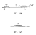
- FIG. 20A illustrates the pixel structure of the fourth embodiment after the third mask process
- FIG. 20B is a cross-sectional view taken along I line AA′ in FIG. 20A ;
- FIG. 20C is a cross-sectional view taken along line BB′ in FIG. 20A ;
- FIG. 21A illustrates the pixel structure of the fourth embodiment after the fourth mask process
- FIG. 21B is a cross-sectional view taken along line AA′ in FIG. 21A ;
- FIG. 21C is a cross-sectional view taken along line BB′ in FIG. 21A ;
- FIG. 22A illustrates the pixel structure of the fourth embodiment after the fifth mask process
- FIG. 22B is a cross-sectional view taken along line AA′ in FIG. 22A ;
- FIG. 22C is a cross-sectional view taken along line BB′ in FIG. 22A ;
- FIGS. 22D ⁇ 22I illustrate the detail steps of the fifth mask process of the fourth embodiment.
- FIG. 1 a flow chart of a method for manufacturing a pixel structure according to the first embodiment of the invention is illustrated.
- FIGS. 2A ⁇ 2C the pixel structure of the first embodiment after the first mask process and cross-sectional views taken along lines AA′ and BB′ in FIG. 2A are illustrated, respectively.
- a substrate 100 is provided.
- a patterned first metal layer 110 is formed on the substrate 100 by the first mask process.
- the patterned first metal layer 110 includes a gate electrode 112 , a first scan metal layer 114 and a first data metal segment 116 .
- the first scan metal layer 114 and the first data metal segment 116 surround a display area 101 and the first scan metal layer 114 has an interlacing region 12 , and the first data metal segment 116 and the interlacing region 12 are spaced at a first distance D 1 .
- the patterned first metal layer 110 further includes a patterned first metal layer 111 disposed on the substrate 100 .
- the patterned first metal layer 110 further includes a scan pad 118 and a data pad 119 disposed on the substrate 100 and electrically connected to the first scan metal layer 114 and the first data metal segment 116 , respectively.
- a patterned insulating layer 120 a patterned semi-conducting layer 130 and a patterned ohm contact layer 140 are formed by the second mask process.
- the step 13 can be performed by one photolithography process after an insulating material layer (not illustrated), a semi-conducting material layer (not illustrated) and an ohm contact material layer (not illustrated) are sequentially formed.
- the detail steps are stated as follows. First, the insulating material layer is deposited on the patterned first metal layer 110 .
- the semi-conducting material layer and the ohm contact material layer are sequentially deposited on the insulating material layer.
- a patterned photoresist layer (not illustrated) is formed on the ohm contact material layer and the semi-conducting material layer.
- the ohm contact material layer, the semi-conducting material layer and the insulating material layer are etched to form the patterned ohm contact layer 140 , the patterned semi-conducting layer 130 and the patterned insulating layer 120 .
- the patterned photoresist layer is removed.
- the patterned insulating layer 120 covers the gate electrode 112 , a part of the first data metal segment 116 and the first scan metal layer 114 .
- a patterned insulating layer 122 a patterned semi-conducting layer 132 , a patterned ohm contact layer 142 are formed as a separating layer 105 disposed across the first scan metal layer 114 in the interlacing region 12 .
- a patterned second metal layer 150 is formed by the third mask process.
- the patterned second metal layer 150 includes a source 153 , a drain 155 , a second scan metal layer 154 and a second data metal layer 156 .
- the first data metal segment 116 and the second data metal layer 156 constitute a data line 104 electrically connected to the source 153 .
- the first scan metal layer 114 and the second scan metal layer 154 constitute a scan line 102 electrically connected to the gate electrode 112 . Furthermore, the scan line 102 and the data line 104 are interlaced with each other in the interlacing region 12 .
- the data line 104 and the source 153 are coupled to each other.
- the data line 104 includes the first data metal segment 116 and the second data metal layer 156 .
- the second data metal layer 156 is disposed on the first data metal segment 116 and across the interlacing region 12 .
- the data line 104 further includes the separating layer 105 disposed across the scan line 102 .
- the second data metal layer 156 is disposed on the separating layer 105 . Therefore, the data line 104 is electrically isolated from the scan line 102 through the separating layer 105 so as to avoid a short circuit occurring.
- a patterned second metal layer 151 is formed on the patterned first metal layer 111 , and patterned second metal layers 157 , 159 are formed simultaneously in the step 14 to couple to the scan pad 118 and the data pad 119 , respectively.
- the patterned ohm contact layer 141 is etched to form a patterned ohm contact layer 141 a .
- the source 153 and the drain 155 are formed on a patterned semi-conducting layer 131 and the patterned ohm contact layer 141 a and constitute an active element 108 , such as a thin film transistor, with the gate electrode 112 .
- the patterned semi-conducting layer 131 and the patterned ohm contact layer 141 a constitute a channel layer 103 positioned on the patterned insulating layer 120 above the gate electrode 112 , as shown in FIG. 4B .
- FIGS. 5A ⁇ 5C the pixel structure of the first embodiment after the fourth mask process and cross-sectional views taken along lines AA′ and BB′ in FIG. 5A are illustrated, respectively. Then, as shown in the step 16 , a patterned passivation layer 160 a covering a part edge of the drain 155 is formed by the fourth mask process.
- a patterned transparent conductive layer 180 a is formed.
- the patterned transparent conductive layer 180 a includes a pixel electrode 182 a .
- patterned transparent conductive layers 187 a , 189 a of the patterned transparent conductive layer 180 a are coupled to the patterned second metal layers 157 , 159 , respectively.
- the pixel electrode 182 a is disposed across the patterned passivation layer 162 a on the part edge of the drain 155 to be electrically connected to the drain 155 . Therefore, the pixel electrode 182 a and the drain 155 have good electrical conduction because of the patterned passivation layer 162 a , and the situation for the pixel electrode 182 a to break during the formation can also be avoided.
- the material of the patterned transparent conductive layer 180 a is, for example, indium oxide (ITO).
- FIGS. 5D ⁇ 5I The steps 16 ⁇ 17 are elaborated in FIGS. 5D ⁇ 5I .
- FIGS. 5D ⁇ 5I the detail steps of the fourth mask process of the first embodiment are illustrated.
- a passivation material layer 160 is firstly formed.
- a patterned photoresist layer 170 is formed on the passivation material layer 160 .
- the patterned photoresist layer 170 includes a patterned photoresist layer 170 a with the thickness h 1 and a patterned photoresist layer 170 b with the thickness h 2 .
- the thickness h 1 is greater than the thickness h 2 .
- the step of forming the patterned photoresist layer 170 a can be performed by using a halftone mask or a gray-tone mask.
- the passivation material layer 160 is etched to form the patterned passivation layer 160 a .
- the patterned passivation layer 160 a includes a first passivation layer 161 a and the second passivation layer 162 a .
- the first passivation layer 161 a and the second passivation layer 162 a form a contact hole 165 to expose the drain 155 .
- the second passivation layer 162 a covers the part edge of the drain 155 .
- the patterned passivation layer 160 a includes a third passivation layer 163 a covering the patterned second metal layer 151 .
- the patterned photoresist layer 170 is ashed to expose the second passivation layer 162 a .
- the patterned photoresist layer 170 b is removed and the original patterned photoresist layer 170 a becomes a patterned photoresist layer 170 c with the thickness h 3 .
- a transparent conductive layer 180 is formed.
- the transparent conductive layer 180 is coupled to the drain 155 via the contact hole 165 .
- the remaining patterned photoresist layer 170 c is removed and part of the transparent conductive layer 180 on the remaining patterned photoresist layer 170 c is also removed so as to form the patterned transparent conductive layer 180 a .
- the transparent conductive layer 180 a includes the pixel electrode 182 a and a patterned transparent conductive layer 181 a covering the patterned second metal layer 151 .
- the pixel structure 10 is completed.
- the step of removing the remaining patterned photoresist layer 170 c includes the lift-off process.
- the patterned photoresist layer 170 c is removed by using chemicals or performing the laser lift-off process.
- the pixel structure 10 includes the active element 108 , the first passivation layer 161 a , the second passivation layer 162 a , the storage capacitor 106 and the pixel electrode 182 a .
- the active element 108 is closely adjacent to the interlacing region 12 and electrically coupled to the scan line 102 and the data line 104 .
- the active element 108 includes the gate electrode 112 , the patterned insulating layer 121 , the channel layer 103 , the source 153 and the drain 155 .
- the gate electrode 112 and the scan line 102 are electrically connected to each other.
- the patterned insulating layer 121 is positioned on the gate electrode 112 .
- the channel layer 103 is positioned on the patterned insulating layer 121 above the gate electrode 112 .
- the source 153 and the drain 155 are positioned on the channel layer 103 , and the source 153 is coupled to the data line 104 .
- the channel layer 103 includes the patterned ohm contact layer 141 a and the patterned semi-conducting layer 131 .
- the patterned ohm contact layer 141 a is disposed on the patterned semi-conducting layer 131 .
- the first passivation layer 161 a and the second passivation layer 162 a cover the active element 108 and form the contact hole 165 to expose the part of the drain 155 .
- the second passivation layer 162 a covers the part edge of the drain 155 .
- the storage capacitor 106 has a first capacitance metal layer 106 a and a second capacitance metal layer 106 b .
- the second capacitance metal layer 106 b is disposed on the first capacitance metal layer 106 a .
- the first capacitance metal layer 106 a includes the patterned first metal layer 111 and the patterned second metal layer 151 .
- the second capacitance metal layer 106 b includes the patterned transparent conductive layer 181 a .
- the patterned transparent conductive layer 181 a connected to the pixel electrode 182 a covers the third passivation layer 163 a .
- the third passivation layer 163 a disposed between the first capacitance metal layer 106 a and the second capacitance metal layer 106 b is used as a capacitance insulating layer. Therefore, in the embodiment, the storage capacitor 106 composed of a metal layer, an insulator and a transparent layer (such as ITO) is called MII capacitance structure.
- the method for manufacturing a pixel structure of the second embodiment differs from that of the first embodiment in using a halftone mask or a gray-tone mask in the second mask process. Therefore, an insulating layer and a semi-conducting layer of the pixel structure of the second embodiment are formed with different patterns, respectively.
- FIG. 6 a flow chart of a method for manufacturing a pixel structure according to the second embodiment of the invention is illustrated.
- FIGS. 7A ⁇ 7C the pixel structure of the second embodiment after the first mask process and cross-sectional views taken along lines AA′ and BB′ in FIG. 7A are illustrated, respectively.
- a substrate 100 is provided.
- a patterned first metal layer 110 is formed on the substrate 100 by the first mask process.
- the patterned first metal layer 110 includes a gate electrode 112 , a first scan metal layer 114 and a first data metal segment 116 .
- the first scan metal layer 114 and the first data metal segment 116 surround a display area 101 and the first scan metal layer 114 has an interlacing region 12 , and the first data metal segment 116 and the interlacing region 12 are spaced at a first distance D 1 .
- the patterned first metal layer 110 further includes a patterned first metal layer 111 disposed on the substrate 100 .
- the patterned first metal layer 110 further includes a scan pad 118 and a data pad 119 disposed on the substrate 100 and electrically connected to the first scan metal layer 114 and the first data metal segment 116 , respectively.
- the steps 21 , 22 and the steps 11 , 12 of the first embodiment are the same, respectively.
- a patterned insulating layer 220 a a patterned semi-conducting layer 230 b and a patterned ohm contact layer 240 b are formed by the second mask process.
- the step 23 differs from the step 13 of the first embodiment in using a halftone mask or a gray-tone mask to form a patterned photoresist layer with different thicknesses.
- the pattern of the patterned insulating layer 220 a is different from the patterns of the patterned semi-conducting layer 230 b and the patterned ohm contact layer 240 b .
- the patterned insulating layer 220 covers the display area 101 and exposes the first scan metal layer 114 , the first data metal segment 116 , the patterned first metal layer 111 , the scan pad 118 and the data pad 119 .
- a separating layer 205 disposed across the first scan metal layer 114 in the interlacing region 12 is formed.
- the separating layer 205 differs from the separating layer 105 of the first embodiment in the patterns.
- the patterns of the patterned ohm contact layer and the patterned semi-conducting layer in the separating layer 205 are different from the pattern of the patterned insulating layer.
- the step 23 is elaborated in FIGS. 8D ⁇ 8G .
- FIGS. 8D ⁇ 8G the detail steps of the second mask process of the second embodiment are illustrated.
- an insulating material layer 220 , a semi-conducting material layer 230 and an ohm contact material layer 240 are sequentially deposited on the patterned first metal layer 110 .
- a patterned photoresist layer 290 is formed on the semi-conducting material layer 230 .
- the patterned photoresist layer 290 includes a patterned photoresist layer 290 a with the thickness h 4 and a patterned photoresist layer 290 b with the thickness h 5 .
- the thickness h 4 is greater than the thickness h 5 .
- the ohm contact material layer 240 , the semi-conducting material layer 230 and the insulating material layer 220 are etched to form the patterned ohm contact layer 240 a , the patterned semi-conducting layer 230 a and the patterned insulating layer 220 a by using the patterned photoresist layer 290 as a mask.
- the pattered insulating layer 220 a exposes the first scan metal layer 114 , the first data metal segment 116 , the patterned first metal layer 111 , the scan pad 118 and the data pad 119 , as shown in FIG. 8A .
- the patterned photoresist layer 290 b with the thickness h 5 is ashed to expose a part of the patterned ohm contact layer 240 a and the patterned semi-conducting layer 230 a .
- the patterned photoresist layer 290 a with the thickness h 4 is cut off to form a patterned photoresist layer 290 c with the thickness h 6 .
- the exposed part of the patterned ohm contact layer 240 a and the patterned semi-conducting layer 230 a are etched to form the patterned ohm contact layer 240 b and the patterned semi-conducting layer 230 b .
- the patterned ohm contact layer 240 b and the patterned semi-conducting layer 230 b respectively include a patterned ohm contact layer 241 b and a patterned semi-conducting layer 231 b .
- the patterned ohm contact layer 241 b and patterned semi-conducting layer 231 b cover the patterned insulating layer 220 a on the gate electrode 121 .
- the remaining patterned photoresist layer 290 c is removed.
- a patterned second metal layer 250 is formed by the third mask process.
- the patterned second metal layer 250 includes a source 253 , and a drain 255 , a second scan metal layer 254 and a second data metal layer 256 .
- the first data metal segment 116 and the second data metal layer 256 constitute a data line 204 electrically connected to the source 253 .
- the first scan metal layer 114 and the second scan metal layer 254 constitute a scan line 202 electrically connected to the gate electrode 112 . Furthermore, the scan line 202 and the data line 204 are interlaced with each other in the interlacing region 12 .
- the second data metal layer 256 is disposed on the separating layer 205 and across the interlacing region 12 .
- a patterned second metal layer 251 is formed on the patterned first metal layer 111 , and patterned second metal layers 257 , 259 are formed to couple to the scan pad 118 and the data pad 119 in the step 24 at the same time.
- the patterned ohm contact layer 241 b is etched to become a patterned ohm contact layer 241 c .
- the source 253 and the drain 255 are formed on the patterned semi-conducting layer 231 b and the patterned ohm contact layer 241 c and constitute an active element 208 , such as a thin film transistor, with the gate electrode 112 .
- the patterned semi-conducting layer 231 b and the patterned ohm contact layer 241 c constitute a channel layer 203 , as shown in FIG. 9B .
- the data line 204 and the source 253 are coupled to each other.
- the data line 204 includes the first data metal segment 116 and the second data metal layer 256 .
- the second data metal layer 256 is disposed on the first data metal segment 116 .
- the data line 204 further includes the separating layer 205 disposed across the scan line 202 .
- the second data metal layer 256 is disposed on the separating layer 205 .
- a patterned passivation layer 260 a is formed by the fourth mask process.
- the patterned passivation layer 260 a partially covers a part edge of the drain 255 .
- a patterned transparent conductive layer 280 a including a pixel electrode 282 a is formed.
- the pixel electrode 282 a is disposed across the patterned passivation layer 262 a on the part edge of the drain 255 and electrically connected to the drain 255 .
- pattern transparent conductive layers 287 a , 289 a of the patterned transparent conductive layer 280 a are coupled to the patterned second metal layers 257 , 259 , respectively.
- the pixel electrode 282 a is disposed across the second passivation layer 262 a and coupled to the drain 255 via the contact hole 265 .
- FIGS. 10D ⁇ 10I The steps 26 ⁇ 27 are elaborated in FIGS. 10D ⁇ 10I .
- FIGS. 10D ⁇ 10I the detail steps of the fourth mask process of the second embodiment are illustrated.
- a passivation material layer 260 is firstly formed.
- a patterned photoresist layer 270 is formed on the passivation material layer 260 .
- the patterned photoresist layer 270 includes a patterned photoresist layer 270 a with the thickness h 1 and a patterned photoresist layer 270 b with the thickness h 2 .
- the thickness h 1 is greater than the thickness h 2 .
- the passivation material layer 260 is etched to form the patterned passivation layer 260 a .
- the patterned passivation layer 260 a includes a first passivation layer 261 a , a second passivation layer 262 a and a third passivation layer 263 a .
- the first passivation layer 261 a and the second passivation layer 262 a form the contact hole 265 to expose the drain 255 .
- the second passivation layer 262 a covers the part edge of the drain 255
- the third passivation layer 263 a covers the patterned second metal layer 251 .
- the patterned photoresist layer 270 is ashed to expose the second passivation layer 262 a .
- the patterned photoresist layer 270 b is removed. Therefore, the original patterned photoresist layer 270 a becomes a patterned photoresist layer 270 c with the thickness h 3 .
- a transparent conductive layer 280 is formed.
- the transparent conductive layer 280 is coupled to the drain 255 via the contact hole 265 .
- the remaining patterned photoresist layer 270 c is removed and part of the transparent conductive layer 280 on the remaining patterned photoresist layer 270 c is also removed concurrently so as to form the patterned transparent conductive layer 280 a .
- the patterned transparent conductive layer 280 a includes the pixel electrode 282 a and the patterned transparent conductive layer 281 a .
- the patterned transparent conductive layer 281 a covers the third passivation layer 263 a .
- the pixel structure 20 is completed.
- the step of removing the remaining patterned photoresist layer 270 c includes the lift-off process.
- the patterned photoresist layer 270 c is removed by using chemicals or performing the laser lift-off process.
- the pixel structure 20 includes the active element 208 , the first passivation layer 261 a , the second passivation layer 262 a , the third passivation layer 263 a , the storage capacitor 206 , the data line 202 and the pixel electrode 282 a .
- the active element 208 is closely adjacent to the interlacing region 12 and electrically coupled to the scan line 202 and the data line 204 .
- the active element 208 includes the gate electrode 112 , the patterned insulating layer 220 a , the channel layer 203 , the source 253 and the drain 255 .
- the gate electrode 112 and the scan line 202 are electrically connected to each other.
- the patterned insulating layer 220 a is positioned on the gate electrode 112 .
- the channel layer 203 is positioned on the patterned insulating layer 220 a above the gate electrode 112 .
- the source 253 and the drain 255 are positioned on the channel layer 203 , and the source 253 is coupled to the data line 204 .
- the channel layer 203 includes the patterned ohm contact layer 241 c and the patterned semi-conducting layer 231 b .
- the patterned ohm contact layer 241 c is disposed on the patterned semi-conducting layer 231 b.
- the first passivation layer 261 a and the second passivation layer 262 a cover the active element 208 and form the contact hole 265 to expose the part of the drain 255 .
- the second passivation layer 262 a covers the part edge of the drain 255 .
- the storage capacitor 206 has a first capacitance metal layer 206 a and a second capacitance metal layer 206 b .
- the second capacitance metal layer 206 b is disposed on the first capacitance metal layer 206 a .
- the first capacitance metal layer 260 a includes the patterned first metal layer 111 and the patterned second metal layer 251 .
- the second capacitance metal layer 206 b includes the patterned transparent conductive layer 281 a .
- a capacitance insulating layer includes the third passivation layer 263 a disposed between the first capacitance metal layer 206 a and the second capacitance metal layer 206 b . Therefore, in the embodiment, the storage capacitor 206 composed of a metal layer, an insulator and a transparent layer (such as ITO) is called MII capacitance structure.
- the method for manufacturing a pixel structure of the third embodiment differs from that of the first embodiment in using a halftone mask or a gray-tone mask in the second mask process. Therefore, an insulating layer and a semi-conducting layer of the pixel structure of the third embodiment are formed with different patterns, respectively. In addition, the patterns of a passivation layer and a transparent conductive layer are defined by the fourth mask process and the fifth mask process, respectively.
- FIG. 11 a flow chart of a method for manufacturing a pixel structure according to the third embodiment of the invention is illustrated.
- FIGS. 12A ⁇ 12C the pixel structure of the third embodiment after the first mask process and cross-sectional views taken along lines AA′ and BB′ in FIG. 12A are illustrated, respectively.
- a substrate 100 is provided.
- a patterned first metal layer 110 is formed on the substrate 100 by the first mask process.
- the patterned first metal layer 110 includes a gate electrode 112 , a first scan metal layer 114 and a first data metal segment 116 .
- the first scan metal layer 114 and the first data metal segment 116 surround a display area 101 and the first scan metal layer 114 has an interlacing region 12 , and the first data metal segment 116 and the interlacing region 12 are spaced at a first distance D 1 .
- the patterned first metal layer 110 further includes a patterned first metal layer 111 disposed on the substrate 100 .
- the patterned first metal layer 110 further includes a scan pad 118 and a data pad 119 disposed on the substrate 100 and electrically connected to the first scan metal layer 114 and the first data metal segment 116 , respectively.
- the steps 31 , 32 and the steps 11 , 12 of the first embodiment are the same, respectively.
- a patterned insulating layer 320 a a patterned semi-conducting layer 330 b and a patterned ohm contact layer 340 b are formed by the second mask process.
- the step 33 differs from the step 13 of the first embodiment in using a halftone mask or a gray-tone mask to form a patterned photoresist layer with different thicknesses.
- the pattern of the patterned insulating layer 320 a is different from the patterns of the patterned semi-conducting layer 330 b and the patterned ohm contact layer 340 b .
- the patterned insulating layer 320 a covers the display area 101 and exposes the first scan metal layer 114 , the first data metal segment 116 , the patterned first metal layer 111 , the scan pad 118 and the data pad 119 .
- a separating layer 305 disposed across the first scan metal layer 114 in the interlacing region 12 is formed.
- the step 33 is elaborated in FIGS. 13D ⁇ 13G .
- FIGS. 13D ⁇ 13G the detail steps of the second mask process of the third embodiment are illustrated.
- an insulating material layer 320 , a semi-conducting material layer 330 and an ohm contact material layer 340 are sequentially deposited on the patterned first metal layer 110 .
- a patterned photoresist layer 390 is formed on the semi-conducting material layer 330 .
- the patterned photoresist layer 390 includes a patterned photoresist layer 390 a with the thickness h 4 and a patterned photoresist layer 390 b with the thickness h 5 .
- the thickness h 4 is greater than the thickness h 5 .
- the ohm contact material layer 340 , the semi-conducting material layer 330 and the insulating material layer 320 are etched to form the patterned ohm contact layer 340 a , the patterned semi-conducting layer 330 a and the patterned insulating layer 320 a by using the patterned photoresist layer 390 as a mask.
- the pattered insulating layer 320 a exposes the first scan metal layer 114 , the first data metal segment 116 , the patterned first metal layer 111 , the scan pad 118 and the data pad 119 .
- the patterned photoresist layer 390 b with the thickness h 5 is ashed to expose the patterned ohm contact layer 340 a and the patterned semi-conducting layer 330 a .
- the patterned photoresist layer 390 a with the thickness h 4 is cut off to form a patterned photoresist layer 390 c with the thickness h 6 .
- the exposed part of the patterned ohm contact layer 340 a and the patterned semi-conducting layer 330 a are etched to form the patterned ohm contact layer 340 b and the patterned semi-conducting layer 330 b .
- the patterned ohm contact layer 340 b and the patterned semi-conducting layer 330 b respectively include a patterned ohm contact layer 341 b and a patterned semi-conducting layer 331 b positioned on the patterned insulating layer 320 a above the gate electrode 112 .
- the remaining patterned photoresist layer 390 c is removed.
- a patterned second metal layer 350 is formed by the third mask process.
- the patterned second metal layer 350 includes a source 353 , a drain 355 , a second scan metal layer 354 and a second data metal layer 356 .
- the first data metal segment 116 and the second data metal layer 356 constitute a data line 304 electrically connected to the source 353 .
- the first scan metal layer 114 and the second scan metal layer 354 constitute a scan line 302 electrically connected to the gate electrode 112 .
- Patterned second metal layers 357 , 359 are formed in the step 34 at the same time to couple to the scan pad 118 and the data pad 119 , respectively. Furthermore, the scan line 302 and the data line 304 are interlaced with each other in the interlacing region 12 .
- the second scan metal layer 354 includes several separate second scan metal segments 354 a , 354 b , 354 c .
- the second scan metal segments 354 a , 354 c are coupled to the first scan metal layer 114 exposed by the patterned insulating layer 320 a .
- the second scan metal segment 354 b is formed on the patterned insulating layer 320 a and electrically isolated from the first scan metal layer 114 .
- the data line 304 and the source 353 are coupled to each other.
- the data line 304 includes the first data metal segment 116 and the second data metal layer 356 .
- the second data metal layer 356 is disposed on the first data metal segment 116 and across the interlacing region 12 .
- the data line 304 further includes the separating layer 305 disposed across the scan line 302 .
- the second data metal layer 356 is disposed on the separating layer 305 .
- a patterned second metal layer 351 is formed in the step 34 at the same time.
- the patterned second metal layer 351 includes separate patterned second metal layers 351 a , 351 b , 351 c .
- the patterned second layers 351 a , 351 c are coupled to the patterned first metal layer 111 exposed by the patterned insulating layer 320 a .
- the patterned second metal layer 351 b is formed on the patterned insulating layer 320 a and electrically isolated from the patterned first metal layer 111 .
- the patterned ohm contact layer 341 b is etched to form a patterned ohm contact layer 341 c .
- the source 353 and the drain 355 are formed on the patterned semi-conducting layer 331 b and the patterned ohm contact layer 341 c and constitute an active element 308 , such as a thin film transistor, with the gate electrode 112 .
- the patterned semi-conducting layer 331 b and the patterned ohm contact layer 341 c constitute a channel layer 303 .
- a patterned passivation layer 360 is formed by the fourth mask process.
- the patterned passivation layer 360 includes a first passivation layer 361 and a second passivation layer 362 .
- the first passivation layer 361 and the second passivation layer 362 form a contact hole 365 to expose the drain 355 .
- the second passivation layer 362 covers a part edge of the drain 355 .
- the patterned passivation layer 360 further includes a third passivation layer 363 .
- the third passivation layer 363 covers the patterned second metal layer 351 b and forms a contact hole 367 to expose the patterned second metal layer 351 b .
- the invention is not limited thereto.
- the third passivation layer 363 can only cover an edge of the patterned second metal layer 351 b.
- the patterned passivation layer 360 also exposes the second scan metal segment 354 b and the patterned second metal layers 357 , 359 to couple to a transparent conductive layer formed later.
- a patterned transparent conductive layer 380 is formed by the fifth mask process.
- the patterned transparent conductive layer 380 includes a pixel electrode 382 .
- the pixel electrode 382 is disposed across the patterned passivation layer 362 on the part edge of the drain 355 to be electrically connected to the drain 355 .
- patterned transparent conductive layers 387 , 389 of the patterned transparent conductive layer 380 are coupled to the patterned second metal layers 357 , 359 , respectively.
- the patterned transparent conductive layer 380 further includes a patterned transparent conductive layer 381 and the patterned transparent conductive layers 387 , 389 .
- the patterned transparent conductive layers 381 , 387 , 389 are coupled to the patterned second metal layers 351 b , 357 , 359 , respectively.
- the pixel structure 30 is completed.
- the pixel structure 30 includes the active element 308 , the first passivation layer 361 , the second passivation layer 362 , the storage capacitor 306 , the data line 302 and the pixel electrode 382 .
- the active element 308 is closely adjacent to the interlacing region 12 and connected to the scan line 302 ad the data line 304 .
- the active element 308 includes the gate electrode 112 , the patterned insulating layer 320 a , the channel layer 303 , the source 353 and the drain 355 .
- the gate electrode 112 and the scan line 302 are electrically connected to each other.
- the patterned insulating layer 320 a is positioned on the gate electrode 112 .
- the channel layer 303 is positioned on the patterned insulating layer 320 a above the gate electrode 112 .
- the source 353 and the drain 355 are positioned on the channel layer 303 , and the source 353 is coupled to the data line 304 .
- the storage capacitor 306 has a first capacitance metal layer 306 a and a second capacitance metal layer 306 b .
- the second capacitance metal layer 306 b is disposed on the first capacitance metal layer 306 a .
- the first capacitance metal layer 306 a includes the patterned first metal layer 111
- the second capacitance metal layer 306 b includes the patterned second metal layer 351 b and the patterned transparent conductive layer 381 .
- a capacitance insulating layer includes a part of the patterned insulating layer 320 a disposed between the first capacitance metal layer 306 a and the second capacitance metal layer 306 b . Therefore, in the embodiment, the storage capacitor 306 composed of a metal layer, an insulator and a metal layer is called MIM capacitance structure.
- the method for manufacturing a pixel structure of the fourth embodiment differs from that of the first embodiment.
- the patterns of a semi-conducting layer and an insulating layer in the fourth embodiment are defined by the second mask process and the third mask process, respectively.
- the pattern of a second metal layer is defined by the fourth mask process.
- FIG. 17 a flow chart of a method for manufacturing a pixel structure according to the fourth embodiment of the invention is illustrated.
- FIGS. 18A ⁇ 18C the pixel structure of the fourth embodiment after the first mask process and cross-sectional views taken along lines AA′ and BB′ in FIG. 18A are illustrated, respectively.
- a substrate 100 is provided.
- a patterned first metal layer 110 is formed on the substrate 100 by the first mask process.
- the patterned first metal layer 110 includes a gate electrode 112 , a first scan metal layer 114 and a first data metal segment 116 .
- the first scan metal layer 114 and the first data metal segment 116 surround a display area 101 and the first scan metal layer 114 has an interlacing region 12 , and the first data metal segment 116 and the interlacing region 12 are spaced at a first distance D 1 .
- the patterned first metal layer 110 further includes a patterned first metal layer 111 disposed on the substrate 100 .
- the patterned first metal layer 110 further includes a scan pad 118 and a data pad 119 disposed on the substrate 100 and electrically connected to the first scan metal layer 114 and the first data metal segment 116 , respectively.
- the steps 41 , 42 and the steps 11 , 12 of the first embodiment are the same, respectively.
- FIGS. 19A ⁇ 19C the pixel structure of the fourth embodiment after the second mask process and cross-sectional views taken along lines AA′ and BB′ in FIG. 19A are illustrated, respectively.
- an insulating material layer 420 , a patterned semi-conducting layer 430 and a patterned ohm contact layer 440 are formed by the second mask process.
- the patterned semi-conducting layer 430 and the patterned ohm contact layer 440 are respectively positioned on a patterned semi-conducting layer 431 and a patterned ohm contact layer 441 above the gate electrode 112 .
- the step 43 differs from the step 13 of the first embodiment in only defining the patterns of the patterned semi-conducting layer 430 and the patterned ohm contact layer 440 . That is, only a semi-conducting material layer and an ohm contact material layer are etched.
- a separating layer 405 disposed across the first scan metal layer 114 is formed.
- the pixel structure of the fourth embodiment after the third mask process and cross-sectional views taken along lines AA′ and BB′ in FIG. 20A are illustrated, respectively.
- the insulating material layer 420 is patterned by the third mask process to form a patterned insulating layer 420 a .
- the patterned insulating layer 420 a exposes the first scan metal layer 114 , the first data metal segment 116 , the patterned first metal layer 111 , the scan pad 118 and the data pad 119 .
- a patterned second metal layer 450 is formed by the fourth mask process.
- the patterned second metal layer 450 includes a source 453 , a drain 455 , a second scan metal layer 454 and a second data metal layer 456 .
- the first data metal segment 116 and the second scan metal layer 456 constitute a data line 404 electrically connected to the source 453 .
- the first scan metal layer 114 and the second scan metal layer 454 constitute a scan line 402 electrically connected to the gate electrode 112 .
- the scan line 402 and the data line 404 are interlaced with each other in the interlacing region 12 .
- Patterned second metal layers 457 , 459 are formed to respectively couple the scan pad 118 and the data pad 119 in the step 45 at the same time.
- the second scan metal layer 454 includes several separate second scan metal segments 454 a , 454 b , 454 c .
- the second scan metal segments 454 a , 454 c are coupled to the first scan metal layer 114 exposed by the patterned insulating layer 420 a .
- the second scan metal segment 454 b is formed on the patterned insulating layer 420 a to electrically isolate from the first scan metal layer 114 .
- the scan line 404 further includes the separating layer 405 disposed across the scan line 402 .
- the second data metal layer 456 is disposed on the separating layer 405 and across the interlacing region 12 .
- a patterned second metal layer 451 is formed in the step 45 at the same time.
- the patterned second metal layer 451 includes separate patterned second metal layers 451 a , 451 b , 451 c .
- the patterned second metal layers 451 a , 451 c are coupled to the patterned first metal layer 111 exposed by the patterned insulating layer 420 a .
- the patterned second metal layer 451 b is formed on the patterned insulating layer 420 a to electrically isolate from the patterned first metal layer 111 .
- the patterned ohm contact layer 441 is etched to form an ohm contact layer 441 a .
- the source 453 and the drain 455 are formed on the patterned semi-conducting layer 431 and the ohm contact layer 441 a and constitute an active element 408 , such as a thin film transistor, with the gate electrode 112 .
- the patterned semi-conducting layer 431 and the ohm contact layer 441 a constitute a channel layer 403 .
- a patterned passivation layer 460 a is formed by the fifth mask process.
- the patterned passivation layer 460 a partially covers a part edge of the drain 455 .
- a patterned transparent conductive layer 480 a is formed.
- the patterned transparent conductive layer 480 a includes a pixel electrode 482 a .
- the pixel electrode 482 a is disposed across a patterned passivation layer 462 a on the part edge of the drain 455 and electrically connected to the drain 455 .
- patterned transparent conductive layers 487 a , 489 a of the patterned transparent conductive layer 480 a are coupled to the patterned second metal layers 457 , 459 , respectively.
- the steps 47 ⁇ 48 are elaborated in FIGS. 22D ⁇ 22I .
- FIGS. 22D ⁇ 22I the detail steps of the fifth mask process of the fourth embodiment are illustrated.
- a passivation material layer 460 is firstly formed.
- a patterned photoresist layer 470 is formed on the passivation material layer 460 .
- the patterned photoresist layer 470 includes a patterned photoresist layer 470 a with the thickness h 1 and a patterned photoresist layer 470 b with the thickness h 2 .
- the thickness h 1 is greater than the thickness h 2 .
- the passivation material layer 460 is etched to form the patterned passivation layer 460 a .
- the patterned passivation layer 460 a includes a first passivation layer 461 a , a second passivation layer 462 a and a third passivation layer 463 a .
- the first passivation layer 461 a and the second passivation layer 462 a form a contact hole 465 to expose the drain 455
- the second passivation layer 462 a covers the part edge of the drain 455 .
- the third passivation layer 463 a forms a contact hole 467 to expose the patterned second metal layer 451 b .
- the invention is not limited thereto.
- the third passivation layer 463 a can only cover a part edge of the patterned second metal layer 451 b.
- the patterned photoresist layer 470 is ashed to expose the second passivation layer 462 a and the third passivation layer 463 a .
- the patterned photoresist layer 470 b is removed.
- the original patterned photoresist layer 470 a becomes a patterned photoresist layer 470 c with the thickness h 3 .
- a transparent conductive layer 480 is formed.
- the transparent conductive layer 480 is coupled to the drain 455 and the patterned second metal layer 451 b via the contact hole 465 .
- the remaining patterned photoresist layer 470 c is removed and part of the transparent conductive layer 480 on the remaining patterned photoresist layer 470 c is also removed concurrently so as to form the patterned transparent conductive layer 480 a .
- the patterned transparent conductive layer 480 a includes the pixel electrode 482 a and a patterned transparent conductive layer 481 a coupled to the patterned second metal layer 451 b .
- the pixel structure 40 is completed.
- the step of removing the remaining patterned photoresist layer 470 c includes the lift-off process.
- the patterned photoresist layer 470 c is removed by using chemicals or performing the laser lift-off process.
- the pixel structure 40 includes the active element 408 , the first passivation layer 461 a , the second passivation layer 462 a , the storage capacitor 406 , the data line 402 and the pixel electrode 482 .
- the active element 408 is closely adjacent to the interlacing region 12 and electrically connected to the scan line 402 and the data line 404 .
- the active element 408 includes the gate electrode 112 , the patterned insulating layer 420 a , the channel layer 403 , the source 453 and the drain 455 .
- the gate electrode 112 and the scan line 402 are electrically connected to each other.
- the patterned insulating layer 420 a is positioned on the gate electrode 112 .
- the channel layer 403 is positioned on the patterned insulating layer 420 a above the gate electrode 112 .
- the source 453 and the drain 455 are positioned on the channel layer 403 , and the source 453 is coupled to the data line 404 .
- the channel layer 403 includes the ohm contact layer 441 a and the patterned semi-conducting layer 431 .
- the ohm contact layer 441 a is disposed on the patterned semi-conducting layer 431 .
- the first passivation layer 461 a and the second passivation layer 462 a cover the active element 408 and form the contact hole 465 to expose the part of the drain 455 .
- the second passivation layer 462 a covers the part edge of the drain 455 .
- the storage capacitor 406 has a first capacitance metal layer 406 a and a second capacitance metal layer 406 b .
- the second capacitance metal layer 406 b is disposed on the first capacitance metal layer 406 a .
- the first capacitance metal layer 406 a includes the first patterned metal layer 111
- the second capacitance metal layer 406 b includes the second patterned metal layer 451 b and the patterned transparent conductive layer 481 a .
- a capacitance insulating layer includes a part of the patterned insulating layer 420 a disposed between the first capacitance metal layer 406 a and the second capacitance metal layer 406 b . Therefore, in the embodiment, the storage capacitor 406 composed of a metal layer, an insulator and a metal layer is called MIM capacitance structure.
- the manufacturing cost of the pixel structure is greatly decreased by using only four masks or five masks.
- the scan line and data line of the pixel structure of each embodiment are double-metal structures, so that the transmission resistance values of the signal lines (the scan line and the data line) are remarkably reduced to avoid the signals decaying and delaying.
- the passivation layer of the pixel structure is formed on the edge of the drain in each embodiment, and the transparent conductive layer is disposed across the passivation layer to contact the drain. Therefore, the drain and the pixel electrode have good electrical conduction, and the situation for the pixel electrode to break during the formation can be avoided.
Abstract
A pixel structure includes a scan line, a data line, an active element, a first passivation layer, a second passivation layer and a pixel electrode. The data line includes a first data metal segment and a second data metal layer. The active element includes a gate electrode, an insulating layer, a channel layer, a source and a drain. The channel layer is positioned on the insulating layer above the gate electrode. The source and the drain are positioned on the channel layer. The source is coupled to the data line. The first passivation layer and the second passivation layer cover the active element and form a first contact hole to expose a part of the drain. The second passivation layer covers a part edge of the drain. The pixel electrode is disposed across the second passivation layer and coupled to the drain via the first contact hole.
Description
This application is a Divisional of and claims the priority benefit of U.S. patent application Ser. No. 12/081,515, filed Apr. 17, 2008, now pending, which claims the priority benefits of Taiwan application Serial No. 97103007, filed Jan. 25, 2008. The entirety of each of the above-mentioned patent applications is hereby incorporated by reference herein and made a part of this specification.
1. Field of the Invention
The invention relates in general to a pixel structure and a method for manufacturing the same, and more particularly to a pixel structure having multi-metal signal lines and a method for manufacturing the same.
2. Description of the Related Art
In most of the traditional flat display device technology, several thin film transistors are cooperated with a pixel array formed by several signal lines. The thin film transistors of each pixel in the pixel array are controlled by control signals from the signal lines to selectively receive data according to the pulse of the control signals.
However, as the size of the flat display device increases, the resistance values of the signal lines increase accordingly. In addition, due to the increase of the overlapping area of the signal lines, the RC delay of the signals occurs more frequently to cause the signal transmission distortion.
Thus, how to decease the resistance values of the signal lines so as to avoid the signal distortion is critical for the quality of the large size flat display device.
The invention is directed to a pixel structure and a method for manufacturing the same. The pixel structure has double-metal signal lines, so that the transmission resistance values of the signal lines is reduced to provide a flat display device with the stable and precise signal transmission quality. In addition, the number of the mask processes of the method for manufacturing the pixel structure is reduced to remarkably decrease the manufacturing cost.
According to the invention, a pixel structure including a scan line, a data line, an active element, a first passivation layer, a second passivation layer and a pixel electrode is provided. The scan line has a first scan metal layer and a second scan metal layer. The data line is interlaced with the scan line to form an interlacing region. The data line includes a first data metal segment and a second data metal layer. The first data metal segment and the interlacing region are spaced at a first distance. The second data metal layer is disposed on the first data metal segment and across the interlacing region. The active element electrically coupled to the scan line and the data line includes a gate electrode, an insulating layer, a channel layer, a drain and a source. The gate electrode is electrically connected to the scan line. The insulating layer is partially positioned on the gate electrode. The channel layer is positioned on the insulating layer above the gate electrode. The source and the drain are positioned on the channel layer. The source is coupled to the data line. The first passivation layer and the second passivation layer cover the active element and form a first contact hole to expose a part of the drain. The second passivation layer covers a part edge of the drain. The pixel electrode is disposed across the second passivation layer and is coupled to the drain via the first contact hole.
According to the invention, a method for manufacturing a pixel structure includes following steps is provided. First, a substrate is provided. Then, a patterned first metal layer is formed on the substrate. The patterned first metal layer includes a gate electrode, a first scan metal layer and a first data metal segment. After that, a patterned insulating layer is formed on the patterned first metal layer. Then, a patterned semi-conducting layer is formed on the patterned insulating layer. After that, a patterned second metal layer including a source, a drain, a second scan metal layer and a second data metal layer is formed. The source and the drain are formed on the patterned semi-conducting layer and constitute an active element with the gate electrode. The first data metal segment and the second data metal layer constitute a data line electrically connected to the source. The first scan metal layer and the second scan metal layer constitute a scan line electrically connected to the gate electrode. Then, a patterned passivation layer partially covering a part edge of the drain is formed. After that, a patterned transparent conductive layer including a pixel electrode is formed. The pixel electrode is disposed across the patterned passivation layer on the part edge of the drain and electrically connected to the drain.
Other objects, features, and advantages of the invention will become apparent from the following detailed description of the preferred but non-limiting embodiments. The following description is made with reference to the accompanying drawings.
First Embodiment
Referring to FIG. 1 , a flow chart of a method for manufacturing a pixel structure according to the first embodiment of the invention is illustrated. Referring to FIGS. 2A˜2C at the same time, the pixel structure of the first embodiment after the first mask process and cross-sectional views taken along lines AA′ and BB′ in FIG. 2A are illustrated, respectively.
Please refer to FIG. 2A . First, as shown in the step 11, a substrate 100 is provided. Then, as shown in the step 12, a patterned first metal layer 110 is formed on the substrate 100 by the first mask process. The patterned first metal layer 110 includes a gate electrode 112, a first scan metal layer 114 and a first data metal segment 116. The first scan metal layer 114 and the first data metal segment 116 surround a display area 101 and the first scan metal layer 114 has an interlacing region 12, and the first data metal segment 116 and the interlacing region 12 are spaced at a first distance D1. In addition, as shown in FIG. 2B , the patterned first metal layer 110 further includes a patterned first metal layer 111 disposed on the substrate 100. Besides, as shown in FIG. 2A and FIG. 2C , the patterned first metal layer 110 further includes a scan pad 118 and a data pad 119 disposed on the substrate 100 and electrically connected to the first scan metal layer 114 and the first data metal segment 116, respectively.
Referring to FIGS. 3A˜3C at the same time, the pixel structure of the first embodiment after the second mask process and cross-sectional views taken along lines AA′ and BB′ in FIG. 3A are illustrated, respectively. After that, as shown in the step 13, a patterned insulating layer 120, a patterned semi-conducting layer 130 and a patterned ohm contact layer 140 are formed by the second mask process. The step 13 can be performed by one photolithography process after an insulating material layer (not illustrated), a semi-conducting material layer (not illustrated) and an ohm contact material layer (not illustrated) are sequentially formed. The detail steps are stated as follows. First, the insulating material layer is deposited on the patterned first metal layer 110. Then, the semi-conducting material layer and the ohm contact material layer are sequentially deposited on the insulating material layer. After that, a patterned photoresist layer (not illustrated) is formed on the ohm contact material layer and the semi-conducting material layer. Then, the ohm contact material layer, the semi-conducting material layer and the insulating material layer are etched to form the patterned ohm contact layer 140, the patterned semi-conducting layer 130 and the patterned insulating layer 120. After that, the patterned photoresist layer is removed. The patterned insulating layer 120 covers the gate electrode 112, a part of the first data metal segment 116 and the first scan metal layer 114.
Besides, as shown in FIG. 3A and FIG. 3C , a patterned insulating layer 122, a patterned semi-conducting layer 132, a patterned ohm contact layer 142 are formed as a separating layer 105 disposed across the first scan metal layer 114 in the interlacing region 12.
Referring to FIGS. 4A˜4C at the same time, the pixel structure of the first embodiment after the third mask process and cross-sectional views taken along lines AA′ and BB′ in FIG. 4A are illustrated, respectively. Then, as shown in the step 14, a patterned second metal layer 150 is formed by the third mask process. The patterned second metal layer 150 includes a source 153, a drain 155, a second scan metal layer 154 and a second data metal layer 156. The first data metal segment 116 and the second data metal layer 156 constitute a data line 104 electrically connected to the source 153. The first scan metal layer 114 and the second scan metal layer 154 constitute a scan line 102 electrically connected to the gate electrode 112. Furthermore, the scan line 102 and the data line 104 are interlaced with each other in the interlacing region 12.
As shown in FIGS. 4A˜4C , the data line 104 and the source 153 are coupled to each other. The data line 104 includes the first data metal segment 116 and the second data metal layer 156. The second data metal layer 156 is disposed on the first data metal segment 116 and across the interlacing region 12.
In addition, as shown in FIG. 4A and FIG. 4C , the data line 104 further includes the separating layer 105 disposed across the scan line 102. The second data metal layer 156 is disposed on the separating layer 105. Therefore, the data line 104 is electrically isolated from the scan line 102 through the separating layer 105 so as to avoid a short circuit occurring.
Besides, a patterned second metal layer 151 is formed on the patterned first metal layer 111, and patterned second metal layers 157, 159 are formed simultaneously in the step 14 to couple to the scan pad 118 and the data pad 119, respectively.
After that, as shown in the step 15, the patterned ohm contact layer 141 is etched to form a patterned ohm contact layer 141 a. The source 153 and the drain 155 are formed on a patterned semi-conducting layer 131 and the patterned ohm contact layer 141 a and constitute an active element 108, such as a thin film transistor, with the gate electrode 112. The patterned semi-conducting layer 131 and the patterned ohm contact layer 141 a constitute a channel layer 103 positioned on the patterned insulating layer 120 above the gate electrode 112, as shown in FIG. 4B .
Referring to FIGS. 5A˜5C at the same time, the pixel structure of the first embodiment after the fourth mask process and cross-sectional views taken along lines AA′ and BB′ in FIG. 5A are illustrated, respectively. Then, as shown in the step 16, a patterned passivation layer 160 a covering a part edge of the drain 155 is formed by the fourth mask process.
After that, as shown in the step 17, a patterned transparent conductive layer 180 a is formed. The patterned transparent conductive layer 180 a includes a pixel electrode 182 a. Besides, patterned transparent conductive layers 187 a, 189 a of the patterned transparent conductive layer 180 a are coupled to the patterned second metal layers 157, 159, respectively.
In the embodiment, the pixel electrode 182 a is disposed across the patterned passivation layer 162 a on the part edge of the drain 155 to be electrically connected to the drain 155. Therefore, the pixel electrode 182 a and the drain 155 have good electrical conduction because of the patterned passivation layer 162 a, and the situation for the pixel electrode 182 a to break during the formation can also be avoided. Preferably, the material of the patterned transparent conductive layer 180 a is, for example, indium oxide (ITO).
The steps 16˜17 are elaborated in FIGS. 5D˜5I . Referring to FIGS. 5D˜5I , the detail steps of the fourth mask process of the first embodiment are illustrated. As shown in FIG. 5D , a passivation material layer 160 is firstly formed.
Then, as shown in FIG. 5E , a patterned photoresist layer 170 is formed on the passivation material layer 160. The patterned photoresist layer 170 includes a patterned photoresist layer 170 a with the thickness h1 and a patterned photoresist layer 170 b with the thickness h2. The thickness h1 is greater than the thickness h2. The step of forming the patterned photoresist layer 170 a can be performed by using a halftone mask or a gray-tone mask.
After that, as shown in FIG. 5F , the passivation material layer 160 is etched to form the patterned passivation layer 160 a. The patterned passivation layer 160 a includes a first passivation layer 161 a and the second passivation layer 162 a. The first passivation layer 161 a and the second passivation layer 162 a form a contact hole 165 to expose the drain 155. The second passivation layer 162 a covers the part edge of the drain 155.
Besides, the patterned passivation layer 160 a includes a third passivation layer 163 a covering the patterned second metal layer 151.
Then, as shown in FIG. 5G , the patterned photoresist layer 170 is ashed to expose the second passivation layer 162 a. After the patterned photoresist layer 170 is ashed, the patterned photoresist layer 170 b is removed and the original patterned photoresist layer 170 a becomes a patterned photoresist layer 170 c with the thickness h3.
After that, as shown in FIG. 5H , a transparent conductive layer 180 is formed. The transparent conductive layer 180 is coupled to the drain 155 via the contact hole 165.
Then, as shown in FIG. 5I , the remaining patterned photoresist layer 170 c is removed and part of the transparent conductive layer 180 on the remaining patterned photoresist layer 170 c is also removed so as to form the patterned transparent conductive layer 180 a. The transparent conductive layer 180 a includes the pixel electrode 182 a and a patterned transparent conductive layer 181 a covering the patterned second metal layer 151. Heretofore, the pixel structure 10 is completed. The step of removing the remaining patterned photoresist layer 170 c includes the lift-off process. Preferably, the patterned photoresist layer 170 c is removed by using chemicals or performing the laser lift-off process.
As shown in FIG. 5A and FIG. 5B , the pixel structure 10 includes the active element 108, the first passivation layer 161 a, the second passivation layer 162 a, the storage capacitor 106 and the pixel electrode 182 a. The active element 108 is closely adjacent to the interlacing region 12 and electrically coupled to the scan line 102 and the data line 104. The active element 108 includes the gate electrode 112, the patterned insulating layer 121, the channel layer 103, the source 153 and the drain 155. The gate electrode 112 and the scan line 102 are electrically connected to each other. The patterned insulating layer 121 is positioned on the gate electrode 112. The channel layer 103 is positioned on the patterned insulating layer 121 above the gate electrode 112. The source 153 and the drain 155 are positioned on the channel layer 103, and the source 153 is coupled to the data line 104. The channel layer 103 includes the patterned ohm contact layer 141 a and the patterned semi-conducting layer 131. The patterned ohm contact layer 141 a is disposed on the patterned semi-conducting layer 131.
As shown in FIG. 5B , the first passivation layer 161 a and the second passivation layer 162 a cover the active element 108 and form the contact hole 165 to expose the part of the drain 155. The second passivation layer 162 a covers the part edge of the drain 155.
As shown in FIG. 5B , the storage capacitor 106 has a first capacitance metal layer 106 a and a second capacitance metal layer 106 b. The second capacitance metal layer 106 b is disposed on the first capacitance metal layer 106 a. The first capacitance metal layer 106 a includes the patterned first metal layer 111 and the patterned second metal layer 151. The second capacitance metal layer 106 b includes the patterned transparent conductive layer 181 a. The patterned transparent conductive layer 181 a connected to the pixel electrode 182 a covers the third passivation layer 163 a. The third passivation layer 163 a disposed between the first capacitance metal layer 106 a and the second capacitance metal layer 106 b is used as a capacitance insulating layer. Therefore, in the embodiment, the storage capacitor 106 composed of a metal layer, an insulator and a transparent layer (such as ITO) is called MII capacitance structure.
Second Embodiment
The method for manufacturing a pixel structure of the second embodiment differs from that of the first embodiment in using a halftone mask or a gray-tone mask in the second mask process. Therefore, an insulating layer and a semi-conducting layer of the pixel structure of the second embodiment are formed with different patterns, respectively.
Referring to FIG. 6 , a flow chart of a method for manufacturing a pixel structure according to the second embodiment of the invention is illustrated. Referring to FIGS. 7A˜7C at the same time, the pixel structure of the second embodiment after the first mask process and cross-sectional views taken along lines AA′ and BB′ in FIG. 7A are illustrated, respectively.
Please refer to FIG. 7A . First, as shown in the step 21, a substrate 100 is provided. Then, as shown in the step 22, a patterned first metal layer 110 is formed on the substrate 100 by the first mask process. The patterned first metal layer 110 includes a gate electrode 112, a first scan metal layer 114 and a first data metal segment 116. The first scan metal layer 114 and the first data metal segment 116 surround a display area 101 and the first scan metal layer 114 has an interlacing region 12, and the first data metal segment 116 and the interlacing region 12 are spaced at a first distance D1. In addition, as shown in FIG. 7B , the patterned first metal layer 110 further includes a patterned first metal layer 111 disposed on the substrate 100. Besides, as shown in FIG. 7C , the patterned first metal layer 110 further includes a scan pad 118 and a data pad 119 disposed on the substrate 100 and electrically connected to the first scan metal layer 114 and the first data metal segment 116, respectively. Basically, the steps 21, 22 and the steps 11, 12 of the first embodiment are the same, respectively.
Referring to FIGS. 8A˜8C at the same time, the pixel structure of the second embodiment after the second mask process and cross-sectional views taken along lines AA′ and BB′ in FIG. 8A are illustrated, respectively. Then, as shown in the step 23, a patterned insulating layer 220 a, a patterned semi-conducting layer 230 b and a patterned ohm contact layer 240 b are formed by the second mask process. The step 23 differs from the step 13 of the first embodiment in using a halftone mask or a gray-tone mask to form a patterned photoresist layer with different thicknesses. Therefore, the pattern of the patterned insulating layer 220 a is different from the patterns of the patterned semi-conducting layer 230 b and the patterned ohm contact layer 240 b. Besides, the patterned insulating layer 220 covers the display area 101 and exposes the first scan metal layer 114, the first data metal segment 116, the patterned first metal layer 111, the scan pad 118 and the data pad 119.
In addition, as shown in FIG. 8A , a separating layer 205 disposed across the first scan metal layer 114 in the interlacing region 12 is formed. The separating layer 205 differs from the separating layer 105 of the first embodiment in the patterns. The patterns of the patterned ohm contact layer and the patterned semi-conducting layer in the separating layer 205 are different from the pattern of the patterned insulating layer.
The step 23 is elaborated in FIGS. 8D˜8G . Referring to FIGS. 8D˜8G , the detail steps of the second mask process of the second embodiment are illustrated. As shown in FIG. 8D , an insulating material layer 220, a semi-conducting material layer 230 and an ohm contact material layer 240 are sequentially deposited on the patterned first metal layer 110. Then, a patterned photoresist layer 290 is formed on the semi-conducting material layer 230. The patterned photoresist layer 290 includes a patterned photoresist layer 290 a with the thickness h4 and a patterned photoresist layer 290 b with the thickness h5. The thickness h4 is greater than the thickness h5.
After that, as shown in FIG. 8E , the ohm contact material layer 240, the semi-conducting material layer 230 and the insulating material layer 220 are etched to form the patterned ohm contact layer 240 a, the patterned semi-conducting layer 230 a and the patterned insulating layer 220 a by using the patterned photoresist layer 290 as a mask. The pattered insulating layer 220 a exposes the first scan metal layer 114, the first data metal segment 116, the patterned first metal layer 111, the scan pad 118 and the data pad 119, as shown in FIG. 8A .
Then, as shown in FIG. 8F , the patterned photoresist layer 290 b with the thickness h5 is ashed to expose a part of the patterned ohm contact layer 240 a and the patterned semi-conducting layer 230 a. The patterned photoresist layer 290 a with the thickness h4 is cut off to form a patterned photoresist layer 290 c with the thickness h6.
After that, as shown in FIG. 8G , the exposed part of the patterned ohm contact layer 240 a and the patterned semi-conducting layer 230 a are etched to form the patterned ohm contact layer 240 b and the patterned semi-conducting layer 230 b. The patterned ohm contact layer 240 b and the patterned semi-conducting layer 230 b respectively include a patterned ohm contact layer 241 b and a patterned semi-conducting layer 231 b. The patterned ohm contact layer 241 b and patterned semi-conducting layer 231 b cover the patterned insulating layer 220 a on the gate electrode 121. Then, the remaining patterned photoresist layer 290 c is removed.
Referring to FIGS. 9A˜9C at the same time, the pixel structure of the second embodiment after the third mask process and cross-sectional views taken along lines AA′ and BB′ in FIG. 9A are illustrated, respectively. As shown in the step 24, a patterned second metal layer 250 is formed by the third mask process. The patterned second metal layer 250 includes a source 253, and a drain 255, a second scan metal layer 254 and a second data metal layer 256. The first data metal segment 116 and the second data metal layer 256 constitute a data line 204 electrically connected to the source 253. The first scan metal layer 114 and the second scan metal layer 254 constitute a scan line 202 electrically connected to the gate electrode 112. Furthermore, the scan line 202 and the data line 204 are interlaced with each other in the interlacing region 12.
Besides, as shown in FIG. 9A and FIG. 9C , the second data metal layer 256 is disposed on the separating layer 205 and across the interlacing region 12.
In addition, a patterned second metal layer 251 is formed on the patterned first metal layer 111, and patterned second metal layers 257, 259 are formed to couple to the scan pad 118 and the data pad 119 in the step 24 at the same time.
Then, as shown in the step 25, the patterned ohm contact layer 241 b is etched to become a patterned ohm contact layer 241 c. The source 253 and the drain 255 are formed on the patterned semi-conducting layer 231 b and the patterned ohm contact layer 241 c and constitute an active element 208, such as a thin film transistor, with the gate electrode 112. The patterned semi-conducting layer 231 b and the patterned ohm contact layer 241 c constitute a channel layer 203, as shown in FIG. 9B .
As shown in FIGS. 9A˜9C , the data line 204 and the source 253 are coupled to each other. The data line 204 includes the first data metal segment 116 and the second data metal layer 256. The second data metal layer 256 is disposed on the first data metal segment 116. The data line 204 further includes the separating layer 205 disposed across the scan line 202. The second data metal layer 256 is disposed on the separating layer 205.
Referring to FIGS. 10A˜10C at the same time, the pixel structure of the second embodiment after the fourth mask process and cross-sectional views taken along lines AA′ and BB′ in FIG. 10A are illustrated, respectively. As shown in the step 26, a patterned passivation layer 260 a is formed by the fourth mask process. The patterned passivation layer 260 a partially covers a part edge of the drain 255.
After that, as shown in the step 27, a patterned transparent conductive layer 280 a including a pixel electrode 282 a is formed. The pixel electrode 282 a is disposed across the patterned passivation layer 262 a on the part edge of the drain 255 and electrically connected to the drain 255. In addition, pattern transparent conductive layers 287 a, 289 a of the patterned transparent conductive layer 280 a are coupled to the patterned second metal layers 257, 259, respectively.
As shown in FIG. 10B , the pixel electrode 282 a is disposed across the second passivation layer 262 a and coupled to the drain 255 via the contact hole 265.
The steps 26˜27 are elaborated in FIGS. 10D˜10I . Referring to FIGS. 10D˜10I , the detail steps of the fourth mask process of the second embodiment are illustrated. As shown in FIG. 10D , a passivation material layer 260 is firstly formed.
Then, as shown in FIG. 10E , a patterned photoresist layer 270 is formed on the passivation material layer 260. The patterned photoresist layer 270 includes a patterned photoresist layer 270 a with the thickness h1 and a patterned photoresist layer 270 b with the thickness h2. The thickness h1 is greater than the thickness h2.
After that, as shown in FIG. 10F , the passivation material layer 260 is etched to form the patterned passivation layer 260 a. The patterned passivation layer 260 a includes a first passivation layer 261 a, a second passivation layer 262 a and a third passivation layer 263 a. The first passivation layer 261 a and the second passivation layer 262 a form the contact hole 265 to expose the drain 255. The second passivation layer 262 a covers the part edge of the drain 255, and the third passivation layer 263 a covers the patterned second metal layer 251.
Then, as shown in FIG. 10G , the patterned photoresist layer 270 is ashed to expose the second passivation layer 262 a. After the patterned photoresist layer 270 is ashed, the patterned photoresist layer 270 b is removed. Therefore, the original patterned photoresist layer 270 a becomes a patterned photoresist layer 270 c with the thickness h3.
After that, as shown in FIG. 10H , a transparent conductive layer 280 is formed. The transparent conductive layer 280 is coupled to the drain 255 via the contact hole 265.
Then, as shown in FIG. 10I , the remaining patterned photoresist layer 270 c is removed and part of the transparent conductive layer 280 on the remaining patterned photoresist layer 270 c is also removed concurrently so as to form the patterned transparent conductive layer 280 a. The patterned transparent conductive layer 280 a includes the pixel electrode 282 a and the patterned transparent conductive layer 281 a. The patterned transparent conductive layer 281 a covers the third passivation layer 263 a. Heretofore, the pixel structure 20 is completed. The step of removing the remaining patterned photoresist layer 270 c includes the lift-off process. Preferably, the patterned photoresist layer 270 c is removed by using chemicals or performing the laser lift-off process.
As shown in FIG. 10A and FIG. 10B , the pixel structure 20 includes the active element 208, the first passivation layer 261 a, the second passivation layer 262 a, the third passivation layer 263 a, the storage capacitor 206, the data line 202 and the pixel electrode 282 a. The active element 208 is closely adjacent to the interlacing region 12 and electrically coupled to the scan line 202 and the data line 204. The active element 208 includes the gate electrode 112, the patterned insulating layer 220 a, the channel layer 203, the source 253 and the drain 255. The gate electrode 112 and the scan line 202 are electrically connected to each other. The patterned insulating layer 220 a is positioned on the gate electrode 112. The channel layer 203 is positioned on the patterned insulating layer 220 a above the gate electrode 112. The source 253 and the drain 255 are positioned on the channel layer 203, and the source 253 is coupled to the data line 204. The channel layer 203 includes the patterned ohm contact layer 241 c and the patterned semi-conducting layer 231 b. The patterned ohm contact layer 241 c is disposed on the patterned semi-conducting layer 231 b.
As shown in FIG. 10I , the first passivation layer 261 a and the second passivation layer 262 a cover the active element 208 and form the contact hole 265 to expose the part of the drain 255. The second passivation layer 262 a covers the part edge of the drain 255.
As shown in FIG. 10I , the storage capacitor 206 has a first capacitance metal layer 206 a and a second capacitance metal layer 206 b. The second capacitance metal layer 206 b is disposed on the first capacitance metal layer 206 a. The first capacitance metal layer 260 a includes the patterned first metal layer 111 and the patterned second metal layer 251. The second capacitance metal layer 206 b includes the patterned transparent conductive layer 281 a. A capacitance insulating layer includes the third passivation layer 263 a disposed between the first capacitance metal layer 206 a and the second capacitance metal layer 206 b. Therefore, in the embodiment, the storage capacitor 206 composed of a metal layer, an insulator and a transparent layer (such as ITO) is called MII capacitance structure.
Third Embodiment
The method for manufacturing a pixel structure of the third embodiment differs from that of the first embodiment in using a halftone mask or a gray-tone mask in the second mask process. Therefore, an insulating layer and a semi-conducting layer of the pixel structure of the third embodiment are formed with different patterns, respectively. In addition, the patterns of a passivation layer and a transparent conductive layer are defined by the fourth mask process and the fifth mask process, respectively.
Referring to FIG. 11 , a flow chart of a method for manufacturing a pixel structure according to the third embodiment of the invention is illustrated. Referring to FIGS. 12A˜12C at the same time, the pixel structure of the third embodiment after the first mask process and cross-sectional views taken along lines AA′ and BB′ in FIG. 12A are illustrated, respectively.
Please refer to FIG. 12A . First, as shown in the step 31, a substrate 100 is provided. Then, as shown in the step 32, a patterned first metal layer 110 is formed on the substrate 100 by the first mask process. The patterned first metal layer 110 includes a gate electrode 112, a first scan metal layer 114 and a first data metal segment 116. The first scan metal layer 114 and the first data metal segment 116 surround a display area 101 and the first scan metal layer 114 has an interlacing region 12, and the first data metal segment 116 and the interlacing region 12 are spaced at a first distance D1. In addition, as shown in FIG. 12B , the patterned first metal layer 110 further includes a patterned first metal layer 111 disposed on the substrate 100. In addition, as shown in FIG. 12C , the patterned first metal layer 110 further includes a scan pad 118 and a data pad 119 disposed on the substrate 100 and electrically connected to the first scan metal layer 114 and the first data metal segment 116, respectively. Basically, the steps 31, 32 and the steps 11, 12 of the first embodiment are the same, respectively.
Referring to FIGS. 13A˜13C at the same time, the pixel structure of the third embodiment after the second mask process and cross-sectional views taken along lines AA′ and BB′ in FIG. 13A are illustrated, respectively. Then, as shown in the step 33, a patterned insulating layer 320 a, a patterned semi-conducting layer 330 b and a patterned ohm contact layer 340 b are formed by the second mask process. The step 33 differs from the step 13 of the first embodiment in using a halftone mask or a gray-tone mask to form a patterned photoresist layer with different thicknesses. Therefore, the pattern of the patterned insulating layer 320 a is different from the patterns of the patterned semi-conducting layer 330 b and the patterned ohm contact layer 340 b. Besides, the patterned insulating layer 320 a covers the display area 101 and exposes the first scan metal layer 114, the first data metal segment 116, the patterned first metal layer 111, the scan pad 118 and the data pad 119.
Besides, as shown in FIG. 13A , a separating layer 305 disposed across the first scan metal layer 114 in the interlacing region 12 is formed.
The step 33 is elaborated in FIGS. 13D˜13G . Referring to FIGS. 13D˜13G , the detail steps of the second mask process of the third embodiment are illustrated. As shown in FIG. 13D , an insulating material layer 320, a semi-conducting material layer 330 and an ohm contact material layer 340 are sequentially deposited on the patterned first metal layer 110. Then, a patterned photoresist layer 390 is formed on the semi-conducting material layer 330. The patterned photoresist layer 390 includes a patterned photoresist layer 390 a with the thickness h4 and a patterned photoresist layer 390 b with the thickness h5. The thickness h4 is greater than the thickness h5.
After that, as shown in FIG. 13E , the ohm contact material layer 340, the semi-conducting material layer 330 and the insulating material layer 320 are etched to form the patterned ohm contact layer 340 a, the patterned semi-conducting layer 330 a and the patterned insulating layer 320 a by using the patterned photoresist layer 390 as a mask. The pattered insulating layer 320 a exposes the first scan metal layer 114, the first data metal segment 116, the patterned first metal layer 111, the scan pad 118 and the data pad 119.
Then, as shown in FIG. 13F , the patterned photoresist layer 390 b with the thickness h5 is ashed to expose the patterned ohm contact layer 340 a and the patterned semi-conducting layer 330 a. The patterned photoresist layer 390 a with the thickness h4 is cut off to form a patterned photoresist layer 390 c with the thickness h6.
After that, as shown in FIG. 13G , the exposed part of the patterned ohm contact layer 340 a and the patterned semi-conducting layer 330 a are etched to form the patterned ohm contact layer 340 b and the patterned semi-conducting layer 330 b. The patterned ohm contact layer 340 b and the patterned semi-conducting layer 330 b respectively include a patterned ohm contact layer 341 b and a patterned semi-conducting layer 331 b positioned on the patterned insulating layer 320 a above the gate electrode 112. Then, the remaining patterned photoresist layer 390 c is removed.
Referring to FIGS. 14A˜14C at the same time, the pixel structure of the third embodiment after the third mask process and cross-sectional views taken along lines AA′ and BB′ in FIG. 14A are illustrated, respectively. As shown in the step 34, a patterned second metal layer 350 is formed by the third mask process. The patterned second metal layer 350 includes a source 353, a drain 355, a second scan metal layer 354 and a second data metal layer 356. The first data metal segment 116 and the second data metal layer 356 constitute a data line 304 electrically connected to the source 353. The first scan metal layer 114 and the second scan metal layer 354 constitute a scan line 302 electrically connected to the gate electrode 112. Patterned second metal layers 357, 359 are formed in the step 34 at the same time to couple to the scan pad 118 and the data pad 119, respectively. Furthermore, the scan line 302 and the data line 304 are interlaced with each other in the interlacing region 12.
As shown in FIG. 14A , the second scan metal layer 354 includes several separate second scan metal segments 354 a, 354 b, 354 c. The second scan metal segments 354 a, 354 c are coupled to the first scan metal layer 114 exposed by the patterned insulating layer 320 a. The second scan metal segment 354 b is formed on the patterned insulating layer 320 a and electrically isolated from the first scan metal layer 114.
Besides, as shown in FIG. 14A , the data line 304 and the source 353 are coupled to each other. The data line 304 includes the first data metal segment 116 and the second data metal layer 356. The second data metal layer 356 is disposed on the first data metal segment 116 and across the interlacing region 12. The data line 304 further includes the separating layer 305 disposed across the scan line 302. The second data metal layer 356 is disposed on the separating layer 305.
In addition, as shown in FIG. 14A , a patterned second metal layer 351 is formed in the step 34 at the same time. The patterned second metal layer 351 includes separate patterned second metal layers 351 a, 351 b, 351 c. The patterned second layers 351 a, 351 c are coupled to the patterned first metal layer 111 exposed by the patterned insulating layer 320 a. The patterned second metal layer 351 b is formed on the patterned insulating layer 320 a and electrically isolated from the patterned first metal layer 111.
Then, as shown in the step 35, the patterned ohm contact layer 341 b is etched to form a patterned ohm contact layer 341 c. The source 353 and the drain 355 are formed on the patterned semi-conducting layer 331 b and the patterned ohm contact layer 341 c and constitute an active element 308, such as a thin film transistor, with the gate electrode 112. The patterned semi-conducting layer 331 b and the patterned ohm contact layer 341 c constitute a channel layer 303.
Referring to FIGS. 15A˜15C at the same time, the pixel structure of the third embodiment after the fourth mask process and cross-sectional views taken along lines AA′ and BB′ in FIG. 15A are illustrated, respectively. As shown in the step 36, a patterned passivation layer 360 is formed by the fourth mask process. The patterned passivation layer 360 includes a first passivation layer 361 and a second passivation layer 362. The first passivation layer 361 and the second passivation layer 362 form a contact hole 365 to expose the drain 355. The second passivation layer 362 covers a part edge of the drain 355.
In addition, the patterned passivation layer 360 further includes a third passivation layer 363. The third passivation layer 363 covers the patterned second metal layer 351 b and forms a contact hole 367 to expose the patterned second metal layer 351 b. However, the invention is not limited thereto. The third passivation layer 363 can only cover an edge of the patterned second metal layer 351 b.
Besides, the patterned passivation layer 360 also exposes the second scan metal segment 354 b and the patterned second metal layers 357, 359 to couple to a transparent conductive layer formed later.
Referring to FIGS. 16A˜16C at the same time, the pixel structure of the third embodiment after the fifth mask process and cross-sectional views taken along lines AA′ and BB′ in FIG. 16A are illustrated, respectively. As shown in the step 37, a patterned transparent conductive layer 380 is formed by the fifth mask process. The patterned transparent conductive layer 380 includes a pixel electrode 382. The pixel electrode 382 is disposed across the patterned passivation layer 362 on the part edge of the drain 355 to be electrically connected to the drain 355. In addition, patterned transparent conductive layers 387, 389 of the patterned transparent conductive layer 380 are coupled to the patterned second metal layers 357, 359, respectively.
Besides, the patterned transparent conductive layer 380 further includes a patterned transparent conductive layer 381 and the patterned transparent conductive layers 387, 389. The patterned transparent conductive layers 381, 387, 389 are coupled to the patterned second metal layers 351 b, 357, 359, respectively. Heretofore, the pixel structure 30 is completed.
As shown in FIG. 16A and FIG. 16B , the pixel structure 30 includes the active element 308, the first passivation layer 361, the second passivation layer 362, the storage capacitor 306, the data line 302 and the pixel electrode 382. The active element 308 is closely adjacent to the interlacing region 12 and connected to the scan line 302 ad the data line 304. The active element 308 includes the gate electrode 112, the patterned insulating layer 320 a, the channel layer 303, the source 353 and the drain 355. The gate electrode 112 and the scan line 302 are electrically connected to each other. The patterned insulating layer 320 a is positioned on the gate electrode 112. The channel layer 303 is positioned on the patterned insulating layer 320 a above the gate electrode 112. The source 353 and the drain 355 are positioned on the channel layer 303, and the source 353 is coupled to the data line 304.
As shown in FIG. 16B , the storage capacitor 306 has a first capacitance metal layer 306 a and a second capacitance metal layer 306 b. The second capacitance metal layer 306 b is disposed on the first capacitance metal layer 306 a. The first capacitance metal layer 306 a includes the patterned first metal layer 111, and the second capacitance metal layer 306 b includes the patterned second metal layer 351 b and the patterned transparent conductive layer 381. A capacitance insulating layer includes a part of the patterned insulating layer 320 a disposed between the first capacitance metal layer 306 a and the second capacitance metal layer 306 b. Therefore, in the embodiment, the storage capacitor 306 composed of a metal layer, an insulator and a metal layer is called MIM capacitance structure.
Fourth Embodiment
The method for manufacturing a pixel structure of the fourth embodiment differs from that of the first embodiment. The patterns of a semi-conducting layer and an insulating layer in the fourth embodiment are defined by the second mask process and the third mask process, respectively. The pattern of a second metal layer is defined by the fourth mask process.
Referring to FIG. 17 , a flow chart of a method for manufacturing a pixel structure according to the fourth embodiment of the invention is illustrated. Referring to FIGS. 18A˜18C at the same time, the pixel structure of the fourth embodiment after the first mask process and cross-sectional views taken along lines AA′ and BB′ in FIG. 18A are illustrated, respectively.
Please refer to FIG. 18A . First, as shown in the step 41, a substrate 100 is provided. Then, as shown in the step 42, a patterned first metal layer 110 is formed on the substrate 100 by the first mask process. The patterned first metal layer 110 includes a gate electrode 112, a first scan metal layer 114 and a first data metal segment 116. The first scan metal layer 114 and the first data metal segment 116 surround a display area 101 and the first scan metal layer 114 has an interlacing region 12, and the first data metal segment 116 and the interlacing region 12 are spaced at a first distance D1. In addition, as shown in FIG. 18B , the patterned first metal layer 110 further includes a patterned first metal layer 111 disposed on the substrate 100. As shown in FIG. 18C , the patterned first metal layer 110 further includes a scan pad 118 and a data pad 119 disposed on the substrate 100 and electrically connected to the first scan metal layer 114 and the first data metal segment 116, respectively. Basically, the steps 41, 42 and the steps 11, 12 of the first embodiment are the same, respectively.
Referring to FIGS. 19A˜19C at the same time, the pixel structure of the fourth embodiment after the second mask process and cross-sectional views taken along lines AA′ and BB′ in FIG. 19A are illustrated, respectively. As shown in the step 43, an insulating material layer 420, a patterned semi-conducting layer 430 and a patterned ohm contact layer 440 are formed by the second mask process. The patterned semi-conducting layer 430 and the patterned ohm contact layer 440 are respectively positioned on a patterned semi-conducting layer 431 and a patterned ohm contact layer 441 above the gate electrode 112. The step 43 differs from the step 13 of the first embodiment in only defining the patterns of the patterned semi-conducting layer 430 and the patterned ohm contact layer 440. That is, only a semi-conducting material layer and an ohm contact material layer are etched.
Besides, as shown in FIG. 19A , a separating layer 405 disposed across the first scan metal layer 114 is formed.
Referring to FIGS. 20A˜20C at the same time, the pixel structure of the fourth embodiment after the third mask process and cross-sectional views taken along lines AA′ and BB′ in FIG. 20A are illustrated, respectively. As shown in the step 44, the insulating material layer 420 is patterned by the third mask process to form a patterned insulating layer 420 a. The patterned insulating layer 420 a exposes the first scan metal layer 114, the first data metal segment 116, the patterned first metal layer 111, the scan pad 118 and the data pad 119.
Referring to FIGS. 21A˜21C at the same time, the pixel structure of the fourth embodiment after the fourth mask process and cross-sectional views taken along lines AA′ and BB′ in FIG. 21A are illustrated, respectively. As shown in the step 45, a patterned second metal layer 450 is formed by the fourth mask process. The patterned second metal layer 450 includes a source 453, a drain 455, a second scan metal layer 454 and a second data metal layer 456. The first data metal segment 116 and the second scan metal layer 456 constitute a data line 404 electrically connected to the source 453. The first scan metal layer 114 and the second scan metal layer 454 constitute a scan line 402 electrically connected to the gate electrode 112. Furthermore, the scan line 402 and the data line 404 are interlaced with each other in the interlacing region 12. Patterned second metal layers 457, 459 are formed to respectively couple the scan pad 118 and the data pad 119 in the step 45 at the same time.
As shown in FIG. 21A , the second scan metal layer 454 includes several separate second scan metal segments 454 a, 454 b, 454 c. The second scan metal segments 454 a, 454 c are coupled to the first scan metal layer 114 exposed by the patterned insulating layer 420 a. The second scan metal segment 454 b is formed on the patterned insulating layer 420 a to electrically isolate from the first scan metal layer 114.
In addition, as shown in FIG. 21A , the scan line 404 further includes the separating layer 405 disposed across the scan line 402. The second data metal layer 456 is disposed on the separating layer 405 and across the interlacing region 12.
Besides, as shown in FIG. 21A , a patterned second metal layer 451 is formed in the step 45 at the same time. The patterned second metal layer 451 includes separate patterned second metal layers 451 a, 451 b, 451 c. The patterned second metal layers 451 a, 451 c are coupled to the patterned first metal layer 111 exposed by the patterned insulating layer 420 a. The patterned second metal layer 451 b is formed on the patterned insulating layer 420 a to electrically isolate from the patterned first metal layer 111.
Then, as shown in the step 46, the patterned ohm contact layer 441 is etched to form an ohm contact layer 441 a. The source 453 and the drain 455 are formed on the patterned semi-conducting layer 431 and the ohm contact layer 441 a and constitute an active element 408, such as a thin film transistor, with the gate electrode 112. The patterned semi-conducting layer 431 and the ohm contact layer 441 a constitute a channel layer 403.
Referring to FIGS. 22A˜22C at the same time, the pixel structure of the fourth embodiment after the fifth mask process and cross-sectional views taken along lines AA′ and BB′ in FIG. 22A are illustrated, respectively. As shown in the step 47, a patterned passivation layer 460 a is formed by the fifth mask process. The patterned passivation layer 460 a partially covers a part edge of the drain 455.
After that, as shown in the step 48, a patterned transparent conductive layer 480 a is formed. The patterned transparent conductive layer 480 a includes a pixel electrode 482 a. The pixel electrode 482 a is disposed across a patterned passivation layer 462 a on the part edge of the drain 455 and electrically connected to the drain 455. In addition, patterned transparent conductive layers 487 a, 489 a of the patterned transparent conductive layer 480 a are coupled to the patterned second metal layers 457, 459, respectively.
The steps 47˜48 are elaborated in FIGS. 22D˜22I . Referring to FIGS. 22D˜22I , the detail steps of the fifth mask process of the fourth embodiment are illustrated. As shown in FIG. 22D , a passivation material layer 460 is firstly formed.
Then, as shown in FIG. 22E , a patterned photoresist layer 470 is formed on the passivation material layer 460. The patterned photoresist layer 470 includes a patterned photoresist layer 470 a with the thickness h1 and a patterned photoresist layer 470 b with the thickness h2. The thickness h1 is greater than the thickness h2.
After that, as shown in FIG. 22F , the passivation material layer 460 is etched to form the patterned passivation layer 460 a. The patterned passivation layer 460 a includes a first passivation layer 461 a, a second passivation layer 462 a and a third passivation layer 463 a. The first passivation layer 461 a and the second passivation layer 462 a form a contact hole 465 to expose the drain 455, and the second passivation layer 462 a covers the part edge of the drain 455. The third passivation layer 463 a forms a contact hole 467 to expose the patterned second metal layer 451 b. However, the invention is not limited thereto. The third passivation layer 463 a can only cover a part edge of the patterned second metal layer 451 b.
Then, as shown in FIG. 22G , the patterned photoresist layer 470 is ashed to expose the second passivation layer 462 a and the third passivation layer 463 a. After the patterned photoresist layer 470 is ashed, the patterned photoresist layer 470 b is removed. The original patterned photoresist layer 470 a becomes a patterned photoresist layer 470 c with the thickness h3.
After that, as shown in FIG. 22H , a transparent conductive layer 480 is formed. The transparent conductive layer 480 is coupled to the drain 455 and the patterned second metal layer 451 b via the contact hole 465.
Then, as shown in FIG. 22I , the remaining patterned photoresist layer 470 c is removed and part of the transparent conductive layer 480 on the remaining patterned photoresist layer 470 c is also removed concurrently so as to form the patterned transparent conductive layer 480 a. The patterned transparent conductive layer 480 a includes the pixel electrode 482 a and a patterned transparent conductive layer 481 a coupled to the patterned second metal layer 451 b. Heretofore, the pixel structure 40 is completed. The step of removing the remaining patterned photoresist layer 470 c includes the lift-off process. Preferably, the patterned photoresist layer 470 c is removed by using chemicals or performing the laser lift-off process.
As shown in FIG. 22A and FIG. 22B , the pixel structure 40 includes the active element 408, the first passivation layer 461 a, the second passivation layer 462 a, the storage capacitor 406, the data line 402 and the pixel electrode 482. The active element 408 is closely adjacent to the interlacing region 12 and electrically connected to the scan line 402 and the data line 404. The active element 408 includes the gate electrode 112, the patterned insulating layer 420 a, the channel layer 403, the source 453 and the drain 455. The gate electrode 112 and the scan line 402 are electrically connected to each other. The patterned insulating layer 420 a is positioned on the gate electrode 112. The channel layer 403 is positioned on the patterned insulating layer 420 a above the gate electrode 112. The source 453 and the drain 455 are positioned on the channel layer 403, and the source 453 is coupled to the data line 404. The channel layer 403 includes the ohm contact layer 441 a and the patterned semi-conducting layer 431. The ohm contact layer 441 a is disposed on the patterned semi-conducting layer 431.
As shown in FIG. 22B , the first passivation layer 461 a and the second passivation layer 462 a cover the active element 408 and form the contact hole 465 to expose the part of the drain 455. The second passivation layer 462 a covers the part edge of the drain 455.
As shown in FIG. 22B , the storage capacitor 406 has a first capacitance metal layer 406 a and a second capacitance metal layer 406 b. The second capacitance metal layer 406 b is disposed on the first capacitance metal layer 406 a. The first capacitance metal layer 406 a includes the first patterned metal layer 111, and the second capacitance metal layer 406 b includes the second patterned metal layer 451 b and the patterned transparent conductive layer 481 a. A capacitance insulating layer includes a part of the patterned insulating layer 420 a disposed between the first capacitance metal layer 406 a and the second capacitance metal layer 406 b. Therefore, in the embodiment, the storage capacitor 406 composed of a metal layer, an insulator and a metal layer is called MIM capacitance structure.
According to the pixel structure and the method for manufacturing the same disclosed in the above embodiments of the invention, the manufacturing cost of the pixel structure is greatly decreased by using only four masks or five masks. Besides, the scan line and data line of the pixel structure of each embodiment are double-metal structures, so that the transmission resistance values of the signal lines (the scan line and the data line) are remarkably reduced to avoid the signals decaying and delaying. In addition, the passivation layer of the pixel structure is formed on the edge of the drain in each embodiment, and the transparent conductive layer is disposed across the passivation layer to contact the drain. Therefore, the drain and the pixel electrode have good electrical conduction, and the situation for the pixel electrode to break during the formation can be avoided.
While the invention has been described by way of example and in terms of a preferred embodiment, it is to be understood that the invention is not limited thereto. On the contrary, it is intended to cover various modifications and similar arrangements and procedures, and the scope of the appended claims therefore should be accorded the broadest interpretation so as to encompass all such modifications and similar arrangements and procedures.
Claims (30)
1. A pixel structure, comprising:
a scan line having a first scan metal layer and a second scan metal layer;
a data line interlaced with the scan line to form an interlacing region, wherein the data line comprises a first data metal segment and a second data metal layer, the first data metal segment and the interlacing region are spaced at a first distance, and the second data metal layer is disposed on the first data metal segment and across the interlacing region;
an active element electrically coupled to the scan line and the data line, comprising:
a gate electrode electrically connected to the scan line;
an insulating layer partially formed on the gate electrode;
a channel layer formed on the insulating layer above the gate electrode; and
a source and a drain formed on the channel layer, wherein the source is coupled to the data line;
a first passivation layer and a second passivation layer covering the active element, wherein a first contact hole exposing a region of the drain is formed between the first passivation layer and the second passivation layer, the first passivation layer and the second passivation layer cover sidewalls of the drain, and the region of the drain exposed by the first contact hole is not connected with the sidewalls of the drain ; and
a pixel electrode disposed across the second passivation layer and coupled to the drain via the first contact hole.
2. The pixel structure according to claim 1 , wherein the channel layer comprises an ohm contact layer and a semi-conducting layer, and the ohm contact layer is disposed on the semi-conducting layer.
3. The pixel structure according to claim 1 , further comprising a storage capacitor having a first capacitance metal layer and a second capacitance metal layer, wherein the second capacitance metal layer is disposed above the first capacitance metal layer.
4. The pixel structure according to claim 3 , further comprising a third passivation layer partially covering an edge of the second capacitance metal layer.
5. The pixel structure according to claim 4 , wherein the pixel electrode covers the third passivation layer.
6. The pixel structure according to claim 3 , wherein the storage capacitor further has a capacitance insulating layer disposed between the first capacitance metal layer and the second capacitance metal layer.
7. The pixel structure according to claim 6 , further comprising a third passivation layer covering an edge of the second capacitance metal layer.
8. The pixel structure according to claim 7 , wherein the third passivation layer has a second contact hole, and the pixel electrode is coupled to the second capacitance metal layer via the second contact hole.
9. The pixel structure according to claim 1 , wherein the data line further comprises a separating layer disposed across the scan line, and the second data metal layer is disposed on the separating layer.
10. The pixel structure according to claim 1 , wherein the second scan metal layer comprises a plurality of second scan metal segments.
11. The pixel structure according to claim 1 , further comprising a plurality of scan pads, and the scan pads being electrically connected to the first scan metal layer.
12. The pixel structure according to claim 11 , further comprising a patterned metal layer, and the patterned metal layer coupling to the scan pads respectively.
13. The pixel structure according to claim 12 , further comprising a patterned transparent conductive layer, and the patterned transparent conductive layer coupling to the patterned metal layer.
14. The pixel structure according to claim 13 , wherein the patterned transparent conductive layer is an indium oxide layer.
15. The pixel structure according to claim 13 , wherein a material of the patterned transparent conductive layer is the same as that of the pixel electrode.
16. The pixel structure according to claim 1 , further comprising a plurality of data pads, and the data pads being electrically connected to the first data metal segment.
17. The pixel structure according to claim 16 , further comprising a patterned metal layer, and the patterned metal layer coupling to the data pads respectively.
18. The pixel structure according to claim 17 , further comprising a patterned transparent conductive layer, and the patterned transparent conductive layer coupling to the patterned metal layer.
19. The pixel structure according to claim 18 , wherein the patterned transparent conductive layer is an indium oxide layer.
20. The pixel structure according to claim 18 , wherein a material of the patterned transparent conductive layer is the same as that of the pixel electrode.
21. A pixel structure, comprising:
a scan line having a first scan metal layer and a second scan metal layer;
a data line interlaced with the scan line to form an interlacing region, wherein the data line comprises a first data metal segment and a second data metal layer, the first data metal segment and the interlacing region are spaced at a first distance, the second data metal layer is disposed on the first data metal segment and across the interlacing region, and the second scan metal layer is stacked on the first scan metal layer and directly contacts with the first scan metal layer;
an active element electrically coupled to the scan line and the data line, comprising:
a gate electrode electrically connected to the scan line;
an insulating layer partially formed on the gate electrode;
a channel layer formed on the insulating layer above the gate electrode; and
a source and a drain formed on the channel layer, wherein the source is coupled to the data line;
a first passivation layer and a second passivation layer covering the active element and forming a first contact hole to expose a part of the drain, wherein the second passivation layer covers a part edge of the drain; and
a pixel electrode disposed across the second passivation layer and coupled to the drain via the first contact hole.
22. The pixel structure according to claim 21 , wherein the channel layer comprises an ohm contact layer and a semi-conducting layer, and the ohm contact layer is disposed on the semi-conducting layer.
23. The pixel structure according to claim 21 , further comprising:
a storage capacitor having a first capacitance metal layer and a second capacitance metal layer, wherein the second capacitance metal layer is disposed above the first capacitance metal layer; and
a third passivation layer partially covering an edge of the second capacitance metal layer, and the pixel electrode covering the third passivation layer.
24. The pixel structure according to claim 21 , further comprising:
a storage capacitor having a first capacitance metal layer and a second capacitance metal layer, wherein the second capacitance metal layer is disposed above the first capacitance metal layer, and the storage capacitor further has a capacitance insulating layer disposed between the first capacitance metal layer and the second capacitance metal layer; and
a third passivation layer covering an edge of the second capacitance metal layer, wherein the third passivation layer has a second contact hole, and the pixel electrode is coupled to the second capacitance metal layer via the second contact hole.
25. The pixel structure according to claim 21 , wherein the data line further comprises a separating layer disposed across the scan line, and the second data metal layer is disposed on the separating layer.
26. The pixel structure according to claim 21 , wherein the second scan metal layer comprises a plurality of second scan metal segments.
27. The pixel structure according to claim 21 , further comprising:
a plurality of scan pads, the scan pads being electrically connected to the first scan metal layer;
a patterned metal layer, the patterned metal layer coupling to the scan pads respectively; and
a patterned transparent conductive layer, the patterned transparent conductive layer coupling to the patterned metal layer, wherein the patterned transparent conductive layer is an indium oxide layer.
28. The pixel structure according to claim 27 , wherein a material of the patterned transparent conductive layer is the same as that of the pixel electrode.
29. The pixel structure according to claim 21 , further comprising:
a plurality of data pads, the data pads being electrically connected to the first data metal segment;
a patterned metal layer, the patterned metal layer coupling to the data pads respectively; and
a patterned transparent conductive layer, the patterned transparent conductive layer coupling to the patterned metal layer, wherein the patterned transparent conductive layer is an indium oxide layer.
30. The pixel structure according to claim 29 , wherein a material of the patterned transparent conductive layer is the same as that of the pixel electrode.
Priority Applications (1)
| Application Number | Priority Date | Filing Date | Title |
|---|---|---|---|
| US13/163,780 US8426894B2 (en) | 2008-01-25 | 2011-06-20 | Pixel structure |
Applications Claiming Priority (5)
| Application Number | Priority Date | Filing Date | Title |
|---|---|---|---|
| TW97103007 | 2008-01-25 | ||
| TW097103007A TWI371640B (en) | 2008-01-25 | 2008-01-25 | Pixel structure and method for manufacturing the same |
| TW97103007A | 2008-01-25 | ||
| US12/081,515 US20090191652A1 (en) | 2008-01-25 | 2008-04-17 | Pixel structure and method for manufacturing the same |
| US13/163,780 US8426894B2 (en) | 2008-01-25 | 2011-06-20 | Pixel structure |
Related Parent Applications (1)
| Application Number | Title | Priority Date | Filing Date |
|---|---|---|---|
| US12/081,515 Division US20090191652A1 (en) | 2008-01-25 | 2008-04-17 | Pixel structure and method for manufacturing the same |
Publications (2)
| Publication Number | Publication Date |
|---|---|
| US20110241009A1 US20110241009A1 (en) | 2011-10-06 |
| US8426894B2 true US8426894B2 (en) | 2013-04-23 |
Family
ID=40899647
Family Applications (3)
| Application Number | Title | Priority Date | Filing Date |
|---|---|---|---|
| US12/081,515 Abandoned US20090191652A1 (en) | 2008-01-25 | 2008-04-17 | Pixel structure and method for manufacturing the same |
| US13/163,774 Active 2028-05-25 US8420463B2 (en) | 2008-01-25 | 2011-06-20 | Method for manufacturing pixel structure |
| US13/163,780 Active 2028-05-31 US8426894B2 (en) | 2008-01-25 | 2011-06-20 | Pixel structure |
Family Applications Before (2)
| Application Number | Title | Priority Date | Filing Date |
|---|---|---|---|
| US12/081,515 Abandoned US20090191652A1 (en) | 2008-01-25 | 2008-04-17 | Pixel structure and method for manufacturing the same |
| US13/163,774 Active 2028-05-25 US8420463B2 (en) | 2008-01-25 | 2011-06-20 | Method for manufacturing pixel structure |
Country Status (2)
| Country | Link |
|---|---|
| US (3) | US20090191652A1 (en) |
| TW (1) | TWI371640B (en) |
Families Citing this family (6)
| Publication number | Priority date | Publication date | Assignee | Title |
|---|---|---|---|---|
| KR20050089381A (en) * | 2004-03-04 | 2005-09-08 | 삼성에스디아이 주식회사 | Fabrication method of active matrix type display device |
| TWI423195B (en) * | 2010-10-18 | 2014-01-11 | Au Optronics Corp | Pixel structure |
| CN102097051B (en) * | 2010-11-03 | 2012-10-31 | 友达光电股份有限公司 | Pixel structure |
| TWI615664B (en) * | 2013-11-08 | 2018-02-21 | 友達光電股份有限公司 | Pixel array |
| US10971530B2 (en) * | 2018-04-20 | 2021-04-06 | Wuhan China Star Optoelectronics Technology Co., Ltd. | Manufacturing method for a TFT array substrate and TFT array substrate |
| CN112185248A (en) * | 2019-07-05 | 2021-01-05 | 瀚宇彩晶股份有限公司 | Pixel structure |
Citations (9)
| Publication number | Priority date | Publication date | Assignee | Title |
|---|---|---|---|---|
| JP2000164584A (en) | 1998-11-26 | 2000-06-16 | Samsung Electronics Co Ltd | Photoetching method for thin film and production of thin film transistor substrate for liquid crystal display employing the method |
| JP2000206571A (en) | 1998-12-31 | 2000-07-28 | Samsung Electronics Co Ltd | Thin film transistor substrate for liquid crystal display device and its production |
| TW437097B (en) | 1999-12-20 | 2001-05-28 | Hannstar Display Corp | Manufacturing method for thin film transistor |
| US6255130B1 (en) | 1998-11-19 | 2001-07-03 | Samsung Electronics Co., Ltd. | Thin film transistor array panel and a method for manufacturing the same |
| US6670104B2 (en) | 2000-07-03 | 2003-12-30 | Nec Lcd Technologies, Ltd. | Pattern forming method and method of manufacturing thin film transistor |
| TW573162B (en) | 2000-05-05 | 2004-01-21 | Chi Mei Optoelectronics Corp | Active matrix liquid crystal device and method of making the same |
| US20050073619A1 (en) | 2003-10-03 | 2005-04-07 | Yu-Cheng Chen | Multi-layered complementary wire structure and manufacturing method thereof |
| US20050136574A1 (en) | 2003-12-17 | 2005-06-23 | Chih-Hung Shih | Thin film transistor and process for making an array panel |
| US20070222936A1 (en) | 2006-03-07 | 2007-09-27 | Ming-Hung Shih | Method for fabricating pixel array substrate |
-
2008
- 2008-01-25 TW TW097103007A patent/TWI371640B/en active
- 2008-04-17 US US12/081,515 patent/US20090191652A1/en not_active Abandoned
-
2011
- 2011-06-20 US US13/163,774 patent/US8420463B2/en active Active
- 2011-06-20 US US13/163,780 patent/US8426894B2/en active Active
Patent Citations (12)
| Publication number | Priority date | Publication date | Assignee | Title |
|---|---|---|---|---|
| US6255130B1 (en) | 1998-11-19 | 2001-07-03 | Samsung Electronics Co., Ltd. | Thin film transistor array panel and a method for manufacturing the same |
| JP2005277428A (en) | 1998-11-19 | 2005-10-06 | Samsung Electronics Co Ltd | Thin-film transistor substrate and manufacturing method therefor |
| JP2000164584A (en) | 1998-11-26 | 2000-06-16 | Samsung Electronics Co Ltd | Photoetching method for thin film and production of thin film transistor substrate for liquid crystal display employing the method |
| US6335276B1 (en) | 1998-11-26 | 2002-01-01 | Samsung Electronics Co., Ltd. | Method for manufacturing a thin film transistor array panel for a liquid crystal display and a photolithography method for fabricating thin films |
| JP2000206571A (en) | 1998-12-31 | 2000-07-28 | Samsung Electronics Co Ltd | Thin film transistor substrate for liquid crystal display device and its production |
| US6287899B1 (en) | 1998-12-31 | 2001-09-11 | Samsung Electronics Co., Ltd. | Thin film transistor array panels for a liquid crystal display and a method for manufacturing the same |
| TW437097B (en) | 1999-12-20 | 2001-05-28 | Hannstar Display Corp | Manufacturing method for thin film transistor |
| TW573162B (en) | 2000-05-05 | 2004-01-21 | Chi Mei Optoelectronics Corp | Active matrix liquid crystal device and method of making the same |
| US6670104B2 (en) | 2000-07-03 | 2003-12-30 | Nec Lcd Technologies, Ltd. | Pattern forming method and method of manufacturing thin film transistor |
| US20050073619A1 (en) | 2003-10-03 | 2005-04-07 | Yu-Cheng Chen | Multi-layered complementary wire structure and manufacturing method thereof |
| US20050136574A1 (en) | 2003-12-17 | 2005-06-23 | Chih-Hung Shih | Thin film transistor and process for making an array panel |
| US20070222936A1 (en) | 2006-03-07 | 2007-09-27 | Ming-Hung Shih | Method for fabricating pixel array substrate |
Non-Patent Citations (1)
| Title |
|---|
| "Office Action of Taiwan Counterpart Application", issued on Feb. 15, 2012, p. 1-p. 7. |
Also Published As
| Publication number | Publication date |
|---|---|
| US20110244615A1 (en) | 2011-10-06 |
| TW200933271A (en) | 2009-08-01 |
| TWI371640B (en) | 2012-09-01 |
| US8420463B2 (en) | 2013-04-16 |
| US20110241009A1 (en) | 2011-10-06 |
| US20090191652A1 (en) | 2009-07-30 |
Similar Documents
| Publication | Publication Date | Title |
|---|---|---|
| US10673001B2 (en) | Flexible display substrate, method for fabricating the same and display device | |
| KR101988925B1 (en) | Array substrate and method of fabricating the same | |
| US7049215B2 (en) | Thin film transistor array panel and fabricating method thereof | |
| US8426894B2 (en) | Pixel structure | |
| KR101201972B1 (en) | Thin film transistor array substrate and method for fabricating the same | |
| JP5777153B2 (en) | Method for manufacturing array substrate motherboard | |
| US5990998A (en) | Active matrix liquid crystal display and related method | |
| US7998803B2 (en) | Pixel structure and method for manufacturing the same | |
| US7842954B2 (en) | Active matrix array structure | |
| US7768015B2 (en) | Pixel structure of display panel and method of making the same | |
| US8120032B2 (en) | Active device array substrate and fabrication method thereof | |
| US11437409B2 (en) | Array substrate and manufacturing method thereof, and display device | |
| US7026649B2 (en) | Thin film transistor and active matrix flat panel display using the same | |
| US20130119385A1 (en) | Pixel structure and method of fabricating the same | |
| US7939875B2 (en) | Pixel structure of a thin film transistor liquid crystal display and fabricating method thereof | |
| US8143624B2 (en) | Display device and method of manufacturing the same | |
| JP4512600B2 (en) | Method for manufacturing pixel structure | |
| US7547588B2 (en) | Thin film transistor array panel | |
| KR100897720B1 (en) | Fabrication method of Liquid Crystal Display | |
| JP5038047B2 (en) | Thin film transistor array substrate for liquid crystal display device and manufacturing method thereof | |
| US7081930B2 (en) | Process for fabrication of a liquid crystal display with thin film transistor array free from short-circuit | |
| JPH09325361A (en) | Production of active matrix substrate | |
| KR100878276B1 (en) | Thin film transistor array panel and manufacturing method thereof | |
| KR20080049576A (en) | Thin film transistor array substrate and method for fabricating the same |
Legal Events
| Date | Code | Title | Description |
|---|---|---|---|
| STCF | Information on status: patent grant |
Free format text: PATENTED CASE |
|
| FPAY | Fee payment |
Year of fee payment: 4 |
|
| MAFP | Maintenance fee payment |
Free format text: PAYMENT OF MAINTENANCE FEE, 8TH YEAR, LARGE ENTITY (ORIGINAL EVENT CODE: M1552); ENTITY STATUS OF PATENT OWNER: LARGE ENTITY Year of fee payment: 8 |