US8622582B2 - Power surface mount light emitting die package - Google Patents
Power surface mount light emitting die package Download PDFInfo
- Publication number
- US8622582B2 US8622582B2 US13/023,273 US201113023273A US8622582B2 US 8622582 B2 US8622582 B2 US 8622582B2 US 201113023273 A US201113023273 A US 201113023273A US 8622582 B2 US8622582 B2 US 8622582B2
- Authority
- US
- United States
- Prior art keywords
- substrate
- package
- led
- traces
- light emitting
- Prior art date
- Legal status (The legal status is an assumption and is not a legal conclusion. Google has not performed a legal analysis and makes no representation as to the accuracy of the status listed.)
- Expired - Lifetime
Links
Images


Classifications
-
- H—ELECTRICITY
- H01—ELECTRIC ELEMENTS
- H01L—SEMICONDUCTOR DEVICES NOT COVERED BY CLASS H10
- H01L33/00—Semiconductor devices with at least one potential-jump barrier or surface barrier specially adapted for light emission; Processes or apparatus specially adapted for the manufacture or treatment thereof or of parts thereof; Details thereof
- H01L33/48—Semiconductor devices with at least one potential-jump barrier or surface barrier specially adapted for light emission; Processes or apparatus specially adapted for the manufacture or treatment thereof or of parts thereof; Details thereof characterised by the semiconductor body packages
- H01L33/58—Optical field-shaping elements
-
- H—ELECTRICITY
- H01—ELECTRIC ELEMENTS
- H01L—SEMICONDUCTOR DEVICES NOT COVERED BY CLASS H10
- H01L33/00—Semiconductor devices with at least one potential-jump barrier or surface barrier specially adapted for light emission; Processes or apparatus specially adapted for the manufacture or treatment thereof or of parts thereof; Details thereof
- H01L33/48—Semiconductor devices with at least one potential-jump barrier or surface barrier specially adapted for light emission; Processes or apparatus specially adapted for the manufacture or treatment thereof or of parts thereof; Details thereof characterised by the semiconductor body packages
- H01L33/64—Heat extraction or cooling elements
- H01L33/641—Heat extraction or cooling elements characterized by the materials
-
- H—ELECTRICITY
- H01—ELECTRIC ELEMENTS
- H01L—SEMICONDUCTOR DEVICES NOT COVERED BY CLASS H10
- H01L2924/00—Indexing scheme for arrangements or methods for connecting or disconnecting semiconductor or solid-state bodies as covered by H01L24/00
- H01L2924/0001—Technical content checked by a classifier
- H01L2924/0002—Not covered by any one of groups H01L24/00, H01L24/00 and H01L2224/00
-
- H—ELECTRICITY
- H01—ELECTRIC ELEMENTS
- H01L—SEMICONDUCTOR DEVICES NOT COVERED BY CLASS H10
- H01L33/00—Semiconductor devices with at least one potential-jump barrier or surface barrier specially adapted for light emission; Processes or apparatus specially adapted for the manufacture or treatment thereof or of parts thereof; Details thereof
- H01L33/48—Semiconductor devices with at least one potential-jump barrier or surface barrier specially adapted for light emission; Processes or apparatus specially adapted for the manufacture or treatment thereof or of parts thereof; Details thereof characterised by the semiconductor body packages
- H01L33/52—Encapsulations
- H01L33/54—Encapsulations having a particular shape
-
- Y—GENERAL TAGGING OF NEW TECHNOLOGICAL DEVELOPMENTS; GENERAL TAGGING OF CROSS-SECTIONAL TECHNOLOGIES SPANNING OVER SEVERAL SECTIONS OF THE IPC; TECHNICAL SUBJECTS COVERED BY FORMER USPC CROSS-REFERENCE ART COLLECTIONS [XRACs] AND DIGESTS
- Y10—TECHNICAL SUBJECTS COVERED BY FORMER USPC
- Y10S—TECHNICAL SUBJECTS COVERED BY FORMER USPC CROSS-REFERENCE ART COLLECTIONS [XRACs] AND DIGESTS
- Y10S362/00—Illumination
- Y10S362/80—Light emitting diode
Definitions
- Example embodiments in general relate to packaging semiconductor devices which include light emitting diodes.
- a leadframe package typically includes a molded or cast plastic body that encapsulates an LED, a lens portion, and thin metal leads connected to the LED and extending outside the body.
- the metal leads of the leadframe package serve as the conduit to supply the LED with electrical power and, at the same time, may act to draw heat away from the LED. Heat is generated by the LED when power is applied to the LED to produce light.
- a portion of the leads extends out from the package body for connection to circuits external to the leadframe package.
- the heat generated by the LED is dissipated by the plastic package body; however, most of the heat is drawn away from the LED via the metal components of the package.
- the metal leads are typically very thin and has a small cross section. For this reason, capacity of the metal leads to remove heat from the LED is limited. This limits the amount of power that can be sent to the LED thereby limiting the amount of light that can be generated by the LED.
- a heat sink slug is introduced into the package.
- the heat sink slug draws heat from the LED chip.
- this design introduces empty spaces within the package that is be filled with an encapsulant to protect the LED chip.
- CTE coefficient of thermal expansion
- bubbles tend to form inside the encapsulant or the encapsulant tends to delaminate from various portions within the package. This adversely affects the light output and reliability of the product.
- this design includes a pair of flimsy leads which are typically soldered by a hot-iron. This manufacturing process is incompatible with convenient surface mounting technology (SMT) that is popular in the art of electronic board assembly.
- SMT surface mounting technology
- the leads of the leadframe package have differing thicknesses extended (in various shapes and configurations) beyond the immediate edge of the LED package body.
- a thicker lead is utilized as a heat-spreader and the LED chip is mounted on it. This arrangement allows heat generated by the LED chip to dissipate through the thicker lead which is often connected to an external heat sink.
- This design is inherently unreliable due to significant difference in coefficient of thermal expansion (CTE) between the plastic body and the leadframe material. When subjected to temperature cycles, its rigid plastic body that adheres to the metal leads experiences high degree of thermal stresses in many directions.
- CTE coefficient of thermal expansion
- An example embodiment of the present invention is directed to a semiconductor die package including a substrate having conductive traces on a top surface thereof, and a light emitting diode (LED) mounted to the top surface of the substrate via a mounting pad.
- the mounting pad is electrically connected to the conductive traces on the substrate top surface.
- the package includes a reflector plate mechanically coupled to the substrate and substantially surrounding the mounting pad and LED, the reflector plate defining a reflection surface, and a lens substantially covering the mounting pad and LED.
- FIG. 1A is a perspective view of a semiconductor die package according to one embodiment of the present invention.
- FIG. 1B is an exploded perspective view of the semiconductor package of FIG. 1A ;
- FIG. 2A is a top view of a portion of the semiconductor package of FIG. 1A ;
- FIG. 2B is a side view of a portion of the semiconductor package of FIG. 1A ;
- FIG. 2C is a front view of a portion of the semiconductor package of FIG. 1A ;
- FIG. 2D is a bottom view of a portion of the semiconductor package of FIG. 1A ;
- FIG. 3 is a cut-away side view of portions of the semiconductor package of FIG. 1A ;
- FIG. 4 is a side view of the semiconductor package of FIG. 1A with additional elements;
- FIG. 5 an exploded perspective view of a semiconductor die package according to another embodiment of the present invention.
- FIG. 6A is a top view of a portion of the semiconductor package of FIG. 5 ;
- FIG. 6B is a side view of a portion of the semiconductor package of FIG. 5 ;
- FIG. 6C is a front view of a portion of the semiconductor package of FIG. 5 ;
- FIG. 6D is a bottom view of a portion of the semiconductor package of FIG. 5 .
- Example embodiments will now be described with reference to the FIGS. 1 through 6D .
- the sizes of layers or regions are exaggerated for illustrative purposes and, thus, are provided to illustrate the general structures of the present invention.
- various aspects in the example embodiments are described with reference to a layer or structure being formed on a substrate or other layer or structure.
- references to a layer being formed “on” another layer or substrate contemplates that additional layers may intervene.
- References to a layer being formed on another layer or substrate without an intervening layer are described herein as being formed “directly on” the layer or substrate.
- relative terms such as beneath may be used herein to describe one layer or regions relationship to another layer or region as illustrated in the Figures. It will be understood that these terms are intended to encompass different orientations of the device in addition to the orientation depicted in the Figures. For example, if the device in the Figures is turned over, layers or regions described as “beneath” other layers or regions would now be oriented “above” these other layers or regions. The term “beneath” is intended to encompass both above and beneath in this situation. Like numbers refer to like elements throughout.
- example embodiments of the present invention are exemplified by a light emitting die package including a bottom heat sink (substrate) having traces for connecting to a light emitting diode at a mounting pad and a top heat sink (reflector plate) substantially surrounding the mounting pad.
- a lens covers the mounting pad.
- an example die package comprises a two part heat sink with the bottom heat sink utilized (in addition to its utility for drawing and dissipating heat) as the substrate on which the LED is mounted and connected, and with the top heat sink utilized (in addition to its utility for drawing and dissipating heat) as a reflector plate to direct light produced by the LED. Because both the bottom and the top heat sinks draw heat away from the LED, more power can be delivered to the LED, and the LED can thereby produce more light.
- the body of the die package itself may act as the heat sink removing heat from the LED and dissipating it. For this reason, the example LED die package may not require separate heat sink slugs or leads that extend away from the package. Accordingly, the LED die package may be more compact, more reliable, and less costly to manufacture than die packages of the prior art.
- FIG. 1A is a perspective view of a semiconductor die package 10 according to one embodiment of the present invention and FIG. 1B is an exploded perspective view of the semiconductor package of FIG. 1A .
- the light emitting die package 10 of the present invention includes a bottom heat sink 20 , a top heat sink 40 , and a lens 50 .
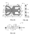
- FIGS. 2A through 2D The bottom heat sink 20 is illustrated in more detail in FIGS. 2A through 2D .
- FIGS. 2A , 2 B, 2 C, and 2 D provide, respectively, a top view, a side view, a front view, and a bottom view of the bottom heat sink 20 of FIG. 1A .
- FIG. 2C also shows an LED assembly 60 in addition to the front view of the bottom heat sink 20 .
- the LED assembly 60 is also illustrated in FIG. 1B .
- the bottom heat sink 20 provides support for electrical traces 22 and 24 ; for solder pads 26 , 32 , and 34 ; and for the LED assembly 60 .
- the bottom heat sink 20 is also referred to as a substrate 20 .
- solder pads 26 , 32 , and 34 are indicated with reference numbers.
- the traces 22 and 24 and the solder pads 32 , 34 , and 36 can be fabricated using conductive material. Further, additional traces and connections can be fabricated on the top, side, or bottom of the substrate 20 , or layered within the substrate 20 .
- the traces 22 and 24 , the solder pads 32 , 34 , and 36 , and any other connections can be interconnected to each other in any combination using known methods, for example via holes.
- the substrate 20 is made of material having high thermal conductivity but is electrically insulating, for example, aluminum nitride (AlN) or alumina (Al 2 O 3 ). Dimensions of the substrate 20 can vary widely depending on application and processes used to manufacture the die package 10 . For example, in the illustrated embodiment, the substrate 20 may have dimensions ranging from fractions of millimeters (mm) to tens of millimeters. Although the present invention is not limited to particular dimensions, one specific embodiment of the die package 10 of the present invention is illustrated in Figures with the dimensions denoted therein. All dimensions shown in the Figures are in millimeters (for lengths, widths, heights, and radii) and degrees (for angles) except as otherwise designated in the Figures, in the Specification herein, or both.
- the substrate 20 has a top surface 21 , the top surface 21 including the electrical traces 22 and 24 .
- the traces 22 and 24 provide electrical connections from the solder pads (for example top solder pads 26 ) to a mounting pad 28 .
- the top solder pads 26 are portions of the traces 22 and 24 generally proximal to sides of the substrate 20 .
- the top solder pads 26 are electrically connected to side solder pads 32 .
- the mounting pad 28 is a portion of the top surface (including portions of the trace 22 , the trace 24 , or both) where the LED assembly 60 is mounted.
- the mounting pad 28 is generally located proximal to center of the top surface 21 .
- the LED assembly 60 can be replaced by other semiconductor circuits or chips.
- the traces 22 and 24 provide electrical routes to allow the LED assembly 60 to electrically connect to the solder pads 26 , 32 , or 34 . Accordingly, some of the traces are referred to as first traces 22 while other traces are referred to as second traces 24 .
- the mounting pad 28 includes portions of both the first traces 22 and the second traces 24 .
- the LED assembly 60 is placed on the first trace 22 portion of the mounting pad 28 , thereby making contact with the first trace 22 .
- a top of the LED assembly 60 and the second traces 24 are connected to each other via a bond wire 62 .
- first traces 22 may provide anode (positive) connections and second traces 24 may comprise cathode (negative) connections for the LED assembly 60 (or vice versa).
- the LED assembly 60 can include additional elements.
- the LED assembly 60 is illustrated including an LED bond wire 62 , an LED subassembly 64 , and a light emitting diode (LED) 66 .
- LED light emitting diode
- Such an LED subassembly 64 is known in the art and is illustrated for the purposes of discussing the invention and is not meant to be a limitation of the present invention.
- the LED assembly 60 is shown die-attached to the substrate 20 .
- the mounting pad 28 can be configured to allow flip-chip attachment of the LED assembly 60 .
- multiple LED assemblies can be mounted on the mounting pad 28 .
- the LED assembly 60 can be mounted over multiple traces. This is especially true if flip-chip technology is used.
- the topology of the traces 22 and 24 can vary widely from the topology illustrated in the Figures while still remaining within the scope of the example embodiments of the present invention.
- three separate cathode (negative) traces 24 are shown to illustrate that three LED assemblies can be placed on the mounting pad 28 , each connected to a different cathode (negative) trace; thus, the three LED assemblies may be separately electrically controllable.
- the traces 22 and 24 are made of conductive material such as gold, silver, tin, or other metals.
- the traces 22 and 24 can have dimensions as illustrated in the Figures and are of a thickness on the order of microns or tens of microns, depending on application. In an example, the traces 22 and 24 can be 15 microns thick.
- FIG. 1A and 2A illustrate an orientation marking 27 . Such markings can be used to identify the proper orientation of the die package 10 even after assembling the die package 10 .
- the traces 22 and 24 as illustrated, can extend from the mounting pad 28 to sides of the substrate 20 .
- the substrate 20 defines semi-cylindrical spaces 23 and quarter-cylindrical spaces 25 proximal to its sides.
- the semi-cylindrical spaces 23 and the quarter-cylindrical spaces 25 provide spaces for solder to flow-through and solidify-in when the die package 10 is attached to a printed circuit board (PCB) or another apparatus (not shown) to which the die package 10 is a component thereof.
- the semi-cylindrical spaces 23 and the quarter-cylindrical spaces 25 provide convenient delineation and break points during the manufacturing process.
- the substrate 20 can be manufactured as one individual section of a strip or a plate having a plurality of adjacent sections, each section being a substrate 20 .
- the substrate 20 can be manufactured as one individual section of an array of sections, the array having multiple rows and columns of adjacent sections.
- the semi-cylindrical spaces 23 and quarter-cylindrical spaces 25 can be utilized as tooling holes for the strip, the plate, or the array during the manufacturing process.
- the semi-cylindrical spaces 23 and the quarter-cylindrical spaces 25 assist in separating each individual substrate from the strip, the plate, or the wafer.
- the separation can be accomplished by introducing physical stress to the perforation (semi through holes at a close pitch) or scribe lines made by laser, or premolded, or etched lines (crossing the semi-cylindrical spaces 23 and the quarter-cylindrical spaces 25 ) by bending the strip, the plate, or the wafer.
- the substrate 20 has a bottom surface 29 including a thermal contact pad 36 .
- the thermal contact pad 36 can be fabricated using a material having a high thermally and electrically conductive properties such as gold, silver, tin, or another material including but not limited to precious metals.
- FIG. 3 illustrates a cut-away side view of portions of the semiconductor package of FIGS. 1A and 1B .
- the FIG. 3 illustrates a cut-away side view of the top heat sink 40 and the lens 50 .
- the top heat sink 40 is made from a material having high thermal conductivity such as aluminum, copper, ceramics, plastics, composites, or a combination of these materials.
- a high temperature, mechanically tough, dielectric material can be used to overcoat the traces 22 and 24 (with the exception of the central die-attach area) to seal the traces 22 and 24 and provide protection from physical and environmental harm such as scratches and oxidation.
- the overcoating process can be a part of the substrate manufacturing process.
- the overcoat when used, may insulate the substrate 20 from the top heat sink 40 .
- the overcoat may then be covered with a high temperature adhesive such as thermal interface material manufactured by THERMOSET that bonds the substrate 20 to the top heat sink 40 .
- the top heat sink 40 may include a reflective surface 42 substantially surrounding the LED assembly 60 mounted on the mounting pad 28 (of FIGS. 2A and 2C ).
- the top heat sink 40 When the top heat sink 40 is used to dissipate heat generated by the LED in the die package 10 , it can be “top-mounted” directly onto an external heat sink by an adhesive or solder joint to dissipate heat efficiently.
- the top heat sink 40 may be equipped with cooling fins or any feature that will enhance heat transfer between the top heat sink 40 and the cooling medium.
- the electrical terminals and the bottom heat sink 20 of the die package 10 can still be connected to its application printed circuit board (PCB) using, for example, the normal surface-mount-technology (SMT) method.
- PCB application printed circuit board
- the reflective surface 42 reflects portions of light from the LED assembly 60 as illustrated by sample light rays 63 . Other portions of the light are not reflected by the reflective surface 42 as illustrated by sample light ray 61 . Illustrative light rays 61 and 63 are not meant to represent light traces often use in the optical arts.
- the top heat sink 40 is preferably made from material that can be polished, coined, molded, or any combination of these. Alternatively, to achieve high reflectivity, the optical reflective surface 42 or the entire heat sink 40 can be plated or deposited with high reflective material such as silver, aluminum, or any substance that serves the purpose. For this reason, the top heat sink 40 is also referred to as a reflector plate 40 .
- the reflector plate 40 is made of material having high thermal conductivity if and when required by the thermal performance of the package 10 .
- the reflective surface 42 is illustrated as a flat surface at an angle, for example 45 degrees, relative to the reflective plate's horizontal plane.
- the example embodiments are not limited to the illustrated embodiment.
- the reflective surface 42 can be at a different angle relative to the reflective plate's horizontal plane.
- the reflective plate can have a parabolic, toroid or any other shape that helps to meet the desired spectral luminous performance of the package.
- the reflective plate 40 includes a ledge 44 for supporting and coupling with the lens 50 .
- the LED assembly 60 is encapsulated within the die package 10 (of FIGS. 1A and 1B ) using encapsulation material 46 such as, for example only, soft and elastic silicones or polymers.
- the encapsulation material 46 can be a high temperature polymer with high light transmissivity and refractive index that matches or closely matches refractive index of the lens 50 , for example.
- the encapsulant 46 is not affected by most wavelengths that alter its light transmissivity or clarity.
- the lens 50 is made from material having high light transmissivity such as, for example only, glass, quartz, high temperature and transparent plastic, or a combination of these materials.
- the lens 50 is placed on top of and adheres to the encapsulation material 46 .
- the lens 50 is not rigidly bonded to the reflector 40 .
- This “floating lens” design enables the encapsulant 46 to expand and contract under high and low temperature conditions without difficulty. For instance, when the die package 10 is operating or being subjected to a high temperature environment, the encapsulant 46 experiences greater volumetric expansion than the cavity space that contains it. By allowing the lens 50 to float up somewhat freely on top of the encapsulant 46 , no encapsulant will be squeezed out of its cavity space.
- the encapsulant 46 when the die package 10 is subjected to a cold temperature, the encapsulant 46 will contract more than the other components that make up the cavity space for the encapsulant 46 ; the lens will float freely on top of the encapsulant 46 as the latter shrinks and its level drops. Hence, the reliability of the die package 10 is maintained over relatively large temperature ranges as the thermal stresses induced on the encapsulant 46 is reduced by the floating lens design.
- the lens 50 defines a recess 52 (See FIG. 3 ) having a curved, hemispherical, or other geometry, which can be filled with optical materials intended to influence or change the nature of the light emitted by the LED chip(s) before it leaves the die package 10 .
- optical materials include luminescence converting phosphors, dyes, fluorescent polymers or other materials which absorb some of the light emitted by the chip(s) and re-emit light of different wavelengths.
- Examples of another type of optical materials include light diffusants such as calcium carbonate, scattering particles (such as Titanium oxides) or voids which disperse or scatter light. Any one or a combination of the above materials can be applied on the lens 50 to obtain certain spectral luminous performance.
- FIG. 4 illustrates the die package 10 coupled to an external heat sink 70 .
- the thermal contact pad 36 can be attached to the external heat sink 70 using epoxy, solder, or any other thermally conductive adhesive, electrically conductive adhesive, or thermally and electrically conductive adhesive 74 .
- the external heat sink 70 can be a printed circuit board (PCB) or other structure that draws heat from the die package 10 .
- the external heat sink can include circuit elements (not shown) or heat dissipation fins 72 in various configurations.
- FIGS. 5 through 6D An example embodiment having an alternate configuration is shown in FIGS. 5 through 6D . Portions of this second embodiment are similar to corresponding portions of the first embodiment illustrated in FIGS. 1A through 4 . For convenience, portions of the second embodiment as illustrated in FIGS. 5 through 6D that are similar to portions of the first embodiment are assigned the same reference numerals, analogous but changed portions are assigned the same reference numerals accompanied by letter “a,” and different portions are assigned different reference numerals.
- FIG. 5 is an exploded perspective view of an LED die package 10 a in accordance with other embodiments of the present invention.
- the light emitting die package 10 a of the present invention includes a bottom heat sink (substrate) 20 a , a top heat sink (reflector plate) 40 a , and a lens 50 .
- FIGS. 6A , 6 B, 6 C, and 6 D provide, respectively, a top view, a side view, a front view, and a bottom view of the substrate 20 a of FIG. 5 .
- the substrate 20 a includes one first trace 22 a and four second traces 24 a . Traces 22 a and 24 a are configured differently than traces 22 and 24 of FIG. 2A .
- the substrate 20 a includes flanges 31 that define latch spaces 33 for reception of legs 35 of the reflector plate 40 a , thereby mechanically engaging the reflector plate 40 a with the substrate 20 a.
Abstract
Description
Claims (19)
Priority Applications (1)
| Application Number | Priority Date | Filing Date | Title |
|---|---|---|---|
| US13/023,273 US8622582B2 (en) | 2002-09-04 | 2011-02-08 | Power surface mount light emitting die package |
Applications Claiming Priority (5)
| Application Number | Priority Date | Filing Date | Title |
|---|---|---|---|
| US40825402P | 2002-09-04 | 2002-09-04 | |
| US10/446,532 US7264378B2 (en) | 2002-09-04 | 2003-05-27 | Power surface mount light emitting die package |
| US11/703,721 US7775685B2 (en) | 2003-05-27 | 2007-02-08 | Power surface mount light emitting die package |
| US12/856,320 US7976186B2 (en) | 2003-05-27 | 2010-08-13 | Power surface mount light emitting die package |
| US13/023,273 US8622582B2 (en) | 2002-09-04 | 2011-02-08 | Power surface mount light emitting die package |
Related Parent Applications (1)
| Application Number | Title | Priority Date | Filing Date |
|---|---|---|---|
| US12/856,320 Division US7976186B2 (en) | 2002-09-04 | 2010-08-13 | Power surface mount light emitting die package |
Publications (2)
| Publication Number | Publication Date |
|---|---|
| US20110186897A1 US20110186897A1 (en) | 2011-08-04 |
| US8622582B2 true US8622582B2 (en) | 2014-01-07 |
Family
ID=38172439
Family Applications (6)
| Application Number | Title | Priority Date | Filing Date |
|---|---|---|---|
| US11/703,721 Expired - Lifetime US7775685B2 (en) | 2002-09-04 | 2007-02-08 | Power surface mount light emitting die package |
| US11/694,046 Expired - Lifetime US7659551B2 (en) | 2003-05-27 | 2007-03-30 | Power surface mount light emitting die package |
| US12/856,320 Expired - Lifetime US7976186B2 (en) | 2002-09-04 | 2010-08-13 | Power surface mount light emitting die package |
| US13/023,273 Expired - Lifetime US8622582B2 (en) | 2002-09-04 | 2011-02-08 | Power surface mount light emitting die package |
| US13/023,268 Expired - Lifetime US8167463B2 (en) | 2002-09-04 | 2011-02-08 | Power surface mount light emitting die package |
| US13/023,263 Expired - Lifetime US8608349B2 (en) | 2002-09-04 | 2011-02-08 | Power surface mount light emitting die package |
Family Applications Before (3)
| Application Number | Title | Priority Date | Filing Date |
|---|---|---|---|
| US11/703,721 Expired - Lifetime US7775685B2 (en) | 2002-09-04 | 2007-02-08 | Power surface mount light emitting die package |
| US11/694,046 Expired - Lifetime US7659551B2 (en) | 2003-05-27 | 2007-03-30 | Power surface mount light emitting die package |
| US12/856,320 Expired - Lifetime US7976186B2 (en) | 2002-09-04 | 2010-08-13 | Power surface mount light emitting die package |
Family Applications After (2)
| Application Number | Title | Priority Date | Filing Date |
|---|---|---|---|
| US13/023,268 Expired - Lifetime US8167463B2 (en) | 2002-09-04 | 2011-02-08 | Power surface mount light emitting die package |
| US13/023,263 Expired - Lifetime US8608349B2 (en) | 2002-09-04 | 2011-02-08 | Power surface mount light emitting die package |
Country Status (1)
| Country | Link |
|---|---|
| US (6) | US7775685B2 (en) |
Cited By (3)
| Publication number | Priority date | Publication date | Assignee | Title |
|---|---|---|---|---|
| US20140120746A1 (en) * | 2012-10-24 | 2014-05-01 | Rostislav Persion | Electrical and fiber optic connector with magnetic electrical contacts |
| US10683971B2 (en) | 2015-04-30 | 2020-06-16 | Cree, Inc. | Solid state lighting components |
| US10797204B2 (en) | 2014-05-30 | 2020-10-06 | Cree, Inc. | Submount based light emitter components and methods |
Families Citing this family (94)
| Publication number | Priority date | Publication date | Assignee | Title |
|---|---|---|---|---|
| US8545629B2 (en) | 2001-12-24 | 2013-10-01 | Crystal Is, Inc. | Method and apparatus for producing large, single-crystals of aluminum nitride |
| US7244965B2 (en) * | 2002-09-04 | 2007-07-17 | Cree Inc, | Power surface mount light emitting die package |
| US7775685B2 (en) * | 2003-05-27 | 2010-08-17 | Cree, Inc. | Power surface mount light emitting die package |
| US7980743B2 (en) * | 2005-06-14 | 2011-07-19 | Cree, Inc. | LED backlighting for displays |
| US20060292747A1 (en) * | 2005-06-27 | 2006-12-28 | Loh Ban P | Top-surface-mount power light emitter with integral heat sink |
| KR100629496B1 (en) * | 2005-08-08 | 2006-09-28 | 삼성전자주식회사 | Led package structure and manufacturing method for the same |
| WO2007065018A2 (en) | 2005-12-02 | 2007-06-07 | Crystal Is, Inc. | Doped aluminum nitride crystals and methods of making them |
| US9034103B2 (en) | 2006-03-30 | 2015-05-19 | Crystal Is, Inc. | Aluminum nitride bulk crystals having high transparency to ultraviolet light and methods of forming them |
| JP2007311445A (en) * | 2006-05-17 | 2007-11-29 | Stanley Electric Co Ltd | Semiconductor light-emitting device, and manufacturing method thereof |
| US20090185381A1 (en) * | 2006-05-23 | 2009-07-23 | Koninklijke Philips Electronics N.V. | Automotive lamp module and lighting unit with led lighting element |
| US9771666B2 (en) | 2007-01-17 | 2017-09-26 | Crystal Is, Inc. | Defect reduction in seeded aluminum nitride crystal growth |
| CN107059116B (en) | 2007-01-17 | 2019-12-31 | 晶体公司 | Defect reduction in seeded aluminum nitride crystal growth |
| US8080833B2 (en) | 2007-01-26 | 2011-12-20 | Crystal Is, Inc. | Thick pseudomorphic nitride epitaxial layers |
| US20090323341A1 (en) * | 2007-06-28 | 2009-12-31 | Boundary Net, Incorporated | Convective cooling based lighting fixtures |
| US20090002362A1 (en) | 2007-06-28 | 2009-01-01 | Boundary Net, Incorporated | Image to temporal pixel mapping |
| JP2009081428A (en) * | 2007-09-03 | 2009-04-16 | Rohm Co Ltd | Semiconductor light emitting device and method of manufacturing the same |
| CN101469845B (en) * | 2007-12-29 | 2011-08-24 | 富士迈半导体精密工业(上海)有限公司 | Illuminating apparatus, power supply module group thereof and lamp with the illuminating apparatus |
| TW200937597A (en) * | 2008-02-20 | 2009-09-01 | Chipmos Technologies Inc | Quad flat non-leaded package structure |
| US9022612B2 (en) * | 2008-08-07 | 2015-05-05 | Mag Instrument, Inc. | LED module |
| CN101660716A (en) * | 2008-08-25 | 2010-03-03 | 富士迈半导体精密工业(上海)有限公司 | Light source device |
| US8598602B2 (en) * | 2009-01-12 | 2013-12-03 | Cree, Inc. | Light emitting device packages with improved heat transfer |
| US7923739B2 (en) * | 2009-06-05 | 2011-04-12 | Cree, Inc. | Solid state lighting device |
| US20100237364A1 (en) * | 2009-03-19 | 2010-09-23 | Christy Alexander C | Thermal Energy Dissipating and Light Emitting Diode Mounting Arrangement |
| US8089075B2 (en) * | 2009-04-17 | 2012-01-03 | Avago Technologies Ecbu Ip (Singapore) Pte. Ltd. | LFCC package with a reflector cup surrounded by a single encapsulant |
| US8101955B2 (en) * | 2009-04-17 | 2012-01-24 | Avago Technologies Ecbu Ip (Singapore) Pte. Ltd. | PLCC package with a reflector cup surrounded by an encapsulant |
| US9269875B2 (en) * | 2009-05-20 | 2016-02-23 | Intellectual Discovery Co., Ltd. | Light emitter |
| US20100302788A1 (en) * | 2009-05-28 | 2010-12-02 | Chia-Cheng Chang | Light emitting diode lamp-set |
| US8860043B2 (en) * | 2009-06-05 | 2014-10-14 | Cree, Inc. | Light emitting device packages, systems and methods |
| US8686445B1 (en) | 2009-06-05 | 2014-04-01 | Cree, Inc. | Solid state lighting devices and methods |
| US9111778B2 (en) | 2009-06-05 | 2015-08-18 | Cree, Inc. | Light emitting diode (LED) devices, systems, and methods |
| WO2010151600A1 (en) | 2009-06-27 | 2010-12-29 | Michael Tischler | High efficiency leds and led lamps |
| EP2816677B1 (en) * | 2009-09-18 | 2020-04-01 | Intel Corporation | Combined optical and electrical interface |
| TWI408310B (en) * | 2009-09-29 | 2013-09-11 | Liang Meng Plastic Share Co Ltd | Illuminating device and method for manufacturing the same |
| US9480133B2 (en) | 2010-01-04 | 2016-10-25 | Cooledge Lighting Inc. | Light-emitting element repair in array-based lighting devices |
| US8653539B2 (en) | 2010-01-04 | 2014-02-18 | Cooledge Lighting, Inc. | Failure mitigation in arrays of light-emitting devices |
| US8269244B2 (en) | 2010-06-28 | 2012-09-18 | Cree, Inc. | LED package with efficient, isolated thermal path |
| US8648359B2 (en) | 2010-06-28 | 2014-02-11 | Cree, Inc. | Light emitting devices and methods |
| KR101372084B1 (en) | 2010-06-29 | 2014-03-07 | 쿨레지 라이팅 인크. | Electronic devices with yielding substrates |
| CN105951177B (en) | 2010-06-30 | 2018-11-02 | 晶体公司 | Use the growth for the bulk aluminum nitride single crystal that thermal gradient controls |
| USD643819S1 (en) | 2010-07-16 | 2011-08-23 | Cree, Inc. | Package for light emitting diode (LED) lighting |
| US8565562B2 (en) | 2010-09-21 | 2013-10-22 | Intel Corporation | Connector optical lens with alignment features |
| MY170920A (en) | 2010-11-02 | 2019-09-17 | Carsem M Sdn Bhd | Leadframe package with recessed cavity for led |
| USD679842S1 (en) | 2011-01-03 | 2013-04-09 | Cree, Inc. | High brightness LED package |
| US11101408B2 (en) | 2011-02-07 | 2021-08-24 | Creeled, Inc. | Components and methods for light emitting diode (LED) lighting |
| US8610140B2 (en) * | 2010-12-15 | 2013-12-17 | Cree, Inc. | Light emitting diode (LED) packages, systems, devices and related methods |
| TWM405642U (en) * | 2010-12-30 | 2011-06-11 | Forward Electronics Co Ltd | Trichromatic light emitting diode module |
| CN102588762A (en) * | 2011-01-06 | 2012-07-18 | 隆达电子股份有限公司 | LED cup lamp |
| TWI414714B (en) | 2011-04-15 | 2013-11-11 | Lextar Electronics Corp | Light emitting diode cup light |
| US20120188738A1 (en) * | 2011-01-25 | 2012-07-26 | Conexant Systems, Inc. | Integrated led in system-in-package module |
| TW201251140A (en) | 2011-01-31 | 2012-12-16 | Cree Inc | High brightness light emitting diode (LED) packages, systems and methods with improved resin filling and high adhesion |
| US9209373B2 (en) * | 2011-02-23 | 2015-12-08 | Intellectual Discovery Co., Ltd. | High power plastic leaded chip carrier with integrated metal reflector cup and direct heat sink |
| US20120236532A1 (en) * | 2011-03-14 | 2012-09-20 | Koo Won-Hoe | Led engine for illumination |
| EP2695189A1 (en) * | 2011-04-04 | 2014-02-12 | CeramTec GmbH | Ceramic printed circuit board comprising an al cooling body |
| TW201251132A (en) * | 2011-05-03 | 2012-12-16 | Cree Inc | Light emitting diode (LED) packages, systems, devices and related methods |
| US20120286297A1 (en) * | 2011-05-09 | 2012-11-15 | Taiwan Micropaq Corporation | Led package structure and module thereof |
| US8962359B2 (en) | 2011-07-19 | 2015-02-24 | Crystal Is, Inc. | Photon extraction from nitride ultraviolet light-emitting devices |
| CN102954366B (en) * | 2011-08-16 | 2016-06-22 | 惠州元晖光电股份有限公司 | There is the photo engine of light switching array |
| US8853726B2 (en) * | 2011-08-25 | 2014-10-07 | Lg Innotek Co., Ltd. | Light emitting device package and lighting system having the same |
| KR101817807B1 (en) * | 2011-09-20 | 2018-01-11 | 엘지이노텍 주식회사 | Light emitting device package and lighting system including the same |
| MY156107A (en) | 2011-11-01 | 2016-01-15 | Carsem M Sdn Bhd | Large panel leadframe |
| US8939611B2 (en) * | 2011-11-10 | 2015-01-27 | Tsmc Solid State Lighting Ltd. | Lighting apparatus having improved light output uniformity and thermal dissipation |
| JP2013131744A (en) * | 2011-11-25 | 2013-07-04 | Citizen Electronics Co Ltd | Method for mounting light emitting element, and light emitting device including light emitting element |
| CN104025323B (en) * | 2011-12-21 | 2017-12-26 | 英特尔公司 | Heat management for light emitting diode |
| US8564012B2 (en) | 2012-02-10 | 2013-10-22 | Intersil Americas LLC | Optoelectronic apparatuses and methods for manufacturing optoelectronic apparatuses |
| US8783911B2 (en) * | 2012-02-17 | 2014-07-22 | Tsmc Solid State Lighting Ltd. | LED packaging structure having improved thermal dissipation and mechanical strength |
| US8796052B2 (en) | 2012-02-24 | 2014-08-05 | Intersil Americas LLC | Optoelectronic apparatuses with post-molded reflector cups and methods for manufacturing the same |
| US9541258B2 (en) | 2012-02-29 | 2017-01-10 | Cree, Inc. | Lens for wide lateral-angle distribution |
| US10408429B2 (en) | 2012-02-29 | 2019-09-10 | Ideal Industries Lighting Llc | Lens for preferential-side distribution |
| US9541257B2 (en) | 2012-02-29 | 2017-01-10 | Cree, Inc. | Lens for primarily-elongate light distribution |
| WO2013169643A1 (en) * | 2012-05-07 | 2013-11-14 | Cree, Inc. | Lens for wide lateral-angle distribution |
| US9011022B2 (en) | 2012-05-29 | 2015-04-21 | Intel Corporation | Combined optical and electrical interface |
| CN102818216B (en) * | 2012-06-05 | 2014-08-06 | 佛山市国星光电股份有限公司 | Large-angle lens and large-angle light-emergent LED (Light Emitting Diode) light source module |
| US8877561B2 (en) | 2012-06-07 | 2014-11-04 | Cooledge Lighting Inc. | Methods of fabricating wafer-level flip chip device packages |
| WO2014047268A1 (en) | 2012-09-19 | 2014-03-27 | Venntis Technologies LLC | Illuminator with device for scattering light |
| US9595627B2 (en) | 2013-03-15 | 2017-03-14 | John Paul Morgan | Photovoltaic panel |
| USD718490S1 (en) * | 2013-03-15 | 2014-11-25 | Cree, Inc. | LED lens |
| WO2014151264A1 (en) | 2013-03-15 | 2014-09-25 | Crystal Is, Inc. | Planar contacts to pseudomorphic electronic and optoelectronic devices |
| US9960303B2 (en) | 2013-03-15 | 2018-05-01 | Morgan Solar Inc. | Sunlight concentrating and harvesting device |
| US9714756B2 (en) | 2013-03-15 | 2017-07-25 | Morgan Solar Inc. | Illumination device |
| US9080746B2 (en) | 2013-03-15 | 2015-07-14 | Abl Ip Holding Llc | LED assembly having a refractor that provides improved light control |
| EP2971950B1 (en) | 2013-03-15 | 2021-05-19 | Morgan Solar Inc. | Light panel, optical assembly with improved interface and light panel with improved manufacturing tolerances |
| EP3105300B1 (en) | 2014-02-13 | 2019-08-21 | Honeywell International Inc. | Compressible thermal interface materials |
| USD762321S1 (en) * | 2014-10-22 | 2016-07-26 | Phoenix Products Company, Inc. | Light fixture |
| EP3064166B1 (en) * | 2015-03-06 | 2018-07-04 | Schott AG | Hermetically sealed led light, and method for manufacturing a hermetically sealed led light |
| USD912303S1 (en) * | 2015-04-07 | 2021-03-02 | Flos S.P.A. | Table lamp |
| US9512978B1 (en) | 2015-08-13 | 2016-12-06 | Randal L Wimberly | Vortex light projection system, LED lensless primary optics system, and perfectly random LED color mixing system |
| CN106549088B (en) * | 2015-09-17 | 2018-11-16 | 光宝光电(常州)有限公司 | Light emitting display device |
| US9903561B1 (en) | 2015-11-09 | 2018-02-27 | Abl Ip Holding Llc | Asymmetric vision enhancement optics, luminaires providing asymmetric light distributions and associated methods |
| US10781349B2 (en) | 2016-03-08 | 2020-09-22 | Honeywell International Inc. | Thermal interface material including crosslinker and multiple fillers |
| US11041103B2 (en) | 2017-09-08 | 2021-06-22 | Honeywell International Inc. | Silicone-free thermal gel |
| US11072706B2 (en) | 2018-02-15 | 2021-07-27 | Honeywell International Inc. | Gel-type thermal interface material |
| US11227985B2 (en) * | 2019-03-28 | 2022-01-18 | Nichia Corporation | Light-emitting device |
| US11373921B2 (en) | 2019-04-23 | 2022-06-28 | Honeywell International Inc. | Gel-type thermal interface material with low pre-curing viscosity and elastic properties post-curing |
| US10986722B1 (en) * | 2019-11-15 | 2021-04-20 | Goodrich Corporation | High performance heat sink for double sided printed circuit boards |
Citations (149)
| Publication number | Priority date | Publication date | Assignee | Title |
|---|---|---|---|---|
| US3443140A (en) | 1965-04-06 | 1969-05-06 | Gen Electric | Light emitting semiconductor devices of improved transmission characteristics |
| US3760237A (en) | 1972-06-21 | 1973-09-18 | Gen Electric | Solid state lamp assembly having conical light director |
| US4152618A (en) | 1977-04-05 | 1979-05-01 | Tokyo Shibaura Electric Co., Ltd. | Light-emitting display device including light diffusing film |
| US4168102A (en) | 1976-10-12 | 1979-09-18 | Tokyo Shibaura Electric Co., Ltd. | Light-emitting display device including a light diffusing bonding layer |
| US4267559A (en) | 1979-09-24 | 1981-05-12 | Bell Telephone Laboratories, Incorporated | Low thermal impedance light-emitting diode package |
| US4603496A (en) | 1985-02-04 | 1986-08-05 | Adaptive Micro Systems, Inc. | Electronic display with lens matrix |
| US5119174A (en) | 1990-10-26 | 1992-06-02 | Chen Der Jong | Light emitting diode display with PCB base |
| US5173839A (en) | 1990-12-10 | 1992-12-22 | Grumman Aerospace Corporation | Heat-dissipating method and device for led display |
| US5285352A (en) * | 1992-07-15 | 1994-02-08 | Motorola, Inc. | Pad array semiconductor device with thermal conductor and process for making the same |
| US5433295A (en) | 1993-02-04 | 1995-07-18 | Inventio Ag | Indicating element for elevators |
| US5633963A (en) | 1995-12-12 | 1997-05-27 | Raytheon Company | Optical rotary joint for single and multimode fibers |
| US5649757A (en) | 1994-11-04 | 1997-07-22 | Aleman; Thomas M. | Aquarium background illuminator |
| US5785418A (en) | 1996-06-27 | 1998-07-28 | Hochstein; Peter A. | Thermally protected LED array |
| US5789772A (en) | 1994-07-15 | 1998-08-04 | The Whitaker Corporation | Semi-insulating surface light emitting devices |
| US5835661A (en) | 1994-10-19 | 1998-11-10 | Tai; Ping-Kaung | Light expanding system for producing a linear or planar light beam from a point-like light source |
| US5841177A (en) | 1993-06-25 | 1998-11-24 | Kabushiki Kaisha Toshiba | Multicolor light emitting device |
| JPH10321909A (en) | 1997-05-19 | 1998-12-04 | Nichia Chem Ind Ltd | Semiconductor device |
| US5847507A (en) | 1997-07-14 | 1998-12-08 | Hewlett-Packard Company | Fluorescent dye added to epoxy of light emitting diode lens |
| US5849396A (en) | 1995-09-13 | 1998-12-15 | Hughes Electronics Corporation | Multilayer electronic structure and its preparation |
| US5851847A (en) | 1995-09-29 | 1998-12-22 | Sony Corporation | Photonic device and process for fabricating the same |
| US5857767A (en) | 1996-09-23 | 1999-01-12 | Relume Corporation | Thermal management system for L.E.D. arrays |
| US5869883A (en) | 1997-09-26 | 1999-02-09 | Stanley Wang, President Pantronix Corp. | Packaging of semiconductor circuit in pre-molded plastic package |
| US5903052A (en) * | 1998-05-12 | 1999-05-11 | Industrial Technology Research Institute | Structure for semiconductor package for improving the efficiency of spreading heat |
| US5907151A (en) | 1996-05-24 | 1999-05-25 | Siemens Aktiengesellschaft | Surface mountable optoelectronic transducer and method for its production |
| JPH11177136A (en) | 1997-12-15 | 1999-07-02 | Nichia Chem Ind Ltd | Chip type led |
| US5959316A (en) | 1998-09-01 | 1999-09-28 | Hewlett-Packard Company | Multiple encapsulation of phosphor-LED devices |
| US5982090A (en) | 1997-07-11 | 1999-11-09 | Kaiser Aerospace And Electronics Coporation | Integrated dual mode flat backlight |
| US5998925A (en) | 1996-07-29 | 1999-12-07 | Nichia Kagaku Kogyo Kabushiki Kaisha | Light emitting device having a nitride compound semiconductor and a phosphor containing a garnet fluorescent material |
| JP2000013962A (en) | 1998-06-16 | 2000-01-14 | Sumitomo Wiring Syst Ltd | Electric junction box |
| DE19945919A1 (en) | 1998-09-25 | 2000-03-30 | Rohm Co Ltd | Light emitting semiconductor device has an epoxy resin encapsulation of low glass transition temperature to reduce crack-inducing thermal stresses on surface mounting of the device e.g. on a wiring board |
| US6060729A (en) | 1997-11-26 | 2000-05-09 | Rohm Co., Ltd. | Light-emitting device |
| JP2000236116A (en) | 1999-02-15 | 2000-08-29 | Matsushita Electric Works Ltd | Light source equipment |
| US6124635A (en) | 1997-03-21 | 2000-09-26 | Honda Giken Kogyo Kabushiki Kaisha | Functionally gradient integrated metal-ceramic member and semiconductor circuit substrate application thereof |
| JP2000277807A (en) | 1999-01-01 | 2000-10-06 | Sanken Electric Co Ltd | Outer lens for semiconductor light emitting module |
| US6155699A (en) | 1999-03-15 | 2000-12-05 | Agilent Technologies, Inc. | Efficient phosphor-conversion led structure |
| EP1059678A2 (en) | 1999-06-09 | 2000-12-13 | Sanyo Electric Co., Ltd. | Hybrid integrated circuit device |
| US6180962B1 (en) | 1998-10-23 | 2001-01-30 | Rohm Co., Ltd. | Chip type semiconductor light emitting device having a solder preventive portion |
| JP2001036148A (en) | 1999-07-23 | 2001-02-09 | Matsushita Electric Works Ltd | Light source |
| JP2001044452A (en) | 1999-08-03 | 2001-02-16 | Sony Corp | Optical communication module |
| JP2001052513A (en) | 1999-08-04 | 2001-02-23 | Hamamatsu Photonics Kk | Floodlight |
| EP1087447A1 (en) | 1999-03-18 | 2001-03-28 | Rohm Co., Ltd. | Light-emitting semiconductor chip |
| JP2001111117A (en) | 1999-09-03 | 2001-04-20 | Agilent Technol Inc | Light emitting device using light emitting diodes and manufacturing method thereof |
| JP2001111116A (en) | 1999-10-13 | 2001-04-20 | Rohm Co Ltd | Chip type semiconductor light emitting device |
| JP2001144333A (en) | 1999-11-10 | 2001-05-25 | Sharp Corp | Light-emitting device and manufacturing method therefor |
| US6238599B1 (en) | 1997-06-18 | 2001-05-29 | International Business Machines Corporation | High conductivity, high strength, lead-free, low cost, electrically conducting materials and applications |
| US6274924B1 (en) | 1998-11-05 | 2001-08-14 | Lumileds Lighting, U.S. Llc | Surface mountable LED package |
| US6281435B1 (en) | 1999-03-03 | 2001-08-28 | Rohm Co., Ltd. | Chip-type electronic devices |
| US6307272B1 (en) | 1998-05-27 | 2001-10-23 | Hitachi, Ltd. | Semiconductor device and method for manufacturing the same |
| US6318886B1 (en) | 2000-02-11 | 2001-11-20 | Whelen Engineering Company | High flux led assembly |
| JP2001326390A (en) | 2000-05-18 | 2001-11-22 | Rohm Co Ltd | Rear-surface light-emitting chip type light-emitting element and insulating board used therefor |
| US6329706B1 (en) | 1999-08-24 | 2001-12-11 | Fairchild Korea Semiconductor, Ltd. | Leadframe using chip pad as heat conducting path and semiconductor package adopting the same |
| US6331063B1 (en) | 1997-11-25 | 2001-12-18 | Matsushita Electric Works, Ltd. | LED luminaire with light control means |
| US6335548B1 (en) * | 1999-03-15 | 2002-01-01 | Gentex Corporation | Semiconductor radiation emitter package |
| US6362964B1 (en) | 1999-11-17 | 2002-03-26 | International Rectifier Corp. | Flexible power assembly |
| JP2002093206A (en) | 2000-09-18 | 2002-03-29 | Stanley Electric Co Ltd | Led signal light |
| JP2002103977A (en) | 2000-09-29 | 2002-04-09 | Johnan Seisakusho Co Ltd | Sunroof device for vehicle |
| USRE37707E1 (en) | 1990-02-22 | 2002-05-21 | Stmicroelectronics S.R.L. | Leadframe with heat dissipator connected to S-shaped fingers |
| JP2002185046A (en) | 2000-12-19 | 2002-06-28 | Sharp Corp | Chip-part type led and its manufacturing method |
| US20020084462A1 (en) | 2000-09-29 | 2002-07-04 | Shingo Tamai | Light emission device |
| US20020093206A1 (en) * | 2001-01-12 | 2002-07-18 | Schlage Lock Company | Door latching mechanism |
| TW497758U (en) | 2001-07-02 | 2002-08-01 | Chiou-Sen Hung | Improvement of surface mounted light emitting diode structure |
| US6429513B1 (en) | 2001-05-25 | 2002-08-06 | Amkor Technology, Inc. | Active heat sink for cooling a semiconductor chip |
| US6444498B1 (en) | 2001-08-08 | 2002-09-03 | Siliconware Precision Industries Co., Ltd | Method of making semiconductor package with heat spreader |
| JP2002270903A (en) | 2001-03-08 | 2002-09-20 | Rohm Co Ltd | Back emission chip-type light emitting device |
| US6456766B1 (en) | 2000-02-01 | 2002-09-24 | Cornell Research Foundation Inc. | Optoelectronic packaging |
| US6457645B1 (en) | 1999-04-13 | 2002-10-01 | Hewlett-Packard Company | Optical assembly having lens offset from optical axis |
| US6469322B1 (en) | 1998-02-06 | 2002-10-22 | General Electric Company | Green emitting phosphor for use in UV light emitting diodes |
| US6468821B2 (en) | 1999-01-11 | 2002-10-22 | Matsushita Electric Industrial Co., Ltd. | Method for fabricating semiconductor light-emitting unit |
| JP2002319711A (en) | 2001-04-20 | 2002-10-31 | Citizen Electronics Co Ltd | Surface mounting type light-emitting diode and method for manufacturing the same |
| USD465207S1 (en) | 2001-06-08 | 2002-11-05 | Gem Services, Inc. | Leadframe matrix for a surface mount package |
| US6480389B1 (en) * | 2002-01-04 | 2002-11-12 | Opto Tech Corporation | Heat dissipation structure for solid-state light emitting device package |
| US6489637B1 (en) | 1999-06-09 | 2002-12-03 | Sanyo Electric Co., Ltd. | Hybrid integrated circuit device |
| US6490104B1 (en) | 2000-09-15 | 2002-12-03 | Three-Five Systems, Inc. | Illumination system for a micro display |
| US6492725B1 (en) | 2000-02-04 | 2002-12-10 | Lumileds Lighting, U.S., Llc | Concentrically leaded power semiconductor device package |
| JP2002368278A (en) | 2001-06-06 | 2002-12-20 | Citizen Electronics Co Ltd | Light-emitting diode |
| US6501103B1 (en) | 2001-10-23 | 2002-12-31 | Lite-On Electronics, Inc. | Light emitting diode assembly with low thermal resistance |
| TW517402B (en) | 2001-04-12 | 2003-01-11 | Matsushita Electric Works Ltd | Light source using light emitting diode and method for producing the same |
| TW518775B (en) | 2002-01-29 | 2003-01-21 | Chi-Hsing Hsu | Immersion cooling type light emitting diode and its packaging method |
| US6525386B1 (en) | 1998-03-10 | 2003-02-25 | Masimo Corporation | Non-protruding optoelectronic lens |
| US6531328B1 (en) * | 2001-10-11 | 2003-03-11 | Solidlite Corporation | Packaging of light-emitting diode |
| US20030058650A1 (en) | 2001-09-25 | 2003-03-27 | Kelvin Shih | Light emitting diode with integrated heat dissipater |
| US20030057573A1 (en) | 2001-09-26 | 2003-03-27 | Kabushiki Kaisha Toshiba | Semiconductor device |
| US6541800B2 (en) | 2001-02-22 | 2003-04-01 | Weldon Technologies, Inc. | High power LED |
| JP2003110146A (en) | 2001-07-26 | 2003-04-11 | Matsushita Electric Works Ltd | Light-emitting device |
| JP2003124525A (en) | 2001-10-09 | 2003-04-25 | Agilent Technologies Japan Ltd | Light emitting diode and its manufacturing method |
| US6559525B2 (en) | 2000-01-13 | 2003-05-06 | Siliconware Precision Industries Co., Ltd. | Semiconductor package having heat sink at the outer surface |
| TW533604B (en) | 2000-12-28 | 2003-05-21 | Toyoda Gosei Kk | Light emitting device |
| US6582103B1 (en) | 1996-12-12 | 2003-06-24 | Teledyne Lighting And Display Products, Inc. | Lighting apparatus |
| JP2003197974A (en) | 2001-12-24 | 2003-07-11 | Samsung Electro Mech Co Ltd | Light emitting diode package |
| US6610563B1 (en) | 1997-12-15 | 2003-08-26 | Osram Opto Semiconductors Gmbh & Co. Ohg | Surface mounting optoelectronic component and method for producing same |
| US6614103B1 (en) | 2000-09-01 | 2003-09-02 | General Electric Company | Plastic packaging of LED arrays |
| TW556364B (en) | 2001-08-28 | 2003-10-01 | Matsushita Electric Works Ltd | Light emitting device using LED |
| US20030193083A1 (en) | 2002-04-15 | 2003-10-16 | Citizen Electronics Co., Ltd. | Substrate for light emitting diodes |
| JP2003298117A (en) | 2002-04-05 | 2003-10-17 | Toyoda Gosei Co Ltd | Light emitting diode |
| JP2003318448A (en) | 2002-02-19 | 2003-11-07 | Nichia Chem Ind Ltd | Light emitting device and its forming method |
| US6670648B2 (en) | 2001-07-19 | 2003-12-30 | Rohm Co., Ltd. | Semiconductor light-emitting device having a reflective case |
| US6672734B2 (en) | 2000-10-25 | 2004-01-06 | Lumileds Lighting U.S., Llc | Illumination system and display device |
| US6680491B2 (en) | 2000-02-01 | 2004-01-20 | Matsushita Electric Industrial Co., Ltd. | Optical electronic apparatus and method for producing the same |
| US6680568B2 (en) | 2000-02-09 | 2004-01-20 | Nippon Leiz Corporation | Light source |
| US20040023552A1 (en) * | 2002-07-30 | 2004-02-05 | Wilson Chen | Serial ATA cable |
| US6710544B2 (en) | 2001-02-07 | 2004-03-23 | Patent-Treuhand-Gesellschaft für elektrische Glühiampen mbH | Reflector-containing semiconductor component |
| EP1416219A1 (en) | 2001-08-09 | 2004-05-06 | Matsushita Electric Industrial Co., Ltd. | Led illuminator and card type led illuminating light source |
| US6759803B2 (en) | 1999-04-22 | 2004-07-06 | Osram Opto Semiconductors Gmbh & Co. Ohg | LED light source with lens and corresponding production method |
| US6768525B2 (en) | 2000-12-01 | 2004-07-27 | Lumileds Lighting U.S. Llc | Color isolated backlight for an LCD |
| US6789921B1 (en) | 2003-03-25 | 2004-09-14 | Rockwell Collins | Method and apparatus for backlighting a dual mode liquid crystal display |
| US6791259B1 (en) | 1998-11-30 | 2004-09-14 | General Electric Company | Solid state illumination system containing a light emitting diode, a light scattering material and a luminescent material |
| US20040222433A1 (en) | 2003-05-05 | 2004-11-11 | Lamina Ceramics | Light emitting diodes packaged for high temperature operation |
| US20050001433A1 (en) | 2003-04-30 | 2005-01-06 | Seelink Technology Corporation | Display system having uniform luminosity and wind generator |
| US6844903B2 (en) | 2001-04-04 | 2005-01-18 | Lumileds Lighting U.S., Llc | Blue backlight and phosphor layer for a color LCD |
| US6849867B2 (en) | 1999-03-15 | 2005-02-01 | Gentex Corporation | Method of making radiation emitter devices |
| US20050043627A1 (en) * | 2003-07-17 | 2005-02-24 | Angelsen Bjorn A.J. | Curved ultrasound transducer arrays manufactured with planar technology |
| US6864567B2 (en) | 2003-03-06 | 2005-03-08 | San-Hua Yu | Base of LED |
| US20050093430A1 (en) | 2003-02-26 | 2005-05-05 | Cree, Inc. | Composite white light source and method for fabricating |
| US6897486B2 (en) | 2002-12-06 | 2005-05-24 | Ban P. Loh | LED package die having a small footprint |
| US6903380B2 (en) | 2003-04-11 | 2005-06-07 | Weldon Technologies, Inc. | High power light emitting diode |
| US20050152146A1 (en) | 2002-05-08 | 2005-07-14 | Owen Mark D. | High efficiency solid-state light source and methods of use and manufacture |
| US6943433B2 (en) | 2002-03-06 | 2005-09-13 | Nichia Corporation | Semiconductor device and manufacturing method for same |
| US6960878B2 (en) | 2001-01-24 | 2005-11-01 | Nichia Corporation | Light emitting diode, optical semiconductor element and epoxy resin composition suitable for optical semiconductor element and production methods therefor |
| US20050265029A1 (en) | 2004-06-01 | 2005-12-01 | 3M Innovative Properties Company | Led array systems |
| US7002727B2 (en) | 2003-03-31 | 2006-02-21 | Reflectivity, Inc. | Optical materials in packaging micromirror devices |
| JP2003124528A5 (en) | 2002-08-08 | 2006-04-06 | ||
| US20060083017A1 (en) | 2004-10-18 | 2006-04-20 | Bwt Propety, Inc. | Solid-state lighting apparatus for navigational aids |
| US20060097385A1 (en) | 2004-10-25 | 2006-05-11 | Negley Gerald H | Solid metal block semiconductor light emitting device mounting substrates and packages including cavities and heat sinks, and methods of packaging same |
| US20060098441A1 (en) | 2004-11-05 | 2006-05-11 | Au Optronics Corp. | Backlight module |
| US7044620B2 (en) | 2004-04-30 | 2006-05-16 | Guide Corporation | LED assembly with reverse circuit board |
| US7078728B2 (en) | 2003-07-29 | 2006-07-18 | Citizen Electronics Co., Ltd. | Surface-mounted LED and light emitting device |
| US7084435B2 (en) | 2001-07-26 | 2006-08-01 | Matsushita Electric Works, Ltd. | Light emitting device using LED |
| US7102177B2 (en) | 2003-08-26 | 2006-09-05 | Avago Technologies Ecbu Ip (Singapore) Pte. Ltd. | Light-emitting diode incorporating gradient index element |
| US20060215075A1 (en) | 2005-03-23 | 2006-09-28 | Chi-Jen Huang | Backlight Module of LCD Device |
| US7118262B2 (en) | 2004-07-23 | 2006-10-10 | Cree, Inc. | Reflective optical elements for semiconductor light emitting devices |
| US7122884B2 (en) | 2002-04-16 | 2006-10-17 | Fairchild Semiconductor Corporation | Robust leaded molded packages and methods for forming the same |
| US20060263545A1 (en) | 2005-05-20 | 2006-11-23 | Coenjarts Christopher A | Light-diffusing films, backlight display devices comprising the light-diffusing films, and methods of making the same |
| US20060292747A1 (en) | 2005-06-27 | 2006-12-28 | Loh Ban P | Top-surface-mount power light emitter with integral heat sink |
| US20070054149A1 (en) | 2005-08-23 | 2007-03-08 | Chi-Ming Cheng | Substrate assembly of a display device and method of manufacturing the same |
| US7192163B2 (en) | 2004-12-27 | 2007-03-20 | Lg.Philips Lcd Co. Ltd. | Light-emitting unit with enhanced thermal dissipation and method for fabricating the same |
| US7204631B2 (en) | 2004-06-30 | 2007-04-17 | 3M Innovative Properties Company | Phosphor based illumination system having a plurality of light guides and an interference reflector |
| US20070085194A1 (en) | 2003-06-19 | 2007-04-19 | 3M Innovative Properties Company | Dielectric composite material |
| US7244965B2 (en) | 2002-09-04 | 2007-07-17 | Cree Inc, | Power surface mount light emitting die package |
| US7264378B2 (en) | 2002-09-04 | 2007-09-04 | Cree, Inc. | Power surface mount light emitting die package |
| US7280288B2 (en) | 2004-06-04 | 2007-10-09 | Cree, Inc. | Composite optical lens with an integrated reflector |
| US7322732B2 (en) | 2004-12-23 | 2008-01-29 | Cree, Inc. | Light emitting diode arrays for direct backlighting of liquid crystal displays |
| US7329399B2 (en) | 2003-08-29 | 2008-02-12 | Commissariat A L'energie Atomique | Hydrogen trapper compound, method for the production and uses thereof |
| US20080231170A1 (en) | 2004-01-26 | 2008-09-25 | Fukudome Masato | Wavelength Converter, Light-Emitting Device, Method of Producing Wavelength Converter and Method of Producing Light-Emitting Device |
| US7456499B2 (en) | 2004-06-04 | 2008-11-25 | Cree, Inc. | Power light emitting die package with reflecting lens and the method of making the same |
| EP1179858B1 (en) | 2000-08-09 | 2009-03-18 | Avago Technologies General IP (Singapore) Pte. Ltd | Light emitting devices |
| US7659551B2 (en) | 2003-05-27 | 2010-02-09 | Cree, Inc. | Power surface mount light emitting die package |
| US7692206B2 (en) | 2002-12-06 | 2010-04-06 | Cree, Inc. | Composite leadframe LED package and method of making the same |
| US7705465B2 (en) | 2005-04-01 | 2010-04-27 | Panasonic Corporation | Surface-mount type optical semiconductor device and method for manufacturing the same |
| US7980743B2 (en) | 2005-06-14 | 2011-07-19 | Cree, Inc. | LED backlighting for displays |
Family Cites Families (12)
| Publication number | Priority date | Publication date | Assignee | Title |
|---|---|---|---|---|
| JPS48102585A (en) * | 1972-04-04 | 1973-12-22 | ||
| US4167102A (en) * | 1975-12-24 | 1979-09-11 | Emhart Industries, Inc. | Refrigeration system utilizing saturated gaseous refrigerant for defrost purposes |
| US5923503A (en) * | 1995-03-15 | 1999-07-13 | Alps Electric Co., Ltd. | Thin-film magnetic head and production method thereof |
| JPH0983018A (en) | 1995-09-11 | 1997-03-28 | Nippon Denyo Kk | Light emitting diode unit |
| JPH09274454A (en) | 1996-04-05 | 1997-10-21 | Matsushita Electric Works Ltd | Display controller |
| FR2754985B1 (en) * | 1996-10-31 | 1999-01-08 | Oreal | DELITABLE PRODUCT APPLICATOR AND APPLICATION ASSEMBLY COMPRISING SUCH AN APPLICATOR |
| US6614563B1 (en) * | 1999-03-30 | 2003-09-02 | Hewlett-Packard Development Company, L.P. | Flat panel illuminator active transparency adapter |
| JP2001177136A (en) | 1999-10-05 | 2001-06-29 | Fuji Electric Co Ltd | Method of manufacturing thin-film solar battery, and equipment of processing through hole and equipment of patterning the same by powder jetting method for thin-film substrate |
| US7196163B2 (en) * | 2001-05-22 | 2007-03-27 | Merk & Co., Inc. | Assays using amyloid precursor proteins with modified β-secretase cleavage sites to monitor β-secretase activity |
| JP3989794B2 (en) | 2001-08-09 | 2007-10-10 | 松下電器産業株式会社 | LED illumination device and LED illumination light source |
| JP3980954B2 (en) * | 2002-07-15 | 2007-09-26 | 日本電波工業株式会社 | Surface mount crystal oscillator |
| US7735543B2 (en) * | 2006-07-25 | 2010-06-15 | Metal Casting Technology, Inc. | Method of compacting support particulates |
-
2007
- 2007-02-08 US US11/703,721 patent/US7775685B2/en not_active Expired - Lifetime
- 2007-03-30 US US11/694,046 patent/US7659551B2/en not_active Expired - Lifetime
-
2010
- 2010-08-13 US US12/856,320 patent/US7976186B2/en not_active Expired - Lifetime
-
2011
- 2011-02-08 US US13/023,273 patent/US8622582B2/en not_active Expired - Lifetime
- 2011-02-08 US US13/023,268 patent/US8167463B2/en not_active Expired - Lifetime
- 2011-02-08 US US13/023,263 patent/US8608349B2/en not_active Expired - Lifetime
Patent Citations (187)
| Publication number | Priority date | Publication date | Assignee | Title |
|---|---|---|---|---|
| US3443140A (en) | 1965-04-06 | 1969-05-06 | Gen Electric | Light emitting semiconductor devices of improved transmission characteristics |
| US3760237A (en) | 1972-06-21 | 1973-09-18 | Gen Electric | Solid state lamp assembly having conical light director |
| US4168102A (en) | 1976-10-12 | 1979-09-18 | Tokyo Shibaura Electric Co., Ltd. | Light-emitting display device including a light diffusing bonding layer |
| US4152618A (en) | 1977-04-05 | 1979-05-01 | Tokyo Shibaura Electric Co., Ltd. | Light-emitting display device including light diffusing film |
| US4267559A (en) | 1979-09-24 | 1981-05-12 | Bell Telephone Laboratories, Incorporated | Low thermal impedance light-emitting diode package |
| US4603496A (en) | 1985-02-04 | 1986-08-05 | Adaptive Micro Systems, Inc. | Electronic display with lens matrix |
| USRE37707E1 (en) | 1990-02-22 | 2002-05-21 | Stmicroelectronics S.R.L. | Leadframe with heat dissipator connected to S-shaped fingers |
| US5119174A (en) | 1990-10-26 | 1992-06-02 | Chen Der Jong | Light emitting diode display with PCB base |
| US5173839A (en) | 1990-12-10 | 1992-12-22 | Grumman Aerospace Corporation | Heat-dissipating method and device for led display |
| US5285352A (en) * | 1992-07-15 | 1994-02-08 | Motorola, Inc. | Pad array semiconductor device with thermal conductor and process for making the same |
| US5433295A (en) | 1993-02-04 | 1995-07-18 | Inventio Ag | Indicating element for elevators |
| US5841177A (en) | 1993-06-25 | 1998-11-24 | Kabushiki Kaisha Toshiba | Multicolor light emitting device |
| US5789772A (en) | 1994-07-15 | 1998-08-04 | The Whitaker Corporation | Semi-insulating surface light emitting devices |
| US5835661A (en) | 1994-10-19 | 1998-11-10 | Tai; Ping-Kaung | Light expanding system for producing a linear or planar light beam from a point-like light source |
| US5649757A (en) | 1994-11-04 | 1997-07-22 | Aleman; Thomas M. | Aquarium background illuminator |
| US5849396A (en) | 1995-09-13 | 1998-12-15 | Hughes Electronics Corporation | Multilayer electronic structure and its preparation |
| US5851847A (en) | 1995-09-29 | 1998-12-22 | Sony Corporation | Photonic device and process for fabricating the same |
| US5633963A (en) | 1995-12-12 | 1997-05-27 | Raytheon Company | Optical rotary joint for single and multimode fibers |
| US5907151A (en) | 1996-05-24 | 1999-05-25 | Siemens Aktiengesellschaft | Surface mountable optoelectronic transducer and method for its production |
| US5785418A (en) | 1996-06-27 | 1998-07-28 | Hochstein; Peter A. | Thermally protected LED array |
| US5998925A (en) | 1996-07-29 | 1999-12-07 | Nichia Kagaku Kogyo Kabushiki Kaisha | Light emitting device having a nitride compound semiconductor and a phosphor containing a garnet fluorescent material |
| US5857767A (en) | 1996-09-23 | 1999-01-12 | Relume Corporation | Thermal management system for L.E.D. arrays |
| US6582103B1 (en) | 1996-12-12 | 2003-06-24 | Teledyne Lighting And Display Products, Inc. | Lighting apparatus |
| US6124635A (en) | 1997-03-21 | 2000-09-26 | Honda Giken Kogyo Kabushiki Kaisha | Functionally gradient integrated metal-ceramic member and semiconductor circuit substrate application thereof |
| JPH10321909A (en) | 1997-05-19 | 1998-12-04 | Nichia Chem Ind Ltd | Semiconductor device |
| US6238599B1 (en) | 1997-06-18 | 2001-05-29 | International Business Machines Corporation | High conductivity, high strength, lead-free, low cost, electrically conducting materials and applications |
| US5982090A (en) | 1997-07-11 | 1999-11-09 | Kaiser Aerospace And Electronics Coporation | Integrated dual mode flat backlight |
| US5847507A (en) | 1997-07-14 | 1998-12-08 | Hewlett-Packard Company | Fluorescent dye added to epoxy of light emitting diode lens |
| US5869883A (en) | 1997-09-26 | 1999-02-09 | Stanley Wang, President Pantronix Corp. | Packaging of semiconductor circuit in pre-molded plastic package |
| US6331063B1 (en) | 1997-11-25 | 2001-12-18 | Matsushita Electric Works, Ltd. | LED luminaire with light control means |
| US6060729A (en) | 1997-11-26 | 2000-05-09 | Rohm Co., Ltd. | Light-emitting device |
| US6610563B1 (en) | 1997-12-15 | 2003-08-26 | Osram Opto Semiconductors Gmbh & Co. Ohg | Surface mounting optoelectronic component and method for producing same |
| JPH11177136A (en) | 1997-12-15 | 1999-07-02 | Nichia Chem Ind Ltd | Chip type led |
| US6469322B1 (en) | 1998-02-06 | 2002-10-22 | General Electric Company | Green emitting phosphor for use in UV light emitting diodes |
| US6525386B1 (en) | 1998-03-10 | 2003-02-25 | Masimo Corporation | Non-protruding optoelectronic lens |
| US5903052A (en) * | 1998-05-12 | 1999-05-11 | Industrial Technology Research Institute | Structure for semiconductor package for improving the efficiency of spreading heat |
| US6307272B1 (en) | 1998-05-27 | 2001-10-23 | Hitachi, Ltd. | Semiconductor device and method for manufacturing the same |
| EP0965493B1 (en) | 1998-06-16 | 2004-02-11 | Sumitomo Wiring Systems, Ltd. | Electrical connection box |
| JP2000013962A (en) | 1998-06-16 | 2000-01-14 | Sumitomo Wiring Syst Ltd | Electric junction box |
| US6159033A (en) | 1998-06-16 | 2000-12-12 | Sumitomo Wiring Systems, Ltd. | Electrical connection box |
| US5959316A (en) | 1998-09-01 | 1999-09-28 | Hewlett-Packard Company | Multiple encapsulation of phosphor-LED devices |
| DE19945919A1 (en) | 1998-09-25 | 2000-03-30 | Rohm Co Ltd | Light emitting semiconductor device has an epoxy resin encapsulation of low glass transition temperature to reduce crack-inducing thermal stresses on surface mounting of the device e.g. on a wiring board |
| US6180962B1 (en) | 1998-10-23 | 2001-01-30 | Rohm Co., Ltd. | Chip type semiconductor light emitting device having a solder preventive portion |
| US6274924B1 (en) | 1998-11-05 | 2001-08-14 | Lumileds Lighting, U.S. Llc | Surface mountable LED package |
| US6791259B1 (en) | 1998-11-30 | 2004-09-14 | General Electric Company | Solid state illumination system containing a light emitting diode, a light scattering material and a luminescent material |
| JP2000277807A (en) | 1999-01-01 | 2000-10-06 | Sanken Electric Co Ltd | Outer lens for semiconductor light emitting module |
| US6468821B2 (en) | 1999-01-11 | 2002-10-22 | Matsushita Electric Industrial Co., Ltd. | Method for fabricating semiconductor light-emitting unit |
| JP2000236116A (en) | 1999-02-15 | 2000-08-29 | Matsushita Electric Works Ltd | Light source equipment |
| US6281435B1 (en) | 1999-03-03 | 2001-08-28 | Rohm Co., Ltd. | Chip-type electronic devices |
| US6155699A (en) | 1999-03-15 | 2000-12-05 | Agilent Technologies, Inc. | Efficient phosphor-conversion led structure |
| US6849867B2 (en) | 1999-03-15 | 2005-02-01 | Gentex Corporation | Method of making radiation emitter devices |
| US6335548B1 (en) * | 1999-03-15 | 2002-01-01 | Gentex Corporation | Semiconductor radiation emitter package |
| EP1087447A1 (en) | 1999-03-18 | 2001-03-28 | Rohm Co., Ltd. | Light-emitting semiconductor chip |
| US6457645B1 (en) | 1999-04-13 | 2002-10-01 | Hewlett-Packard Company | Optical assembly having lens offset from optical axis |
| US6759803B2 (en) | 1999-04-22 | 2004-07-06 | Osram Opto Semiconductors Gmbh & Co. Ohg | LED light source with lens and corresponding production method |
| EP1059678A2 (en) | 1999-06-09 | 2000-12-13 | Sanyo Electric Co., Ltd. | Hybrid integrated circuit device |
| US6489637B1 (en) | 1999-06-09 | 2002-12-03 | Sanyo Electric Co., Ltd. | Hybrid integrated circuit device |
| JP2001036148A (en) | 1999-07-23 | 2001-02-09 | Matsushita Electric Works Ltd | Light source |
| JP2001044452A (en) | 1999-08-03 | 2001-02-16 | Sony Corp | Optical communication module |
| JP2001052513A (en) | 1999-08-04 | 2001-02-23 | Hamamatsu Photonics Kk | Floodlight |
| US6329706B1 (en) | 1999-08-24 | 2001-12-11 | Fairchild Korea Semiconductor, Ltd. | Leadframe using chip pad as heat conducting path and semiconductor package adopting the same |
| JP2001111117A (en) | 1999-09-03 | 2001-04-20 | Agilent Technol Inc | Light emitting device using light emitting diodes and manufacturing method thereof |
| JP2001111116A (en) | 1999-10-13 | 2001-04-20 | Rohm Co Ltd | Chip type semiconductor light emitting device |
| JP2001144333A (en) | 1999-11-10 | 2001-05-25 | Sharp Corp | Light-emitting device and manufacturing method therefor |
| US6362964B1 (en) | 1999-11-17 | 2002-03-26 | International Rectifier Corp. | Flexible power assembly |
| US6559525B2 (en) | 2000-01-13 | 2003-05-06 | Siliconware Precision Industries Co., Ltd. | Semiconductor package having heat sink at the outer surface |
| US6680491B2 (en) | 2000-02-01 | 2004-01-20 | Matsushita Electric Industrial Co., Ltd. | Optical electronic apparatus and method for producing the same |
| US6456766B1 (en) | 2000-02-01 | 2002-09-24 | Cornell Research Foundation Inc. | Optoelectronic packaging |
| US6492725B1 (en) | 2000-02-04 | 2002-12-10 | Lumileds Lighting, U.S., Llc | Concentrically leaded power semiconductor device package |
| US6680568B2 (en) | 2000-02-09 | 2004-01-20 | Nippon Leiz Corporation | Light source |
| US6318886B1 (en) | 2000-02-11 | 2001-11-20 | Whelen Engineering Company | High flux led assembly |
| JP2001326390A (en) | 2000-05-18 | 2001-11-22 | Rohm Co Ltd | Rear-surface light-emitting chip type light-emitting element and insulating board used therefor |
| EP1179858B1 (en) | 2000-08-09 | 2009-03-18 | Avago Technologies General IP (Singapore) Pte. Ltd | Light emitting devices |
| US6614103B1 (en) | 2000-09-01 | 2003-09-02 | General Electric Company | Plastic packaging of LED arrays |
| US6490104B1 (en) | 2000-09-15 | 2002-12-03 | Three-Five Systems, Inc. | Illumination system for a micro display |
| JP2002093206A (en) | 2000-09-18 | 2002-03-29 | Stanley Electric Co Ltd | Led signal light |
| JP2002103977A (en) | 2000-09-29 | 2002-04-09 | Johnan Seisakusho Co Ltd | Sunroof device for vehicle |
| US20020084462A1 (en) | 2000-09-29 | 2002-07-04 | Shingo Tamai | Light emission device |
| US6672734B2 (en) | 2000-10-25 | 2004-01-06 | Lumileds Lighting U.S., Llc | Illumination system and display device |
| US6768525B2 (en) | 2000-12-01 | 2004-07-27 | Lumileds Lighting U.S. Llc | Color isolated backlight for an LCD |
| JP2002185046A (en) | 2000-12-19 | 2002-06-28 | Sharp Corp | Chip-part type led and its manufacturing method |
| US6943380B2 (en) | 2000-12-28 | 2005-09-13 | Toyoda Gosei Co., Ltd. | Light emitting device having phosphor of alkaline earth metal silicate |
| TW533604B (en) | 2000-12-28 | 2003-05-21 | Toyoda Gosei Kk | Light emitting device |
| US6809347B2 (en) | 2000-12-28 | 2004-10-26 | Leuchtstoffwerk Breitungen Gmbh | Light source comprising a light-emitting element |
| US20020093206A1 (en) * | 2001-01-12 | 2002-07-18 | Schlage Lock Company | Door latching mechanism |
| US6960878B2 (en) | 2001-01-24 | 2005-11-01 | Nichia Corporation | Light emitting diode, optical semiconductor element and epoxy resin composition suitable for optical semiconductor element and production methods therefor |
| US6710544B2 (en) | 2001-02-07 | 2004-03-23 | Patent-Treuhand-Gesellschaft für elektrische Glühiampen mbH | Reflector-containing semiconductor component |
| US6541800B2 (en) | 2001-02-22 | 2003-04-01 | Weldon Technologies, Inc. | High power LED |
| JP2002270903A (en) | 2001-03-08 | 2002-09-20 | Rohm Co Ltd | Back emission chip-type light emitting device |
| US6844903B2 (en) | 2001-04-04 | 2005-01-18 | Lumileds Lighting U.S., Llc | Blue backlight and phosphor layer for a color LCD |
| US20030189830A1 (en) * | 2001-04-12 | 2003-10-09 | Masaru Sugimoto | Light source device using led, and method of producing same |
| TW517402B (en) | 2001-04-12 | 2003-01-11 | Matsushita Electric Works Ltd | Light source using light emitting diode and method for producing the same |
| US6874910B2 (en) | 2001-04-12 | 2005-04-05 | Matsushita Electric Works, Ltd. | Light source device using LED, and method of producing same |
| JP2002319711A (en) | 2001-04-20 | 2002-10-31 | Citizen Electronics Co Ltd | Surface mounting type light-emitting diode and method for manufacturing the same |
| US6429513B1 (en) | 2001-05-25 | 2002-08-06 | Amkor Technology, Inc. | Active heat sink for cooling a semiconductor chip |
| JP2002368278A (en) | 2001-06-06 | 2002-12-20 | Citizen Electronics Co Ltd | Light-emitting diode |
| USD465207S1 (en) | 2001-06-08 | 2002-11-05 | Gem Services, Inc. | Leadframe matrix for a surface mount package |
| TW497758U (en) | 2001-07-02 | 2002-08-01 | Chiou-Sen Hung | Improvement of surface mounted light emitting diode structure |
| US6670648B2 (en) | 2001-07-19 | 2003-12-30 | Rohm Co., Ltd. | Semiconductor light-emitting device having a reflective case |
| US7084435B2 (en) | 2001-07-26 | 2006-08-01 | Matsushita Electric Works, Ltd. | Light emitting device using LED |
| JP2003110146A (en) | 2001-07-26 | 2003-04-11 | Matsushita Electric Works Ltd | Light-emitting device |
| EP1418628B1 (en) | 2001-07-26 | 2013-05-22 | Panasonic Corporation | Light emitting device using led |
| US6444498B1 (en) | 2001-08-08 | 2002-09-03 | Siliconware Precision Industries Co., Ltd | Method of making semiconductor package with heat spreader |
| US6949772B2 (en) | 2001-08-09 | 2005-09-27 | Matsushita Electric Industrial Co., Ltd. | LED illumination apparatus and card-type LED illumination source |
| EP1416219A1 (en) | 2001-08-09 | 2004-05-06 | Matsushita Electric Industrial Co., Ltd. | Led illuminator and card type led illuminating light source |
| US6930332B2 (en) * | 2001-08-28 | 2005-08-16 | Matsushita Electric Works, Ltd. | Light emitting device using LED |
| TW556364B (en) | 2001-08-28 | 2003-10-01 | Matsushita Electric Works Ltd | Light emitting device using LED |
| US20030058650A1 (en) | 2001-09-25 | 2003-03-27 | Kelvin Shih | Light emitting diode with integrated heat dissipater |
| US20030057573A1 (en) | 2001-09-26 | 2003-03-27 | Kabushiki Kaisha Toshiba | Semiconductor device |
| JP2003124525A (en) | 2001-10-09 | 2003-04-25 | Agilent Technologies Japan Ltd | Light emitting diode and its manufacturing method |
| US6850001B2 (en) | 2001-10-09 | 2005-02-01 | Agilent Technologies, Inc. | Light emitting diode |
| US6531328B1 (en) * | 2001-10-11 | 2003-03-11 | Solidlite Corporation | Packaging of light-emitting diode |
| US6501103B1 (en) | 2001-10-23 | 2002-12-31 | Lite-On Electronics, Inc. | Light emitting diode assembly with low thermal resistance |
| JP2003197974A (en) | 2001-12-24 | 2003-07-11 | Samsung Electro Mech Co Ltd | Light emitting diode package |
| US6707069B2 (en) | 2001-12-24 | 2004-03-16 | Samsung Electro-Mechanics Co., Ltd | Light emission diode package |
| US6480389B1 (en) * | 2002-01-04 | 2002-11-12 | Opto Tech Corporation | Heat dissipation structure for solid-state light emitting device package |
| US20040004435A1 (en) | 2002-01-29 | 2004-01-08 | Chi-Hsing Hsu | Immersion cooling type light emitting diode and its packaging method |
| TW518775B (en) | 2002-01-29 | 2003-01-21 | Chi-Hsing Hsu | Immersion cooling type light emitting diode and its packaging method |
| JP2003318448A (en) | 2002-02-19 | 2003-11-07 | Nichia Chem Ind Ltd | Light emitting device and its forming method |
| US6943433B2 (en) | 2002-03-06 | 2005-09-13 | Nichia Corporation | Semiconductor device and manufacturing method for same |
| US20030201451A1 (en) | 2002-04-05 | 2003-10-30 | Toyoda Gosei Co., Ltd. | Light emitting diode |
| US7279719B2 (en) | 2002-04-05 | 2007-10-09 | Toyoda Gosei Co., Ltd. | Light emitting diode |
| JP2003298117A (en) | 2002-04-05 | 2003-10-17 | Toyoda Gosei Co Ltd | Light emitting diode |
| US20030193083A1 (en) | 2002-04-15 | 2003-10-16 | Citizen Electronics Co., Ltd. | Substrate for light emitting diodes |
| US7122884B2 (en) | 2002-04-16 | 2006-10-17 | Fairchild Semiconductor Corporation | Robust leaded molded packages and methods for forming the same |
| US20050152146A1 (en) | 2002-05-08 | 2005-07-14 | Owen Mark D. | High efficiency solid-state light source and methods of use and manufacture |
| US20040023552A1 (en) * | 2002-07-30 | 2004-02-05 | Wilson Chen | Serial ATA cable |
| JP2003124528A5 (en) | 2002-08-08 | 2006-04-06 | ||
| KR101082145B1 (en) | 2002-09-04 | 2011-11-09 | 크리, 인코포레이티드 | power surface mount light emitting die package |
| KR101082169B1 (en) | 2002-09-04 | 2011-11-09 | 크리, 인코포레이티드 | power surface mount light emitting die package |
| US20110186897A1 (en) | 2002-09-04 | 2011-08-04 | Loh Ban P | Power surface mount light emitting die package |
| US20110186896A1 (en) | 2002-09-04 | 2011-08-04 | Loh Ban P | Power surface mount light emitting die package |
| KR101082235B1 (en) | 2002-09-04 | 2011-11-09 | 크리, 인코포레이티드 | Power surface mount light emitting die package |
| JP4731906B2 (en) | 2002-09-04 | 2011-07-27 | クリー インコーポレイテッド | Power surface mounted light emitting die package |
| US20110121345A1 (en) | 2002-09-04 | 2011-05-26 | Peter Scott Andrews | Power surface mount light emitting die package |
| KR101082304B1 (en) | 2002-09-04 | 2011-11-09 | 크리, 인코포레이티드 | power surface mount light emitting die package |
| EP1537603B1 (en) | 2002-09-04 | 2008-07-09 | Cree, Inc. | Power surface mount light emitting die package |
| KR101088928B1 (en) | 2002-09-04 | 2011-12-01 | 크리, 인코포레이티드 | Power surface mount light emitting die package |
| US8167463B2 (en) | 2002-09-04 | 2012-05-01 | Cree, Inc. | Power surface mount light emitting die package |
| EP1953825B1 (en) | 2002-09-04 | 2013-07-24 | Cree, Inc. | Power surface mount light emitting die package |
| US7264378B2 (en) | 2002-09-04 | 2007-09-04 | Cree, Inc. | Power surface mount light emitting die package |
| US7244965B2 (en) | 2002-09-04 | 2007-07-17 | Cree Inc, | Power surface mount light emitting die package |
| US7078254B2 (en) | 2002-12-06 | 2006-07-18 | Cree, Inc. | LED package die having a small footprint |
| US7692206B2 (en) | 2002-12-06 | 2010-04-06 | Cree, Inc. | Composite leadframe LED package and method of making the same |
| US6897486B2 (en) | 2002-12-06 | 2005-05-24 | Ban P. Loh | LED package die having a small footprint |
| US20050093430A1 (en) | 2003-02-26 | 2005-05-05 | Cree, Inc. | Composite white light source and method for fabricating |
| US6864567B2 (en) | 2003-03-06 | 2005-03-08 | San-Hua Yu | Base of LED |
| US6789921B1 (en) | 2003-03-25 | 2004-09-14 | Rockwell Collins | Method and apparatus for backlighting a dual mode liquid crystal display |
| US7002727B2 (en) | 2003-03-31 | 2006-02-21 | Reflectivity, Inc. | Optical materials in packaging micromirror devices |
| US6903380B2 (en) | 2003-04-11 | 2005-06-07 | Weldon Technologies, Inc. | High power light emitting diode |
| US20050001433A1 (en) | 2003-04-30 | 2005-01-06 | Seelink Technology Corporation | Display system having uniform luminosity and wind generator |
| US20040222433A1 (en) | 2003-05-05 | 2004-11-11 | Lamina Ceramics | Light emitting diodes packaged for high temperature operation |
| US7775685B2 (en) | 2003-05-27 | 2010-08-17 | Cree, Inc. | Power surface mount light emitting die package |
| US7659551B2 (en) | 2003-05-27 | 2010-02-09 | Cree, Inc. | Power surface mount light emitting die package |
| US8188488B2 (en) | 2003-05-27 | 2012-05-29 | Cree, Inc. | Power surface mount light emitting die package |
| US20070200127A1 (en) | 2003-05-27 | 2007-08-30 | Andrews Peter S | Power surface mount light emitting die package |
| US7976186B2 (en) | 2003-05-27 | 2011-07-12 | Cree, Inc. | Power surface mount light emitting die package |
| US20070085194A1 (en) | 2003-06-19 | 2007-04-19 | 3M Innovative Properties Company | Dielectric composite material |
| US20050043627A1 (en) * | 2003-07-17 | 2005-02-24 | Angelsen Bjorn A.J. | Curved ultrasound transducer arrays manufactured with planar technology |
| US7078728B2 (en) | 2003-07-29 | 2006-07-18 | Citizen Electronics Co., Ltd. | Surface-mounted LED and light emitting device |
| US7102177B2 (en) | 2003-08-26 | 2006-09-05 | Avago Technologies Ecbu Ip (Singapore) Pte. Ltd. | Light-emitting diode incorporating gradient index element |
| US7329399B2 (en) | 2003-08-29 | 2008-02-12 | Commissariat A L'energie Atomique | Hydrogen trapper compound, method for the production and uses thereof |
| EP1680816B1 (en) | 2003-10-22 | 2009-09-30 | Cree, Inc. | Power surface mount light emitting die package |
| TWI392105B (en) | 2003-10-22 | 2013-04-01 | Cree Inc | Power surface mount light emitting die package |
| KR101244075B1 (en) | 2003-10-22 | 2013-03-25 | 크리, 인코포레이티드 | Power surface mount light emitting die package |
| KR101160037B1 (en) | 2003-10-22 | 2012-06-26 | 크리, 인코포레이티드 | Power surface mount light emitting die package |
| US20080231170A1 (en) | 2004-01-26 | 2008-09-25 | Fukudome Masato | Wavelength Converter, Light-Emitting Device, Method of Producing Wavelength Converter and Method of Producing Light-Emitting Device |
| US7044620B2 (en) | 2004-04-30 | 2006-05-16 | Guide Corporation | LED assembly with reverse circuit board |
| US20050265029A1 (en) | 2004-06-01 | 2005-12-01 | 3M Innovative Properties Company | Led array systems |
| US7456499B2 (en) | 2004-06-04 | 2008-11-25 | Cree, Inc. | Power light emitting die package with reflecting lens and the method of making the same |
| US7280288B2 (en) | 2004-06-04 | 2007-10-09 | Cree, Inc. | Composite optical lens with an integrated reflector |
| US7204631B2 (en) | 2004-06-30 | 2007-04-17 | 3M Innovative Properties Company | Phosphor based illumination system having a plurality of light guides and an interference reflector |
| US7118262B2 (en) | 2004-07-23 | 2006-10-10 | Cree, Inc. | Reflective optical elements for semiconductor light emitting devices |
| US20060083017A1 (en) | 2004-10-18 | 2006-04-20 | Bwt Propety, Inc. | Solid-state lighting apparatus for navigational aids |
| US20060097385A1 (en) | 2004-10-25 | 2006-05-11 | Negley Gerald H | Solid metal block semiconductor light emitting device mounting substrates and packages including cavities and heat sinks, and methods of packaging same |
| US20060098441A1 (en) | 2004-11-05 | 2006-05-11 | Au Optronics Corp. | Backlight module |
| US7322732B2 (en) | 2004-12-23 | 2008-01-29 | Cree, Inc. | Light emitting diode arrays for direct backlighting of liquid crystal displays |
| US7192163B2 (en) | 2004-12-27 | 2007-03-20 | Lg.Philips Lcd Co. Ltd. | Light-emitting unit with enhanced thermal dissipation and method for fabricating the same |
| US20060215075A1 (en) | 2005-03-23 | 2006-09-28 | Chi-Jen Huang | Backlight Module of LCD Device |
| US7705465B2 (en) | 2005-04-01 | 2010-04-27 | Panasonic Corporation | Surface-mount type optical semiconductor device and method for manufacturing the same |
| US20060263545A1 (en) | 2005-05-20 | 2006-11-23 | Coenjarts Christopher A | Light-diffusing films, backlight display devices comprising the light-diffusing films, and methods of making the same |
| US7980743B2 (en) | 2005-06-14 | 2011-07-19 | Cree, Inc. | LED backlighting for displays |
| US8308331B2 (en) | 2005-06-14 | 2012-11-13 | Cree, Inc. | LED backlighting for displays |
| US20110261554A1 (en) | 2005-06-14 | 2011-10-27 | Loh Ban P | Led backlighting for displays |
| US20060292747A1 (en) | 2005-06-27 | 2006-12-28 | Loh Ban P | Top-surface-mount power light emitter with integral heat sink |
| DE112006001634B4 (en) | 2005-06-27 | 2013-07-11 | Cree, Inc. | A method of manufacturing a surface-mountable electric light emitting device having a heat sink |
| US20070054149A1 (en) | 2005-08-23 | 2007-03-08 | Chi-Ming Cheng | Substrate assembly of a display device and method of manufacturing the same |
Non-Patent Citations (142)
| Title |
|---|
| Advisory Action corresponding to U.S. Appl. No. 11/168,018 dated May 13, 2010. |
| Applicant-Initiated Interview Summary for U.S. Appl. No. 13/023,263 dated Jun. 5, 2013. |
| Chineese Office Action for Chineese Application No. 201110021562.0 dated Feb. 16, 2012. |
| Chinese Notice of Patent Grant for CN Appl No. 200480030943.3 dated Oct. 29, 2010. |
| Chinese Office Action for Appl. No. 03820849 with English translation dated Jul. 6, 2007. |
| Chinese Office Action for Application No. 201110021562.0 dated May 27, 2013. |
| Chinese Office Action for Application No. 201110021562.0 dated Sep. 28, 2012. |
| Chinese Office Action for CN 2004-80030943.3 (with English Translation) dated Jul. 4, 2008 but received Aug. 7, 2008 (incorrectly dated on some docs as "Aug. 4, 2008"). |
| Chinese Office Action for CN 2004-80030943.3 with English translation dated Dec. 12, 2008. |
| Chinese Patent Certificate dated Oct. 1, 2010 for TW Patent No. I 331380. |
| Communication dated May 13, 2009 regarding no Opposition for European Application No. 03794564.9-2222 / Patent No. 1537603. |
| Communication Under Rule 71(3) EPC (with enclosures) regarding intent to grant European patent for Application No. 04795871.5-222 dated Apr. 24, 2009. |
| Corrected Notice of Allowance for U.S. Appl. No. 11/689,868 dated Mar. 5, 2012. |
| Decision to Grant from European Patent Office corresponding to European Patent Application No. 1,680,816 dated Sep. 3, 2009. |
| EPO Notice of Patent Grant for EP 03794564.9 dated Jun. 12, 2008. |
| European Decision to Grant for Application No. 08157294.3 dated Jun. 27, 2013. |
| European Examination Report corresponding to European Patent Application No. 04795871.5 dated Nov. 12, 2007. |
| European Intent to Grant for Application No. 08 157 294.3-2222 dated Feb. 6, 2013. |
| European Notice of Publication for EP 08157294 dated Jul. 9, 2008 (dated "received" on Jul. 14, 2008). |
| European Office Action corresponding to European Patent Application No. 09171045.9 dated Jun. 18, 2010. |
| European Office Action for EP Appl. No. 08157294.3 dated Mar. 16, 2009. |
| European Search Report and Written Opinion for EP 08157294.3 dated Aug. 20, 2008. |
| European Search Report corresponding to European Patent Application No, 09171045.9 dated Nov. 23, 2009. |
| Final Japanese Office Action for Application No. 2008-519523 dated Apr. 18, 2013. |
| Final Office Action corresponding to U.S. Appl. No. 11/153,724 dated Apr. 27, 2010. |
| Final Office Action corresponding to U.S. Appl. No. 11/168,018 dated Dec. 10, 2008. |
| Final Office Action for U.S. Appl. No. 11/153,724 dated Jul. 1, 2008. |
| Final Office Action for U.S. Appl. No. 11/153,724 dated Mar. 23, 2009. |
| Final Office Action for U.S. Appl. No. 11/168,018 dated Oct. 13, 2011. |
| Final Office Action for U.S. Appl. No. 13/023,263 dated May 23, 2013. |
| Final Office Action for U.S. Appl. No. 13/481,334 dated Jun. 27, 2013. |
| Final Official Action corresponding to U.S. Appl. No. 10/692,351 dated Nov. 16, 2005. |
| German Notice of Allowance for Application No. 11 2006 001 634.2 dated Feb. 14, 2013. |
| German Office Action for Application DE 11 2006 001 634.2 dated Nov. 15, 2011. |
| German Oral Hearing Summary for Application Serial No. DE 11 2006 001 634.2 dated Nov. 15, 2012. |
| International Search Report and Written Opinion for PCT/US06/025193 dated Oct. 29, 2007. |
| International Search Report corresponding to PCT International Application No. PCT/US03/27421 dated Nov. 10, 2004. |
| International Search Report corresponding to PCT International Application No. PCT/US04/34768 dated Apr. 21, 2005. |
| IPO (TW) Notice of Allowance corresponding to TW Patent Application No. 092123988 dated Jun. 8, 2010. |
| Japanese Notice of Allowance for JP Appl. 2004-534428 dated Mar. 29, 2011. |
| Japanese Notice of Issuance for JP 4602345 dated Oct. 8, 2010. |
| Japanese Office Action (English Translation) corresponding to Japanese Patent Application No. 2004-534428 dated Feb. 23, 2010. |
| Japanese Office Action (English Translation) corresponding to Japanese Patent Application No. 2006-536764 dated Feb. 2, 2010. |
| Japanese Office Action for Application No. 2011-032598 dated Jul. 25, 2013. |
| Japanese Office Action for Application No. 2011-032599 dated Jul. 25, 2013. |
| Japanese Office Action for Application No. 2011-032600 dated Jul. 25, 2013. |
| Japanese Office Action for Application No. 2011-032601 dated Jul. 25, 2013. |
| Japanese Office Action for Application No. 2011-032602 dated Jul. 25, 2013. |
| Japanese Office Action for Application No. 2011-032603 dated Jul. 25, 2013. |
| Japanese Office Action for Application No. 2011-032604 dated Jul. 25, 2013. |
| Japanese Office Action for Application Serial No. 2011-032599 dated Oct. 17, 2012. |
| Japanese Office Action for Application Serial No. 2011-032600 dated Oct. 17, 2012. |
| Japanese Office Action for Application Serial No. 2011-032601 dated Oct. 17, 2012. |
| Japanese Office Action for Application Serial No. 2011-032602 dated Oct. 17, 2012. |
| Japanese Office Action for Application Serial No. 2011-032603 dated Oct. 17, 2012. |
| Japanese Office Action for Application Serial No. JP 2008-519523 dated Jun. 21, 2011. |
| Japanese Office Action for Application Serial No. JP 2008-519523dated Jun. 19, 2012. |
| Japanese Office Action for Application Serial No. JP 2011-032598 dated Oct. 16, 2012. |
| Japanese Office Action for Application Serial No. JP 2011-032604 dated Oct. 16, 2012. |
| Japanese Office Action for JP 2008-519523 dated Jun. 14, 2011. |
| Japanese Office Action for JP 2008-519523 dated Jun. 19, 2012. |
| Japanese Office Action/Rejection (English Translation) corresponding to Japanese Patent Appl. No. 2004-534428 dated Oct. 19, 2010. |
| Korean Notice of Allowance for Application No. 10-2006-7007929 dated Feb. 6, 2013. |
| Korean Notice of Allowance for Application No. 10-2011-7002575 dated Mar. 27, 2012. |
| Korean Notice of Allowance for Application No. 10-2012-7027757 dated Jun. 28, 2013. |
| Korean Notice of Allowance for KR Appl. No. 10-2006-7007929 dated Jul. 23, 2011. |
| Korean Notice of Allowance for KR Appl. No. 10-2006-7007929 dated Mar. 27, 2011. |
| Korean Notice of Allowance for KR Appl. No. 10-2011-7002566 dated Sep. 26, 2011. |
| Korean Notice of Allowance for KR Appl. No. 10-2011-7002567 dated Sep. 26, 2011. |
| Korean Notice of Allowance for KR Appl. No. 10-2011-7002568 dated Sep. 26, 2011. |
| Korean Notice of Allowance for KR Application No. 10-2011-7002573 dated Oct. 5, 2011. |
| Korean Office Action corresponding to Korean Patent Application No. 10-2006-7007929 dated May 23, 2011. |
| Korean Office Action corresponding to Korean Patent Application No. 10-2011-7002566 dated Apr. 19, 2011. |
| Korean Office Action corresponding to Korean Patent Application No. 10-2011-7002567 dated Apr. 20, 2011. |
| Korean Office Action corresponding to Korean Patent Application No. 10-2011-7002568 dated Apr. 20, 2011. |
| Korean Office Action corresponding to Korean Patent Application No. 10-2011-7002573 dated Apr. 22, 2011. |
| Korean Office Action for Application No. 10-2006-7007929 dated Apr. 24, 2012. |
| Korean Office Action for Application No. 10-2012-7027757 dated Feb. 14, 2013. |
| Korean Office Action for Application No. 10-2013-7009561 dated Jul. 10, 2013. |
| Korean Office Action for Korean Application No. 10-2011-7002575 dated Jun. 2, 2011. |
| Korean Patent Office Action corresponding to KR 10-2005-7003428 dated Jul. 29, 2010. |
| Non-final Office Action for U.S. Appl No. 11/689,868 dated Jan. 26, 2009. |
| Non-Final Office Action for U.S. Appl. No. 11/153,724 dated Sep. 15, 2010. |
| Non-Final Office Action for U.S. Appl. No. 11/168,018 dated May 9, 2011. |
| Non-Final Office Action for U.S. Appl. No. 11/689,868 dated Aug. 30, 2011. |
| Non-final Office Action for U.S. Appl. No. 11/694,046 dated Dec. 1, 2008. |
| Non-Final Office Action for U.S. Appl. No. 12/856,320 dated Sep. 14, 2010. |
| Non-Final Office Action for U.S. Appl. No. 13/022,365 dated Jul. 14, 2011. |
| Non-Final Office Action for U.S. Appl. No. 13/023,263 dated Feb. 27, 2013. |
| Non-Final Office Action for U.S. Appl. No. 13/023,263 dated Jan. 10, 2013. |
| Non-Final Office Action for U.S. Appl. No. 13/023,263 dated Jan. 26, 2012. |
| Non-Final Office Action for U.S. Appl. No. 13/023,263 dated Oct. 17, 2012. |
| Non-Final Office Action for U.S. Appl. No. 13/175,600 dated Jan. 4, 2012. |
| Non-Final Office Action for U.S. Appl. No. 13/175,600 dated Jul. 28, 2011. |
| Non-Final Office Action for U.S. Appl. No. 13/481,334 dated Dec. 20, 2012. |
| Non-Final Official Action corresponding to U.S. Appl. No. 10/446,532 dated Jul. 26, 2005. |
| Non-Final Official Action corresponding to U.S. Appl. No. 10/446,532 dated May 2, 2006. |
| Non-Final Official Action corresponding to U.S. Appl. No. 10/692,351 dated Feb. 24, 2005. |
| Notice of Allowance corresponding to U.S. Appl. No. 11/153,724 dated Apr. 14, 2011. |
| Notice of Allowance corresponding to U.S. Appl. No. 11/703,721 dated Apr. 16, 2010. |
| Notice of Allowance corresponding to U.S. Appl. No. 12/856,320 dated Mar. 3, 2011. |
| Notice of Allowance dated Jul. 24, 2009 regarding U.S. Appl. No. 11/694,046. |
| Notice of Allowance for U.S. Appl. No. 11/689,868 dated Feb. 8, 2012. |
| Notice of Allowance for U.S. Appl. No. 13/022,365 dated Dec. 21, 2012. |
| Notice of Allowance for U.S. Appl. No. 13/022,365 dated Feb. 16, 2012. |
| Notice of Allowance for U.S. Appl. No. 13/022,365 dated May 10, 2013. |
| Notice of Allowance for U.S. Appl. No. 13/023,263 dated May 11, 2012. |
| Notice of Allowance for U.S. Appl. No. 13/023,268 dated Jan. 6, 2012. |
| Notice of Allowance for U.S. Appl. No. 13/175,600 dated Jul. 9, 2012. |
| Notification of International Preliminary Report on Patentability and Written Opinion corresponding to PCT International Application No. PCT/US06/025193 dated Jan. 17, 2008. |
| Notification of International Preliminary Report on Patentability and Written Opinion corresponding to PCT International Application No. PCT/US06/025193 dated Jan. 23, 2007. (mail date). |
| Notification of International Preliminary Report on Patentability and Written Opinion for PCT International Application No. PCT/US06/023195 dated Jan. 3, 2008. |
| Notification Regarding Oral Hearing for Application No. DE 11 2006 001 634.2 dated Sep. 20, 2012. |
| Office Action (with English Summary) dated Apr. 28, 2009 regarding Japanese Patent Application No. 2004-534428. |
| Office Action for U.S. Appl. No. 11/153,724 dated Oct. 17, 2008. |
| Office Action with Restriction/Election Requirement dated Oct. 20, 2008 for U.S. Appl. No. 11/689,868. |
| Office Action with Restriction/Election Requirement for U.S. Appl. No. 11/703,721 dated Feb. 26, 2009. |
| Official Action and Search Report corresponding to Taiwan Patent Application No. 092123988 dated Sep. 11, 2009 (with English Translation). |
| Official Action corresponding to Chinese Patent Application No. 2004800309433 (with English Translation) dated Sep. 25, 2009. |
| Official Action corresponding to Japanese Patent Application No. 2006-536764 (with English Translation) dated Jun. 9, 2009. |
| Official Action corresponding to U.S. Appl. No. 11/153,724 dated May 3, 2007. |
| Official Action corresponding to U.S. Appl. No. 11/153,724 dated Nov. 2, 2006. |
| Official Action corresponding to U.S. Appl. No. 11/153,724 dated Nov. 9, 2009. |
| Official Action corresponding to U.S. Appl. No. 11/153,724 dated Oct. 16, 2007. |
| Official Action corresponding to U.S. Appl. No. 11/168,018 dated Jul. 7, 2009. |
| Official Action corresponding to U.S. Appl. No. 11/168,018 dated Mar. 2, 2010. |
| Official Action corresponding to U.S. Appl. No. 11/168,018 dated Mar. 27, 2008. |
| Official Action corresponding to U.S. Appl. No. 11/168,018 dated May 28, 2008. |
| Official Action corresponding to U.S. Appl. No. 11/689,868 dated Jul. 17, 2009. |
| Official Action corresponding to U.S. Appl. No. 11/694,046 dated May 7, 2008. |
| Official Action corresponding to U.S. Appl. No. 11/694,046 dated Oct. 25, 2007. |
| Official Action corresponding to U.S. Appl. No. 11/703,721 dated Aug. 6, 2009. |
| Official Action with Advisory Action corresponding to U.S. Appl. No. 10/692,351 dated Apr. 4, 2006. |
| Official Action with Restriction/Election Requirement corresponding to U.S. Appl. No. 10/446,532 dated Feb. 24, 2005. |
| Official Action with Restriction/Election Requirement corresponding to U.S. Appl. No. 10/692,351 dated Oct. 5, 2004. |
| Official Action/Restriction Requirement corresponding to U.S. Appl. No. 11/168,018 dated Dec. 11, 2007. |
| Supplemental European Search Report corresponding to EP Appl. No. 03794564.9 dated Aug. 22, 2006. |
| Supplemental European Search Report corresponding to European Patent Application No. 04795871 dated Mar. 7, 2007. |
| Supplemental Notice of Allowance for U.S. Appl. No. 13/023,268 dated Feb. 1, 2012. |
| Taiwanese Notice of Allowance for Application No. 093131884 dated Jan. 16, 2013. |
| Taiwanese Office Action for Application Serial No. TW 093131884 dated Jun. 28, 2012. |
| Taiwanese Office Action/Rejection (English Translation) corresponding to TW Patent Appl. No. 093131884 dated Apr. 15, 2011. |
Cited By (4)
| Publication number | Priority date | Publication date | Assignee | Title |
|---|---|---|---|---|
| US20140120746A1 (en) * | 2012-10-24 | 2014-05-01 | Rostislav Persion | Electrical and fiber optic connector with magnetic electrical contacts |
| US10797204B2 (en) | 2014-05-30 | 2020-10-06 | Cree, Inc. | Submount based light emitter components and methods |
| US10683971B2 (en) | 2015-04-30 | 2020-06-16 | Cree, Inc. | Solid state lighting components |
| US10962199B2 (en) | 2015-04-30 | 2021-03-30 | Cree, Inc. | Solid state lighting components |
Also Published As
| Publication number | Publication date |
|---|---|
| US7659551B2 (en) | 2010-02-09 |
| US20070181901A1 (en) | 2007-08-09 |
| US20070138497A1 (en) | 2007-06-21 |
| US7775685B2 (en) | 2010-08-17 |
| US20110186895A1 (en) | 2011-08-04 |
| US7976186B2 (en) | 2011-07-12 |
| US20110186897A1 (en) | 2011-08-04 |
| US8608349B2 (en) | 2013-12-17 |
| US20110186896A1 (en) | 2011-08-04 |
| US8167463B2 (en) | 2012-05-01 |
| US20100301372A1 (en) | 2010-12-02 |
Similar Documents
| Publication | Publication Date | Title |
|---|---|---|
| US8622582B2 (en) | Power surface mount light emitting die package | |
| US7264378B2 (en) | Power surface mount light emitting die package | |
| US8710514B2 (en) | Power surface mount light emitting die package |
Legal Events
| Date | Code | Title | Description |
|---|---|---|---|
| STCF | Information on status: patent grant |
Free format text: PATENTED CASE |
|
| AS | Assignment |
Owner name: CREE, INC., NORTH CAROLINA Free format text: ASSIGNMENT OF ASSIGNORS INTEREST;ASSIGNOR:LOH, BAN P.;REEL/FRAME:040276/0724 Effective date: 20050119 |
|
| FPAY | Fee payment |
Year of fee payment: 4 |
|
| MAFP | Maintenance fee payment |
Free format text: PAYMENT OF MAINTENANCE FEE, 8TH YEAR, LARGE ENTITY (ORIGINAL EVENT CODE: M1552); ENTITY STATUS OF PATENT OWNER: LARGE ENTITY Year of fee payment: 8 |
|
| AS | Assignment |
Owner name: CREELED, INC., CALIFORNIA Free format text: ASSIGNMENT OF ASSIGNORS INTEREST;ASSIGNOR:CREE, INC.;REEL/FRAME:055780/0121 Effective date: 20210301 |
|
| AS | Assignment |
Owner name: CITIZENS BANK, N.A., MASSACHUSETTS Free format text: SECURITY INTEREST;ASSIGNORS:SMART MODULAR TECHNOLOGIES, INC.;SMART HIGH RELIABILITY SOLUTIONS, LLC;SMART EMBEDDED COMPUTING, INC.;AND OTHERS;REEL/FRAME:058983/0001 Effective date: 20220207 |