US8680693B2 - OLED having stacked organic light-emitting units - Google Patents
OLED having stacked organic light-emitting units Download PDFInfo
- Publication number
- US8680693B2 US8680693B2 US12/087,929 US8792907A US8680693B2 US 8680693 B2 US8680693 B2 US 8680693B2 US 8792907 A US8792907 A US 8792907A US 8680693 B2 US8680693 B2 US 8680693B2
- Authority
- US
- United States
- Prior art keywords
- light emitting
- conductive layer
- layer
- group
- conductive layers
- Prior art date
- Legal status (The legal status is an assumption and is not a legal conclusion. Google has not performed a legal analysis and makes no representation as to the accuracy of the status listed.)
- Active, expires
Links
- 0 [1*]C1=C([2*])N=C2C3=NC([3*])=C([4*])N=C3C3=C(N=C([5*])C([6*])=N3)C2=N1 Chemical compound [1*]C1=C([2*])N=C2C3=NC([3*])=C([4*])N=C3C3=C(N=C([5*])C([6*])=N3)C2=N1 0.000 description 8
- UXRJNQYMMFLYPU-UHFFFAOYSA-N O=S(=O)(C1=CC=CC=C1)C1=NC2=C(N=C1CC1=CC=CC=C1)C1=NC(S(=O)(=O)C3=CC=CC=C3)=C(S(=O)(=O)C3=CC=CC=C3)N=C1C1=C2N=C(S(=O)(=O)C2=CC=CC=C2)C(SO(O)C2=CC=CC=C2)=N1.O=[N+]([O-])C1=NC2=C(N=C1[N+](=O)[O-])C1=C(N=C([N+](=O)[O-])C([N+](=O)[O-])=N1)C1=NC([N+](=O)[O-])=C([N+](=O)[O-])N=C12.[C-]#[N+]C1=NC2=C(N=C1[N+]#[C-])C1=C(N=C(C#N)C(C#N)=N1)C1=NC(C#N)=C([N+]#[C-])N=C12 Chemical compound O=S(=O)(C1=CC=CC=C1)C1=NC2=C(N=C1CC1=CC=CC=C1)C1=NC(S(=O)(=O)C3=CC=CC=C3)=C(S(=O)(=O)C3=CC=CC=C3)N=C1C1=C2N=C(S(=O)(=O)C2=CC=CC=C2)C(SO(O)C2=CC=CC=C2)=N1.O=[N+]([O-])C1=NC2=C(N=C1[N+](=O)[O-])C1=C(N=C([N+](=O)[O-])C([N+](=O)[O-])=N1)C1=NC([N+](=O)[O-])=C([N+](=O)[O-])N=C12.[C-]#[N+]C1=NC2=C(N=C1[N+]#[C-])C1=C(N=C(C#N)C(C#N)=N1)C1=NC(C#N)=C([N+]#[C-])N=C12 UXRJNQYMMFLYPU-UHFFFAOYSA-N 0.000 description 2
- ZCXCYMRCVQMHII-AHMYIKRNSA-N C1=CC=C(/C=C/C2=CC=C(N(C3=CC=CC=C3)C3=CC=C(/C=C/C4=CCCC(C5=C6C=CC=CC6=C(C6=CC=C7C=CC=CC7=C6)C6=CC=CC=C65)=C4)C=C3)C=C2)C=C1.C1=CC=C(/C=C/C2=CC=CC=C2)C=C1.C1=CC=C(N2C3=C(C=CC=C3)/N=C\2C2=CC=C(C3=CC4=C(C5=CC6=CC=CC=C6C=C5)C5=CC=CC=C5C(C5=CC6=CC=CC=C6C=C5)=C4C=C3)C=C2)C=C1.C1=CC=C2C(=C1)C=C1C=CC=CC1=C2C1=CC=C2C=CC=CC2=C1 Chemical compound C1=CC=C(/C=C/C2=CC=C(N(C3=CC=CC=C3)C3=CC=C(/C=C/C4=CCCC(C5=C6C=CC=CC6=C(C6=CC=C7C=CC=CC7=C6)C6=CC=CC=C65)=C4)C=C3)C=C2)C=C1.C1=CC=C(/C=C/C2=CC=CC=C2)C=C1.C1=CC=C(N2C3=C(C=CC=C3)/N=C\2C2=CC=C(C3=CC4=C(C5=CC6=CC=CC=C6C=C5)C5=CC=CC=C5C(C5=CC6=CC=CC=C6C=C5)=C4C=C3)C=C2)C=C1.C1=CC=C2C(=C1)C=C1C=CC=CC1=C2C1=CC=C2C=CC=CC2=C1 ZCXCYMRCVQMHII-AHMYIKRNSA-N 0.000 description 1
- YDWHXNZPDIYAOE-BDFWAZGQSA-N O=[N+]([O-])C1=CC=C(C2=NC3=C(N=C2C2=CC([N+](=O)[O-])=C([N+](=O)[O-])C=C2)C2=C(N=C(C4=CC([N+](=O)[O-])=C([N+](=O)[O-])C=C4)C(C4=CC=C([N+](=O)[O-])C([N+](=O)[O-])=C4)=N2)C2=NC(C4=CC=C([N+](=O)[O-])C([N+](=O)[O-])=C4)=C(C4=CC([N+](=O)[O-])=C([N+](=O)[O-])C=C4)N=C23)C=C1[N+](=O)[O-].[C-]#[N+]/C=C/C1=NC2=C(N=C1/C=C/[N+]#[C-])C1=C(N=C(/C=C/C#N)C(/C=C/C#N)=N1)C1=NC(/C=C/C#N)=C(/C=C/[N+]#[C-])N=C12.[C-]#[N+]C1=CC=C(C2=NC3=C(N=C2C2=CC([N+]#[C-])=C([N+]#[C-])C=C2)C2=NC(C4=CC=C([N+]#[C-])C([N+]#[C-])=C4)=C(C4=CC(C#N)=C(C#N)C=C4)N=C2C2=C3N=C(C3=CC([N+]#[C-])=C(C#N)C=C3)C(C3=CC=C(C#N)C(C#N)=C3)=N2)C=C1C#N Chemical compound O=[N+]([O-])C1=CC=C(C2=NC3=C(N=C2C2=CC([N+](=O)[O-])=C([N+](=O)[O-])C=C2)C2=C(N=C(C4=CC([N+](=O)[O-])=C([N+](=O)[O-])C=C4)C(C4=CC=C([N+](=O)[O-])C([N+](=O)[O-])=C4)=N2)C2=NC(C4=CC=C([N+](=O)[O-])C([N+](=O)[O-])=C4)=C(C4=CC([N+](=O)[O-])=C([N+](=O)[O-])C=C4)N=C23)C=C1[N+](=O)[O-].[C-]#[N+]/C=C/C1=NC2=C(N=C1/C=C/[N+]#[C-])C1=C(N=C(/C=C/C#N)C(/C=C/C#N)=N1)C1=NC(/C=C/C#N)=C(/C=C/[N+]#[C-])N=C12.[C-]#[N+]C1=CC=C(C2=NC3=C(N=C2C2=CC([N+]#[C-])=C([N+]#[C-])C=C2)C2=NC(C4=CC=C([N+]#[C-])C([N+]#[C-])=C4)=C(C4=CC(C#N)=C(C#N)C=C4)N=C2C2=C3N=C(C3=CC([N+]#[C-])=C(C#N)C=C3)C(C3=CC=C(C#N)C(C#N)=C3)=N2)C=C1C#N YDWHXNZPDIYAOE-BDFWAZGQSA-N 0.000 description 1
- SNMRKJHIYRPQJL-YZXRUDEHSA-N O=[N+]([O-])C1=CC=C(C2=NC3=C(N=C2C2=CC([N+](=O)[O-])=C([N+](=O)[O-])C=C2)C2=C(N=C(C4=CC([N+](=O)[O-])=C([N+](=O)[O-])C=C4)C(C4=CC=C([N+](=O)[O-])C([N+](=O)[O-])=C4)=N2)C2=NC(C4=CC=C([N+](=O)[O-])C([N+](=O)[O-])=C4)=C(C4=CC([N+](=O)[O-])=C([N+](=O)[O-])C=C4)N=C23)C=C1[N+](=O)[O-].[C-]#[N+]/C=C/C1=NC2=C(N=C1/C=C/[N+]#[C-])C1=C(N=C(/C=C/C)C(/C=C/C#N)=N1)C1=NC(/C=C/C#N)=C(/C=C/[N+]#[C-])N=C12.[C-]#[N+]C1=CC=C(C2=NC3=C(N=C2C2=CC([N+]#[C-])=C([N+]#[C-])C=C2)C2=NC(C4=CC=C([N+]#[C-])C([N+]#[C-])=C4)=C(C4=CC(C#N)=C(C#N)C=C4)N=C2C2=C3N=C(C3=CC([N+]#[C-])=C(C#N)C=C3)C(C3=CC=C(C#N)C(C#N)=C3)=N2)C=C1C#N Chemical compound O=[N+]([O-])C1=CC=C(C2=NC3=C(N=C2C2=CC([N+](=O)[O-])=C([N+](=O)[O-])C=C2)C2=C(N=C(C4=CC([N+](=O)[O-])=C([N+](=O)[O-])C=C4)C(C4=CC=C([N+](=O)[O-])C([N+](=O)[O-])=C4)=N2)C2=NC(C4=CC=C([N+](=O)[O-])C([N+](=O)[O-])=C4)=C(C4=CC([N+](=O)[O-])=C([N+](=O)[O-])C=C4)N=C23)C=C1[N+](=O)[O-].[C-]#[N+]/C=C/C1=NC2=C(N=C1/C=C/[N+]#[C-])C1=C(N=C(/C=C/C)C(/C=C/C#N)=N1)C1=NC(/C=C/C#N)=C(/C=C/[N+]#[C-])N=C12.[C-]#[N+]C1=CC=C(C2=NC3=C(N=C2C2=CC([N+]#[C-])=C([N+]#[C-])C=C2)C2=NC(C4=CC=C([N+]#[C-])C([N+]#[C-])=C4)=C(C4=CC(C#N)=C(C#N)C=C4)N=C2C2=C3N=C(C3=CC([N+]#[C-])=C(C#N)C=C3)C(C3=CC=C(C#N)C(C#N)=C3)=N2)C=C1C#N SNMRKJHIYRPQJL-YZXRUDEHSA-N 0.000 description 1
- OGQNNUOGXDHJDW-UHFFFAOYSA-N [C-]#[N+]C1=C(C#N)N=C2C(=N1)C1=C(/N=C([N+]#[C-])\C([N+]#[C-])=N/1)C1=C2N=C(C#N)C(C#N)=N1 Chemical compound [C-]#[N+]C1=C(C#N)N=C2C(=N1)C1=C(/N=C([N+]#[C-])\C([N+]#[C-])=N/1)C1=C2N=C(C#N)C(C#N)=N1 OGQNNUOGXDHJDW-UHFFFAOYSA-N 0.000 description 1
Images


Classifications
-
- H—ELECTRICITY
- H10—SEMICONDUCTOR DEVICES; ELECTRIC SOLID-STATE DEVICES NOT OTHERWISE PROVIDED FOR
- H10K—ORGANIC ELECTRIC SOLID-STATE DEVICES
- H10K59/00—Integrated devices, or assemblies of multiple devices, comprising at least one organic light-emitting element covered by group H10K50/00
- H10K59/30—Devices specially adapted for multicolour light emission
- H10K59/32—Stacked devices having two or more layers, each emitting at different wavelengths
-
- H—ELECTRICITY
- H05—ELECTRIC TECHNIQUES NOT OTHERWISE PROVIDED FOR
- H05B—ELECTRIC HEATING; ELECTRIC LIGHT SOURCES NOT OTHERWISE PROVIDED FOR; CIRCUIT ARRANGEMENTS FOR ELECTRIC LIGHT SOURCES, IN GENERAL
- H05B33/00—Electroluminescent light sources
- H05B33/12—Light sources with substantially two-dimensional radiating surfaces
- H05B33/26—Light sources with substantially two-dimensional radiating surfaces characterised by the composition or arrangement of the conductive material used as an electrode
-
- C—CHEMISTRY; METALLURGY
- C09—DYES; PAINTS; POLISHES; NATURAL RESINS; ADHESIVES; COMPOSITIONS NOT OTHERWISE PROVIDED FOR; APPLICATIONS OF MATERIALS NOT OTHERWISE PROVIDED FOR
- C09K—MATERIALS FOR MISCELLANEOUS APPLICATIONS, NOT PROVIDED FOR ELSEWHERE
- C09K11/00—Luminescent, e.g. electroluminescent, chemiluminescent materials
- C09K11/06—Luminescent, e.g. electroluminescent, chemiluminescent materials containing organic luminescent materials
-
- H—ELECTRICITY
- H10—SEMICONDUCTOR DEVICES; ELECTRIC SOLID-STATE DEVICES NOT OTHERWISE PROVIDED FOR
- H10K—ORGANIC ELECTRIC SOLID-STATE DEVICES
- H10K50/00—Organic light-emitting devices
- H10K50/10—OLEDs or polymer light-emitting diodes [PLED]
- H10K50/19—Tandem OLEDs
-
- H—ELECTRICITY
- H10—SEMICONDUCTOR DEVICES; ELECTRIC SOLID-STATE DEVICES NOT OTHERWISE PROVIDED FOR
- H10K—ORGANIC ELECTRIC SOLID-STATE DEVICES
- H10K71/00—Manufacture or treatment specially adapted for the organic devices covered by this subclass
- H10K71/841—Applying alternating current [AC] during manufacturing or treatment
Definitions
- the present invention relates to a stacked organic light emitting device (OLED).
- OLED organic light emitting device
- An organic light emitting device usually comprises two electrodes, and an organic material layer interposed therebetween.
- the organic light emitting device can further comprise an electron- or hole-injecting layer, or an electron- or hole-transporting layer to improve the performances.
- FIG. 1 illustrates a cross-section of the conventional stacked organic light emitting device.
- the device shown in FIG. 1 has a stacked structure in which an anode electrode, a light emitting layer and a cathode electrode are typically sequentially repeated.
- a predetermined voltage is applied between the uppermost cathode electrode and the lowermost anode electrode. Because of the voltage applied between the two electrodes, a vertical current path is formed depending on the applied voltage. Since light is emitted from several light emitting layers, that is, a first light emitting layer and a second light emitting layer, the luminous efficiency per unit area is enhanced compared to the conventional organic light emitting device having a single emission layer.
- Forrest et al. suggested a SOLED (Stacked OLED) using an ITO which is a transparent electrode having a high transmittance for effectively transmitting a visible ray from the inside to the outside of the stacked device, as an intermediate conductive layer which is interposed between the light emitting units and acts as an anode electrode and a cathode electrode.
- SOLED Stacked OLED
- ITO transparent electrode having a high transmittance for effectively transmitting a visible ray from the inside to the outside of the stacked device, as an intermediate conductive layer which is interposed between the light emitting units and acts as an anode electrode and a cathode electrode.
- the conductive oxide film such as IZO (indium zinc-oxide) and ITO (indium tin-oxide), as a transparent electrode which is usually used as an anode, has a high work function (usually >4.5 eV). Consequently, when it is used to form a cathode electrode, it is not easy to inject electrons from the cathode to the light emitting layer. From this, there occur some problems that the operational voltage of the organic light emitting device is greatly increased, and that critical characteristics as the device such as light emitting efficiency is deteriorated. Accordingly, it has some limitation on the use of the transparent electrode, which is used as an anode electrode, as a common electrode acting as both of an anode electrode and a cathode electrode.
- U.S. Pat. No. 5,917,280 describes a SOLED, wherein a Mg:Ag alloy layer which is a semi-transparent electrode is used as an intermediate conductive layer which is interposed between the light emitting units, and acts as a common electrode, that is, an electrode acting as both of an anode and a cathode.
- a material having HOMO energy level such that the anode electrode is modulated to have a Fermi energy level similar to the HOMO (highest occupied molecular orbital) energy level of the hole injecting layer, or having a HOMO energy level similar to the Fermi energy level of the anode electrode is selected as a hole injecting layer.
- the hole injecting layer should be selected taking into consideration not only the Fermi energy level of the anode electrode, but also the HOMO energy level of the hole transporting layer or the light emitting layer, there is some limitation on selection of the materials for the hole injecting layer. Accordingly, even in the case of using the materials used for a cathode such as a Mg:Ag alloy layer as a common electrode, light emitting characteristics are inevitably limited.
- Forrest et al. has suggested a SOLED having a structure as shown in FIG. 2 , in which a Mg:Ag alloy layer and ITO are sequentially stacked for an intermediate conductive layer [“High-efficiency, low-drive-voltage, semitransparent stacked organic light emitting device” S. R. Forrest et al., Applied Physics Letters, vol. 73, 1998, p 2399.].
- This SOLED allows color temperature calibration of each unit of the light emitting layers, but color temperature control needs a very complicated electrode structure. Further, this SOLED has a drawback that the preparation process is complicated, for example, due to formation of a Mg:Ag/ITO double layer having limited transparency.
- Korean Patent Application Publication No. 2005-29824 discloses a stacked organic light emitting device wherein each of the light emitting units stacked as shown in FIG. 3 is linked in the independent current path.
- two light emitting units on the right side and the left side of the intermediate conductive layer ( 220 ) are formed in an inverting structure and a non-inverting structure, and accordingly, it is substantially only configured to make the same currents to be applied to a unit device simultaneously, which does not allow color temperature calibration.
- an organic light emitting device comprising an anode containing a conductive layer and an n-type organic material layer positioned on the conductive layer; a cathode; and a p-type organic material layer, which is positioned between the conductive layer of the anode and the cathode, and is joined with the n-type organic material layer to form an NP junction, wherein an electrical barrier against hole injection and/or hole discharge in the anode/organic material layer interface is lowered by controlling the difference between the LUMO energy level of the n-type organic material layer in the anode and the Fermi energy level of the conductive layer in the anode.
- the hole injection and/or hole discharge performance is improved, thus giving a high device performance, and an electrode formed of various materials, which favorably make the process for preparing the device easier (see, PCT/KR2005/001381 and Korean Patent Application No. 2005-103664).
- the organic light emitting device according to Korean Patent Application No. 2005-103664 has an advantage that Ca, Ca:Ag, Ca-IZO or Mg:Ag materials can be used for the conductive layer of an anode electrode, and the same materials can be used for the anode electrode and the cathode electrode.
- the present invention provides a stacked organic light emitting device, comprising a first conductive layer, at least one intermediate conductive layer and a second conductive layer, and light emitting units disposed between the conductive layers, wherein at least two non-neighboring conductive layers among the conductive layers are conductive layers belonging to Group 1 such that they are electrically connected with each other to a common potential; at least one non-neighboring conductive layer among the conductive layers which are not electrically connected with the conductive layers belonging to Group 1 to a common potential are conductive layers belonging to Group 2 such that they are electrically connected with each other to a common potential; and the conductive layers belonging to Group 1 and the conductive layers belonging to Group 2 are connected with each other via a voltage regulator for alternately applying a positive voltage and a negative voltage.
- each of the stacked light emitting units individually performs the operation and the non-operation alternately according to the a positive voltage and a negative voltages applied to the conductive layers adjacent thereto.
- color temperature control can be effected by individual operation of each of the light emitting units.
- by controlling the time or voltage intensity for alternately applying the positive voltages and negative voltages to the conductive layers displaying more various kinds of colors can be established.
- At least one of the light emitting units comprises an n-type organic material layer adjacent to any one of the conductive layers, and a p-type organic material layer to form an NP junction with the n-type organic material layer, and their energy levels satisfy the following equations: E nL ⁇ E F ⁇ 4 eV (1) E pH ⁇ E nL ⁇ 1 eV (2)
- E F is a Fermi energy level of the conductive layer adjacent to the n-type organic material layer
- E nL is a LUMO (lowest unoccupied molecular orbital) energy level of the type organic material layer
- E pH is HOMO (highest occupied molecular orbital) energy level of the p-type organic material layer.
- the stacked organic light emitting device is capable of color temperature control through the partial color control by individually operating each of the stacked light emitting units, and it is capable of establishment of various display devices by alternately operating the stacked light emitting units. Since the organic light emitting device according to the present invention comprises an n-type organic material layer and a p-type organic material layer, wherein a combination thereof lowers the electrical barrier against hole injection and hole discharge, and forms an NP junction, it provides a high device efficiency and availability of various materials for the electrode materials, thus it giving an effect of simplifying the preparation process for the device.
- FIGS. 1 , 2 and 3 are cross-sectional structure diagrams illustrating the conventional stacked organic light emitting devices
- FIGS. 4 and 5 are a schematic cross-sectional diagram illustrating the stacked organic light emitting device comprising one intermediate conductive layer and a pulse generator, according to one embodiment of the present invention, and a schematic diagram of the equivalent circuit in the structure, respectively,
- FIG. 6 illustrates the embodiment for controlling the height of the pulse of the pulse voltage applied to the intermediate conductive layer
- FIG. 7 illustrates the embodiment for controlling the width of the pulse of the pulse voltage applied to the intermediate conductive layer
- FIGS. 8 and 9 are a schematic cross-sectional diagram illustrating the stacked organic light emitting device comprising two intermediate conductive layers and a pulse generator, according to one embodiment of the present invention, and a schematic diagram of the equivalent circuit in the structure, respectively,
- FIGS. 10 and 11 are a schematic cross-sectional diagram illustrating the stacked organic light emitting device comprising two intermediate conductive layers according to embodiments of the present invention, and a schematic diagram of the equivalent circuit in the structure,
- FIGS. 12 and 13 are a schematic cross-sectional diagram illustrating the stacked organic light emitting device comprising two intermediate conductive layers and a pulse generator, according to one embodiment of the present invention, and a schematic diagram of the equivalent circuit in the structure, respectively,
- FIGS. 14 and 15 are a schematic cross-sectional diagram illustrating the stacked organic light emitting device comprising three intermediate conductive layers and a pulse generator, according to one embodiment of the present invention, and a schematic diagram of the equivalent circuit in the structure, respectively,
- FIG. 16 is a schematic cross-sectional diagram illustrating the stacked organic light emitting device comprising three intermediate conductive layers and a pulse generator, according to one embodiment of the present invention
- FIGS. 17 and 18 are a schematic cross-sectional diagram illustrating the stacked organic light emitting device comprising three intermediate conductive layers and a pulse generator, according to one embodiment of the present invention, and a schematic diagram of the equivalent circuit in the structure, respectively,
- FIGS. 19 and 20 are a schematic cross-sectional diagram illustrating the stacked organic light emitting device comprising three intermediate conductive layers and a pulse generator, according to one embodiment of the present invention, and a schematic diagram of the equivalent circuit in the structure, respectively,
- FIG. 21 is a schematic cross-sectional diagram illustrating the stacked organic light emitting device comprising three intermediate conductive layers, according to embodiments of the present invention, and a schematic diagram of the equivalent circuit in the structure,
- FIG. 22 is the data of current-voltage characteristics of the blue and green light emission at forward and reverse voltages in the stacked organic light emitting device according to Example 1 as one embodiment of the present invention
- FIG. 23 is the blue and green light emission spectrum at forward and reverse voltages in the stacked organic light emitting device according to Example 1 as one embodiment of the present invention.
- FIG. 24 is the light emission color coordinate at forward and reverse voltages in the stacked organic light emitting device according to Example 1 as one embodiment of the present invention.
- FIG. 25 is the light emission photograph upon forwardly and reversely driving at 60 Hz using a forward, reverse and pulse generators in the stacked organic light emitting device according to Example 1 as one embodiment of the present invention.
- the stacked organic light emitting device is characterized in that at least two non-neighboring conductive layers among the conductive layers are conductive layers belonging to Group 1 such that they are electrically connected with each other to a common potential; at least one non-neighboring conductive layer among the conductive layers which are not electrically connected with the conductive layers belonging to Group 1 to a common potential are conductive layers belonging to Group 2 such that they are electrically connected with each other to a common potential; and the conductive layers belonging to Group 1 and the conductive layers belonging to Group 2 are connected with each other via a voltage regulator for alternately applying a positive voltage and a negative voltage.
- the voltage regulator is not particularly limited to a specific species as long as it plays a role in achieving its purpose, but it can apply positive voltages and negative voltages alternately, for examples, through a sine wave alternating current voltage, a direct current voltage, or a pulse voltage.
- the voltage regulator may be further provided with a means of controlling the time or voltage intensity for alternately applying the positive voltages and negative voltages, such as a means of modulating the width or height of the sine wave or the pulse.
- the stacked organic light emitting device according to the present invention can be used to establish various display.
- FIG. 6 shows an example for modulation of the height of the pulse
- FIG. 7 shows an example for modulation of the width of the pulse.
- the present invention can provide various embodiments with modifications in the numbers of the intermediate conductive layers and the light emitting units, and the electrical connection states of the conductive layers, within the scope satisfying the above-described conditions.
- a stacked organic light emitting device comprising a first conductive layer, at least one intermediate conductive layer and a second conductive layer, and light emitting units disposed between the conductive layers, wherein the first conductive layer and at least one intermediate conductive layer are conductive layers belonging to Group 1 such that they are electrically connected with each other to a common potential; the second conductive layer, and at least one intermediate conductive layer not belonging to Group 1 are conductive layers belonging to Group 2 such that they are electrically connected with each other to a common potential; the conductive layers belonging to Group 1 are not neighboring to each other, the conductive layers belonging to Group 2 are not neighboring to each other, and the conductive layers belonging to Group 1 and the conductive layers belonging to Group 2 are connected with each other via a voltage regulator for alternately applying a positive voltage and a negative voltage.
- a stacked organic light emitting device comprising a first conductive layer, at least one intermediate conductive layer and a second conductive layer, and light emitting units disposed between the conductive layers, wherein the first conductive layer and the second conductive layer are conductive layers belonging to Group 1 such that they are electrically connected with each other to a common potential; at least one conductive layer among the intermediate conductive layers which are not neighboring to each other are conductive layers belonging to Group 2 such that they are electrically connected with each other to a common potential; and the conductive layers belonging to Group 1 and the conductive layers belonging to Group 2 are connected with each other via a voltage regulator for alternately applying a positive voltage and a negative voltage.
- a stacked organic light emitting device comprising a first conductive layer, at least one intermediate conductive layer and a second conductive layer, and light emitting units disposed between the conductive layers, wherein the first conductive layer, the second conductive layer, and at least one intermediate conductive layer which is not adjacent to the first or second conductive layers are conductive layers belonging to Group 1 such that they are electrically connected with each other to a common potential; at least one non-neighboring conductive layer among the conductive layers which are not electrically connected with the conductive layers belonging to Group 1 to a common potential are conductive layers belonging to Group 2 such that they are electrically connected with each other to a common potential; and the conductive layers belonging to Group 1 and the conductive layers belonging to Group 2 are connected with each other via a voltage regulator for alternately applying a positive voltage and a negative voltage.
- a stacked organic light emitting device comprising a first conductive layer, a first light emitting unit, an intermediate conductive layer, a second light emitting unit, and a second conductive layer, wherein the first conductive layer and the second conductive layer are conductive layers belonging to Group 1 such that they are electrically connected with each other to a common potential; and the intermediate conductive layer and the conductive layers belonging to Group 1 are connected with each other via a voltage regulator for alternately applying a positive voltage and a negative voltage.
- This embodiment relates to an organic light emitting device comprising bilayered light emitting units, and its structure is illustrated in FIG. 4 .
- FIG. 5 shows a schematic diagram of the equivalent circuit in the structure of the organic light emitting device comprising the bilayered light emitting units.
- the stacked organic light emitting device as show in FIG. 4 comprises a substrate ( 300 ); a first conductive layer ( 310 ) positioned on the substrate ( 300 ); a first light emitting unit including an n-type organic material layer ( 311 ) formed on the first conductive layer, a p-type hole transporting layer ( 312 ) forming an NP junction on the n-type organic material layer, a first light emitting layer ( 313 ) and an electron transporting layer ( 314 ); an intermediate conductive layer ( 330 ); a second light emitting unit including an n-type organic material layer ( 321 ) formed on the intermediate conductive layer, a p-type hole transporting layer ( 322 ) forming an NP junction on the n-type organic material layer, a second light emitting layer ( 323 ), and an electron transporting layer ( 324 ); and a second conductive layer ( 320 ).
- the light emitting layer and the electron transporting layer can be formed of the same organic materials or different organic
- the first conductive layer, the second conductive layer, and the intermediate conductive layer are connected with each other via a pulse generator ( 350 ).
- a pulse generator 350
- the first light emitting unit configured such that the first conductive layer is operated as an anode electrode, and the intermediate conductive layer is operated as a cathode electrode emits light by application of a forward voltage.
- the second light emitting unit configured such that intermediate conductive layer is operated as an anode electrode, and the second conductive layer is operated as a cathode electrode does not emit light by a reverse voltage.
- the first light emitting unit configured such that the first conductive layer is operated as an anode electrode, and the intermediate conductive layer is operated as a cathode electrode does not emit light by application of a reverse voltage.
- the second light emitting unit configured such that intermediate conductive layer is operated as an anode electrode, and the second conductive layer is operated as a cathode electrode emits light by a forward voltage.
- the first light emitting unit and the second light emitting unit each independently emit light, perform color control through the selective regulation of the driving time and light emission luminance of the first light emitting unit and the second light emitting unit by controlling the time and the voltage intensity upon alternately applying a positive voltage and a negative voltage, whereby it can be employed in various devices.
- a stacked organic light emitting device comprising a first conductive layer, a first light emitting unit, a first intermediate conductive layer, a second light emitting unit, a second intermediate conductive layer, a third light emitting unit and a second conductive layer, wherein the first conductive layer and the second intermediate conductive layer are conductive layers belonging to Group 1 such that they are electrically connected with each other to a common potential; the first intermediate conductive layer and the second conductive layer are conductive layers belonging to Group 2 such that they are electrically connected with each other to a common potential; and the conductive layers belonging to Group 1 and the conductive layers belonging to Group 2 are connected with each other via a voltage regulator for alternately applying a positive voltage and a negative voltage.
- This embodiment relates to one of the organic light emitting devices comprising trilayered light emitting units, having a structure in which the external conductive layer and the intermediate conductive are electrically connected with each other to a common potential, and its structure is illustrated in FIG. 8 .
- FIG. 9 shows the equivalent circuit in the structure as shown in FIG. 8 .
- the stacked organic light emitting device as shown in FIG. 8 comprises a substrate ( 400 ); a first conductive layer ( 410 ) positioned on the substrate ( 400 ); a first light emitting unit including an n-type organic material layer ( 411 ) formed on the first conductive layer, a p-type hole transporting layer ( 412 ) forming an NP junction on the n-type organic material layer, a first light emitting layer ( 413 ), and an electron transporting layer ( 414 ); a first intermediate conductive layer ( 430 ); a second light emitting unit including an n-type organic material layer ( 421 ) formed on the first intermediate conductive layer, a p-type hole transporting layer ( 422 ) forming an NP junction on the n-type organic material layer, a second light emitting layer ( 423 ), and an electron transporting layer ( 424 ); a second intermediate conductive layer ( 440 ); a third light emitting unit including an n-type organic material layer ( 431 )
- the light emitting layer and the electron transporting layer can be formed of the same organic materials or different organic materials.
- the first conductive layer ( 410 ) and the second intermediate conductive layer ( 440 ) are conductive layers belonging to Group 1 such that they are electrically connected with each other to a common potential
- the second conductive layer ( 420 ) and the first intermediate conductive layer ( 430 ) are conductive layers belonging to Group 2 such that they are electrically connected with each other to a common potential.
- the conductive layers belonging to Group 1 and the conductive layers belonging to Group 2 are connected with each other via a pulse generator ( 450 ) to a common potential for alternately applying a positive voltage and a negative voltage. If a positive voltage and a negative voltage are alternately applied from the pulse generator ( 450 ), the first light emitting unit, the third light emitting unit, and the second light emitting unit each independently emit light.
- FIG. 10 and FIG. 11 illustrate equivalent circuits according to the stacking sequence of the organic material layers of each light emitting unit in the organic light emitting devices comprising the trilayered light emitting unit having the same conductive layer connection structure as in FIG. 8 .
- the arrow represents the stacking sequence of the organic material layers of the light emitting units, wherein the organic material layers in each light emitting unit can comprise the hole injecting layer on the starting point of the arrow, the hole transporting layer, the light emitting layer, and the electron transporting layer on the ending point of the arrow.
- a stacked organic light emitting device comprising a first conductive layer, a first light emitting unit, a first intermediate conductive layer, a second light emitting unit, a second intermediate conductive layer, a third light emitting unit and a second conductive layer, wherein the first conductive layer and the second conductive layer are conductive layers belonging to Group 1 such that they are electrically connected with each other to a common potential; and any one of the first intermediate conductive layer and the second intermediate conductive layer, and the conductive layers belonging to Group 1 are connected with each other via a voltage regulator for alternately applying a positive voltage and a negative voltage.
- This embodiment relates to one of the organic light emitting devices comprising trilayered light emitting units, which has a structure such that the external conductive layers are electrically connected to a common potential, and its structure is illustrated in FIG. 12 .
- FIG. 13 illustrates the equivalent circuit of the structure in FIG. 12 .
- the stacked organic light emitting device as shown in FIG. 12 comprises a substrate ( 500 ); a first conductive layer ( 510 ) positioned on the substrate ( 500 ); a first light emitting unit including an n-type organic material layer ( 511 ) formed on the first conductive layer, a p-type hole transporting layer ( 512 ) forming an NP junction on the n-type organic material layer, a first light emitting layer ( 513 ), and an electron transporting layer ( 514 ); a first intermediate conductive layer ( 530 ); a second light emitting unit including an n-type organic material layer ( 521 ) formed on the first intermediate conductive layer, a p-type hole transporting layer ( 522 ) forming an NP junction on the n-type organic material layer, a second light emitting layer ( 523 ), and an electron transporting layer ( 524 ); a second intermediate conductive layer ( 540 ); a third light emitting unit including an n-type organic material layer ( 531 )
- the light emitting layer and the electron transporting layer can be formed of the same organic materials or different organic materials.
- the first conductive layer ( 510 ) and the second conductive layer ( 520 ) are the conductive layers belonging to Group 1 such that they are electrically connected with each other, and the conductive layers belonging to Group 1 and the first intermediate conductive layer are connected with each other via a pulse generator. If a positive voltage and a negative voltage are alternately applied from the pulse generator ( 550 ), the first light emitting unit and the second light emitting unit, the third light emitting unit each independently emit light.
- a stacked organic light emitting device comprising a first conductive layer, a first light emitting unit, a first intermediate conductive layer, a second light emitting unit, a second intermediate conductive layer, a third light emitting unit, a third intermediate conductive layer, a fourth light emitting unit and a second conductive layer
- the first conductive layer and the second intermediate conductive layer are conductive layers belonging to Group 1 such that they are electrically connected with each other to a common potential
- the second conductive layer and the first intermediate conductive layer are conductive layers belonging to Group 2 such that they are electrically connected with each other to a common potential
- the conductive layers belonging to Group 1 and the conductive layers belonging to Group 2 are connected with each other via a voltage regulator for alternately applying a positive voltage and a negative voltage.
- This embodiment relates to one of the organic light emitting devices comprising tetralayered light emitting units, which has a structure such that the external conductive layer and the intermediate conductive layer are electrically connected to a common potential structure, and its structure is illustrated in FIG. 14 .
- FIG. 15 illustrates the equivalent circuit of the structure in FIG. 14 .
- the stacked organic light emitting device as shown in FIG. 14 comprises a substrate ( 600 ); a first conductive layer ( 610 ) positioned on the substrate ( 600 ); a first light emitting unit including an n-type organic material layer ( 611 ) formed on the first conductive layer, a p-type hole transporting layer ( 612 ) forming an NP junction on the n-type organic material layer, a first light emitting layer ( 613 ), and an electron transporting layer ( 614 ); a first intermediate conductive layer ( 630 ); a second light emitting unit including an n-type organic material layer ( 621 ) formed on the first intermediate conductive layer, a p-type hole transporting layer ( 622 ) forming an NP junction on the n-type organic material layer, a second light emitting layer ( 623 ), and an electron transporting layer ( 624 ); a second intermediate conductive layer ( 640 ); a third light emitting unit including an n-type organic material layer ( 631 )
- the light emitting layer and the electron transporting layer can be formed of the same organic materials or different organic materials.
- the first conductive layer ( 610 ) and the second intermediate conductive layer ( 640 ) are electrically connected to a common potential
- the first intermediate conductive layer ( 630 ) and the second conductive layer ( 620 ) are electrically connected to a common potential.
- the conductive layers belonging to the two groups are connected with each other via a pulse generator, and if a positive voltage and a negative voltage are alternately applied from the pulse generator, the first light emitting unit, the third light emitting unit, the fourth light emitting unit, and the second light emitting unit each independently emit light.
- FIG. 16 illustrates an equivalent circuit according to the stacking sequence of the organic material layers of each light emitting unit in the organic light emitting devices comprising the tetralayered light emitting unit having the same electrode connection structure as in FIG. 14 .
- the arrow represents the stacking sequence of the organic material layers of the light emitting units, wherein the organic material layers in each light emitting unit can comprise the hole injecting layer on the starting point of the arrow, the hole transporting layer, the light emitting layer, and the electron transporting layer on the ending point of the arrow.
- a stacked organic light emitting device comprising a first conductive layer, a first light emitting unit, a first intermediate conductive layer, a second light emitting unit, a second intermediate conductive layer, a third light emitting unit, a third intermediate conductive layer, a fourth light emitting unit and a second conductive layer, wherein the first conductive layer and second conductive layer are conductive layer belonging to Group 1 such that they are electrically connected with each other to a common potential; and at least one of the first intermediate conductive layer, the second intermediate conductive layer and the third intermediate conductive layer, and the conductive layers belonging to Group 1 are connected with each other via a voltage regulator for alternately applying a positive voltage and a negative voltage.
- This embodiment relates to one of the organic light emitting devices comprising tetralayered light emitting units, which has a structure such that the external conductive layers are electrically connected to a common potential, and its structure is illustrated in FIG. 17 .
- FIG. 18 illustrates the equivalent circuit of the structure in FIG. 17 .
- the stacked organic light emitting device as shown in FIG. 17 comprises a substrate ( 700 ); a first conductive layer ( 710 ) positioned on the substrate ( 700 ); a first light emitting unit including an n-type organic material layer ( 711 ) formed on the first conductive layer, a p-type hole transporting layer ( 712 ) forming an NP junction on the n-type organic material layer, a first light emitting layer ( 713 ), and an electron transporting layer ( 714 ); a first intermediate conductive layer ( 730 ); a second light emitting unit including an n-type organic material layer ( 721 ) formed on the first intermediate conductive layer, a p-type hole transporting layer ( 722 ) forming an NP junction on the n-type organic material layer, a second light emitting layer ( 723 ), and an electron transporting layer ( 724 ); a second intermediate conductive layer ( 740 ); a third light emitting unit including an n-type organic material layer ( 731 )
- the light emitting layer and the electron transporting layer can be formed of the same organic materials or different organic materials.
- the first conductive layer ( 710 ) and the second conductive layer ( 720 ) are electrically connected to a common potential.
- the external conductive layers and the first intermediate conductive layer are connected with each other via a pulse generator ( 750 ), and if a positive voltage and a negative voltage are alternately applied from the pulse generator ( 750 ), the first light emitting unit, and the second light emitting unit, the third light emitting unit and the fourth light emitting unit each independently emit light.
- a stacked organic light emitting device comprising a first conductive layer, a first light emitting unit, a first intermediate conductive layer, a second light emitting unit, a second intermediate conductive layer, a third light emitting unit, a third intermediate conductive layer, a fourth light emitting unit and a second conductive layer
- the first conductive layer, the second intermediate conductive layer and the second conductive layer are conductive layers belonging to Group 1 such that they are electrically connected with each other to a common potential
- the first intermediate conductive layer and the third intermediate conductive layer are conductive layers belonging to Group 2 such that they are electrically connected with each other to a common potential
- the conductive layers belonging to Group 1 and the conductive layers belonging to Group 2 are connected with each other via a voltage regulator for alternately applying a positive voltage and a negative voltage.
- This embodiment relates to one of the organic light emitting devices comprising tetralayered light emitting units, which has a structure such that the external conductive films are electrically connected to a common potential, and the intermediate conductive layers are electrically connected to a common potential, and its structure is illustrated in FIG. 19 .
- FIG. 20 illustrates the equivalent circuit of the structure in FIG. 19 .
- the stacked organic light emitting device as show in FIG. 19 comprises a substrate ( 800 ); a first conductive layer ( 810 ) positioned on the substrate ( 800 ); a first light emitting unit including an n-type organic material layer ( 811 ) formed on the first conductive layer, a p-type hole transporting layer ( 812 ) forming an NP junction on the n-type organic material layer, a first light emitting layer ( 813 ), and an electron transporting layer ( 814 ); a first intermediate conductive layer ( 830 ); a second light emitting unit including an n-type organic material layer ( 821 ) formed on the first intermediate conductive layer, a p-type hole transporting layer ( 822 ) forming an NP junction on the n-type organic material layer, a second light emitting layer ( 823 ), and an electron transporting layer ( 824 ); a second intermediate conductive layer ( 840 ); a third light emitting unit including an n-type organic material layer ( 831 )
- the light emitting layer and the electron transporting layer can be formed of the same organic materials or different organic materials.
- the first conductive layer ( 810 ), the second conductive layer ( 820 ) and the second intermediate conductive layer ( 840 ) are conductive layers belonging to Group 1 such that they are electrically connected with each other to a common potential
- the first intermediate conductive layer ( 830 ) and the third intermediate conductive layer ( 850 ) are conductive layers belonging to Group 2 such that they are electrically connected with each other to a common potential.
- the conductive layers belonging to Group 1 and the conductive layers belonging to Group 2 are connected with each other via a pulse generator ( 850 ). If a positive voltage and a negative voltage are alternately applied from the pulse generator ( 850 ), the first light emitting unit, the third light emitting unit, and the second light emitting unit, the fourth light emitting unit each independently emit light.
- FIG. 21 illustrates the structure and the equivalent circuit of the organic light emitting device having different stacking sequences of the light emitting units in the organic light emitting devices comprising the tetralayered light emitting unit with the same electrode connection structure as in FIG. 19 .
- the arrow represents the stacking sequence of the organic material layers of the light emitting units, wherein the organic material layers in each light emitting unit can comprise the hole injecting layer on the starting point of the arrow, the hole transporting layer, the light emitting layer, and the electron transporting layer on the ending point of the arrow.
- the stacked organic light emitting device according to the present invention can be a bottom emission device, a top emission device, or a top-and-bottom emission device.
- the first conductive layer can be an anode electrode
- the second conductive layer can be a cathode electrode.
- the first conductive layer can be a cathode electrode
- the second conductive layer can be an anode electrode.
- the intermediate conductive layer is formed of transparent materials, or formed of thin layer to be substantially transparent.
- the intermediate conductive layer can have a structure in which an intermediate cathode electrode layer and an intermediate anode electrode layer are stacked, or can comprise a single conductive layer.
- the first conductive layer, the second conductive layer and the intermediate conductive layers can be formed of the same organic materials.
- the light emitting units can be the same as or different from each other.
- Each of the stacked light emitting units can each independently comprise at least one layer of a light emitting layer, a hole injecting layer, a hole transporting layer, an electron transporting layer and an electron injecting layer.
- the light emitting units contained in the stacked organic light emitting device according to the present invention can comprise a light emitting layer formed of different materials.
- the stacking sequence of each of the light emitting units may be different from each other.
- a hole injecting layer, a hole transporting layer, a light emitting layer, an electron transporting layer and an electron injecting layer can be stacked in this order, or an electron injecting layer, an electron transporting layer, a light emitting layer, a hole transporting layer and a hole injecting layer can be stacked in this order.
- each of the light emitting units can comprise fewer layers. Examples in which the stacking sequences of the light emitting units are different from each other are illustrated, but not limited thereto, in FIGS. 10 , 11 , 16 and 21 , and various embodiments can be allowed within the scope of the present invention.
- the light emitting units can have a forward structure comprising a hole injecting layer, a hole transporting layer, a light emitting layer and an electron transporting layer, which are stacked in this order.
- the light emitting units can have a reverse structure comprising an electron transporting layer, a light emitting layer, a hole transporting layer, and a hole injecting layer, which are stacked in this order.
- the light emitting units can have both of a forward structure comprising a hole injecting layer, a hole transporting layer, a light emitting layer and an electron transporting layer, which are stacked in this order, and a reverse structure comprising an electron transporting layer, a light emitting layer, a hole transporting layer and a hole injecting layer, which are stacked in this order.
- the hole injecting ability is improved by lowering the energy barrier for injecting holes from the conductive layer to the p-type organic material layer of the light emitting unit, and at the same time, the conductive layer can be formed of various conductive materials by having an n-type organic material layer on the conductive layers to form an NP junction with the p-type organic material layer, wherein their energy levels of the layers satisfy the following equations: E nL ⁇ E F ⁇ 4 eV (1) E pH ⁇ E nL ⁇ 1 eV (2)
- E F is a Fermi energy level of the conductive layer adjacent to the n-type organic material layer
- E nL is a LUMO (lowest unoccupied molecular orbital) energy level of the type organic material layer
- E pH is HOMO (highest occupied molecular orbital) energy level of the p-type organic material layer.
- At least one of the light emitting units comprises an n-type organic material layer adjacent to any one conductive layer, and a p-type organic material layer to form an NP junction with the n-type organic material layer, and their energy levels satisfy the above-described equations (1) and (2).
- the (n+1)th light emitting unit from the first conductive layer comprises an n-type organic material layer adjacent to the (n)th intermediate conductive layer from the first conductive layer, wherein n is an integer of 1 or more, and a p-type organic material layer to form an NP junction with the n-type organic material layer, and their energy levels satisfy the above-described equations (1) and (2).
- the device of this embodiment can be employed in a forward structure, that is, a structure in which the first conductive layer is an anode, and the second conductive layer is a cathode.
- the light emitting unit adjacent to the first conductive layer comprises an n-type organic material layer adjacent to the first conductive layer, and a p-type organic material layer to form an NP junction with the n-type organic material layer, and their energy levels satisfy the above-described equations (1) and (2).
- the device of this embodiment can be employed in a forward structure, that is, a structure in which the first conductive layer is an anode, and the second conductive layer is a cathode.
- the (n)th light emitting unit from the first conductive layer comprises an n-type organic material layer adjacent to the (n)th intermediate conductive layer from the first conductive layer, wherein n is an integer of 1 or more, and a p-type organic material layer to form an NP junction with the n-type organic material layer, and their energy levels satisfy the above-described equations (1) and (2).
- the device of this embodiment can be employed in a reverse structure, that is, a structure in which the first conductive layer is a cathode, and the second conductive layer is an anode.
- the light emitting unit adjacent to the second conductive layer comprises an n-type organic material layer adjacent to the second conductive layer, and a p-type organic material layer to form an NP junction with the n-type organic material layer, and their energy levels satisfy the above-described equations (1) and (2).
- the device of this embodiment can be employed in a reverse structure, that is, a structure in which the first conductive layer is a cathode, and the second conductive layer is an anode.
- each n-type organic material layer can serve as a hole injecting layer in each light emitting unit.
- the n-type organic material layer can be formed of materials, which can be subject to vacuum deposition or thin film molded using a solution process.
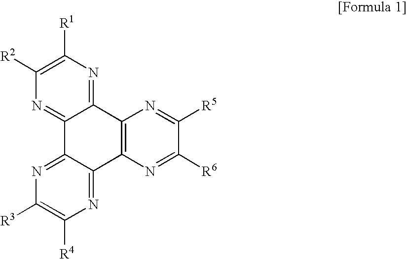
- Specific examples of the materials for forming the n-type organic material layer include the compound of the following formula 1, but not limited thereto:
- R 1 to R 6 are each independently selected from the group consisting of hydrogen, a halogen atom, nitrile (—CN), nitro (—NO 2 ), sulfonyl (—SO 2 R 11 ), sulfoxide (—SOR 11 ), sulfonamide (—SO 2 NR 11 R 12 ), sulfonate (—SO 3 R 11 ), trifluoromethyl (—CF 3 ), ester (—COOR 11 ), amide (—CONHR 11 or —CONR 11 R 12 ), substituted or unsubstituted linear or branched C 1 -C 12 alkoxy, substituted or unsubstituted linear or branched C 1 -C 12 alkyl, substituted or unsubstituted aromatic or non-aromatic heterocycle, substituted or unsubstituted aryl, substituted or unsubstituted mono-arylamine or di-arylamine, and substituted or unsubstituted aralkylamine
- R 11 and R 12 are selected from the group consisting of substituted or unsubstituted C 1 -C 60 alkyl, substituted or unsubstituted aryl, and substituted or unsubstituted 5- to 7-membered heterocycle.
- examples of the materials for forming the n-type organic material layer include 2,3,5,6-tetrafluoro-7,7,8,8-tetracyanoquinodimethane (F4TCNQ), fluorine-substituted 3,4,9,10-perylenetetracarboxylic dianhydride (PTCDA), cyano-substituted 3,4,9,10-perylenetetracarboxylic dianhydride (PTCDA), naphthalenetetracarboxylicdianhydride (NTCDA), fluorine-substituted naphthalenetetracarboxylicdianhydride (NTCDA), and cyano-substituted naphthalenetetracarboxylicdianhydride (NTCDA).
- F4TCNQ 2,3,5,6-tetrafluoro-7,7,8,8-tetracyanoquinodimethane
- PTCDA fluorine-substituted 3,4,9,10-per
- the p-type organic material layer to form an NP junction with the n-type organic material layer can serve as a hole injecting layer (HIL), a hole transporting layer (HTL) or a light emitting layer (EML).
- HIL hole injecting layer
- HTL hole transporting layer
- EML light emitting layer
- the holes formed in the NP junction of the n-type organic material layer and the p-type organic material layer can be transported to a light emitting region via the p-type hole injecting layer, the p-type hole transporting layer or the p-type light emitting layer.
- the HOMO energy level of the p-type hole injecting layer, the p-type hole transporting layer or the p-type light emitting layer has an energy level difference of about 1 eV or less from that of the LUMO energy level of the n-type organic material layer, for example, and preferably about 0.5 eV or less.
- the materials for forming the p-type organic material layer include an arylamine-based compound, a conductive polymer, and a block copolymer having both of conjugated and non-conjugated portions, but not limited thereto.
- At least two layers selected from the first conductive layer, the intermediate conductive layer and the second conductive layer by the NP junction can be formed of the same materials, and particularly the conductive layers can be formed of materials selected from Ca, Ca—Ag, Ag-IZO and Mg—Ag.
- the organic material layer to which the electrons are injected from the conductive layer with a cathode voltage being applied comprises a compound containing a functional group selected from an imidazole group, an oxazole group and a thiazole group, in order to prevent the reduction in electron injection characteristics due to contact between the cathode and organic material.
- the organic material layer to which the electrons are injected from the conductive layer with a cathode being applied can be an electron transporting layer.
- the method for improving the electron injection characteristics by formation of the organic material layer comprising the compound is effective for the cases wherein the stacked organic light emitting device according to the present invention has a reverse structure, in which the first conductive layer positioned on the substrate is a cathode electrode, and the second conductive layer positioned on the uppermost side is an anode electrode.
- the compound containing a functional group selected from an imidazole group, an oxazole group and a thiazole group include the compounds represented by the following formulae 2 or 3:
- R 7 and R 8 may be the same as or different from each other, and are each independently hydrogen, a C 1 -C 20 aliphatic hydrocarbon, or an aromatic ring or aromatic heterocycle;
- Ar is an aromatic ring or aromatic heterocycle;
- R 9 is hydrogen, a C 1 -C 6 aliphatic hydrocarbon, or an aromatic ring or aromatic heterocycle;
- X is O, S or NR 13 ;
- R 13 is hydrogen, a C 1 -C 7 aliphatic hydrocarbon, or an aromatic ring or aromatic heterocycle; provided that R 7 and R 8 are not hydrogen at the same time;
- R 10 and R 14 may be the same as or different from each other, and are each independently hydrogen, a C 1 -C 24 alkyl, a C 5 -C 20 aryl or heteroatom-containing substituted aryl, halogen or alkylene capable of forming a fused ring with a benzazole ring, or a heteroatom-containing alkylene;
- B as a linking unit, is alkylene, arylene, substituted alkylene, or substituted arylene to link the multiple benzazoles to be conjugated or non-conjugated; and n is an integer of 3 to 8.
- the first conductive layer can be formed of an anode material or a cathode material.
- the first conductive layer in the case where the first conductive layer is formed of the anode material, it can be formed of a metal, a metal oxide or a conductive polymer.
- the conductive polymer can comprise the electroconductive polymers.
- the first conductive layer preferably has a Fermi energy level of about 2.5 to 5.5 eV. It is preferable that an n-type organic material layer is formed on the first conductive layers to form an NP junction with the p-type organic material layer, so that the conductive layer may be formed of various conductive materials by lowering the energy barrier for injecting holes from the first conductive layer to the p-type organic material layer of the first light emitting unit.
- Non-limitative examples of the conductive materials include carbon, aluminum, calcium, vanadium, chromium, copper, zinc, silver, gold, other metals, and an alloy thereof; zinc oxide, indium oxide, tin oxide, indium tin oxide (ITO), indium zinc oxide (IZO) and other similar metal oxides, metal-metal oxide laminates such as Ca—Ag and Ca-IZO.
- the organic light emitting device is of a top emission type, opaque materials excellent in light reflection, as well as the transparent materials can be used for the first conductive layer.
- transparent materials should be used for the first conductive layer, and if opaque materials are used, a thin film which is substantially transparent should be formed.
- At least one intermediate conductive layer serves as a common electrode, which functions as an anode electrode, as well as a cathode electrode.
- the intermediate conductive layer can be in a stacked form comprising an intermediate cathode electrode layer and an intermediate anode electrode layer, or in a form comprising a single conductive layer. If the intermediate conductive layer is in the form of a single conductive layer, it is preferable that it is formed of transparent materials having a work function similar to that of the conventionally used cathode materials and a visible ray transmittance of 50% or more. If the opaque metal is used for the intermediate conductive layer, the thickness of the intermediate conductive layer should be sufficiently low such that it is substantially transparent.
- the intermediate conductive layer can be formed using Ca or Mg having a low work function, in this case, Ca, Ca—Ag, Ag-IZO or Ma—Ag is preferable.
- Ca-IZO is employed, the visible ray transmittance can be improved, and thus in the case of the stacked organic light emitting device, the luminance increases in proportion to the number of the units of the organic light emitting device stacked at a drive voltage. Accordingly, it is preferably used for the intermediate conductive layer in the organic light emitting device according to the present invention.
- the second conductive layer can be formed of an anode material or a cathode material.
- the second conductive layer is formed of the cathode material
- materials having low work functions are preferably used for the second conductive layer for promoting electron injection.
- the second conductive layer can be formed of, but not limited thereto, metal such s magnesium, calcium, sodium, potassium, titanium, indium, yttrium, lithium, gadolinium, aluminum, silver, tin and lead, or an alloy thereof; and multilayer structure materials such as LiF/Al and LiO/Al.
- the first conductive layer, the intermediate conductive layer and the second conductive layer can comprise the same organic materials or different organic materials, as described above.
- EML Light Emitting Layer
- Each light emitting unit of the stacked organic light emitting device comprises a light emitting layer.
- hole transportation and electron transportation are performed at the same time, and thus the light emitting layer has both of the n-type characteristics and the p-type characteristics.
- the light emitting layer in which electron transportation is faster than hole transportation can be defined as an n-type light emitting layer, and the light emitting layer in which hole transportation is faster than electron transportation can be defined as a p-type light emitting layer.
- the n-type light emitting layer Since in the n-type light emitting layer, electron transportation is faster than hole transportation, light emits around the interface between the hole transporting layer and the light emitting layer. Accordingly, if the LUMO level of the hole transporting layer is higher than the LUMO level of the light emitting layer, better light emitting efficiency can be obtained.
- the materials for the n-type light emitting layer include, but not limited thereto, aluminum tris(8-hydroxyquinoline) (Alq3); 8-hydroxyquinoline beryllium (BAlq); benzoxazole compounds, benzthiazole compounds or benzimidazole compounds; polyfluorene compounds; and silacyclopentadiene (silole) compounds.
- a light emitting unit having an NP junction structure between the n-type organic material layer and the p-type light emitting layer can be prepared without use of the hole injecting layer and the hole transporting layer.
- Materials for the p-type light emitting layer are not limited, but they include carbazole compounds; anthracene compounds; polyphenylenevinylene (PPV) polymers; and spiro compounds.
- ETL Electron Transporting Layer
- Each light emitting unit of the stacked organic light emitting device can comprise an electron transporting layer.
- materials for the electron transporting layer materials having a high electron mobility are preferable to receive electrons from the cathode to the light emitting layer.
- the materials for the electron transporting layer are not limited, but they include aluminum tris(8-hydroxyquinoline) (Alq3); Alq3 structure-containing organic compounds; hydroxyflavone-metal complex compounds; and silacyclopentadiene (silole) compounds.
- indium zinc oxide (IZO) was coated to a thicknesses of 1000 ⁇ by vacuum deposition using a sputtering deposition apparatus, and on the formed conductive layer, HAT having the following structure was coated to a thicknesses of 500 ⁇ by thermal vacuum deposition to form a transparent anode comprising the IZO and HAT n-type organic material layers.
- a Ca intermediate electrode was coated to a thicknesses of 250 ⁇ by thermal vacuum deposition
- HAT was coated to a thicknesses of about 500 ⁇ by thermal vacuum deposition
- NPB was coated to a thicknesses of about 400 ⁇ by deposition
- Alq3 was coated by deposition for the light emitting layer
- imidazole compound was coated by deposition for the electron transporting layer.
- a thin film of lithium fluoride (LiF) having a thickness of 15 ⁇ and aluminum having a thickness of 1000 ⁇ were coated by vacuum deposition to form a conductive layer.
- an organic light emitting device is completed by forming a pulse voltage regulator on the Ca layer as the intermediate conductive layer and a ground electric potential on the Al and IZO conductive layers.
- the deposition rate of the organic material was maintained at about 0.4 to 0.7 ⁇ /sec
- the deposition rate of LiF was maintained at about 0.3 ⁇ /sec
- the deposition rate of calcium and aluminum was maintained at about 2 ⁇ /sec.
- the degree of a vacuum in the deposition chamber upon deposition was maintained at about 2 ⁇ 10 ⁇ 7 to 5 ⁇ 10 ⁇ 8 torr.
- Table 1 shows luminances and color coordinates of the blue and green lights according to the forward and reverse voltages.
- FIG. 23 illustrates the light emission spectrum. Further, when reverse and forward voltages are applied using a pulse generator at 60 Hz, light in mixed color of blue and green colors was observed, and as shown in FIG. 24 and FIG. 25 , the color of the emitted light varied in blue to green depending on the width of the pulse or the pulse voltage.
- the light emission device for emitting two-color light according to the forward voltage and the reverse voltage can be obtained by preparing a device of a double stacked structure according to the present invention, and that a device having variance in the colors of the emitted light can be obtained by varying the width of the pulse or the intensity of the forward voltage and the reverse voltage.
Abstract
Description
E nL −E F≦4 eV (1)
E pH −E nL≦1 eV (2)
-
- 100, 200, 300, 400, 500, 600, 700, 800: Substrate
- 110, 210, 210 a, 210 b, 310, 410, 510, 610, 710, 810: First conductive layer
- 120, 220, 320, 420, 520, 620, 720, 820: Second conductive layer
- 311, 321, 411, 421, 431, 511, 621, 531, 611, 621, 631, 641, 711, 721, 731, 741, 811, 821, 831, 841: N-type organic material layer
- 112, 122, 212, 222, 232, 312, 322, 412, 422, 432, 512, 522, 532, 612, 622, 632, 642, 712, 722, 732, 742, 812, 822, 832, 842: Hole transporting layer
- 113, 123, 213, 223, 233, 313, 323, 413, 423, 433, 513, 523, 533, 613, 623, 633, 643, 713, 723, 733, 743, 813, 823, 833, 843: Light emitting layer
- 114, 124, 214, 224, 234, 314, 324, 414, 424, 434, 514, 524, 534, 614, 624, 634, 644, 714, 724, 734, 744, 814, 824, 834, 844: Electron transporting layer
- 130, 230, 240, 330, 430, 440, 530, 540, 630, 640, 650, 730, 740, 750, 830, 840, 850: Intermediate conductive layer
- 350, 450, 550, 650, 750, 850: Pulse generator
E nL −E F≦4 eV (1)
E pH −E nL≦1 eV (2)


| TABLE 1 |
| Luminances and color coordinates of the blue and green lights according to the |
| forward and reverse voltages |
| Forward voltage | Reverse voltage | |
| (Blue light emission) | (Green light emission) |
| Current | Color | Color | ||||
| density | Voltage | Luminance | coordinate | Voltage | Luminance | Coordinate |
| (mA/cm2) | (V) | (cd/m2) | (x, y) | (V) | (cd/m2) | (x, y) |
| 10 | 5.3 | 375 | 0.136, 0.167 | 3.7 | 333 | 0.371, 0.576 |
| 50 | 6.3 | 1772 | 0.136, 0.167 | 4.4 | 1731 | 0.371, 0.576 |
| 100 | 7.0 | 3496 | 0.136, 0.167 | 4.9 | 3547 | 0.371, 0.576 |
Claims (32)
E nL −E F≦4 eV (1)
E pH −E nL≦1 eV (2)


Applications Claiming Priority (3)
| Application Number | Priority Date | Filing Date | Title |
|---|---|---|---|
| KR10-2006-0005200 | 2006-01-18 | ||
| KR20060005200 | 2006-01-18 | ||
| PCT/KR2007/000277 WO2007083918A1 (en) | 2006-01-18 | 2007-01-17 | Oled having stacked organic light-emitting units |
Publications (2)
| Publication Number | Publication Date |
|---|---|
| US20090009101A1 US20090009101A1 (en) | 2009-01-08 |
| US8680693B2 true US8680693B2 (en) | 2014-03-25 |
Family
ID=38287827
Family Applications (1)
| Application Number | Title | Priority Date | Filing Date |
|---|---|---|---|
| US12/087,929 Active 2029-07-30 US8680693B2 (en) | 2006-01-18 | 2007-01-17 | OLED having stacked organic light-emitting units |
Country Status (7)
| Country | Link |
|---|---|
| US (1) | US8680693B2 (en) |
| EP (1) | EP1974590B1 (en) |
| JP (3) | JP2009524189A (en) |
| KR (1) | KR100845694B1 (en) |
| CN (1) | CN101371619B (en) |
| TW (1) | TWI371987B (en) |
| WO (1) | WO2007083918A1 (en) |
Cited By (9)
| Publication number | Priority date | Publication date | Assignee | Title |
|---|---|---|---|---|
| US20130153879A1 (en) * | 2010-08-17 | 2013-06-20 | Lg Chem, Ltd. | Organic light-emitting device |
| US20140252335A1 (en) * | 2012-08-14 | 2014-09-11 | Guardian Industries Corp. | Organic light emitting diode with transparent electrode and method of making same |
| US20150144895A1 (en) * | 2012-05-31 | 2015-05-28 | Lg Chem, Ltd. | Organic electroluminescent device |
| US9627641B2 (en) | 2010-09-24 | 2017-04-18 | Siemens Aktiengesellschaft | Charge carrier modulation for color and brightness coordination in organic light-emitting diodes |
| WO2019147479A1 (en) | 2018-01-25 | 2019-08-01 | OLEDWorks LLC | Method for mask-free oled deposition and manufacture |
| US10396296B2 (en) * | 2016-07-13 | 2019-08-27 | Samsung Display Co., Ltd. | Organic light-emitting device |
| US10516129B2 (en) | 2017-11-21 | 2019-12-24 | Boe Technology Group Co., Ltd. | OLED device, method for driving OLED device, OLED substrate, method for manufacturing OLED substrate and display device |
| US10840158B2 (en) | 2017-12-04 | 2020-11-17 | Au Optronics Corporation | Pixel structure |
| US10916567B2 (en) | 2008-07-10 | 2021-02-09 | Semiconductor Energy Laboratory Co., Ltd. | Light-emitting device and electronic device using the same |
Families Citing this family (85)
| Publication number | Priority date | Publication date | Assignee | Title |
|---|---|---|---|---|
| US7560175B2 (en) * | 1999-12-31 | 2009-07-14 | Lg Chem, Ltd. | Electroluminescent devices with low work function anode |
| KR100721656B1 (en) * | 2005-11-01 | 2007-05-23 | 주식회사 엘지화학 | Organic electronic devices |
| KR100377321B1 (en) * | 1999-12-31 | 2003-03-26 | 주식회사 엘지화학 | Electronic device comprising organic compound having p-type semiconducting characteristics |
| KR100845694B1 (en) | 2006-01-18 | 2008-07-11 | 주식회사 엘지화학 | Oled having stacked organic light-emitting units |
| KR101384785B1 (en) * | 2006-06-01 | 2014-04-14 | 가부시키가이샤 한도오따이 에네루기 켄큐쇼 | Light-emitting element, light-emitting device and an electronic device |
| US9397308B2 (en) * | 2006-12-04 | 2016-07-19 | Semiconductor Energy Laboratory Co., Ltd. | Light emitting element, light emitting device, and electronic device |
| EP2031036B1 (en) | 2007-08-31 | 2012-06-27 | Semiconductor Energy Laboratory Co., Ltd. | Light-emitting element, light-emitting device, and electronic appliance |
| KR101407579B1 (en) * | 2007-09-17 | 2014-06-13 | 삼성디스플레이 주식회사 | Organic light emitting device and method of driving the same |
| US20090091242A1 (en) * | 2007-10-05 | 2009-04-09 | Liang-Sheng Liao | Hole-injecting layer in oleds |
| KR101434360B1 (en) * | 2007-10-08 | 2014-08-26 | 삼성디스플레이 주식회사 | White organic light emitting display |
| KR101420427B1 (en) * | 2007-10-09 | 2014-07-16 | 엘지디스플레이 주식회사 | Oled |
| EP2068380B1 (en) | 2007-10-15 | 2011-08-17 | Novaled AG | Organic electroluminescent component |
| KR101434363B1 (en) * | 2007-11-07 | 2014-08-26 | 삼성디스플레이 주식회사 | White Organic light emitting device |
| US8629865B2 (en) * | 2007-12-14 | 2014-01-14 | Koninklijke Philips N.V. | Organic light-emitting device with adjustable charge carrier injection |
| WO2009139607A2 (en) * | 2008-05-16 | 2009-11-19 | 주식회사 엘지화학 | Stacked organic light-emitting diode |
| JP5460107B2 (en) * | 2008-06-20 | 2014-04-02 | キヤノン株式会社 | Laminated organic light emitting device and image display apparatus or digital camera having the same |
| US20110121738A1 (en) * | 2008-06-20 | 2011-05-26 | Canon Kabushiki Kaisha | Light-emitting apparatus |
| JP5478954B2 (en) * | 2008-07-11 | 2014-04-23 | キヤノン株式会社 | Organic electroluminescence display device |
| EP2427925B1 (en) | 2009-05-05 | 2017-12-20 | Koninklijke Philips N.V. | Electroluminescent device |
| JP5273381B2 (en) * | 2009-05-12 | 2013-08-28 | 株式会社ジャパンディスプレイ | Organic EL element and organic EL display device |
| DE102009034822A1 (en) * | 2009-07-27 | 2011-02-03 | Osram Opto Semiconductors Gmbh | Electronic component as well as electrical contact |
| US20110248244A1 (en) * | 2009-10-05 | 2011-10-13 | Emagin Corporation | Independently controlled stacked inverted organic light emitting diodes and a method of manufacturing same |
| KR20110045569A (en) * | 2009-10-27 | 2011-05-04 | 한국전자통신연구원 | Stacked organic light emitting device |
| KR101874448B1 (en) * | 2011-05-09 | 2018-07-06 | 삼성디스플레이 주식회사 | Organic light emitting display device |
| US9818901B2 (en) * | 2011-05-13 | 2017-11-14 | International Business Machines Corporation | Wafer bonded solar cells and fabrication methods |
| JP6070567B2 (en) * | 2011-11-17 | 2017-02-01 | コニカミノルタ株式会社 | Transparent electrode and electronic device |
| KR20130062107A (en) | 2011-12-02 | 2013-06-12 | 삼성전자주식회사 | Textile orgainc light emitting device and method of manufacturing the same |
| CN102655219A (en) * | 2012-02-23 | 2012-09-05 | 京东方科技集团股份有限公司 | Multicolour OLED (organic light-emitting diode), multicolour OLED unit and display device |
| KR101433524B1 (en) * | 2012-05-25 | 2014-08-22 | 주식회사 엘지화학 | Organic light emitting device and method for manufacturing the same |
| KR101539842B1 (en) * | 2012-05-31 | 2015-07-28 | 주식회사 엘지화학 | Organic light emitting device |
| US9269919B2 (en) * | 2012-05-31 | 2016-02-23 | Lg Chem, Ltd. | Stacked organic light emitting diode |
| JP6305997B2 (en) * | 2012-06-19 | 2018-04-04 | コーニンクレッカ フィリップス エヌ ヴェKoninklijke Philips N.V. | Organic electroluminescence device |
| DE102012211869A1 (en) * | 2012-07-06 | 2014-01-09 | Osram Opto Semiconductors Gmbh | Organic light emitting device |
| JP2015215940A (en) | 2012-08-17 | 2015-12-03 | 出光興産株式会社 | Light-emitting device, electronic device, and method for manufacturing light-emitting device |
| GB2505499B (en) * | 2012-09-03 | 2017-03-08 | Dst Innovations Ltd | Electroluminescent displays and lighting |
| JP6384326B2 (en) | 2012-10-31 | 2018-09-05 | コニカミノルタ株式会社 | Organic electroluminescence device |
| JP6225915B2 (en) * | 2012-11-09 | 2017-11-08 | コニカミノルタ株式会社 | Organic electroluminescence device |
| KR102040872B1 (en) * | 2012-12-13 | 2019-11-06 | 삼성디스플레이 주식회사 | Organic Light Emitting Diode, Organic Light Emitting Display Device, and method for controlling dual emission of OLED |
| CN104813488B (en) * | 2013-01-05 | 2019-02-22 | 深圳云英谷科技有限公司 | Show equipment and the method for manufacturing and driving the display equipment |
| TWI614928B (en) * | 2013-06-07 | 2018-02-11 | 樂金顯示科技股份有限公司 | Organic light emitting device |
| US10033007B2 (en) | 2013-06-07 | 2018-07-24 | Lg Display Co., Ltd. | Organic light emitting diode |
| DE102013107225A1 (en) * | 2013-07-09 | 2015-01-15 | Osram Oled Gmbh | Optoelectronic component arrangement, method for producing an optoelectronic component arrangement, method for operating an optoelectronic component arrangement |
| DE102013110483A1 (en) * | 2013-09-23 | 2015-03-26 | Osram Oled Gmbh | Optoelectronic component device and method for operating an optoelectronic component |
| KR101820038B1 (en) * | 2013-09-30 | 2018-02-28 | 엘지디스플레이 주식회사 | Transparent electrode and organic electronic device comprising the same |
| US9142595B2 (en) * | 2013-10-18 | 2015-09-22 | OLEDWorks LLC | Color-tunable OLED lighting device |
| KR101944483B1 (en) | 2013-12-26 | 2019-01-31 | 엘지디스플레이 주식회사 | Organic light emitting device |
| KR102165234B1 (en) * | 2014-04-25 | 2020-10-14 | 엘지디스플레이 주식회사 | White organic light emitting device |
| CN103996792B (en) * | 2014-04-30 | 2016-04-27 | 京东方科技集团股份有限公司 | Organic luminescent device and manufacture method and organic light-emitting display device and driving method |
| KR101707326B1 (en) | 2014-09-15 | 2017-02-16 | 주식회사 엘지화학 | Organic light emitting device |
| CN104538553B (en) * | 2014-12-31 | 2017-08-04 | 北京维信诺科技有限公司 | A kind of organic electroluminescence device of Color tunable |
| WO2017031265A1 (en) * | 2015-08-18 | 2017-02-23 | Wake Forest University | Frequency dependent light emitting devices |
| KR102406606B1 (en) * | 2015-10-08 | 2022-06-09 | 삼성디스플레이 주식회사 | Organic light emitting device, organic light emitting display device having the same and fabricating method of the same |
| KR101999709B1 (en) | 2016-03-21 | 2019-07-12 | 주식회사 엘지화학 | Organic light emitting device |
| US20170352709A1 (en) * | 2016-06-03 | 2017-12-07 | Universal Display Corporation | Architecture for very high resolution amoled display |
| JP6884534B2 (en) * | 2016-09-15 | 2021-06-09 | 株式会社東芝 | Printhead and image forming device |
| CN109564931B (en) * | 2017-04-12 | 2023-04-04 | 京东方科技集团股份有限公司 | Stacked organic light emitting device, organic light emitting diode display device, and method of manufacturing stacked organic light emitting device |
| CN107134256A (en) * | 2017-05-03 | 2017-09-05 | 京东方科技集团股份有限公司 | Display panel and its driving method, display device |
| CN107104128B (en) * | 2017-05-11 | 2021-04-27 | 京东方科技集团股份有限公司 | Pixel unit, driving method, display panel and display device |
| CN107170779A (en) * | 2017-05-12 | 2017-09-15 | 京东方科技集团股份有限公司 | A kind of oled display substrate and display device |
| CN107420749B (en) * | 2017-07-25 | 2020-06-02 | 江苏集萃有机光电技术研究所有限公司 | Light emitting device capable of adjusting color temperature and color rendering index, adjusting method and lamp |
| CN107425129B (en) * | 2017-07-26 | 2019-12-06 | 上海天马有机发光显示技术有限公司 | organic light-emitting display panel, color temperature adjusting method thereof and display device |
| US11527519B2 (en) | 2017-11-27 | 2022-12-13 | Seoul Viosys Co., Ltd. | LED unit for display and display apparatus having the same |
| US11282981B2 (en) | 2017-11-27 | 2022-03-22 | Seoul Viosys Co., Ltd. | Passivation covered light emitting unit stack |
| US10892297B2 (en) | 2017-11-27 | 2021-01-12 | Seoul Viosys Co., Ltd. | Light emitting diode (LED) stack for a display |
| US10892296B2 (en) | 2017-11-27 | 2021-01-12 | Seoul Viosys Co., Ltd. | Light emitting device having commonly connected LED sub-units |
| US10748881B2 (en) | 2017-12-05 | 2020-08-18 | Seoul Viosys Co., Ltd. | Light emitting device with LED stack for display and display apparatus having the same |
| US10886327B2 (en) | 2017-12-14 | 2021-01-05 | Seoul Viosys Co., Ltd. | Light emitting stacked structure and display device having the same |
| US11552057B2 (en) | 2017-12-20 | 2023-01-10 | Seoul Viosys Co., Ltd. | LED unit for display and display apparatus having the same |
| US11522006B2 (en) | 2017-12-21 | 2022-12-06 | Seoul Viosys Co., Ltd. | Light emitting stacked structure and display device having the same |
| US11552061B2 (en) | 2017-12-22 | 2023-01-10 | Seoul Viosys Co., Ltd. | Light emitting device with LED stack for display and display apparatus having the same |
| CN108183174B (en) * | 2017-12-27 | 2020-05-12 | 武汉华美晨曦光电有限责任公司 | Alternating current driving white light OLED device with quantum well structure |
| US11114499B2 (en) | 2018-01-02 | 2021-09-07 | Seoul Viosys Co., Ltd. | Display device having light emitting stacked structure |
| US10784240B2 (en) | 2018-01-03 | 2020-09-22 | Seoul Viosys Co., Ltd. | Light emitting device with LED stack for display and display apparatus having the same |
| US20200028084A1 (en) | 2018-07-19 | 2020-01-23 | Lg Display Co., Ltd. | Organic electroluminescent device |
| KR102260883B1 (en) * | 2018-07-19 | 2021-06-07 | 엘지디스플레이 주식회사 | Organic electroluminescent device |
| CN109599420B (en) * | 2018-10-23 | 2021-02-26 | 武汉华星光电半导体显示技术有限公司 | Display panel and manufacturing method thereof |
| KR102520022B1 (en) * | 2018-11-26 | 2023-04-10 | 엘지디스플레이 주식회사 | Display device |
| CN109920928A (en) * | 2019-02-26 | 2019-06-21 | 武汉华星光电半导体显示技术有限公司 | Display panel and display device |
| CN110808338A (en) * | 2019-10-10 | 2020-02-18 | 复旦大学 | Tandem quantum dot device with double light emitting surfaces |
| CN111554819B (en) * | 2020-04-27 | 2023-06-23 | 南方科技大学 | Light-emitting device, light-emitting color adjusting method thereof and display device |
| WO2022024239A1 (en) * | 2020-07-29 | 2022-02-03 | シャープ株式会社 | Light emitting element and driving method for light emitting element |
| CN111968565B (en) * | 2020-08-11 | 2021-08-03 | Tcl华星光电技术有限公司 | Self-luminous pixel circuit and display panel |
| CN112164753B (en) * | 2020-09-28 | 2022-01-11 | 京东方科技集团股份有限公司 | OLED device and preparation method thereof, display substrate and display device |
| CN112700748B (en) * | 2020-12-28 | 2021-11-26 | 合肥视涯显示科技有限公司 | Display panel, control method thereof and display device |
| CN112909053A (en) * | 2021-01-26 | 2021-06-04 | 京东方科技集团股份有限公司 | Display device, display panel and manufacturing method thereof |
Citations (196)
| Publication number | Priority date | Publication date | Assignee | Title |
|---|---|---|---|---|
| US3180730A (en) | 1959-04-09 | 1965-04-27 | Azoplate Corp | Material for electrophotographic purposes |
| US3567450A (en) | 1968-02-20 | 1971-03-02 | Eastman Kodak Co | Photoconductive elements containing substituted triarylamine photoconductors |
| US3658520A (en) | 1968-02-20 | 1972-04-25 | Eastman Kodak Co | Photoconductive elements containing as photoconductors triarylamines substituted by active hydrogen-containing groups |
| US4356429A (en) | 1980-07-17 | 1982-10-26 | Eastman Kodak Company | Organic electroluminescent cell |
| US4359507A (en) | 1981-11-19 | 1982-11-16 | Atlantic Richfield Company | Mixed ethylene and propylene carbonate-containing organic polyisocyanate adhesive binder composition |
| US4720432A (en) | 1987-02-11 | 1988-01-19 | Eastman Kodak Company | Electroluminescent device with organic luminescent medium |
| US4769292A (en) | 1987-03-02 | 1988-09-06 | Eastman Kodak Company | Electroluminescent device with modified thin film luminescent zone |
| US4780536A (en) | 1986-09-05 | 1988-10-25 | The Ohio State University Research Foundation | Hexaazatriphenylene hexanitrile and its derivatives and their preparations |
| US4885211A (en) | 1987-02-11 | 1989-12-05 | Eastman Kodak Company | Electroluminescent device with improved cathode |
| US4885221A (en) | 1986-12-06 | 1989-12-05 | Kabushiki Kaisha Toshiba | Electrophotography apparatus and electrophtographic process for developing positive image from positive or negative film |
| US5059862A (en) | 1990-07-26 | 1991-10-22 | Eastman Kodak Company | Electroluminescent device with improved cathode |
| US5059861A (en) | 1990-07-26 | 1991-10-22 | Eastman Kodak Company | Organic electroluminescent device with stabilizing cathode capping layer |
| US5061569A (en) | 1990-07-26 | 1991-10-29 | Eastman Kodak Company | Electroluminescent device with organic electroluminescent medium |
| US5121029A (en) | 1987-12-11 | 1992-06-09 | Idemitsu Kosan Co., Ltd. | Electroluminescence device having an organic electroluminescent element |
| US5141671A (en) | 1991-08-01 | 1992-08-25 | Eastman Kodak Company | Mixed ligand 8-quinolinolato aluminum chelate luminophors |
| US5150006A (en) | 1991-08-01 | 1992-09-22 | Eastman Kodak Company | Blue emitting internal junction organic electroluminescent device (II) |
| US5151629A (en) | 1991-08-01 | 1992-09-29 | Eastman Kodak Company | Blue emitting internal junction organic electroluminescent device (I) |
| US5247190A (en) | 1989-04-20 | 1993-09-21 | Cambridge Research And Innovation Limited | Electroluminescent devices |
| US5276380A (en) | 1991-12-30 | 1994-01-04 | Eastman Kodak Company | Organic electroluminescent image display device |
| US5283182A (en) | 1986-09-17 | 1994-02-01 | Beecham Group Plc | Preparation of immobilized hydantoinase stabilized with divalent metal ions |
| US5294810A (en) | 1989-03-31 | 1994-03-15 | Kabushiki Kaisha Toshiba | Organic electroluminescent device |
| US5294870A (en) | 1991-12-30 | 1994-03-15 | Eastman Kodak Company | Organic electroluminescent multicolor image display device |
| US5366811A (en) | 1990-09-20 | 1994-11-22 | Idemitsu Kosan Co., Ltd. | Organic electroluminescence device |
| US5405709A (en) | 1993-09-13 | 1995-04-11 | Eastman Kodak Company | White light emitting internal junction organic electroluminescent device |
| US5457565A (en) | 1992-11-19 | 1995-10-10 | Pioneer Electronic Corporation | Organic electroluminescent device |
| US5484922A (en) | 1992-07-13 | 1996-01-16 | Eastman Kodak Company | Internal junction organic electroluminescent device with a novel composition |
| US5503910A (en) | 1994-03-29 | 1996-04-02 | Idemitsu Kosan Co., Ltd. | Organic electroluminescence device |
| US5540999A (en) | 1993-09-09 | 1996-07-30 | Takakazu Yamamoto | EL element using polythiophene |
| US5593788A (en) | 1996-04-25 | 1997-01-14 | Eastman Kodak Company | Organic electroluminescent devices with high operational stability |
| US5608287A (en) | 1995-02-23 | 1997-03-04 | Eastman Kodak Company | Conductive electron injector for light-emitting diodes |
| US5616427A (en) | 1995-06-05 | 1997-04-01 | Nec Corporation | Organic thin film EL device having long lifetime |
| US5645948A (en) | 1996-08-20 | 1997-07-08 | Eastman Kodak Company | Blue organic electroluminescent devices |
| EP0797375A2 (en) | 1996-03-19 | 1997-09-24 | Motorola, Inc. | Organic electroluminescent device with new hole transporting materials |
| US5677572A (en) | 1996-07-29 | 1997-10-14 | Eastman Kodak Company | Bilayer electrode on a n-type semiconductor |
| US5683823A (en) | 1996-01-26 | 1997-11-04 | Eastman Kodak Company | White light-emitting organic electroluminescent devices |
| US5688551A (en) | 1995-11-13 | 1997-11-18 | Eastman Kodak Company | Method of forming an organic electroluminescent display panel |
| US5703436A (en) * | 1994-12-13 | 1997-12-30 | The Trustees Of Princeton University | Transparent contacts for organic devices |
| US5714838A (en) | 1996-09-20 | 1998-02-03 | International Business Machines Corporation | Optically transparent diffusion barrier and top electrode in organic light emitting diode structures |
| US5739545A (en) | 1997-02-04 | 1998-04-14 | International Business Machines Corporation | Organic light emitting diodes having transparent cathode structures |
| US5757139A (en) * | 1997-02-03 | 1998-05-26 | The Trustees Of Princeton University | Driving circuit for stacked organic light emitting devices |
| US5755999A (en) | 1997-05-16 | 1998-05-26 | Eastman Kodak Company | Blue luminescent materials for organic electroluminescent devices |
| US5766779A (en) | 1996-08-20 | 1998-06-16 | Eastman Kodak Company | Electron transporting materials for organic electroluminescent devices |
| US5776623A (en) | 1996-07-29 | 1998-07-07 | Eastman Kodak Company | Transparent electron-injecting electrode for use in an electroluminescent device |
| US5776622A (en) | 1996-07-29 | 1998-07-07 | Eastman Kodak Company | Bilayer eletron-injeting electrode for use in an electroluminescent device |
| US5792568A (en) | 1995-04-25 | 1998-08-11 | Sharp Kabushiki Kaisha | Organic electroluminescent element |
| US5811833A (en) | 1996-12-23 | 1998-09-22 | University Of So. Ca | Electron transporting and light emitting layers based on organic free radicals |
| WO1998049163A1 (en) | 1997-04-25 | 1998-11-05 | Akzo Nobel N.V. | Complex comprising a rare-earth metal ion and a complexing moiety |
| US5837391A (en) | 1996-01-17 | 1998-11-17 | Nec Corporation | Organic electroluminescent element having electrode between two fluorescent media for injecting carrier thereinto |
| US5840217A (en) | 1994-04-07 | 1998-11-24 | Hoechst Aktiengesellschaft | Spiro compounds and their use as electroluminescence materials |
| US5851709A (en) | 1997-10-31 | 1998-12-22 | Eastman Kodak Company | Method for selective transfer of a color organic layer |
| US5917280A (en) * | 1997-02-03 | 1999-06-29 | The Trustees Of Princeton University | Stacked organic light emitting devices |
| US5917279A (en) | 1995-11-20 | 1999-06-29 | Bayer Aktiengesllschaft | Intermediate layer in electroluminescent arrangements containing finely divided inorganic particles |
| US5927247A (en) | 1996-09-26 | 1999-07-27 | Sanshin Kogyo Kabushiki Kaisha | Direct injected engine |
| US5928802A (en) | 1997-05-16 | 1999-07-27 | Eastman Kodak Company | Efficient blue organic electroluminescent devices |
| US5932362A (en) | 1995-03-08 | 1999-08-03 | Ricoh Company, Ltd. | Organic electroluminescent element |
| WO1999039393A1 (en) | 1998-02-02 | 1999-08-05 | International Business Machines Corporation | Anode modification for organic light emitting diodes |
| US5935721A (en) | 1998-03-20 | 1999-08-10 | Eastman Kodak Company | Organic electroluminescent elements for stable electroluminescent |
| US5935720A (en) | 1997-04-07 | 1999-08-10 | Eastman Kodak Company | Red organic electroluminescent devices |
| US5969474A (en) | 1996-10-24 | 1999-10-19 | Tdk Corporation | Organic light-emitting device with light transmissive anode and light transmissive cathode including zinc-doped indium oxide |
| US5982345A (en) * | 1996-02-09 | 1999-11-09 | Tdk Corporation | Organic electroluminescent image display device |
| US5981306A (en) | 1997-09-12 | 1999-11-09 | The Trustees Of Princeton University | Method for depositing indium tin oxide layers in organic light emitting devices |
| US5998803A (en) | 1997-05-29 | 1999-12-07 | The Trustees Of Princeton University | Organic light emitting device containing a hole injection enhancement layer |
| US6020078A (en) | 1998-12-18 | 2000-02-01 | Eastman Kodak Company | Green organic electroluminescent devices |
| US6046543A (en) | 1996-12-23 | 2000-04-04 | The Trustees Of Princeton University | High reliability, high efficiency, integratable organic light emitting devices and methods of producing same |
| US6066357A (en) | 1998-12-21 | 2000-05-23 | Eastman Kodak Company | Methods of making a full-color organic light-emitting display |
| EP0732868B1 (en) | 1995-03-13 | 2000-05-24 | Pioneer Electronic Corporation | Organic electroluminescent display panel and method for manufacturing the same |
| US6097147A (en) | 1998-09-14 | 2000-08-01 | The Trustees Of Princeton University | Structure for high efficiency electroluminescent device |
| US6099750A (en) | 1995-11-23 | 2000-08-08 | Siemens Aktiengesellschaft | Use of organic compounds in the plastic columnar discotic liquid-crystal phase for transport of electric charges |
| JP2000223276A (en) | 1999-02-02 | 2000-08-11 | Idemitsu Kosan Co Ltd | Organic electroluminescent element and its manufacture |
| EP1029909A1 (en) | 1998-09-09 | 2000-08-23 | Idemitsu Kosan Co., Ltd. | Organic electroluminescence device and phenylenediamine derivative |
| US6137223A (en) | 1998-07-28 | 2000-10-24 | Eastman Kodak Company | Electron-injecting layer formed from a dopant layer for organic light-emitting structure |
| US6140763A (en) | 1998-07-28 | 2000-10-31 | Eastman Kodak Company | Interfacial electron-injecting layer formed from a doped cathode for organic light-emitting structure |
| US6171715B1 (en) | 1997-08-07 | 2001-01-09 | Fuji Photo Film Co., Ltd. | Organic electroluminescent element |
| US6172459B1 (en) | 1998-07-28 | 2001-01-09 | Eastman Kodak Company | Electron-injecting layer providing a modified interface between an organic light-emitting structure and a cathode buffer layer |
| WO2001006576A1 (en) | 1999-07-19 | 2001-01-25 | Uniax Corporation | Long-lifetime polymer light-emitting devices with improved luminous efficiency and radiance |
| US6188175B1 (en) * | 1995-04-18 | 2001-02-13 | Cambridge Display Technology Limited | Electroluminescent device |
| EP1076368A2 (en) | 1999-08-11 | 2001-02-14 | Eastman Kodak Company | A surface-emitting organic light-emitting diode |
| US6208075B1 (en) | 1998-11-05 | 2001-03-27 | Eastman Kodak Company | Conductive fluorocarbon polymer and method of making same |
| JP2001110571A (en) | 1999-07-30 | 2001-04-20 | Sony Corp | Organic field light emitting element |
| US6226890B1 (en) | 2000-04-07 | 2001-05-08 | Eastman Kodak Company | Desiccation of moisture-sensitive electronic devices |
| EP1099744A2 (en) | 1999-11-12 | 2001-05-16 | Canon Kabushiki Kaisha | Organic electroluminescent device |
| US6237529B1 (en) | 2000-03-03 | 2001-05-29 | Eastman Kodak Company | Source for thermal physical vapor deposition of organic electroluminescent layers |
| WO2001049806A1 (en) | 1999-12-31 | 2001-07-12 | Lg Chemical Co., Ltd | Electronic device comprising organic compound having p-type semiconducting characteristics |
| US6278236B1 (en) | 1999-09-02 | 2001-08-21 | Eastman Kodak Company | Organic electroluminescent devices with electron-injecting layer having aluminum and alkali halide |
| US6284393B1 (en) | 1996-11-29 | 2001-09-04 | Idemitsu Kosan Co., Ltd. | Organic electroluminescent device |
| US6312838B1 (en) | 1998-05-18 | 2001-11-06 | Sony Corporation | Organic electroluminescent device |
| US6320322B1 (en) * | 1998-12-24 | 2001-11-20 | Rohm Co., Ltd. | Light emitting appliance |
| US20020011782A1 (en) | 1999-01-21 | 2002-01-31 | Shuit-Tong Lee | Organic electroluminescent device with improved hole injecting structure |
| EP1179862A2 (en) | 2000-08-11 | 2002-02-13 | EASTMAN KODAK COMPANY (a New Jersey corporation) | Improved cathode layer in organic light-emitting diode devices |
| US20020025419A1 (en) | 1999-06-08 | 2002-02-28 | City University Of Hong Kong | White and colored organic electroluminescent devices using single emitting material by novel color change technique |
| US6352777B1 (en) | 1998-08-19 | 2002-03-05 | The Trustees Of Princeton University | Organic photosensitive optoelectronic devices with transparent electrodes |
| US20020048687A1 (en) | 2000-03-29 | 2002-04-25 | Idemitsu Kosan Co., Ltd. | Anthracene derivative and organic electroluminescence device using the derivative |
| US6404126B1 (en) | 1998-11-25 | 2002-06-11 | Tdk Corporation | Organic electroluminescent device having a conjugated polymer and an inorganic insulative electron injecting and transporting layer |
| US6413656B1 (en) | 1998-09-14 | 2002-07-02 | The University Of Southern California | Reduced symmetry porphyrin molecules for producing enhanced luminosity from phosphorescent organic light emitting devices |
| US20020084993A1 (en) * | 1998-09-02 | 2002-07-04 | Mototaka Taneya | Organic el emission device and method of driving the same |
| US6423429B2 (en) | 1998-03-02 | 2002-07-23 | Junji Kido | Organic electroluminescent devices |
| US20020100906A1 (en) | 2000-11-29 | 2002-08-01 | Takao Takiguchi | Metal coordination compound, luminescence device and display apparatus |
| US20020117962A1 (en) | 1998-02-02 | 2002-08-29 | Tilman A. Beierlein | Anode modification for organic light emitting diodes |
| US20020117662A1 (en) | 2000-12-25 | 2002-08-29 | Fuji Photo Film Co., Ltd. | Novel indole derivative, material for light-emitting device and light-emitting device using the same |
| JP2002246184A (en) | 2001-02-14 | 2002-08-30 | Fuji Photo Film Co Ltd | Light-emitting element |
| US20020121638A1 (en) | 2000-06-30 | 2002-09-05 | Vladimir Grushin | Electroluminescent iridium compounds with fluorinated phenylpyridines, phenylpyrimidines, and phenylquinolines and devices made with such compounds |
| US20020127427A1 (en) | 2001-01-02 | 2002-09-12 | Eastman Kodak Company | Organic light emitting diode devices with improved luminance efficiency |
| US6451455B1 (en) | 1998-04-01 | 2002-09-17 | The Trustees Of Princeton University | Metal complexes bearing both electron transporting and hole transporting moieties |
| US6451415B1 (en) | 1998-08-19 | 2002-09-17 | The Trustees Of Princeton University | Organic photosensitive optoelectronic device with an exciton blocking layer |
| US6458475B1 (en) | 1999-11-24 | 2002-10-01 | The Trustee Of Princeton University | Organic light emitting diode having a blue phosphorescent molecule as an emitter |
| US6465115B2 (en) | 1998-12-09 | 2002-10-15 | Eastman Kodak Company | Electroluminescent device with anthracene derivatives hole transport layer |
| US6475648B1 (en) | 2000-06-08 | 2002-11-05 | Eastman Kodak Company | Organic electroluminescent devices with improved stability and efficiency |
| US20020186214A1 (en) | 2001-06-05 | 2002-12-12 | Eastman Kodak Company | Method for saving power in an organic electroluminescent display using white light emitting elements |
| US6497969B2 (en) | 1997-09-05 | 2002-12-24 | Nessdisplay Co., Ltd. | Electroluminescent device having an organic layer including polyimide |
| US20020197511A1 (en) | 2001-05-16 | 2002-12-26 | D'andrade Brian | High efficiency multi-color electro-phosphorescent OLEDS |
| JP2003501795A (en) | 1999-06-09 | 2003-01-14 | ケンブリッジ、ディスプレイ、テクノロジー、リミテッド | Light emitting device |
| US20030012890A1 (en) | 1997-09-17 | 2003-01-16 | Thomas Weber | Method for producing a plasma by microwave irradiation |
| US20030017361A1 (en) | 1998-09-14 | 2003-01-23 | Thompson Mark E. | Organometallic complexes as phosphorescent emitters in organic LEDs |
| US6515298B2 (en) | 1999-07-21 | 2003-02-04 | The Trustees Of Princeton University | Intersystem crossing agents for efficient utilization of excitons in organic light emitting devices |
| WO2003012890A2 (en) | 2001-07-20 | 2003-02-13 | Novaled Gmbh | Light emitting component with organic layers |
| US20030040627A1 (en) | 2001-06-15 | 2003-02-27 | Hiroyuki Fujii | Luminescent organometallic compound and light emitting device |
| JP2003059667A (en) | 2001-06-04 | 2003-02-28 | Sanyo Electric Co Ltd | Organic electroluminescence element, luminous material and organic compound |
| JP2003073388A (en) | 2001-06-19 | 2003-03-12 | Canon Inc | Metal coordination compound and organic luminescent element |
| JP2003073665A (en) | 2001-09-03 | 2003-03-12 | Sanyo Electric Co Ltd | Material for light-emitting element |
| JP2003073387A (en) | 2001-09-04 | 2003-03-12 | Canon Inc | Metal coordination compound and organic luminescent element |
| US6534199B1 (en) | 1999-09-21 | 2003-03-18 | Idemitsu Kosan Co., Ltd. | Organic electroluminescence device and organic light emitting medium |
| US20030054198A1 (en) | 2000-12-01 | 2003-03-20 | Akira Tsuboyama | Metal coordination compound, luminescence device and display apparatus |
| US20030059646A1 (en) | 2000-11-30 | 2003-03-27 | Canon Kabushiki Kaisha | Luminescence device and display apparatus |
| US20030068528A1 (en) | 2001-08-29 | 2003-04-10 | Thompson Mark E. | Organic light emitting devices having carrier blocking layers comprising metal complexes |
| US20030068526A1 (en) | 2000-11-30 | 2003-04-10 | Canon Kabushiki Kaisha | Luminescence device and display apparatus |
| US20030068535A1 (en) | 2001-03-08 | 2003-04-10 | Takao Takiguchi | Metal coordination compound, luminescence device and display apparatus |
| US20030072966A1 (en) | 1998-12-28 | 2003-04-17 | Idemitsu Kosan Co., Ltd. | Organic electrolumescence device |
| US20030072964A1 (en) | 2001-10-17 | 2003-04-17 | Kwong Raymond C. | Phosphorescent compounds and devices comprising the same |
| US6566806B1 (en) * | 1999-11-08 | 2003-05-20 | Canon Kabushiki Kaisha | Luminescence device, and image-reading apparatus, data-processing apparatus and display apparatus including the device |
| JP2003146951A (en) | 2001-08-06 | 2003-05-21 | Mitsubishi Chemicals Corp | Anthracene-based compound, method for producing the same and organic electroluminescent element |
| US6573651B2 (en) | 2000-12-18 | 2003-06-03 | The Trustees Of Princeton University | Highly efficient OLEDs using doped ambipolar conductive molecular organic thin films |
| US20030124381A1 (en) | 2001-12-28 | 2003-07-03 | Thompson Mark E. | White light emitting OLEDs from combined monomer and aggregate emission |
| WO2003060956A2 (en) | 2002-01-18 | 2003-07-24 | Lg Chem, Ltd. | New material for transporting electrons and organic electroluminescent display using the same |
| US20030141809A1 (en) | 2001-06-15 | 2003-07-31 | Manabu Furugori | Organic electroluminescent device |
| US6602969B2 (en) | 2000-01-12 | 2003-08-05 | Sumitomo Chemical Company, Limited | Polymeric fluorescent substance and polymer light-emitting device |
| US20030151356A1 (en) | 1996-05-03 | 2003-08-14 | Karl Pichler | Organic light-emitting device and method of fabricating the same |
| US20030159729A1 (en) | 2000-04-27 | 2003-08-28 | Sean Shaheen | Photovoltaic cell |
| US20030170491A1 (en) * | 2002-02-15 | 2003-09-11 | Eastman Kodak Company | Providing an organic electroluminescent device having stacked electroluminescent units |
| US6627333B2 (en) | 2001-08-15 | 2003-09-30 | Eastman Kodak Company | White organic light-emitting devices with improved efficiency |
| WO2003083958A2 (en) | 2002-03-28 | 2003-10-09 | Novaled Gmbh | Transparent, thermally stable light-emitting component comprising organic layers |
| US20030189401A1 (en) * | 2002-03-26 | 2003-10-09 | International Manufacturing And Engineering Services Co., Ltd. | Organic electroluminescent device |
| US20030197465A1 (en) | 2002-04-03 | 2003-10-23 | Yong Qiu | Organic light-emitting devices |
| US20030198829A1 (en) | 2002-02-28 | 2003-10-23 | Eastman Kodak Company | Organic element for electroluminescent devices |
| JP2003303683A (en) | 2002-04-09 | 2003-10-24 | Semiconductor Energy Lab Co Ltd | Luminous device |
| US20030203234A1 (en) | 2002-03-25 | 2003-10-30 | Eastman Kodak Company | Red organic electroluminescent devices |
| US6656608B1 (en) | 1998-12-25 | 2003-12-02 | Konica Corporation | Electroluminescent material, electroluminescent element and color conversion filter |
| US20030224202A1 (en) | 2002-04-24 | 2003-12-04 | Eastman Kodak Company | Efficient electroluminescent device |
| US6661023B2 (en) | 2002-02-28 | 2003-12-09 | Eastman Kodak Company | Organic element for electroluminescent devices |
| US20040001969A1 (en) | 2002-06-27 | 2004-01-01 | Eastman Kodak Company | Device containing green organic light-emitting diode |
| US20040009367A1 (en) | 2002-07-08 | 2004-01-15 | Eastman Kodak Company | White organic light-emitting devices using rubrene layer |
| US20040023060A1 (en) | 2001-04-27 | 2004-02-05 | Kim Kong Kyeom | Double-spiro organic compounds and organic electroluminescent devices using the same |
| US6696177B1 (en) | 2000-08-30 | 2004-02-24 | Eastman Kodak Company | White organic electroluminescent devices with improved stability and efficiency |
| JP2004063079A (en) | 2002-07-24 | 2004-02-26 | Seiko Precision Inc | El element |
| JP2004091334A (en) | 2002-08-29 | 2004-03-25 | Mitsubishi Chemicals Corp | 2,6-arylaminoanthracene compound, charge transport material, and organic electroluminescent element |
| US6713192B2 (en) | 2000-03-30 | 2004-03-30 | Idemitsu Kosan Co., Ltd. | Organic electroluminescence device and organic light emitting medium |
| US20040061439A1 (en) | 2002-09-30 | 2004-04-01 | Eastman Kodak Company | OLED lamp |
| US6717358B1 (en) | 2002-10-09 | 2004-04-06 | Eastman Kodak Company | Cascaded organic electroluminescent devices with improved voltage stability |
| US20040067387A1 (en) | 2002-05-07 | 2004-04-08 | Ji-Eun Kim | Organic compounds for electroluminescence and organic electroluminescent devices using the same |
| US20040113547A1 (en) | 1999-12-31 | 2004-06-17 | Se-Hwan Son | Electroluminescent devices with low work function anode |
| US20040119400A1 (en) * | 2001-03-29 | 2004-06-24 | Kenji Takahashi | Electroluminescence device |
| US6765349B2 (en) * | 2002-09-30 | 2004-07-20 | Eastman Kodak Company | High work function metal alloy cathode used in organic electroluminescent devices |
| CN1161002C (en) | 2002-04-03 | 2004-08-04 | 清华大学 | Organic electroluminescent device |
| US20040183067A1 (en) * | 2003-03-19 | 2004-09-23 | Eastman Kodak Company | Series/parallel OLED light source |
| US20040214038A1 (en) | 2003-04-22 | 2004-10-28 | Raymond Kwong | Organic light emitting devices having reduced pixel shrinkage |
| JP2005003901A (en) | 2003-06-11 | 2005-01-06 | Seiko Epson Corp | Organic electroluminescence device, driving method therefor, and electronic equipment |
| JP2005004062A (en) | 2003-06-13 | 2005-01-06 | Seiko Epson Corp | Organic el device and driving method thereof, illuminator, and electronic equipment |
| US20050040390A1 (en) | 2002-02-20 | 2005-02-24 | Martin Pfeiffer | Doped organic semiconductor material and method for production thereof |
| US6875320B2 (en) | 2003-05-05 | 2005-04-05 | Eastman Kodak Company | Highly transparent top electrode for OLED device |
| JP2005167175A (en) | 2003-12-04 | 2005-06-23 | Novaled Gmbh | Method for doping organic semiconductor with quinone diimine derivative |
| US20050189875A1 (en) * | 2004-03-01 | 2005-09-01 | International Manufacturing And Engineering Services Co., Ltd | Organic electroluminescent devices |
| US20050212072A1 (en) | 2004-03-25 | 2005-09-29 | 3M Innovative Properties Company | Organic Schottky diode |
| US20050211977A1 (en) | 2004-03-26 | 2005-09-29 | Canon Kabushiki Kaisha | Organic semiconductor device and method of producing the same |
| US6953947B2 (en) | 1999-12-31 | 2005-10-11 | Lg Chem, Ltd. | Organic thin film transistor |
| EP1221719A3 (en) | 2001-01-09 | 2005-11-02 | Canon Kabushiki Kaisha | Organic electronic device and nonlinear device |
| US6963081B2 (en) | 2003-09-30 | 2005-11-08 | Osram Otpo Semiconductors Gmbh | Interfacial trap layer to improve carrier injection |
| US20050255334A1 (en) * | 2004-05-11 | 2005-11-17 | Minsoo Kang | Organic electronic device |
| US20050260442A1 (en) | 2004-05-24 | 2005-11-24 | Chen-Ping Yu | Anthracene compound for organic electroluminescent device |
| WO2006019270A1 (en) | 2004-08-19 | 2006-02-23 | Lg Chem. Ltd. | Organic light-emitting device comprising buffer layer and method for fabricating the same |
| US20060057750A1 (en) | 2004-09-14 | 2006-03-16 | Motonobu Aoki | Method and apparatus for manufacturing display |
| GB2400979B (en) | 2003-04-24 | 2006-04-26 | Fuji Electric Holdings Co | Organic light-emitting device |
| US7052351B2 (en) | 2002-12-31 | 2006-05-30 | Eastman Kodak Company | Using hole- or electron-blocking layers in color OLEDS |
| US20060232992A1 (en) * | 2003-08-12 | 2006-10-19 | Koninklijke Philips Electronics N.V. | Circuit arrangement for ac driving of organic diodes |
| US20060240280A1 (en) | 2005-04-21 | 2006-10-26 | Eastman Kodak Company | OLED anode modification layer |
| US20060240281A1 (en) | 2005-04-21 | 2006-10-26 | Eastman Kodak Company | Contaminant-scavenging layer on OLED anodes |
| US20070102698A1 (en) | 1999-12-31 | 2007-05-10 | Kang Min S | Organic electronic device |
| US20080130278A1 (en) * | 2006-11-30 | 2008-06-05 | Semiconductor Energy Laboratory Co., Ltd. | Light-emitting element and light-emitting device employing the same |
| US20080138962A1 (en) | 2004-07-22 | 2008-06-12 | Renesas Technology Corp. | Manufacturing Method of Semiconductor Device |
| US20080150846A1 (en) * | 2006-12-21 | 2008-06-26 | Boyong Chung | Organic light emitting display and driving method thereof |
| US20080284325A1 (en) | 2005-11-07 | 2008-11-20 | Lg Chem, Ltd. | Organic electroluminescent device and method for preparing the same |
| EP1239526B1 (en) | 2001-03-08 | 2008-12-17 | Canon Kabushiki Kaisha | Metal coordination compound, luminescence device and display apparatus |
| EP1244155B1 (en) | 2001-03-14 | 2008-12-17 | Canon Kabushiki Kaisha | Metal coordination compound, luminescence device and display apparatus |
| US20090009101A1 (en) | 2006-01-18 | 2009-01-08 | Kang Min-Soo | Oled Having Stacked Organic Light-Emitting Units |
| US7830089B2 (en) * | 2005-12-23 | 2010-11-09 | Novaled Ag | Electronic device with a layer structure of organic layers |
| EP1182244B1 (en) | 1999-12-28 | 2011-03-02 | Idemitsu Kosan Co., Ltd. | White organic electroluminescence element |
| US8207665B2 (en) * | 2003-01-29 | 2012-06-26 | Semiconductor Energy Laboratory Co., Ltd. | Electroluminescence device |
| EP0891121B1 (en) | 1996-12-28 | 2012-09-26 | TDK Corporation | Organic electroluminescent elements |
Family Cites Families (6)
| Publication number | Priority date | Publication date | Assignee | Title |
|---|---|---|---|---|
| JPS62147693A (en) * | 1985-12-23 | 1987-07-01 | 松下電器産業株式会社 | Thin film el device |
| JPH06231882A (en) * | 1993-02-01 | 1994-08-19 | Sharp Corp | Thin film electroluminescent element |
| US5552678A (en) * | 1994-09-23 | 1996-09-03 | Eastman Kodak Company | AC drive scheme for organic led |
| KR100552968B1 (en) | 2003-09-23 | 2006-02-15 | 삼성에스디아이 주식회사 | Amoled |
| KR100636653B1 (en) | 2004-04-27 | 2006-10-19 | 주식회사 진켐 | Novel Olivosyl Pikromycin Derivatives and Method for Preparing the Same |
| KR100662744B1 (en) | 2004-07-12 | 2007-01-02 | 엘에스산전 주식회사 | Bulk type optical current/potential sensor |
-
2007
- 2007-01-17 KR KR1020070005069A patent/KR100845694B1/en active IP Right Grant
- 2007-01-17 EP EP07708502.5A patent/EP1974590B1/en active Active
- 2007-01-17 WO PCT/KR2007/000277 patent/WO2007083918A1/en active Application Filing
- 2007-01-17 TW TW096101755A patent/TWI371987B/en active
- 2007-01-17 CN CN2007800026423A patent/CN101371619B/en active Active
- 2007-01-17 US US12/087,929 patent/US8680693B2/en active Active
- 2007-01-17 JP JP2008551181A patent/JP2009524189A/en not_active Withdrawn
-
2013
- 2013-02-04 JP JP2013019648A patent/JP6157865B2/en active Active
-
2015
- 2015-02-06 JP JP2015022420A patent/JP6554291B2/en active Active
Patent Citations (232)
| Publication number | Priority date | Publication date | Assignee | Title |
|---|---|---|---|---|
| US3180730A (en) | 1959-04-09 | 1965-04-27 | Azoplate Corp | Material for electrophotographic purposes |
| US3567450A (en) | 1968-02-20 | 1971-03-02 | Eastman Kodak Co | Photoconductive elements containing substituted triarylamine photoconductors |
| US3658520A (en) | 1968-02-20 | 1972-04-25 | Eastman Kodak Co | Photoconductive elements containing as photoconductors triarylamines substituted by active hydrogen-containing groups |
| US4356429A (en) | 1980-07-17 | 1982-10-26 | Eastman Kodak Company | Organic electroluminescent cell |
| US4359507A (en) | 1981-11-19 | 1982-11-16 | Atlantic Richfield Company | Mixed ethylene and propylene carbonate-containing organic polyisocyanate adhesive binder composition |
| US4780536A (en) | 1986-09-05 | 1988-10-25 | The Ohio State University Research Foundation | Hexaazatriphenylene hexanitrile and its derivatives and their preparations |
| US5283182A (en) | 1986-09-17 | 1994-02-01 | Beecham Group Plc | Preparation of immobilized hydantoinase stabilized with divalent metal ions |
| US4885221A (en) | 1986-12-06 | 1989-12-05 | Kabushiki Kaisha Toshiba | Electrophotography apparatus and electrophtographic process for developing positive image from positive or negative film |
| US4885211A (en) | 1987-02-11 | 1989-12-05 | Eastman Kodak Company | Electroluminescent device with improved cathode |
| US4720432A (en) | 1987-02-11 | 1988-01-19 | Eastman Kodak Company | Electroluminescent device with organic luminescent medium |
| US4769292A (en) | 1987-03-02 | 1988-09-06 | Eastman Kodak Company | Electroluminescent device with modified thin film luminescent zone |
| US5121029A (en) | 1987-12-11 | 1992-06-09 | Idemitsu Kosan Co., Ltd. | Electroluminescence device having an organic electroluminescent element |
| US5294810A (en) | 1989-03-31 | 1994-03-15 | Kabushiki Kaisha Toshiba | Organic electroluminescent device |
| EP0390551B1 (en) | 1989-03-31 | 1996-07-10 | Kabushiki Kaisha Toshiba | Organic electroluminescent device |
| US5247190A (en) | 1989-04-20 | 1993-09-21 | Cambridge Research And Innovation Limited | Electroluminescent devices |
| US5061569A (en) | 1990-07-26 | 1991-10-29 | Eastman Kodak Company | Electroluminescent device with organic electroluminescent medium |
| US5059861A (en) | 1990-07-26 | 1991-10-22 | Eastman Kodak Company | Organic electroluminescent device with stabilizing cathode capping layer |
| US5059862A (en) | 1990-07-26 | 1991-10-22 | Eastman Kodak Company | Electroluminescent device with improved cathode |
| US5366811A (en) | 1990-09-20 | 1994-11-22 | Idemitsu Kosan Co., Ltd. | Organic electroluminescence device |
| US5151629A (en) | 1991-08-01 | 1992-09-29 | Eastman Kodak Company | Blue emitting internal junction organic electroluminescent device (I) |
| US5150006A (en) | 1991-08-01 | 1992-09-22 | Eastman Kodak Company | Blue emitting internal junction organic electroluminescent device (II) |
| US5141671A (en) | 1991-08-01 | 1992-08-25 | Eastman Kodak Company | Mixed ligand 8-quinolinolato aluminum chelate luminophors |
| US5276380A (en) | 1991-12-30 | 1994-01-04 | Eastman Kodak Company | Organic electroluminescent image display device |
| US5294870A (en) | 1991-12-30 | 1994-03-15 | Eastman Kodak Company | Organic electroluminescent multicolor image display device |
| US5484922A (en) | 1992-07-13 | 1996-01-16 | Eastman Kodak Company | Internal junction organic electroluminescent device with a novel composition |
| US5457565A (en) | 1992-11-19 | 1995-10-10 | Pioneer Electronic Corporation | Organic electroluminescent device |
| US5540999A (en) | 1993-09-09 | 1996-07-30 | Takakazu Yamamoto | EL element using polythiophene |
| US5405709A (en) | 1993-09-13 | 1995-04-11 | Eastman Kodak Company | White light emitting internal junction organic electroluminescent device |
| US5503910A (en) | 1994-03-29 | 1996-04-02 | Idemitsu Kosan Co., Ltd. | Organic electroluminescence device |
| US5840217A (en) | 1994-04-07 | 1998-11-24 | Hoechst Aktiengesellschaft | Spiro compounds and their use as electroluminescence materials |
| US5703436A (en) * | 1994-12-13 | 1997-12-30 | The Trustees Of Princeton University | Transparent contacts for organic devices |
| US20030213967A1 (en) | 1994-12-13 | 2003-11-20 | Forrest Stephen R. | Transparent contacts for organic devices |
| US5608287A (en) | 1995-02-23 | 1997-03-04 | Eastman Kodak Company | Conductive electron injector for light-emitting diodes |
| US5932362A (en) | 1995-03-08 | 1999-08-03 | Ricoh Company, Ltd. | Organic electroluminescent element |
| EP0732868B1 (en) | 1995-03-13 | 2000-05-24 | Pioneer Electronic Corporation | Organic electroluminescent display panel and method for manufacturing the same |
| US6188175B1 (en) * | 1995-04-18 | 2001-02-13 | Cambridge Display Technology Limited | Electroluminescent device |
| US5792568A (en) | 1995-04-25 | 1998-08-11 | Sharp Kabushiki Kaisha | Organic electroluminescent element |
| US5616427A (en) | 1995-06-05 | 1997-04-01 | Nec Corporation | Organic thin film EL device having long lifetime |
| US5688551A (en) | 1995-11-13 | 1997-11-18 | Eastman Kodak Company | Method of forming an organic electroluminescent display panel |
| US5917279A (en) | 1995-11-20 | 1999-06-29 | Bayer Aktiengesllschaft | Intermediate layer in electroluminescent arrangements containing finely divided inorganic particles |
| US6099750A (en) | 1995-11-23 | 2000-08-08 | Siemens Aktiengesellschaft | Use of organic compounds in the plastic columnar discotic liquid-crystal phase for transport of electric charges |
| US5837391A (en) | 1996-01-17 | 1998-11-17 | Nec Corporation | Organic electroluminescent element having electrode between two fluorescent media for injecting carrier thereinto |
| US5683823A (en) | 1996-01-26 | 1997-11-04 | Eastman Kodak Company | White light-emitting organic electroluminescent devices |
| US5982345A (en) * | 1996-02-09 | 1999-11-09 | Tdk Corporation | Organic electroluminescent image display device |
| EP0797375A2 (en) | 1996-03-19 | 1997-09-24 | Motorola, Inc. | Organic electroluminescent device with new hole transporting materials |
| US5593788A (en) | 1996-04-25 | 1997-01-14 | Eastman Kodak Company | Organic electroluminescent devices with high operational stability |
| US20030151356A1 (en) | 1996-05-03 | 2003-08-14 | Karl Pichler | Organic light-emitting device and method of fabricating the same |
| US5776622A (en) | 1996-07-29 | 1998-07-07 | Eastman Kodak Company | Bilayer eletron-injeting electrode for use in an electroluminescent device |
| US5776623A (en) | 1996-07-29 | 1998-07-07 | Eastman Kodak Company | Transparent electron-injecting electrode for use in an electroluminescent device |
| US5677572A (en) | 1996-07-29 | 1997-10-14 | Eastman Kodak Company | Bilayer electrode on a n-type semiconductor |
| US5766779A (en) | 1996-08-20 | 1998-06-16 | Eastman Kodak Company | Electron transporting materials for organic electroluminescent devices |
| US5645948A (en) | 1996-08-20 | 1997-07-08 | Eastman Kodak Company | Blue organic electroluminescent devices |
| US5714838A (en) | 1996-09-20 | 1998-02-03 | International Business Machines Corporation | Optically transparent diffusion barrier and top electrode in organic light emitting diode structures |
| US5927247A (en) | 1996-09-26 | 1999-07-27 | Sanshin Kogyo Kabushiki Kaisha | Direct injected engine |
| US5969474A (en) | 1996-10-24 | 1999-10-19 | Tdk Corporation | Organic light-emitting device with light transmissive anode and light transmissive cathode including zinc-doped indium oxide |
| US6284393B1 (en) | 1996-11-29 | 2001-09-04 | Idemitsu Kosan Co., Ltd. | Organic electroluminescent device |
| US5811833A (en) | 1996-12-23 | 1998-09-22 | University Of So. Ca | Electron transporting and light emitting layers based on organic free radicals |
| US6046543A (en) | 1996-12-23 | 2000-04-04 | The Trustees Of Princeton University | High reliability, high efficiency, integratable organic light emitting devices and methods of producing same |
| EP0891121B1 (en) | 1996-12-28 | 2012-09-26 | TDK Corporation | Organic electroluminescent elements |
| US5917280A (en) * | 1997-02-03 | 1999-06-29 | The Trustees Of Princeton University | Stacked organic light emitting devices |
| US5757139A (en) * | 1997-02-03 | 1998-05-26 | The Trustees Of Princeton University | Driving circuit for stacked organic light emitting devices |
| US5739545A (en) | 1997-02-04 | 1998-04-14 | International Business Machines Corporation | Organic light emitting diodes having transparent cathode structures |
| US5935720A (en) | 1997-04-07 | 1999-08-10 | Eastman Kodak Company | Red organic electroluminescent devices |
| WO1998049163A1 (en) | 1997-04-25 | 1998-11-05 | Akzo Nobel N.V. | Complex comprising a rare-earth metal ion and a complexing moiety |
| US5928802A (en) | 1997-05-16 | 1999-07-27 | Eastman Kodak Company | Efficient blue organic electroluminescent devices |
| US5755999A (en) | 1997-05-16 | 1998-05-26 | Eastman Kodak Company | Blue luminescent materials for organic electroluminescent devices |
| US5998803A (en) | 1997-05-29 | 1999-12-07 | The Trustees Of Princeton University | Organic light emitting device containing a hole injection enhancement layer |
| US6171715B1 (en) | 1997-08-07 | 2001-01-09 | Fuji Photo Film Co., Ltd. | Organic electroluminescent element |
| US6497969B2 (en) | 1997-09-05 | 2002-12-24 | Nessdisplay Co., Ltd. | Electroluminescent device having an organic layer including polyimide |
| US5981306A (en) | 1997-09-12 | 1999-11-09 | The Trustees Of Princeton University | Method for depositing indium tin oxide layers in organic light emitting devices |
| US20030012890A1 (en) | 1997-09-17 | 2003-01-16 | Thomas Weber | Method for producing a plasma by microwave irradiation |
| US5851709A (en) | 1997-10-31 | 1998-12-22 | Eastman Kodak Company | Method for selective transfer of a color organic layer |
| US6501217B2 (en) | 1998-02-02 | 2002-12-31 | International Business Machines Corporation | Anode modification for organic light emitting diodes |
| WO1999039393A1 (en) | 1998-02-02 | 1999-08-05 | International Business Machines Corporation | Anode modification for organic light emitting diodes |
| US20020117962A1 (en) | 1998-02-02 | 2002-08-29 | Tilman A. Beierlein | Anode modification for organic light emitting diodes |
| US6423429B2 (en) | 1998-03-02 | 2002-07-23 | Junji Kido | Organic electroluminescent devices |
| US5935721A (en) | 1998-03-20 | 1999-08-10 | Eastman Kodak Company | Organic electroluminescent elements for stable electroluminescent |
| US6451455B1 (en) | 1998-04-01 | 2002-09-17 | The Trustees Of Princeton University | Metal complexes bearing both electron transporting and hole transporting moieties |
| US6312838B1 (en) | 1998-05-18 | 2001-11-06 | Sony Corporation | Organic electroluminescent device |
| US6140763A (en) | 1998-07-28 | 2000-10-31 | Eastman Kodak Company | Interfacial electron-injecting layer formed from a doped cathode for organic light-emitting structure |
| US6172459B1 (en) | 1998-07-28 | 2001-01-09 | Eastman Kodak Company | Electron-injecting layer providing a modified interface between an organic light-emitting structure and a cathode buffer layer |
| US6137223A (en) | 1998-07-28 | 2000-10-24 | Eastman Kodak Company | Electron-injecting layer formed from a dopant layer for organic light-emitting structure |
| US6352777B1 (en) | 1998-08-19 | 2002-03-05 | The Trustees Of Princeton University | Organic photosensitive optoelectronic devices with transparent electrodes |
| US6451415B1 (en) | 1998-08-19 | 2002-09-17 | The Trustees Of Princeton University | Organic photosensitive optoelectronic device with an exciton blocking layer |
| US20020119297A1 (en) | 1998-08-19 | 2002-08-29 | Forrest Stephen R. | Organic photosensitive optoelectronic devices with transparent electrodes |
| US20020084993A1 (en) * | 1998-09-02 | 2002-07-04 | Mototaka Taneya | Organic el emission device and method of driving the same |
| EP1029909A1 (en) | 1998-09-09 | 2000-08-23 | Idemitsu Kosan Co., Ltd. | Organic electroluminescence device and phenylenediamine derivative |
| US6413656B1 (en) | 1998-09-14 | 2002-07-02 | The University Of Southern California | Reduced symmetry porphyrin molecules for producing enhanced luminosity from phosphorescent organic light emitting devices |
| US20030017361A1 (en) | 1998-09-14 | 2003-01-23 | Thompson Mark E. | Organometallic complexes as phosphorescent emitters in organic LEDs |
| US6097147A (en) | 1998-09-14 | 2000-08-01 | The Trustees Of Princeton University | Structure for high efficiency electroluminescent device |
| US6208075B1 (en) | 1998-11-05 | 2001-03-27 | Eastman Kodak Company | Conductive fluorocarbon polymer and method of making same |
| US6404126B1 (en) | 1998-11-25 | 2002-06-11 | Tdk Corporation | Organic electroluminescent device having a conjugated polymer and an inorganic insulative electron injecting and transporting layer |
| US6465115B2 (en) | 1998-12-09 | 2002-10-15 | Eastman Kodak Company | Electroluminescent device with anthracene derivatives hole transport layer |
| US6020078A (en) | 1998-12-18 | 2000-02-01 | Eastman Kodak Company | Green organic electroluminescent devices |
| US6066357A (en) | 1998-12-21 | 2000-05-23 | Eastman Kodak Company | Methods of making a full-color organic light-emitting display |
| US6320322B1 (en) * | 1998-12-24 | 2001-11-20 | Rohm Co., Ltd. | Light emitting appliance |
| US6656608B1 (en) | 1998-12-25 | 2003-12-02 | Konica Corporation | Electroluminescent material, electroluminescent element and color conversion filter |
| US20050038296A1 (en) | 1998-12-28 | 2005-02-17 | Idemitsu Kosan Co., Ltd. | Organic electrolumescence device |
| US20030072966A1 (en) | 1998-12-28 | 2003-04-17 | Idemitsu Kosan Co., Ltd. | Organic electrolumescence device |
| US20020011782A1 (en) | 1999-01-21 | 2002-01-31 | Shuit-Tong Lee | Organic electroluminescent device with improved hole injecting structure |
| US6351067B2 (en) | 1999-01-21 | 2002-02-26 | City University Of Hong Kong | Organic electroluminescent device with improved hole injecting structure |
| JP2000223276A (en) | 1999-02-02 | 2000-08-11 | Idemitsu Kosan Co Ltd | Organic electroluminescent element and its manufacture |
| US20020025419A1 (en) | 1999-06-08 | 2002-02-28 | City University Of Hong Kong | White and colored organic electroluminescent devices using single emitting material by novel color change technique |
| JP2003501795A (en) | 1999-06-09 | 2003-01-14 | ケンブリッジ、ディスプレイ、テクノロジー、リミテッド | Light emitting device |
| US6809472B1 (en) | 1999-06-09 | 2004-10-26 | Cambridge Display Technology Limited | Light-emitting devices |
| WO2001006576A1 (en) | 1999-07-19 | 2001-01-25 | Uniax Corporation | Long-lifetime polymer light-emitting devices with improved luminous efficiency and radiance |
| US6515298B2 (en) | 1999-07-21 | 2003-02-04 | The Trustees Of Princeton University | Intersystem crossing agents for efficient utilization of excitons in organic light emitting devices |
| JP2001110571A (en) | 1999-07-30 | 2001-04-20 | Sony Corp | Organic field light emitting element |
| EP1076368A2 (en) | 1999-08-11 | 2001-02-14 | Eastman Kodak Company | A surface-emitting organic light-emitting diode |
| US6278236B1 (en) | 1999-09-02 | 2001-08-21 | Eastman Kodak Company | Organic electroluminescent devices with electron-injecting layer having aluminum and alkali halide |
| US6534199B1 (en) | 1999-09-21 | 2003-03-18 | Idemitsu Kosan Co., Ltd. | Organic electroluminescence device and organic light emitting medium |
| US6566806B1 (en) * | 1999-11-08 | 2003-05-20 | Canon Kabushiki Kaisha | Luminescence device, and image-reading apparatus, data-processing apparatus and display apparatus including the device |
| EP1099744A2 (en) | 1999-11-12 | 2001-05-16 | Canon Kabushiki Kaisha | Organic electroluminescent device |
| US6436559B1 (en) | 1999-11-12 | 2002-08-20 | Canon Kabushiki Kaisha | Organic luminescence device |
| US6458475B1 (en) | 1999-11-24 | 2002-10-01 | The Trustee Of Princeton University | Organic light emitting diode having a blue phosphorescent molecule as an emitter |
| EP1182244B1 (en) | 1999-12-28 | 2011-03-02 | Idemitsu Kosan Co., Ltd. | White organic electroluminescence element |
| US7648779B2 (en) | 1999-12-31 | 2010-01-19 | Lg Chem, Ltd. | Electroluminescent devices with low work function anode |
| TW506229B (en) | 1999-12-31 | 2002-10-11 | Lg Chemical Ltd | Electronic device comprising organic compound having p-type semiconducting characteristics |
| US7763882B2 (en) | 1999-12-31 | 2010-07-27 | Lg Chem, Ltd. | Organic light-emitting device comprising buffer layer and method for fabricating the same |
| WO2001049806A1 (en) | 1999-12-31 | 2001-07-12 | Lg Chemical Co., Ltd | Electronic device comprising organic compound having p-type semiconducting characteristics |
| US20070102698A1 (en) | 1999-12-31 | 2007-05-10 | Kang Min S | Organic electronic device |
| US7538341B2 (en) | 1999-12-31 | 2009-05-26 | Lg Chem, Ltd. | Electronic device comprising organic compound having p-type semiconducting characteristics |
| US20040169175A1 (en) | 1999-12-31 | 2004-09-02 | Lg Chemical Co., Ltd. | Electronic device comprising organic compound having p-type semiconducting characteristics |
| US20060038484A1 (en) | 1999-12-31 | 2006-02-23 | Noh Jeoung K | Organic light-emitting device comprising buffer layer and method for fabricating the same |
| US20020158242A1 (en) | 1999-12-31 | 2002-10-31 | Se-Hwan Son | Electronic device comprising organic compound having p-type semiconducting characteristics |
| US6953947B2 (en) | 1999-12-31 | 2005-10-11 | Lg Chem, Ltd. | Organic thin film transistor |
| US20090058260A9 (en) | 1999-12-31 | 2009-03-05 | Noh Jeoung K | Organic light-emitting device comprising buffer layer and method for fabricating the same |
| US7560175B2 (en) | 1999-12-31 | 2009-07-14 | Lg Chem, Ltd. | Electroluminescent devices with low work function anode |
| US20040113547A1 (en) | 1999-12-31 | 2004-06-17 | Se-Hwan Son | Electroluminescent devices with low work function anode |
| US20080001532A1 (en) | 1999-12-31 | 2008-01-03 | Se-Hwan Son | Electroluminescent devices with low work function anode |
| US7648780B2 (en) | 1999-12-31 | 2010-01-19 | Lg Chem, Ltd. | Electroluminescent devices with low work function anode |
| US20070257605A1 (en) | 1999-12-31 | 2007-11-08 | Se-Hwan Son | Electroluminescent devices with low work function anode |
| US6720573B2 (en) | 1999-12-31 | 2004-04-13 | Lg Chemical Co., Ltd. | Electronic device comprising organic compound having p-type semiconducting characteristics |
| US6602969B2 (en) | 2000-01-12 | 2003-08-05 | Sumitomo Chemical Company, Limited | Polymeric fluorescent substance and polymer light-emitting device |
| US6237529B1 (en) | 2000-03-03 | 2001-05-29 | Eastman Kodak Company | Source for thermal physical vapor deposition of organic electroluminescent layers |
| US20020048687A1 (en) | 2000-03-29 | 2002-04-25 | Idemitsu Kosan Co., Ltd. | Anthracene derivative and organic electroluminescence device using the derivative |
| US6713192B2 (en) | 2000-03-30 | 2004-03-30 | Idemitsu Kosan Co., Ltd. | Organic electroluminescence device and organic light emitting medium |
| US6226890B1 (en) | 2000-04-07 | 2001-05-08 | Eastman Kodak Company | Desiccation of moisture-sensitive electronic devices |
| US20030159729A1 (en) | 2000-04-27 | 2003-08-28 | Sean Shaheen | Photovoltaic cell |
| US6475648B1 (en) | 2000-06-08 | 2002-11-05 | Eastman Kodak Company | Organic electroluminescent devices with improved stability and efficiency |
| US20020121638A1 (en) | 2000-06-30 | 2002-09-05 | Vladimir Grushin | Electroluminescent iridium compounds with fluorinated phenylpyridines, phenylpyrimidines, and phenylquinolines and devices made with such compounds |
| EP1179862A2 (en) | 2000-08-11 | 2002-02-13 | EASTMAN KODAK COMPANY (a New Jersey corporation) | Improved cathode layer in organic light-emitting diode devices |
| US6696177B1 (en) | 2000-08-30 | 2004-02-24 | Eastman Kodak Company | White organic electroluminescent devices with improved stability and efficiency |
| EP1187235B1 (en) | 2000-08-30 | 2007-07-18 | Eastman Kodak Company | White organic electroluminescent devices with improved stability and efficiency |
| US20020100906A1 (en) | 2000-11-29 | 2002-08-01 | Takao Takiguchi | Metal coordination compound, luminescence device and display apparatus |
| US20030068526A1 (en) | 2000-11-30 | 2003-04-10 | Canon Kabushiki Kaisha | Luminescence device and display apparatus |
| US20030059646A1 (en) | 2000-11-30 | 2003-03-27 | Canon Kabushiki Kaisha | Luminescence device and display apparatus |
| US20030054198A1 (en) | 2000-12-01 | 2003-03-20 | Akira Tsuboyama | Metal coordination compound, luminescence device and display apparatus |
| US6573651B2 (en) | 2000-12-18 | 2003-06-03 | The Trustees Of Princeton University | Highly efficient OLEDs using doped ambipolar conductive molecular organic thin films |
| US20020117662A1 (en) | 2000-12-25 | 2002-08-29 | Fuji Photo Film Co., Ltd. | Novel indole derivative, material for light-emitting device and light-emitting device using the same |
| US20020127427A1 (en) | 2001-01-02 | 2002-09-12 | Eastman Kodak Company | Organic light emitting diode devices with improved luminance efficiency |
| EP1221719A3 (en) | 2001-01-09 | 2005-11-02 | Canon Kabushiki Kaisha | Organic electronic device and nonlinear device |
| JP2002246184A (en) | 2001-02-14 | 2002-08-30 | Fuji Photo Film Co Ltd | Light-emitting element |
| EP1238981B1 (en) | 2001-03-08 | 2005-06-15 | Canon Kabushiki Kaisha | Metal coordination compound, luminescence device and display apparatus |
| US20030068535A1 (en) | 2001-03-08 | 2003-04-10 | Takao Takiguchi | Metal coordination compound, luminescence device and display apparatus |
| EP1239526B1 (en) | 2001-03-08 | 2008-12-17 | Canon Kabushiki Kaisha | Metal coordination compound, luminescence device and display apparatus |
| EP1244155B1 (en) | 2001-03-14 | 2008-12-17 | Canon Kabushiki Kaisha | Metal coordination compound, luminescence device and display apparatus |
| US20040119400A1 (en) * | 2001-03-29 | 2004-06-24 | Kenji Takahashi | Electroluminescence device |
| US20040023060A1 (en) | 2001-04-27 | 2004-02-05 | Kim Kong Kyeom | Double-spiro organic compounds and organic electroluminescent devices using the same |
| US6998487B2 (en) | 2001-04-27 | 2006-02-14 | Lg Chem, Ltd. | Double-spiro organic compounds and organic electroluminescent devices using the same |
| US20020197511A1 (en) | 2001-05-16 | 2002-12-26 | D'andrade Brian | High efficiency multi-color electro-phosphorescent OLEDS |
| JP2003059667A (en) | 2001-06-04 | 2003-02-28 | Sanyo Electric Co Ltd | Organic electroluminescence element, luminous material and organic compound |
| US20020186214A1 (en) | 2001-06-05 | 2002-12-12 | Eastman Kodak Company | Method for saving power in an organic electroluminescent display using white light emitting elements |
| US20030040627A1 (en) | 2001-06-15 | 2003-02-27 | Hiroyuki Fujii | Luminescent organometallic compound and light emitting device |
| US20030141809A1 (en) | 2001-06-15 | 2003-07-31 | Manabu Furugori | Organic electroluminescent device |
| JP2003073388A (en) | 2001-06-19 | 2003-03-12 | Canon Inc | Metal coordination compound and organic luminescent element |
| WO2003012890A2 (en) | 2001-07-20 | 2003-02-13 | Novaled Gmbh | Light emitting component with organic layers |
| JP2003146951A (en) | 2001-08-06 | 2003-05-21 | Mitsubishi Chemicals Corp | Anthracene-based compound, method for producing the same and organic electroluminescent element |
| US6627333B2 (en) | 2001-08-15 | 2003-09-30 | Eastman Kodak Company | White organic light-emitting devices with improved efficiency |
| US20030068528A1 (en) | 2001-08-29 | 2003-04-10 | Thompson Mark E. | Organic light emitting devices having carrier blocking layers comprising metal complexes |
| JP2003073665A (en) | 2001-09-03 | 2003-03-12 | Sanyo Electric Co Ltd | Material for light-emitting element |
| JP2003073387A (en) | 2001-09-04 | 2003-03-12 | Canon Inc | Metal coordination compound and organic luminescent element |
| US20030072964A1 (en) | 2001-10-17 | 2003-04-17 | Kwong Raymond C. | Phosphorescent compounds and devices comprising the same |
| US20030124381A1 (en) | 2001-12-28 | 2003-07-03 | Thompson Mark E. | White light emitting OLEDs from combined monomer and aggregate emission |
| WO2003060956A2 (en) | 2002-01-18 | 2003-07-24 | Lg Chem, Ltd. | New material for transporting electrons and organic electroluminescent display using the same |
| US20030170491A1 (en) * | 2002-02-15 | 2003-09-11 | Eastman Kodak Company | Providing an organic electroluminescent device having stacked electroluminescent units |
| US20050029933A1 (en) * | 2002-02-15 | 2005-02-10 | Eastman Kodak Compamy | Cascaded organic electroluminescent devices with color filters |
| US6872472B2 (en) * | 2002-02-15 | 2005-03-29 | Eastman Kodak Company | Providing an organic electroluminescent device having stacked electroluminescent units |
| US20050040390A1 (en) | 2002-02-20 | 2005-02-24 | Martin Pfeiffer | Doped organic semiconductor material and method for production thereof |
| US6661023B2 (en) | 2002-02-28 | 2003-12-09 | Eastman Kodak Company | Organic element for electroluminescent devices |
| US20030198829A1 (en) | 2002-02-28 | 2003-10-23 | Eastman Kodak Company | Organic element for electroluminescent devices |
| US20030203234A1 (en) | 2002-03-25 | 2003-10-30 | Eastman Kodak Company | Red organic electroluminescent devices |
| US20030189401A1 (en) * | 2002-03-26 | 2003-10-09 | International Manufacturing And Engineering Services Co., Ltd. | Organic electroluminescent device |
| WO2003083958A2 (en) | 2002-03-28 | 2003-10-09 | Novaled Gmbh | Transparent, thermally stable light-emitting component comprising organic layers |
| US20030197465A1 (en) | 2002-04-03 | 2003-10-23 | Yong Qiu | Organic light-emitting devices |
| CN1161002C (en) | 2002-04-03 | 2004-08-04 | 清华大学 | Organic electroluminescent device |
| JP2003303683A (en) | 2002-04-09 | 2003-10-24 | Semiconductor Energy Lab Co Ltd | Luminous device |
| US20030218173A1 (en) | 2002-04-09 | 2003-11-27 | Takeshi Nishi | Light emitting device |
| US7535440B2 (en) * | 2002-04-09 | 2009-05-19 | Semiconductor Energy Laboratory Co., Ltd. | Light emitting device |
| US20030224202A1 (en) | 2002-04-24 | 2003-12-04 | Eastman Kodak Company | Efficient electroluminescent device |
| US20040067387A1 (en) | 2002-05-07 | 2004-04-08 | Ji-Eun Kim | Organic compounds for electroluminescence and organic electroluminescent devices using the same |
| US20040001969A1 (en) | 2002-06-27 | 2004-01-01 | Eastman Kodak Company | Device containing green organic light-emitting diode |
| US6720092B2 (en) | 2002-07-08 | 2004-04-13 | Eastman Kodak Company | White organic light-emitting devices using rubrene layer |
| US20040009367A1 (en) | 2002-07-08 | 2004-01-15 | Eastman Kodak Company | White organic light-emitting devices using rubrene layer |
| JP2004063079A (en) | 2002-07-24 | 2004-02-26 | Seiko Precision Inc | El element |
| JP2004091334A (en) | 2002-08-29 | 2004-03-25 | Mitsubishi Chemicals Corp | 2,6-arylaminoanthracene compound, charge transport material, and organic electroluminescent element |
| US20040061439A1 (en) | 2002-09-30 | 2004-04-01 | Eastman Kodak Company | OLED lamp |
| US6765349B2 (en) * | 2002-09-30 | 2004-07-20 | Eastman Kodak Company | High work function metal alloy cathode used in organic electroluminescent devices |
| JP2004127938A (en) | 2002-09-30 | 2004-04-22 | Eastman Kodak Co | Organic light emitting diode lamp |
| US6717358B1 (en) | 2002-10-09 | 2004-04-06 | Eastman Kodak Company | Cascaded organic electroluminescent devices with improved voltage stability |
| US7052351B2 (en) | 2002-12-31 | 2006-05-30 | Eastman Kodak Company | Using hole- or electron-blocking layers in color OLEDS |
| US8207665B2 (en) * | 2003-01-29 | 2012-06-26 | Semiconductor Energy Laboratory Co., Ltd. | Electroluminescence device |
| US20040183067A1 (en) * | 2003-03-19 | 2004-09-23 | Eastman Kodak Company | Series/parallel OLED light source |
| US20040214038A1 (en) | 2003-04-22 | 2004-10-28 | Raymond Kwong | Organic light emitting devices having reduced pixel shrinkage |
| GB2400979B (en) | 2003-04-24 | 2006-04-26 | Fuji Electric Holdings Co | Organic light-emitting device |
| US6875320B2 (en) | 2003-05-05 | 2005-04-05 | Eastman Kodak Company | Highly transparent top electrode for OLED device |
| JP2005003901A (en) | 2003-06-11 | 2005-01-06 | Seiko Epson Corp | Organic electroluminescence device, driving method therefor, and electronic equipment |
| US6998789B2 (en) | 2003-06-13 | 2006-02-14 | Seiko Epson Corporation | Organic electroluminescent device, method for driving the same, illumination device, and electronic apparatus |
| US20050012465A1 (en) | 2003-06-13 | 2005-01-20 | Seiko Epson Corporation | Organic electroluminescent device, method for driving the same, illumination device, and electronic apparatus |
| JP2005004062A (en) | 2003-06-13 | 2005-01-06 | Seiko Epson Corp | Organic el device and driving method thereof, illuminator, and electronic equipment |
| US20060232992A1 (en) * | 2003-08-12 | 2006-10-19 | Koninklijke Philips Electronics N.V. | Circuit arrangement for ac driving of organic diodes |
| JP2007502534A (en) | 2003-08-12 | 2007-02-08 | コーニンクレッカ フィリップス エレクトロニクス エヌ ヴィ | Circuit arrangement for organic diode AC drive |
| US6963081B2 (en) | 2003-09-30 | 2005-11-08 | Osram Otpo Semiconductors Gmbh | Interfacial trap layer to improve carrier injection |
| JP2005167175A (en) | 2003-12-04 | 2005-06-23 | Novaled Gmbh | Method for doping organic semiconductor with quinone diimine derivative |
| JP2005251398A (en) | 2004-03-01 | 2005-09-15 | International Manufacturing & Engineering Services Co Ltd | Organic electroluminescent element |
| EP1571709A3 (en) | 2004-03-01 | 2006-11-02 | International Manufacturing and Engineering Services Co., Ltd. | Organic electroluminescencent devices |
| US20050189875A1 (en) * | 2004-03-01 | 2005-09-01 | International Manufacturing And Engineering Services Co., Ltd | Organic electroluminescent devices |
| US20050212072A1 (en) | 2004-03-25 | 2005-09-29 | 3M Innovative Properties Company | Organic Schottky diode |
| US20050211977A1 (en) | 2004-03-26 | 2005-09-29 | Canon Kabushiki Kaisha | Organic semiconductor device and method of producing the same |
| JP2007518220A (en) | 2004-05-11 | 2007-07-05 | エルジー・ケム・リミテッド | Organic electrical element |
| US20050255334A1 (en) * | 2004-05-11 | 2005-11-17 | Minsoo Kang | Organic electronic device |
| US20050260442A1 (en) | 2004-05-24 | 2005-11-24 | Chen-Ping Yu | Anthracene compound for organic electroluminescent device |
| US20080138962A1 (en) | 2004-07-22 | 2008-06-12 | Renesas Technology Corp. | Manufacturing Method of Semiconductor Device |
| WO2006019270A1 (en) | 2004-08-19 | 2006-02-23 | Lg Chem. Ltd. | Organic light-emitting device comprising buffer layer and method for fabricating the same |
| US20060057750A1 (en) | 2004-09-14 | 2006-03-16 | Motonobu Aoki | Method and apparatus for manufacturing display |
| US20060240280A1 (en) | 2005-04-21 | 2006-10-26 | Eastman Kodak Company | OLED anode modification layer |
| US20060240281A1 (en) | 2005-04-21 | 2006-10-26 | Eastman Kodak Company | Contaminant-scavenging layer on OLED anodes |
| US20080284325A1 (en) | 2005-11-07 | 2008-11-20 | Lg Chem, Ltd. | Organic electroluminescent device and method for preparing the same |
| US7830089B2 (en) * | 2005-12-23 | 2010-11-09 | Novaled Ag | Electronic device with a layer structure of organic layers |
| US20090009101A1 (en) | 2006-01-18 | 2009-01-08 | Kang Min-Soo | Oled Having Stacked Organic Light-Emitting Units |
| US20080130278A1 (en) * | 2006-11-30 | 2008-06-05 | Semiconductor Energy Laboratory Co., Ltd. | Light-emitting element and light-emitting device employing the same |
| US20080150846A1 (en) * | 2006-12-21 | 2008-06-26 | Boyong Chung | Organic light emitting display and driving method thereof |
Non-Patent Citations (23)
| Title |
|---|
| Adachi et al, Electroluminescence in Organic Films with Three-Layer Structure, Japanese Journal of App. Physics, 27, L269 (1988). |
| Birnstock et al., "Screen-printed passive matrix displays based on light-emitting polymers", Applied Physics Letters, vol. 78, (24), pp. 3905-3907 (Jun. 2001). |
| Chang et al., "Dual-color polymer light-emitting pixels processed by hybrid inkjet printing", Applied Physics Letters, 73 (18), pp. 2561-2563 (Nov. 1998). |
| Chen et al., "An effective cathode structure for inverted top-emitting organic light-emitting devices," Applied Physics Letters, vol. 85, No. 13, Sep. 27, 2004, American Institute of Physics, 2004, 3 pages. |
| Chieh-Wei Chen, et al. "An Effective Cathode Structure for Inverted Top-Emitting Organic Light-Emitting Devices", Applied Physics Letters, vol. 85 (13), pp. 2469-2471 (Sep. 2004). |
| Cui et al., "Indium Tin Oxide Alternatives-High Work Function Transparent Conducting Oxides as Anodes for Organic Light-Emitting Diodes", pp. 1476-1480, Advanced Materials, 2001, 13, No. 19, (Oct. 2001). |
| G. Gu et al., "A Metal-Free, Full-Color Stacked Organic Light-Emitting Device", Applied Physics Letters, vol. 74, No. 2, Jan. 11, 1999, pp. 305-307. |
| G. Gu et al., "High-Efficiency, Low-Drive-Voltage, Semitransparent Stacked Organic Light-Emitting Device", Applied Physics Letters, vol. 73, No. 17, Oct. 26, 1998, pp. 2399-2401. |
| Gu et al., "Transparent organic light emitting devices," Applied Physics letters, vol. 68, No. 19, May 6, 1996, American Institute of Physics, 1996, 3 pages. |
| Gu, et al., "Transparent Organic Light Emitting Devices", Applied Physics Letters, vol. 68 (19), p. 2606-2608 (May 1996). |
| Hung et al., "Interface engineering in preparation of organic surface-emitting diodes," Applied Physics Letters, vol. 74, No. 21, May 24, 1999, American Institute of Physics, 1999, 3 pages. |
| Hung, et al. "Interface Engineering in Preparation of Organic Surface-Emitting Diodes", Applied Physics Letters, vol. 74 (21), pp. 3209-3211 (May 1999). |
| Jie Liu, et al. "Efficient Bottom Cathodes for Organic Light-Emitting Devices", Applied Physics Letters, vol. 85 (5), pp. 837-839 (Aug. 2004). |
| Kim, J.S. et al., "Indium-tin oxide treatmenst for single-and double-layer polymeric light-emitting diodes: The relation between the anode physical, chemical, and morphological properties and the device performance", Journ. of Applied Physics, vol. 84, No. 12, pp. 6859-6870 (Dec. 1998). |
| Kruger, Jessica et al., "Modification of TiO2 Heterojunctions with Benzoic Acid Derivatives in Hybrid Molecular Solid-State Devices," Advanced Materials, vol. 12, pp. 447-451 (2000). |
| Liu et al., "Efficient bottom cathodes for organic light-emitting devices," Applied Physics Letters, vol. 85, No. 5, Aug. 2, 2004, American Institute of Physics, 2004, 3 pages. |
| Mason et al, Characterization of treated indium-tin-oxide surfaces used in electroluminescent devices, Jour. Appl. Phys. 86(3) 1688 (1999). |
| Parthasarathy et al., "A metal-free cathode for organic semiconductor devices," Applied Physics Letters vol. 72, No. 17, Apr. 27, 1998, American Institute of Physics, 1999, 3 pages. |
| Parthasarathy, et al. "A Metal-Free Cathode for Organic Semiconductor Devices" Applied Physics Letters, vol. 72, (17), pp. 2138-2140 (Apr. 1998). |
| Perterse, Koen et al., "Towards Organic N-Type Semi-Conducting Materials", Polymer preprint, 40, pp. 404-405 (1999). |
| Tang et al, Electroluminescence of Doped Organic Thin Films, Jour. of Appl. Phys. 65, 3610 (1989). |
| Zhou et al. "Low-voltage inverted transparent vacuum deposited organic light-emitting diodes using electrical doping", Applied Physics Letters, vol. 81, No. 5, Jul. 29, 2002, p. 992-924. |
| Zilan Shen et al., "Three-Color, Tunable, Organic Light-Emitting Devices", Science AAAS, vol. 276, Jun. 27, 1997, pp. cover, 2009-2011. |
Cited By (14)
| Publication number | Priority date | Publication date | Assignee | Title |
|---|---|---|---|---|
| US11631702B2 (en) | 2008-07-10 | 2023-04-18 | Semiconductor Energy Laboratory Co., Ltd. | Light-emitting device and electronic device using the same |
| US10916567B2 (en) | 2008-07-10 | 2021-02-09 | Semiconductor Energy Laboratory Co., Ltd. | Light-emitting device and electronic device using the same |
| US8994011B2 (en) * | 2010-08-17 | 2015-03-31 | Lg Chem, Ltd. | Organic light-emitting device |
| US20130153879A1 (en) * | 2010-08-17 | 2013-06-20 | Lg Chem, Ltd. | Organic light-emitting device |
| US9627641B2 (en) | 2010-09-24 | 2017-04-18 | Siemens Aktiengesellschaft | Charge carrier modulation for color and brightness coordination in organic light-emitting diodes |
| US20150144895A1 (en) * | 2012-05-31 | 2015-05-28 | Lg Chem, Ltd. | Organic electroluminescent device |
| US9281490B2 (en) * | 2012-05-31 | 2016-03-08 | Lg Chem, Ltd. | Organic electroluminescent device |
| US9172056B2 (en) * | 2012-08-14 | 2015-10-27 | Guardian Industries Corp. | Organic light emitting diode with transparent electrode and method of making same |
| US20140252335A1 (en) * | 2012-08-14 | 2014-09-11 | Guardian Industries Corp. | Organic light emitting diode with transparent electrode and method of making same |
| US10396296B2 (en) * | 2016-07-13 | 2019-08-27 | Samsung Display Co., Ltd. | Organic light-emitting device |
| US10516129B2 (en) | 2017-11-21 | 2019-12-24 | Boe Technology Group Co., Ltd. | OLED device, method for driving OLED device, OLED substrate, method for manufacturing OLED substrate and display device |
| US10840158B2 (en) | 2017-12-04 | 2020-11-17 | Au Optronics Corporation | Pixel structure |
| WO2019147479A1 (en) | 2018-01-25 | 2019-08-01 | OLEDWorks LLC | Method for mask-free oled deposition and manufacture |
| US10923689B2 (en) | 2018-01-25 | 2021-02-16 | OLEDWorks LLC | Method for mask-free OLED deposition and manufacture |
Also Published As
| Publication number | Publication date |
|---|---|
| JP6157865B2 (en) | 2017-07-05 |
| KR100845694B1 (en) | 2008-07-11 |
| EP1974590A1 (en) | 2008-10-01 |
| KR20070076521A (en) | 2007-07-24 |
| CN101371619A (en) | 2009-02-18 |
| US20090009101A1 (en) | 2009-01-08 |
| JP2015111592A (en) | 2015-06-18 |
| CN101371619B (en) | 2013-11-13 |
| JP2009524189A (en) | 2009-06-25 |
| TW200733781A (en) | 2007-09-01 |
| JP6554291B2 (en) | 2019-07-31 |
| WO2007083918A1 (en) | 2007-07-26 |
| EP1974590B1 (en) | 2020-03-04 |
| TWI371987B (en) | 2012-09-01 |
| EP1974590A4 (en) | 2009-11-11 |
| JP2013110121A (en) | 2013-06-06 |
Similar Documents
| Publication | Publication Date | Title |
|---|---|---|
| US8680693B2 (en) | OLED having stacked organic light-emitting units | |
| KR101407574B1 (en) | White light emitting device | |
| JP4886352B2 (en) | Organic electroluminescence device | |
| KR101614403B1 (en) | White oled with blue light-emitting layers | |
| JP4915650B2 (en) | Organic electroluminescence device | |
| JP4964918B2 (en) | Organic light emitting display | |
| KR101453874B1 (en) | White organic light emitting device | |
| KR20100129279A (en) | Tandem oled device with intermediate connector | |
| JP2011243979A (en) | Organic light-emitting element | |
| KR20090010761A (en) | White organic light emitting device | |
| KR20100073417A (en) | Organic light emitting diode device | |
| US7821201B2 (en) | Tandem OLED device with intermediate connector | |
| JP4513060B2 (en) | Organic EL device | |
| WO2006129471A1 (en) | Material for organic electroluminescence device, organic electroluminescence device, process for producing organic electroluminescence device, lighting installation and display unit | |
| CN106486516B (en) | Organic light emitting device | |
| JP4915651B2 (en) | Organic electroluminescence device | |
| KR102325672B1 (en) | Organic compound and Light emitting diode and Organic light emitting diode display device using the same | |
| JP2003317965A (en) | Organic electroluminescence element and display device | |
| JP2012238613A (en) | Organic light-emitting element | |
| JP2012059962A (en) | Organic el element | |
| JP2010251585A (en) | Organic electroluminescent element | |
| KR100594775B1 (en) | White organic light emitting device | |
| JP2008091038A (en) | Organic electroluminescent element | |
| JP2004227943A (en) | Organic electroluminescence element and its manufacturing method | |
| JPWO2005034587A1 (en) | Organic electroluminescence device |
Legal Events
| Date | Code | Title | Description |
|---|---|---|---|
| AS | Assignment |
Owner name: LG CHEM. LTD., KOREA, REPUBLIC OF Free format text: ASSIGNMENT OF ASSIGNORS INTEREST;ASSIGNORS:KANG, MIN-SOO;NOH, JEOUNG-KWEN;LEE, JUNG-HYOUNG;REEL/FRAME:021288/0298 Effective date: 20080623 |
|
| FEPP | Fee payment procedure |
Free format text: PAYOR NUMBER ASSIGNED (ORIGINAL EVENT CODE: ASPN); ENTITY STATUS OF PATENT OWNER: LARGE ENTITY |
|
| STCF | Information on status: patent grant |
Free format text: PATENTED CASE |
|
| AS | Assignment |
Owner name: LG DISPLAY CO., LTD., KOREA, REPUBLIC OF Free format text: ASSIGNMENT OF ASSIGNORS INTEREST;ASSIGNOR:LG CHEM, LTD.;REEL/FRAME:038264/0250 Effective date: 20160322 |
|
| FPAY | Fee payment |
Year of fee payment: 4 |
|
| MAFP | Maintenance fee payment |
Free format text: PAYMENT OF MAINTENANCE FEE, 8TH YEAR, LARGE ENTITY (ORIGINAL EVENT CODE: M1552); ENTITY STATUS OF PATENT OWNER: LARGE ENTITY Year of fee payment: 8 |