US8686660B2 - OLED with integrated delay structure - Google Patents
OLED with integrated delay structure Download PDFInfo
- Publication number
- US8686660B2 US8686660B2 US13/132,334 US200913132334A US8686660B2 US 8686660 B2 US8686660 B2 US 8686660B2 US 200913132334 A US200913132334 A US 200913132334A US 8686660 B2 US8686660 B2 US 8686660B2
- Authority
- US
- United States
- Prior art keywords
- power signal
- light
- signal pulses
- delay
- emitting
- Prior art date
- Legal status (The legal status is an assumption and is not a legal conclusion. Google has not performed a legal analysis and makes no representation as to the accuracy of the status listed.)
- Active, expires
Links
Images


Classifications
-
- G—PHYSICS
- G09—EDUCATION; CRYPTOGRAPHY; DISPLAY; ADVERTISING; SEALS
- G09G—ARRANGEMENTS OR CIRCUITS FOR CONTROL OF INDICATING DEVICES USING STATIC MEANS TO PRESENT VARIABLE INFORMATION
- G09G3/00—Control arrangements or circuits, of interest only in connection with visual indicators other than cathode-ray tubes
- G09G3/20—Control arrangements or circuits, of interest only in connection with visual indicators other than cathode-ray tubes for presentation of an assembly of a number of characters, e.g. a page, by composing the assembly by combination of individual elements arranged in a matrix no fixed position being assigned to or needed to be assigned to the individual characters or partial characters
- G09G3/22—Control arrangements or circuits, of interest only in connection with visual indicators other than cathode-ray tubes for presentation of an assembly of a number of characters, e.g. a page, by composing the assembly by combination of individual elements arranged in a matrix no fixed position being assigned to or needed to be assigned to the individual characters or partial characters using controlled light sources
- G09G3/30—Control arrangements or circuits, of interest only in connection with visual indicators other than cathode-ray tubes for presentation of an assembly of a number of characters, e.g. a page, by composing the assembly by combination of individual elements arranged in a matrix no fixed position being assigned to or needed to be assigned to the individual characters or partial characters using controlled light sources using electroluminescent panels
- G09G3/32—Control arrangements or circuits, of interest only in connection with visual indicators other than cathode-ray tubes for presentation of an assembly of a number of characters, e.g. a page, by composing the assembly by combination of individual elements arranged in a matrix no fixed position being assigned to or needed to be assigned to the individual characters or partial characters using controlled light sources using electroluminescent panels semiconductive, e.g. using light-emitting diodes [LED]
- G09G3/3208—Control arrangements or circuits, of interest only in connection with visual indicators other than cathode-ray tubes for presentation of an assembly of a number of characters, e.g. a page, by composing the assembly by combination of individual elements arranged in a matrix no fixed position being assigned to or needed to be assigned to the individual characters or partial characters using controlled light sources using electroluminescent panels semiconductive, e.g. using light-emitting diodes [LED] organic, e.g. using organic light-emitting diodes [OLED]
- G09G3/3225—Control arrangements or circuits, of interest only in connection with visual indicators other than cathode-ray tubes for presentation of an assembly of a number of characters, e.g. a page, by composing the assembly by combination of individual elements arranged in a matrix no fixed position being assigned to or needed to be assigned to the individual characters or partial characters using controlled light sources using electroluminescent panels semiconductive, e.g. using light-emitting diodes [LED] organic, e.g. using organic light-emitting diodes [OLED] using an active matrix
- G09G3/3233—Control arrangements or circuits, of interest only in connection with visual indicators other than cathode-ray tubes for presentation of an assembly of a number of characters, e.g. a page, by composing the assembly by combination of individual elements arranged in a matrix no fixed position being assigned to or needed to be assigned to the individual characters or partial characters using controlled light sources using electroluminescent panels semiconductive, e.g. using light-emitting diodes [LED] organic, e.g. using organic light-emitting diodes [OLED] using an active matrix with pixel circuitry controlling the current through the light-emitting element
-
- G—PHYSICS
- G09—EDUCATION; CRYPTOGRAPHY; DISPLAY; ADVERTISING; SEALS
- G09G—ARRANGEMENTS OR CIRCUITS FOR CONTROL OF INDICATING DEVICES USING STATIC MEANS TO PRESENT VARIABLE INFORMATION
- G09G3/00—Control arrangements or circuits, of interest only in connection with visual indicators other than cathode-ray tubes
- G09G3/20—Control arrangements or circuits, of interest only in connection with visual indicators other than cathode-ray tubes for presentation of an assembly of a number of characters, e.g. a page, by composing the assembly by combination of individual elements arranged in a matrix no fixed position being assigned to or needed to be assigned to the individual characters or partial characters
- G09G3/2085—Special arrangements for addressing the individual elements of the matrix, other than by driving respective rows and columns in combination
-
- H—ELECTRICITY
- H05—ELECTRIC TECHNIQUES NOT OTHERWISE PROVIDED FOR
- H05B—ELECTRIC HEATING; ELECTRIC LIGHT SOURCES NOT OTHERWISE PROVIDED FOR; CIRCUIT ARRANGEMENTS FOR ELECTRIC LIGHT SOURCES, IN GENERAL
- H05B45/00—Circuit arrangements for operating light-emitting diodes [LED]
- H05B45/60—Circuit arrangements for operating LEDs comprising organic material, e.g. for operating organic light-emitting diodes [OLED] or polymer light-emitting diodes [PLED]
-
- G—PHYSICS
- G09—EDUCATION; CRYPTOGRAPHY; DISPLAY; ADVERTISING; SEALS
- G09G—ARRANGEMENTS OR CIRCUITS FOR CONTROL OF INDICATING DEVICES USING STATIC MEANS TO PRESENT VARIABLE INFORMATION
- G09G2310/00—Command of the display device
- G09G2310/02—Addressing, scanning or driving the display screen or processing steps related thereto
- G09G2310/0264—Details of driving circuits
- G09G2310/0267—Details of drivers for scan electrodes, other than drivers for liquid crystal, plasma or OLED displays
-
- G—PHYSICS
- G09—EDUCATION; CRYPTOGRAPHY; DISPLAY; ADVERTISING; SEALS
- G09G—ARRANGEMENTS OR CIRCUITS FOR CONTROL OF INDICATING DEVICES USING STATIC MEANS TO PRESENT VARIABLE INFORMATION
- G09G2310/00—Command of the display device
- G09G2310/02—Addressing, scanning or driving the display screen or processing steps related thereto
- G09G2310/0264—Details of driving circuits
- G09G2310/0275—Details of drivers for data electrodes, other than drivers for liquid crystal, plasma or OLED displays, not related to handling digital grey scale data or to communication of data to the pixels by means of a current
-
- G—PHYSICS
- G09—EDUCATION; CRYPTOGRAPHY; DISPLAY; ADVERTISING; SEALS
- G09G—ARRANGEMENTS OR CIRCUITS FOR CONTROL OF INDICATING DEVICES USING STATIC MEANS TO PRESENT VARIABLE INFORMATION
- G09G3/00—Control arrangements or circuits, of interest only in connection with visual indicators other than cathode-ray tubes
- G09G3/20—Control arrangements or circuits, of interest only in connection with visual indicators other than cathode-ray tubes for presentation of an assembly of a number of characters, e.g. a page, by composing the assembly by combination of individual elements arranged in a matrix no fixed position being assigned to or needed to be assigned to the individual characters or partial characters
- G09G3/2007—Display of intermediate tones
- G09G3/2014—Display of intermediate tones by modulation of the duration of a single pulse during which the logic level remains constant
-
- G—PHYSICS
- G09—EDUCATION; CRYPTOGRAPHY; DISPLAY; ADVERTISING; SEALS
- G09G—ARRANGEMENTS OR CIRCUITS FOR CONTROL OF INDICATING DEVICES USING STATIC MEANS TO PRESENT VARIABLE INFORMATION
- G09G3/00—Control arrangements or circuits, of interest only in connection with visual indicators other than cathode-ray tubes
- G09G3/20—Control arrangements or circuits, of interest only in connection with visual indicators other than cathode-ray tubes for presentation of an assembly of a number of characters, e.g. a page, by composing the assembly by combination of individual elements arranged in a matrix no fixed position being assigned to or needed to be assigned to the individual characters or partial characters
- G09G3/22—Control arrangements or circuits, of interest only in connection with visual indicators other than cathode-ray tubes for presentation of an assembly of a number of characters, e.g. a page, by composing the assembly by combination of individual elements arranged in a matrix no fixed position being assigned to or needed to be assigned to the individual characters or partial characters using controlled light sources
- G09G3/30—Control arrangements or circuits, of interest only in connection with visual indicators other than cathode-ray tubes for presentation of an assembly of a number of characters, e.g. a page, by composing the assembly by combination of individual elements arranged in a matrix no fixed position being assigned to or needed to be assigned to the individual characters or partial characters using controlled light sources using electroluminescent panels
- G09G3/32—Control arrangements or circuits, of interest only in connection with visual indicators other than cathode-ray tubes for presentation of an assembly of a number of characters, e.g. a page, by composing the assembly by combination of individual elements arranged in a matrix no fixed position being assigned to or needed to be assigned to the individual characters or partial characters using controlled light sources using electroluminescent panels semiconductive, e.g. using light-emitting diodes [LED]
-
- Y—GENERAL TAGGING OF NEW TECHNOLOGICAL DEVELOPMENTS; GENERAL TAGGING OF CROSS-SECTIONAL TECHNOLOGIES SPANNING OVER SEVERAL SECTIONS OF THE IPC; TECHNICAL SUBJECTS COVERED BY FORMER USPC CROSS-REFERENCE ART COLLECTIONS [XRACs] AND DIGESTS
- Y02—TECHNOLOGIES OR APPLICATIONS FOR MITIGATION OR ADAPTATION AGAINST CLIMATE CHANGE
- Y02B—CLIMATE CHANGE MITIGATION TECHNOLOGIES RELATED TO BUILDINGS, e.g. HOUSING, HOUSE APPLIANCES OR RELATED END-USER APPLICATIONS
- Y02B20/00—Energy efficient lighting technologies, e.g. halogen lamps or gas discharge lamps
- Y02B20/30—Semiconductor lamps, e.g. solid state lamps [SSL] light emitting diodes [LED] or organic LED [OLED]
Definitions
- the invention relates to an organic light-emitting diode comprising a light-emitting structure which is designed to emit light when it is powered.
- the invention further relates to a circuit for powering the organic light-emitting diode and a method of operating an organic light-emitting diode, wherein the light-emitting diode comprises a light-emitting structure which is designed to emit light when it is powered
- FIG. 7 is a schematic cross-sectional view of a basic structure of an organic light-emitting diode (OLED) 28 as comprised in the art.
- the OLED 28 comprises a substrate 29 through which light can be emitted during operation, as indicated by an arrow 30 .
- the inside of the OLED 28 is encapsulated by a so-termed hermetic cover 31 .
- the OLED 28 further comprises a cathode connector 32 which extends inside the cover 31 adjacent to the cover 31 , wherein the extension into the inside (planar structure) of the OLED 28 will hereinafter be termed cathode layer 32 a .
- the OLED 28 further comprises an anode connector 33 which extends inside the cover 31 adjacent to the substrate 29 .
- the structure of the OLED 28 also comprises a stack of organic layers 34 (including, for example, organic layers for light generation, charge generation layers, buffer layers, etc. but not limited to these types of layers), the present version of which shows three layers.
- This stack of layers 34 is responsible for generating the light to be emitted when powered by an electric signal of suitable polarity and strength, e.g. a direct current (DC) signal applied between the anode connector 33 and the cathode connector 32 .
- the anode connector 33 and the cathode connector 32 realize a terminal structure of the OLED 28 .
- a reference potential is typically provided via the cathode connector 32 .
- anode layer 33 a adjacent to the substrate 29 is also termed top electrode and may be made of a transparent conduction material, e.g. ITO (Indium Tin Oxide) which is known to have a sheet resistance.
- ITO Indium Tin Oxide
- One of the problems of such prior-art OLEDs 28 is related to the sheet resistance created by the anode layer 33 a (also termed top electrode).
- the sheet resistance is responsible for brightness non-homogeneity problems known in the art.
- such an OLED 28 shows a gradient in its brightness distribution. The brightness of the emitted light typically drops from the corner or edge region towards the center region of the planar light-emitting surface of the OLED 28 .
- an organic light-emitting diode comprising a light-emitting structure designed to emit light when it is powered, and a delay structure designed to delay a propagation of at least two power signal pulses having a temporal relationship with one another and such a signal strength that a part of the light-emitting structure is driven in dependence on coincidence of the power signal pulses at said part of the light-emitting structure, and a terminal structure designed to receive the at least two power signal pulses and to feed the delay structure at its different positions with the at least two power signal pulses.
- a circuit for selectively powering a part of a light-emitting structure of an organic light-emitting diode designed to emit light when it is powered said light-emitting diode comprising a terminal structure designed to receive the at least two power signal pulses and to feed a delay structure of the organic light-emitting diode at different positions of the delay structure with the at least two power signal pulses, wherein the delay structure is designed to delay a propagation of the at least two power signal pulses
- said circuit comprising a connector structure designed to cooperate with the terminal structure of the organic light-emitting diode and to transfer the at least two power signal pulses from the circuit to the organic light-emitting diode, and a generator arrangement connected with the connector structure, wherein the generator arrangement is designed to generate the at least two power signal pulses in such a way that the at least two power signal pulses have a temporal relationship with one another and such a signal strength that said part of the light-emitting structure is driven in dependence on
- the at least two power signal pulses have a temporal relationship with one another and such a signal strength that a part of the light-emitting structure is driven in dependence on coincidence of the power signal pulses at said part of the light-emitting structure; feeding a delay structure of the organic light-emitting diode at different positions of the delay structure with the at least two power signal pulses; delaying a propagation of the at least two power signal pulses by means of the delay structure; and driving said part of the light-emitting structure in dependence on coincidence of the power signal pulses at said part of the light-emitting structure.
- a brightness distribution within the light-emitting surface of an OLED can be created and/or tuned in such a way that, on the one hand, a compensation of the known brightness non-homogeneity problems during DC operation is achieved.
- the features according to the invention also allow creating spectacular visual effects without additional means to be provided.
- the OLED and the method according to the invention are based on the recognition that power to be supplied to a selected part of the light-emitting structure is addressed by coincidence of at least two power signal pulses, wherein the total power or voltage or, in more general terms, the total signal strength which is releasable to the individual part of the light-emitting structure depends on the fact whether only one of the propagating power signal pulses or a superposition of at least two power signal pulses is present at the position of said part of the light-emitting structure.
- the light-emitting structure is powered in dependence on coincidence of the power signal pulses at a certain part of the light-emitting structure of the OLED. This may lead to areas being activated or deactivated to radiate light.
- the temporal relationship determines the location of coincidence of the two power signal pulses within the delay structure.
- the temporal relationship may be given in the timing of generating the different power signal pulses having an identical shape at various, different moments. Changing the temporal relationship will lead to different resultant superpositioning effects.
- setting the frequency of generating the individual power signal pulses at different values may create a particular temporal relationship as well.
- generating power signal pulses having a different shape and/or duration may also lead to a temporal relationship. All of these numerous ways of creating the temporal relationship may be combined, as the case may be, and the person skilled in the art will apply the desired solution for generating the temporal relationship without departing from the scope of the present invention.
- a conventional OLED which shows an anode connector and a cathode connector, which jointly create the terminal structure of the OLED and are both located at opposite sides of the OLED, is basically designed to be powered by means of a DC power signal to be applied between the anode connector and the cathode connector, one of which provides the reference signal.
- the terminal structure according to the OLED of the invention allows receiving the power signal pulses electrically independently of each other.
- the terminal structure comprises one terminal for providing the reference potential, but other terminals are arranged to receive the power signal pulses and to inject or feed each individual power signal pulse into the delay structure at different positions of this structure.
- This allows a spatial propagation of the power signal pulses within the delay structure in an individually independent fashion until they coincide at a particular position within the delay structure and interact constructively or destructively.
- these power signal pulses require a common reference potential which is typically provided via one of the electrodes of the OLED.
- the OLED typically comprises an anode layer and a cathode layer.
- One of the layers can be used to provide said common reference potential. It is also possible to omit the use of a common reference potential inside the OLED.
- independent electrode layers are used for the two dimensions.
- the anode layer may have a left connector and a right connector and the cathode layer may have connectors, which are termed top connector and bottom connector, in the orthogonal direction in comparison with the left and right connectors.
- Each of these layers may be used for independent power signal pulse propagation, e.g. from said left connector to said right connector and from said top connector to said bottom connector.
- the common reference potential may be provided outside the OLED, e.g. by means of a generator arrangement or a general circuit connected to the OLED.
- the solution according to the invention may be used for achieving an overlap of the power signal pulses having a first—e.g. positive—polarity, which allows the supply of power to a part of the light-emitting structure to be based solely on the power conveyed by the power signal pulses.
- a first e.g. positive
- an overlap of the coinciding power signal pulses with a DC signal may achieve the same result.
- negative—polarity may be achieved, which can be used to inhibit the supply of power to a part of the light-emitting structure, while at the same time other parts of the light-emitting structure that are not exposed to the superposition of said power signal pulses having the second polarity are still powered by e.g. a DC supply or other power signal pulses having the first polarity.
- the power signal pulses may be used for activating (powering) as well as de-activating (avoiding/inhibiting the supply of power or the ability to receive power) of a part of the light-emitting structure.
- the part of the light-emitting structure may be driven in dependence on the coincidence of the power signal pulses.
- a circuit according to the invention generates the power signal pulses and transfers them to the OLED according to the invention.
- the circuit comprises a particular connector structure which is designed to cooperate with the terminal structure of the OLED. This connector structure allows contacting of the corresponding terminal structure of the OLED in such a way that the individual power signal pulses can pass over from the circuit into the OLED at different positions at which the terminal structure of the OLED is located.
- a possible design of such a connector structure may show a common reference signal connector and a plurality of further connectors, each of which is dedicated to a particular power signal pulse for transferring the particular power signal pulse with reference to the reference signal into the OLED where delayed propagation and, depending on the timing of the power signal pulses, also constructive or destructive superposition may take place at parts of the light-emitting structure.
- the further connectors may be a plurality of cathode connectors located at different positions of the terminal structure of the OLED, e.g. on the four edges of the rectangular plane extension of the OLED, while the anode connector is located at its known position and serves to receive the common reference signal.
- the connector structure takes account of this with connectors located at corresponding positions.
- the circuit may further also comprise one generator cooperating with a switch or multiplexer for selecting/addressing the transfer of power signal pulses towards said further connectors.
- These elements or simply a plurality of individual generators may realize a generator arrangement designed to generate the at least two power signal pulses.
- the generator arrangement is connected with the connector structure so that generated power signal pulses can be transferred into the OLED via the connector structure.
- the design of the generator arrangement further allows setting the signal strength of the at least two power signal pulses so that a part of the light-emitting structure of the OLED is driven in dependence on coincidence of the power signal pulse at said part of the light-emitting structure.
- the design of the generator arrangement which may further comprise timing control means, allows creating the temporal relationship, or in other words, a timing of the at least two power signal pulses.
- Tuning or setting the timing in dependence on the particular properties of the delay structure of the OLED allows control of that part of the light-emitting structure that will be exposed to constructively or destructively interfering power signal pulses.
- the delay structure comprises a layer having inductive properties, preferably a ferromagnetic layer, which extends adjacent to the light-emitting structure.
- This layer may be located on either side of the electrodes. However, it is particularly advantageous if it is located on the side of the non-transparent electrode that is directed towards a hermetic cover of the OLED. This allows maintaining the basic design of the OLED and requires only minor design modifications outside the core light-emitting structure.
- the layer having inductive properties extends adjacent to an electrode layer and/or at least partly overlaps or partly covers at least one or a plurality of (e.g. two or more) electrode connectors of said electrode layer.
- a ferromagnetic layer extends adjacent to an electrode layer and/or at least partly overlaps or partly covers at least one or a plurality of (e.g. two or more) electrode connectors of said electrode layer.
- the layer having inductive properties may extend adjacent to the electrode layer.
- the electrode layer may be transparent. This allows utilizing also the transparent electrode of the OLED in the direction of the light emission for creating the delay structure.
- the delay structure comprises electrodes and/or electrode connectors of the organic light-emitting diode. This allows realizing the delay structure either partly or completely by means of the electrodes and/or the electrode connectors, provided that these elements allow setting an appropriate inductive value per unit length or area or per element, as the case may be, dependent on the selected implementation of the inductive component of the delay structure. A proper selection of materials for the electrodes and/or the electrode connectors supports this design choice.
- the delay structure comprises at least one of the electrode layers of the organic light-emitting diode and is structured in electrode layer segments and inductive elements, e.g. coils, wherein neighboring electrode segments are connected with each other by means of said inductive elements.
- inductive elements e.g. coils
- This solution further allows serration of structured electrode layers. This allows treating the light-emitting surface of the OLED as if it were a segmented structure.
- the delay structure comprises a capacitive element which is realized by means of the light-emitting structure of the OLED.
- the capacitive element is realized by means of electrode connectors, electrode layers and a light-emitting structure, e.g. comprising a stack of organic layers, in between the electrode layers.
- electrode layers form capacitor plates and the light-emitting structure realizes a dielectric medium between these capacitor plates. This allows utilizing the intrinsic properties of the light-emitting structure without any further circuitry components to be added in order to realize a part of, or even the complete delay structure. It further allows setting the value of the capacitive element by selecting a particular design of the light-emitting structure.
- the delay structure in an OLED according to the invention may be one-dimensional. This would require feeding of the power signal pulses from opposite sides, e.g. parallel sides of a rectangularly shaped delay structure, into the delay structure, provided that the entire side or a substantial part of the side of the delay structure is exposed to the individual power signal pulse substantially at the same time. Hence, a plane wave-like propagation of the power signal pulses in only one direction may be achieved.
- it is required to provide such a design that feeding the respective power signal pulses along the entire respective side of the delay structure is possible. Such a design may be achieved by extending the respective electrode connector along said side of the delay structure. In a preferred embodiment, the electrode connectors extend along the entire respective side of the delay structure.
- the delay structure comprises an inductive element and a capacitive element, both jointly forming a delay plane for delaying the propagation of the power signal pulses in both dimensions of the delay plane.
- This allows propagation of the power signal pulses in a two-dimensional plane in a simple manner.
- the full range of possible visual effects is achievable.
- a design of the terminal structure would require the individual power signal pulses to be fed into the delay structure at opposite sides of the delay plane, e.g.
- left-right side and top-bottom side provided that the entire side or a substantial part of the side of the delay structure is exposed to the individual power signal pulse substantially at the same time.
- a plane wave-like propagation of the power signal pulses in only one direction e.g. left-right direction or top-bottom direction
- other shapes may also be used in accordance with individual demands and design requirements.
- the light-emitting structure comprises a stack of layers which may be realized by organic and/or inorganic layers jointly having a non-linear voltage-versus-current characteristic curve.
- This allows defining the strength of the plurality of power signal pulses in such a way that a well-defined number of power signal pulses is needed before the area of the OLED can be powered, because only the desired/designed number of power signal pulses will achieve a signal strength that is beyond the threshold voltage of the OLED when the appropriate number of power signal pulses coincides at a specific area of the light-emitting structure.
- the reverse effect may be achieved by selectively allowing power signal pulses to interfere destructively at certain parts of the light-emitting structure of the OLED. This may lead to a number, e.g. a selected area of the OLED to be inhibited from radiating light or to show a reduced luminosity in contrast to other light-emitting areas of the OLED.
- a light-emitting structure of a uniform type may be the preferred choice.
- a light-emitting structure split into segments may also be provided in accordance with individual applications. This allows easy pixel or free-form like light emission when the individual segments are appropriately addressed with power signal pulses, which optionally superimpose a DC bias voltage.
- the terminal structure for receiving the at least two power signal pulses comprises at least two electrode connectors, e.g. preferably but not necessarily of the same type of electrode such as two cathode connectors of the cathode layer.
- a number of two or more anode connectors or a number of two or more cathode connectors may be selected and located e.g. at different sides of a rectangularly shaped OLED in order to allow feeding of the power signal pulses in relation to a common ground signal electrode. This allows feeding the power signal pulses from different sides of the OLED into the delay structure. Feeding may take place from two sides only.
- the OLED is rectangularly shaped.
- other feeding geometries depending on the particular design of the form of the OLED may be considered, and various locations and pluralities of feeding points/electrode connectors may be selected.
- the electrode connectors do not necessarily have to be located on the outer edges of the OLED but may also be located within the electrode layers, e.g. the non-transparent electrode layer. In this situation, the electrode connectors may extend perpendicularly to the light-emitting structure and are connectable, e.g. from the top of the OLED, or may be connected via other means (wire, additional electrode layer) to the outer edges.
- the circuit according to this embodiment also comprises the new OLED which is connected—in a permanent or releasable manner—with the connector structure of the circuit.
- FIG. 1 is a schematic circuit explaining a principle of operation according to the invention in a one-dimensional configuration
- FIG. 2 a shows schematically, in the form of a sequence of signal diagrams, a first operation scenario of the circuit shown in FIG. 1 ;
- FIG. 2 b shows, in analogy with FIG. 2 a , a second operation scenario of the circuit shown in FIG. 1 ;
- FIG. 2 c shows, in analogy with FIGS. 2 a to 2 b , a third operation scenario of the circuit shown in FIG. 1 ;
- FIG. 3 shows a simulation result for a circuit as shown in FIG. 1 ;
- FIG. 4 a shows an extension of the one-dimensional configuration in FIG. 1 to a two-dimensional configuration
- FIG. 4 b shows one of the matrix elements of FIG. 4 a
- FIG. 5 shows a circuitry realization of the concept of the two-dimensional configuration shown in FIG. 4 a;
- FIGS. 6 a to 6 d show some simulation results of the circuit of FIG. 5 ;
- FIG. 7 is a schematic view of a structure of a state-of-the-art organic light-emitting diode (OLED);
- FIG. 8 shows a first embodiment of an OLED according to the invention
- FIG. 9 shows a relevant structure of the OLED of FIG. 8 ;
- FIG. 10 shows a second embodiment of an OLED according to the invention.
- FIG. 11 shows an inductive structure created in a segmented anode layer of the OLED of FIG. 10 ;
- FIG. 12 a is a schematic circuit explaining a modified principle of operation
- FIG. 12 b shows a detail of a power signal generator shown in FIG. 12 a;
- FIG. 13 a shows a propagation of power signal pulses in the circuit of FIG. 12 a
- FIG. 13 b shows a simulation result for the circuit shown in FIG. 12 a ;
- FIG. 14 is a schematic circuit explaining a further modified principle of operation.
- the present invention relates to an innovative improvement in the field of organic light-emitting diodes (OLED).
- OLED organic light-emitting diodes
- FIG. 1 shows a circuit 1 for selectively powering a plurality of load elements 2 1 to 2 n , which in the present case are realized by individual ideal OLEDs.
- the ideal OLEDs in this example are considered to have only light-emitting properties, which is in contrast to the realistic electrical properties such as capacitive or inductive properties of realistic embodiments of OLEDs, as will be explained in further detail below with reference to FIG. 7 .
- these ideal OLEDs similarly to LEDs, these ideal OLEDs have a non-linear voltage-versus-current characteristic curve, which allows current flow and consequent emission of light only if a threshold voltage VF—also termed forward voltage—in the forward direction is applied between the anode and cathode connectors of the OLED.
- VF also termed forward voltage
- a certain forward voltage must be applied, e.g. in the range of approximately 2 to 8 Volts.
- the circuit 1 further comprises a plurality of delay elements 5 1 to 5 n , which are interconnected so as to form a propagation line for power signal pulses 4 a and 4 b , each delay element 5 1 to 5 n being designed to delay the propagation of the power signal pulse 4 a or 4 b and to release the power signal pulse 4 a or 4 b towards the respective OLED 2 1 to 2 n .
- each delay element 5 1 to 5 n being designed to delay the propagation of the power signal pulse 4 a or 4 b and to release the power signal pulse 4 a or 4 b towards the respective OLED 2 1 to 2 n .
- only said respective OLED 2 1 to 2 n is connected between and in parallel with two neighboring delay elements 5 1 to 5 n such as, for example, between the delay elements 5 1 and 5 n , wherein the latter is not shown in FIG. 1 but immediately succeeds OLED 2 1 .
- Each delay element 5 1 to 5 n is realized by a resonant circuit comprising an inductor L and a capacitor C. Together with the first OLED 2 1 , the inductor L and the capacitor C of the first delay element 5 1 form a so-termed unit element indicated by a box E 1 .
- This unit element E 1 is followed by other unit elements E 2 to E n , of which unit elements E 2 to E n ⁇ 1 are not indicated in FIG. 1 .
- boxes E 1 to E n indicating unit elements such as the one termed E 1 are used in the following Figures, where appropriate.
- the delay elements 5 1 to 5 n are shown as viewed from the first power signal pulse 4 a when traveling from left to right in the plane of the drawing.
- the propagation line seems to end with a supplementary inductor L at its right end, not belonging to any of the delay elements 5 1 to 5 n .
- this is a question of the direction of viewing along the propagation line, which will be explained hereinafter.
- the second power signal pulse 4 b travels from right to left in the plane of the drawing. This second power signal pulse 4 b will then also face a sequence of delay elements 5 1 to 5 n .
- the sequence of delay elements 5 1 to 5 n will start with the first inductor L viewed from the right side and comprises the first capacitor C viewed from the right side.
- a supplementary inductor L may now remain at the left end of the propagation line. Consequently, independent of which side—left or right—the power signal pulse 4 a or 4 b enters the propagation line, this line appears to have the same structure for each power signal pulse 4 a or 4 b , which is necessary in order to provide symmetric propagation conditions.
- the repeated structure of inductors L and capacitors C realizes a lossless transmission line having a characteristic impedance Z:
- the gist of the invention is based on the recognition that each propagating power signal pulse 4 a and 4 b shall have a signal strength measured in voltage that does not exceed the forward voltage of the OLEDs 2 1 to 2 n . Only the superposition of the two (2) power signal pulses 4 a and 4 b shall exceed the forward voltage of the OLEDs 2 1 to 2 n . Consequently, the shape of the individual pulses 4 a and 4 b can be selected to be such that its maximum value does not trigger a current flow in the forward direction when passing along the position of one of the OLEDs 2 1 to 2 n in the string.
- a (nearly) lossless propagation of signal pulses 4 a and 4 b along the structure of the delay elements 5 1 to 5 n is achieved as long as the OLEDs remain in the non-conductive state, or, in other words, in the switched-off state.
- a rectangular power signal pulse shape was chosen without limiting the invention to only this type of shape.
- the power signal pulses 4 a and 4 b show a signal strength of 0.75 times the forward voltage VF, which would lead to a voltage of 1.5 times the forward voltage VF in the case of coinciding (super-positioned) power signal pulses 3 a and 3 b if no OLEDs were present.
- the circuit comprises a generator arrangement 3 .
- This generator arrangement 3 comprises a first generator 3 a which is connected with the first delay element 5 1 of the propagation line.
- the first generator 3 a is designed to generate the first power signal pulse 4 a and to feed it into the string of delay elements 5 1 to 5 n at the position of the first element 5 a .
- the generator arrangement 3 further comprises a second generator 3 b which is connected with the last delay element 5 n in the propagation line.
- the second generator 3 b is designed to generate the second power signal pulse 4 b and to feed it into the string of delay elements 5 1 to 5 n at the position of the last element 5 n .
- Each generator 3 a and 3 b comprises an impedance (not shown in detail) which is equal to the impedance Z according to Equation 1 in order to provide a condition of matched power transmission, which prevents reflections at either side of the transmission line.
- the generator arrangement further comprises a control unit 6 which is connected with the first generator 3 a and the second generator 3 b and is designed to control a temporal relationship between the two power signal pulses 4 a and 4 b .
- a control unit 6 which is connected with the first generator 3 a and the second generator 3 b and is designed to control a temporal relationship between the two power signal pulses 4 a and 4 b .
- the cooperation between the control unit 6 and the two power signal generators 3 a and 3 b allows triggering of the moment of generating the individual power signal pulses 4 a and 4 b , such that the power signal pulses 4 a and 4 b , when propagating through the string of delay elements 5 1 to 5 n and OLEDs 2 1 to 2 n , coincide at the desired OLED.
- the control unit 6 may operate autonomously or may receive data or other forms of signals which allow the control unit 6 to control the generation of the power signal pulses 4 a and 4 b . If it is not possible or not desirable to connect both generators 3 a and 3 b to the control unit 6 , two separate (individual) control units may be used. In this context and solely as one of a plurality of possible implementations, one control unit may generate control signals with a given frequency.
- the other control unit may synchronize to these control signals of the first control unit and set the amplitude and delay for the power signal pulses to be generated in dependence on its own or received control signals in order to achieve a desired or commanded light result, including the avoidance of generating power signal pulses 4 a and 4 b when no light is needed or desired.
- FIG. 2 a The principle of operation is shown in a conceptual manner in FIG. 2 a , in which the signal diagrams in this Figure visualize a first operation scenario, FIG. 2 b visualizes a second operation scenario, and FIG. 2 c visualizes a third operation scenario in accordance with a method according to the invention in the case of a one-dimensional configuration in more detail.
- FIG. 2 a For each operation scenario, a temporal relationship between the individual signal diagrams of each FIGS. 2 a to 2 c is shown by means of the timeline t on the left side of FIGS. 2 a to 2 c .
- there are fifteen (15) delay elements and OLEDs which is shown in the form of rectangular boxes E 1 to E 15 .
- Each box E 1 to E 15 comprises one delay element; e.g. E 1 comprises delay element 5 1 and the corresponding OLED 2 1 , while E 2 comprises delay element 5 2 and the corresponding OLED 2 2 .
- the boxes E 1 to E 15 are drawn along the x-axis of the diagrams, which indicates the spatial position of the individual boxes E 1 to E 15 in arbitrary units. On either side, the delay structure is terminated by the respective generator 3 a or 3 b .
- the y-axis of the diagram reflects the voltage of the power signal pulses 4 a and 4 b and the voltage caused by the superposition 8 of the two power signal pulses 4 a and 4 b , respectively, which is visualized by a superposition pulse 8 in FIGS. 2 a to 2 c.
- the method ensures that the two pulses 4 a and 4 b are generated by cooperation of the control unit 6 and the two generators 3 a and 3 b .
- the first power signal pulse 4 a is fed into the string of boxes E 1 to E 15 at the position of the first box E 1
- the second power signal pulse 4 b is fed into the string of boxes at the position of the fifteenth box E 15 .
- the signal pulses 4 a and 4 b propagate towards each other through the structure of the delay elements and pass along the individual OLED comprised in each box E 1 to E 15 .
- Propagation of the power signal pulses 4 a and 4 b in opposite directions along the string of boxes E 1 to E 15 leads to a superposition of the power signal pulses 4 a and 4 b at the eighth box E 8 in the center of the string, which is shown in the form of the superposition pulse 8 .
- FIG. 2 b shows a second operation scenario.
- the first power signal pulse 4 a is released into the string.
- the left (first) power signal pulse 4 a is already propagating along the string of boxes E 1 to E 15 before the right (second) power signal pulse 4 b is started.
- the second power signal pulse 4 b is released into the string.
- a certain positive delay time dt was chosen, leading to a superposition at the tenth box E 10 . This drives the tenth OLED into its light-emitting state.
- FIG. 2 c shows a third operation scenario.
- a certain negative delay time dt was chosen, leading to a superposition at the sixth box E 6 .
- the right (second) power signal pulse 4 b was already propagating along the string of boxes E 1 to E 15 before the left (first) power signal pulse 4 a was started.
- n is in the range of 1 to 15 in the case of the present example of the embodiment.
- Equation 5 takes account of the fact that there are n+1 elements in the delay structure comprising delay elements 5 1 to 5 n and the last (n+1) st inductor L, but only n OLEDs 2 a to 2 n . At this point, it is highlighted that symmetry considerations regarding the delay structure have been initially made.
- a superposition of the power signal pulses 4 a and 4 b at the OLED 2 1 to 2 n does not lead to a total dissipation of the two power signal pulses 4 a and 4 b . Because of the non-linear characteristic curve of the OLEDs 2 1 to 2 n , only a part of the energy or power supplied by the power signal pulses 4 a and 4 b is actually dissipated. This situation is similar to a valve requiring a certain opening strength so as to be opened and allowing a medium to pass the valve.
- the medium causing the opening of the valve does not entirely disappear from that side of the valve where the pressure was built up after the pressure diminishes when a certain part or quantity of the medium passes the open valve.
- a precautionary measure is recommended when operating the circuit 1 .
- the residual power signal pulses 4 a and 4 b necessitate dissipation at the impedances Z at the respective end of the delay structure.
- a certain relaxation or recovery time is recommended before feeding new power signal pulses 4 a and 4 b into the delay structure.
- the circuit 1 may be comprised in a display device for advertising or consumer electronic (CE) devices or the like.
- a multi-light chain for indicating a fast-forward or fast-rewind operation of an audio playback device may be considered.
- the CE device triggers the circuit 1 and provides data indicating the direction of browsing through e.g. an MP3 audio file. Based on this direction indicating data, the control unit 6 controls the timing of the generators 3 a and 3 b , such that in the case of fast-forward operation, a light spot traveling from left to right is visible and in the case of fast-rewind operation, a light spot traveling from right to left is visible.
- FIG. 3 shows a simulation result of a simulation of the circuit 1 , in which a total number of 32 OLEDs is installed.
- the x-axis shows the position of the OLEDs.
- the y-axis shows the integral of the OLED current in arbitrary units.
- LEDs are used in the simulation instead of the ideal OLED having only light-emitting properties (and no parasitic properties—e.g. capacitive and/or inductive properties—as realistic OLEDs would have), which substantially correspond to the properties of LEDs.
- the two power signal pulses 4 a and 4 b are rectangularly shaped and have a pulse duration of 20 ⁇ s and a signal strength of 5 Volts during the pulse and 0 Volt before and after the pulse.
- the rise and fall time of the power signal pulses 4 a and 4 b was selected to be 2 ns.
- the pulse length of 20 ⁇ s is quite long, resulting also in a long time in which the pulses are superpositioned to each other.
- the spatial extension of the zone of overlap of the power signal pulses 4 a and 4 b therefore extends beyond the location of only one single LED, hence covering multiple LEDs. Consequently, the resulting LED currents clearly indicate that there is not a selection of only one single LED but rather a number of neighboring LEDs emits light with a different intensity or brightness.
- the location of the peak of the LED current depends on the selected delay time dt.
- the selected delay times are shown in the following Table:
- Reference numeral 9 10 11 12 13 14 Delay time ⁇ 25 ⁇ s ⁇ 5 ⁇ s 0 ⁇ s 10 ⁇ s 20 ⁇ s 25 ⁇ s
- the number of LEDs triggered to emit light depends on the selected power signal pulse duration. Typically, due to the non-linear characteristics of the load elements, not all energy stored in the power signal pulses 4 a and 4 b is consumed completely in one single LED, hence some part of the power signal pulses 4 a and 4 b travels to the next LED. In general, shorter pulses will result in fewer LEDs emitting light. It is possible to activate only one single LED by optimizing the parameters described above, but, on the other hand, this optimization also depends on the voltage vs. current characteristic curve of the selected LED. Therefore, an analytical equation is not presented.
- a stable light region extending over a single LED or extending over a plurality of LEDs can be generated.
- the delay time is now varied in small steps, a smooth movement of the light region is obtained.
- the one-dimensional structure of the delay line as described above is now extended into a two-dimensional structure to form a delay plane constituted by discrete elements, which is shown in FIG. 4 a and FIG. 5 .
- a delay plane constituted by discrete elements
- FIG. 4 a and FIG. 5 the principle of operation is explained by assuming that ideal OLEDs having only light-emitting properties are used.
- FIG. 4 a shows the circuit 1 which comprises four pulse generators located at each side and labeled as 3 a _left, 3 b _right, 3 a _top and 3 b _bottom in order to indicate that the two-dimensional structure can also be understood to be a number of n horizontal propagation lines running in parallel from left to right and a number of m vertical propagation lines running in parallel from top to bottom in the plane of the drawing.
- Each generator 3 a _left, 3 b _right, 3 a _top and 3 b _bottom is connected via a corresponding coupling network 24 , 25 , 26 and 27 with the inner structure of the circuit 1 which shows n times m identical boxes denoted by reference signs E 11 to E nm .
- the numbers following the symbol “E” hereinafter indicate the discrete coordinate position by means of the indexes “n” and “m”.
- Each joint of one of the horizontal delay lines with one of the vertical delay lines has its center in one of the identical boxes E 11 to E nm , of which box E nm located in the lower right part of the delay plane is shown in a detailed view in FIG. 4 b .
- It comprises a capacitor C nm , which is equivalent to the capacitor C shown in FIG. 1 , and an OLED 2 nm which is equivalent to e.g. the diode 2 1 shown in FIG. 1 .
- four inductors L_left nm , L_right nm , L_top nm and L_bottom nm are shown.
- each of these inductors with corresponding inductors of neighboring boxes or with inductors of the neighboring coupling network realizes an inductor which is equivalent to the inductor L shown in FIG. 1 .
- Splitting the inductor L into left, right and up, down parts only serves purposes of clarity, but only the combined inductor L would be present in a real-world implementation. This circumstance is visualized in FIG. 5 , in which the uppermost left part of the circuit is shown in detail.
- the edges of the boxes E 11 to E 23 are drawn in a way to split the inductors L into two (identical) parts. Also details of a part of the coupling networks 24 and 26 are shown.
- the coupling networks 24 to 27 are in fact extensions of the edge-located matrix elements E 11 to Enm, e.g. E 11 , E 12 , E 13 , E 21 and so forth, comprising e.g. the components of the delay elements and some resistors, but should not have a light-emitting area of the OLED.
- the coupling networks are required to minimize side effects such as preventing short-circuit of the power signal pulses released e.g.
- the two-dimensional embodiment allows creating light effects by means of timing the creation of individual power signal pulses, which in the present case are labeled 4 a _left, 4 b _right, 4 a _top and 4 b _bottom.
- Some simulations of a two-dimensional (11 ⁇ 11) matrix element embodiment of the circuit 1 are shown in FIGS. 6 a to 6 d in which areas of high brightness are labeled B, areas of low brightness are labeled D and areas of intermediate brightness are labeled M.
- the basic principle of operation is the same as in the one-dimensional case but with a two-dimensional visual effect.
- the circuit 1 may also be used to realize an LCD backlighting device when applying a bias voltage and all four power signal pulses 4 a _left, 4 b _right, 4 a _top and 4 b _bottom.
- a constructive superposition a local highlighting can be achieved.
- a destructive superposition a local darkening can be achieved via the LCD backlighting device.
- this is achieved by adding an inductive layer as shown for an OLED 35 according to the invention in FIG. 8 .
- the generators for generating the power signal pulses are omitted in the following Figures in order to focus only on the structural improvements or modifications of the OLED 35 .
- the generators for generating the power signal pulses as well as the coupling network mentioned in embodiments described hereinbefore may be comprised in the design of such an OLED 35 in order to create an integrated design.
- the generator and the coupling network may also be located separately from the OLED so to realize a hybrid design.
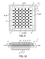
- the OLED 35 comprises a particular terminal structure. It shows the anode connector 33 and four (4) cathode connectors 32 _left, 32 _right, 32 _top and 32 _bottom on either side (see also top view of FIG. 9 ).
- the anode connector 33 extends seamlessly into the anode layer 33 a with which it forms a rectangular structure.
- the cathode connectors 32 _left, 32 _right, 32 _top and 32 _bottom basically also extend seamlessly into the cathode layer 32 a , but each cathode connector 32 _left, 32 _right, 32 _top and 32 _bottom shows a rectangular shape in itself which extends outwardly from the cathode layer 32 a .
- a layer 36 having inductive properties which in the present case is a ferromagnetic layer 36 , covers the cathode layer 32 a .
- a common anode layer 33 a is provided.
- cathode connectors 32 ( 32 _left, 32 _right, 32 _top, 32 _bottom) are designed, each of which is located on one of the sides of the OLED 35 so that, in analogy with FIG. 4 a , individual generators 3 a _left, 3 b _right, 3 a _top and 3 b _bottom can be connected.
- either more than four (>4) or fewer than four ( ⁇ 4) cathode connectors 32 _left, 32 _right, 32 _top and 32 _bottom are possible.
- the location of said cathode connectors 32 _left, 32 _right, 32 _top and 32 _bottom may vary according to demand without departing from the scope of the invention.
- FIG. 9 shows schematically the OLED 35 of which part of the cover 31 is removed. Hence, the view is directed into the open OLED 35 . The direction of light emission is situated in the plane of the drawing. In the four corners, parts of the hermetic cover 31 are still visible. The ferromagnetic layer 36 is visible on top of the open OLED 35 .
- discrete inductors L are symbolically visualized in a rectangular structure on the surface of the ferromagnetic layer 36 in order to link the function of the ferromagnetic layer 36 with the inductors L in the explanation of the principle of operation of the invention, based on the one-dimensional and two-dimensional discrete elements.
- the ferromagnetic layer 36 is adjacent to the cathode layer 32 a .
- the ferromagnetic layers 36 may be chosen from a material having certain optical properties, i.e. properties of reflecting the light, reflecting light only in a specific wavelength range, being transmissive to light, etc.
- the ferromagnetic layer 36 or more generally the structure for realizing an inductive property—may be e.g. glued on the stacked structure of the OLED 35 or pressed onto the OLED 35 by means of the cover 31 .
- the cover 31 may also be made of a ferromagnetic material.
- omission of an additional ferromagnetic layer 36 but use of the electrode connectors 32 , 32 a and 33 , 33 a instead may also realize the inductive behavior, provided that the inductivity achieved by the electrode connectors 32 , 32 a and 33 , 33 a can be realized to show a sufficient value.
- the electrodes 32 a and 33 a alone or in combination with the electrode connectors 32 and 33 or in combination with the ferromagnetic layer 36 may realize the delay structure.
- the inductive behavior may be tuned according to demand by adding coils or using coils in combination with the ferromagnetic layer 36 .
- a transparent ferromagnetic layer applied to the anode layer 33 a may also realize the inductive function of the ferromagnetic layer 36 in the context of utilizing the anode layer 33 a for realizing the inductive function of the OLED 35 .
- FIG. 10 shows a further embodiment comprising a structured or segmented anode layer 33 a
- the cathode layer 32 a is designed as a plane-shaped unit with a common connector 32 .
- printed coils L may be used to realize the structured or segmented anode layer 33 a .
- FIG. 11 is a schematic top view of an example of a part of such a structured anode layer 33 a . It allows creating pixel segmentation but also free forms such as e.g. a heart or an arrow as visualized in FIG. 10 . Other pre-defined symbols are also possible.
- inductive function on the cathode layer 32 a as well as on the anode layer 33 a in one design. Therefore, printed coils with some ferromagnetic layer can be established on/in both layers 32 a and 33 a .
- a relatively high inductance value per unit of area (or length) can be achieved, such that power signal propagation is slowed down in comparison with lower inductive values.
- the various embodiments of realizing the delay structure within the OLED 35 provide an inventive method of operating an OLED 35 . It comprises the steps of receiving, with reference to a reference potential, at least two power signal pulses 4 a _left, 4 b _right, 4 a _top, 4 b _bottom, wherein the at least two power signal pulses 4 a _left, 4 b _right, 4 a _top, 4 b _bottom have a temporal relationship with one another and such a signal strength that a part of the light-emitting structure is powered or driven accordingly when the power signal pulses 4 a _left, 4 b _right, 4 a _top, 4 b _bottom coincide at said part of the light-emitting structure; feeding the at least two power signal pulses 4 a _left, 4 b _right, 4 a _top, 4 b _bottom into a delay structure of the OLED at different positions of the delay structure; delaying a propagation of the at
- the receiving step is herein performed by means of a plurality of cathode connectors 32 or anode connectors 33 , as the case may be, wherein each connector 32 or 33 is assigned to the individual power signal pulses 4 a _left, 4 b _right, 4 a _top, and 4 b _bottom.
- the delaying step is performed with the aid of a capacitive element realized by means of the light-emitting structure (uniform or segmented) of the OLED 35 .
- the delaying step is performed with the aid of an inductive element realized by way of a discrete or a continuum-like embodiment, as explained in detail above.
- FIGS. 6 a to 6 d A simulation of the OLED according to the invention will finally lead to the similar results as already visualized in FIGS. 6 a to 6 d , wherein different resultant light intensity distributions depending on different power signal pulse amplitudes and delay settings are visualized.
- OLEDs show some current distribution errors leading to a degraded brightness in the center of the OLED. Therefore, an appropriate parameter setting can be chosen in order to compensate for this degradation.
- the concept of this compensation is given by the result shown in FIG. 6 a .
- a direct current DC signal with power signal pulse trains for the remaining 10% of the time can compensate for these current distribution errors.
- the second generator 3 b is substituted by e.g. a wire 15 which short-circuits the extreme right end of the propagation line, which leads to an unmatched termination.
- the first generator 3 a shows a particular design taking this circumstance into account, as shown in FIG. 12 b .
- the Figure shows a signal source 3 c , a MOS-FET full bridge inverter structure 3 d , which comprises four (4) NMOS transistors M 1 to M 4 , and a source resistor 3 e which, for providing matched conditions, is designed to have an impedance Z which has the same value as the impedance Z of the propagation line.
- This design allows generating power signal pulses 4 a and 4 b having a positive polarity as well as a negative polarity.
- Other design implementations may also provide a solution for generating bipolar power signal pulses.
- the first power signal pulse 4 a having a negative polarity is generated with a signal strength of ⁇ 0.75 VF.
- the first power signal pulse 4 a thus generated propagates along the propagation line and the OLEDs are not powered because of the negative polarity.
- the first power signal pulse 4 a reaches the end of the propagation line, where it is reflected.
- the reflected first power signal pulse 4 a is now labeled as the second power signal pulse 4 b and propagates along the propagation line with a positive polarity and a signal strength of 0.75 ⁇ VF in the direction back to the first pulse generator 3 a .
- This is similar to the first embodiment, in which a second pulse generator 3 b is provided for generating the second power signal pulse 4 b . Given this signal strength of the second power signal pulse 4 b , still none of the OLEDs is powered. Without any superposition with another power signal pulse, the second power signal pulse 4 b would simply travel along the propagation line and be dissipated by the source resistance 3 e .
- this further first power signal pulse 4 a does not power any of the OLEDs when travelling along the propagation line.
- the two power signal pulses 4 a and 4 b overlap constructively and result in the pulse 8 showing a signal strength of 1.5 VF if no OLEDs are present as described hereinbefore.
- the voltage V is truncated (not shown in FIG. 5 a ) at a certain level, and at least part of the signal energy is supplied to the OLED or OLEDs located at this position.
- a general timing condition allowing the pulses to overlap constructively is given by the following equation: 0 ⁇ dt ⁇ n ⁇ t seg (Equation 6)
- the two power signal pulses 4 a and 4 b will miss each other.
- the theoretical model described herein needs to be adapted if the pulse duration is longer than n ⁇ t seg because it is assumed in the present model that the pulse duration is shorter than n ⁇ t seg .
- addressing the last OLED could be difficult.
- applying a dummy segment or delay element, e.g. without any OLED could solve this problem.
- FIG. 13 a is a scheme of operation by means of traveling power signal pulses 4 a and 4 b that overlap and result in the pulse 8 at a particular element (in the present case at the box E 6 ) after the (negative) first power signal pulse 4 a was reflected at the end of the propagation line.
- This scheme of operation reflects the timing as described above.
- the time line t extending from top to bottom is shown on the left side of the timing diagrams.
- the first power signal pulse 4 a is released.
- the (positive) further first signal pulse 4 a is released.
- the two pulses 4 a and 4 b overlap.
- the superposition takes place at the location of the box E 6 .
- the first generator 3 a and the boxes E 1 to E 15 and the wire 15 realizing the end of the propagation line are shown at the top of FIG. 13 a only in a very schematic manner and in reality are connected to each other as shown in detail in FIG. 12 a.
- FIG. 13 b shows simulation results for a circuit 1 as shown in FIGS. 12 a and 12 b .
- the parameters applied in this model are identical to the parameters applied in the model described with reference to the first embodiment.
- the delay times t delay are shown in the following Table:
- Reference numeral 16 17 18 Delay time 10 ⁇ s 30 ⁇ s 55 ⁇ s
- the peak current for OLED current 17 should occur exactly at OLED position number eighteen (18). However, a slight deviation from the desired result is visible in the model result. Because of circumstances related to the modeling of the circuit 1 , a correction of minus two ( ⁇ 2) ⁇ s of the delay time dt seems to be applicable in the present case.
- the power signal pulse energy is dissipated and some of it still propagates along the propagation line. This further propagating energy may cause undesired powering or addressing of OLEDs if another power signal pulse is released at a too early instant. Given this non-ideal dissipation, it may happen that e.g. the further first power signal pulse 4 a (or more precisely the non-dissipated part of it) continues propagating towards the end of the propagation line where it is reflected with a negative polarity and propagates towards the generator 3 a . If a further negative pulse is now generated at a too early instant—e.g.
- This design does not require any additional wires or cables for connecting the first end of the propagation line with the second end of the propagation line for the purpose of transmitting control signals or providing a mains connection or power supply connection for a second generator.
- this single generator powered design is perfectly suited for realizing long light sources, such as OLED tubes/bars showing e.g. a traveling light spot or light bar.
- the generator 3 a or the generators 3 a and 3 b may be designed to generate a negative bias voltage within the boundaries of the breakthrough voltage of the OLEDs applied in the circuit 1 .
- This solution enables higher amplitudes of the power signal pulses to be generated and released into the propagation line in order to achieve a higher brightness for the selected OLED without accidentally powering additional (neighboring) OLEDs as described in the embodiments above.
- a positive bias voltage may be a design choice.
- the positive bias voltage may be selected to be just below the forward voltage of the OLEDs. This design enables the use of relatively low power signal pulse amplitudes to be generated by the generator(s) 3 a (and 3 b ). It would improve the efficiency because only a power signal pulse 4 a (and 4 b ) with a small amplitude would need to be released into the propagation line via the impedance-matching impedance. However, this design choice requires relatively low impedance inductivities L in order to allow proper operation.
- power signal pulses are not only fed into the delay structure at the outermost edges of the OLED but may also be fed at particular positions within the structure of the OLED.
- This can be achieved by connecting a part of the electrode connectors e.g. by means of tiny (transparent) wires or conductors with an inner part of the delay structure.
- An additional interconnecting layer can also be provided for this purpose.
- a part (or area) of the electrode layer may be used to connect an inner part of the delay structure with the connector. The principle of operation of such an embodiment is explained with reference to FIG. 14 in the context of a one-dimensional delay structure. It explains the feeding of the power signal pulses not only from the outermost boundaries of e.g.
- FIG. 14 comprises a third generator 19 in addition to the components already described with reference to FIG. 1 .
- the generator 19 is designed to produce a third power signal pulse 4 c .
- It is connected with an additional matching impedance 20 which is designed to have half the value of the characteristic impedance Z of the propagation line.
- a delay element-like structure which comprises an inductor 21 , a capacitor 22 and a switch 23 .
- the switch 23 is connected with the propagation line at the location of one of the OLEDs.
- the value of the inductor 21 is designed to have half the value of the inductors L of the propagation line, and the value of the capacitor 22 is designed to be twice as high as the value of the capacitors C of the propagation line.
- the switch 23 is provided to either connect the elements 19 to 22 with, or to disconnect them completely from the propagation line.
- the design allows introducing additional power signal pulses 4 c between the tenth (10 th ) box E 10 and the eleventh (11 th ) box E 11 of the delay line so that the introduced additional power signal pulses 4 c can propagate in both directions along the propagation line.
- a real-world application which may comprise e.g.
- E 30 blocks E 1 to E 30 , there may be a further group of elements 19 to 23 which is connected between the nineteenth (19 th ) box E 19 and the twentieth (20 th ) box E 20 .
- This allows defining three sections of the delay line, e.g. E 1 to E 10 , E 11 to E 19 and E 20 to E 30 .
- the two additional power generators 19 can be used to support this as it fits best. If e.g. OLED number five (5) needs to be powered, it will be advantageous to use the first generator 3 a in combination with the additional third generator 19 connected at OLED number ten (10).
- the second power signal pulse 4 b released from the second generator 3 b would need to travel a relatively long distance before reaching the OLED number five (5) and would thus run the risk of degradation because of non-ideal component characteristics of the propagation line.
- two additional generators 19 are mentioned in the embodiments described above, it is to be noted that any other number can be applied as well.
- various feeding points for feeding the additional power signal pulses 4 c generated by the additional generator or generators 19 can be selected according to demand.
- a third generator with matching circuitry may be connected to several switches 23 which couple the power signal pulse into several feeding ports.
- generator 3 a or 3 b may be used together with additional switches and, if necessary, additional matching circuitry instead of the third power signal generator 19 .
- the principle of feeding power signal pulses to a particular position inside the delay line, as described above, can also be used with multi-dimensional structures, e.g. the delay plane inside the OLED. Again, suitable values for the matching impedances 2 have to be selected.
- the OLED according to the invention is typically used in the field of general illumination or more particularly in the field of local highlighting in signal lighting applications or backlighting for vehicles, general topics of creating decorative effects, as well as in the domain of guiding lights.
- the OLED according to the invention is typically used in the field of general illumination or more particularly in the field of local highlighting in signal lighting applications or backlighting for vehicles, general topics of creating decorative effects, as well as in the domain of guiding lights.
- the OLED according to the invention is typically used in the field of general illumination or more particularly in the field of local highlighting in signal lighting applications or backlighting for vehicles, general topics of creating decorative effects, as well as in the domain of guiding lights.
- the OLED according to the invention can be realized either by means of timing the power signal pulses or by segmentation, even display-like applications can be realized with the OLED according to the invention.
- the control unit 6 may cooperate with a central processing unit of the respective device for receiving control signals or commands to be interpreted by the control unit 6 .
- the control unit 6 may control the position of the light-emitting area within the light-emitting structure of an OLED to be illuminated in accordance with the description above, but it may additionally control the frequency as well as the intensity of the illumination. Varying the rate of selecting individual areas of the OLED but also varying the form or shape or duration of the individual power signal pulses 4 a and 4 b may serve this purpose as well. In some embodiments, even completely transparent OLED structures may be used, which give the impression that a glass window emits light when the OLED is switched on.
Abstract
Description
t seg =√{square root over (L·C)} (Equation 2)
dt=t right −t left (Equation 3)
|dt|≦n·t seg (Equation 4)
t delay=(2·n sel−(n+1))·t seg (Equation 5)
| |
||
| 9 | 10 | 11 | 12 | 13 | 14 | ||
| Delay time | −25 μs | −5 |
0 |
10 |
20 |
25 μs |
0≦dt≦n·t seg (Equation 6)
t delay=(n−n sel)·2·t seg (Equation 7)
| |
|||
| 16 | 17 | 18 | |||
| |
10 |
30 μs | 55 μs | ||
t=t2+2n·t seg (Equation 8)
Claims (18)
Applications Claiming Priority (4)
| Application Number | Priority Date | Filing Date | Title |
|---|---|---|---|
| EP08170795 | 2008-12-05 | ||
| EP08170795 | 2008-12-05 | ||
| EP08170795.2 | 2008-12-05 | ||
| PCT/IB2009/055398 WO2010064184A1 (en) | 2008-12-05 | 2009-11-30 | Oled with integrated delay structure |
Publications (2)
| Publication Number | Publication Date |
|---|---|
| US20110234097A1 US20110234097A1 (en) | 2011-09-29 |
| US8686660B2 true US8686660B2 (en) | 2014-04-01 |
Family
ID=41682259
Family Applications (1)
| Application Number | Title | Priority Date | Filing Date |
|---|---|---|---|
| US13/132,334 Active 2030-08-27 US8686660B2 (en) | 2008-12-05 | 2009-11-30 | OLED with integrated delay structure |
Country Status (8)
| Country | Link |
|---|---|
| US (1) | US8686660B2 (en) |
| EP (1) | EP2374121B1 (en) |
| JP (1) | JP5777252B2 (en) |
| KR (2) | KR20110098937A (en) |
| CN (1) | CN102239512B (en) |
| RU (1) | RU2514205C2 (en) |
| TW (1) | TW201031247A (en) |
| WO (1) | WO2010064184A1 (en) |
Families Citing this family (7)
| Publication number | Priority date | Publication date | Assignee | Title |
|---|---|---|---|---|
| US8188463B2 (en) * | 2009-11-19 | 2012-05-29 | General Electric Company | Organic light emitting diode with magnetic structure for improved current adaptability |
| IN2014CN02649A (en) | 2011-10-21 | 2015-08-07 | Koninkl Philips Nv | |
| JP6339019B2 (en) * | 2011-12-12 | 2018-06-06 | フィリップス ライティング ホールディング ビー ヴィ | Circuit arrangement for selectively powering distributed loads |
| CN104094437A (en) * | 2012-02-02 | 2014-10-08 | 皇家飞利浦有限公司 | Light apparatus for generating light |
| CN104269431B (en) * | 2014-09-29 | 2017-03-01 | 京东方科技集团股份有限公司 | A kind of organic elctroluminescent device, its driving method and display device |
| CN110969982B (en) * | 2018-09-28 | 2022-09-13 | 北京小米移动软件有限公司 | Display structure, display panel and display device |
| DE102019122474B9 (en) | 2019-08-21 | 2023-03-02 | OSRAM Opto Semiconductors Gesellschaft mit beschränkter Haftung | DRIVE METHOD AND DISPLAY DEVICE |
Citations (5)
| Publication number | Priority date | Publication date | Assignee | Title |
|---|---|---|---|---|
| EP0154662A1 (en) | 1984-03-15 | 1985-09-18 | Hans Werba | Optical line display |
| US5519414A (en) * | 1993-02-19 | 1996-05-21 | Off World Laboratories, Inc. | Video display and driver apparatus and method |
| WO1996015519A1 (en) | 1994-11-09 | 1996-05-23 | Off World Laboratories, Inc. | Video display and driver apparatus and method |
| EP1169695A1 (en) | 1999-04-02 | 2002-01-09 | Sun Microsystems, Inc. | Method and apparatus for selective enabling of addressable display elements, specially for arrangements with image signal propagation along a display conductor with tap points |
| US7019721B2 (en) * | 2003-04-24 | 2006-03-28 | Naamloze Vennootschap, Barco | Organic light-emitting diode drive circuit for a display application |
Family Cites Families (4)
| Publication number | Priority date | Publication date | Assignee | Title |
|---|---|---|---|---|
| US5707745A (en) * | 1994-12-13 | 1998-01-13 | The Trustees Of Princeton University | Multicolor organic light emitting devices |
| JP2003140610A (en) * | 2001-10-31 | 2003-05-16 | Canon Electronics Inc | Organic electroluminescence panel and method for driving the same |
| JP2004191752A (en) * | 2002-12-12 | 2004-07-08 | Seiko Epson Corp | Electrooptical device, driving method for electrooptical device, and electronic equipment |
| RU2326448C2 (en) * | 2005-09-23 | 2008-06-10 | Самсунг Электроникс Ко., Лтд. | Liquid crystal display |
-
2009
- 2009-11-30 JP JP2011539142A patent/JP5777252B2/en active Active
- 2009-11-30 EP EP09775306.5A patent/EP2374121B1/en active Active
- 2009-11-30 CN CN200980149167.1A patent/CN102239512B/en active Active
- 2009-11-30 KR KR1020117015409A patent/KR20110098937A/en not_active Application Discontinuation
- 2009-11-30 US US13/132,334 patent/US8686660B2/en active Active
- 2009-11-30 RU RU2011127403/07A patent/RU2514205C2/en active
- 2009-11-30 KR KR1020187001117A patent/KR101944382B1/en active IP Right Grant
- 2009-11-30 WO PCT/IB2009/055398 patent/WO2010064184A1/en active Application Filing
- 2009-12-03 TW TW098141458A patent/TW201031247A/en unknown
Patent Citations (5)
| Publication number | Priority date | Publication date | Assignee | Title |
|---|---|---|---|---|
| EP0154662A1 (en) | 1984-03-15 | 1985-09-18 | Hans Werba | Optical line display |
| US5519414A (en) * | 1993-02-19 | 1996-05-21 | Off World Laboratories, Inc. | Video display and driver apparatus and method |
| WO1996015519A1 (en) | 1994-11-09 | 1996-05-23 | Off World Laboratories, Inc. | Video display and driver apparatus and method |
| EP1169695A1 (en) | 1999-04-02 | 2002-01-09 | Sun Microsystems, Inc. | Method and apparatus for selective enabling of addressable display elements, specially for arrangements with image signal propagation along a display conductor with tap points |
| US7019721B2 (en) * | 2003-04-24 | 2006-03-28 | Naamloze Vennootschap, Barco | Organic light-emitting diode drive circuit for a display application |
Also Published As
| Publication number | Publication date |
|---|---|
| JP2012511172A (en) | 2012-05-17 |
| TW201031247A (en) | 2010-08-16 |
| JP5777252B2 (en) | 2015-09-09 |
| US20110234097A1 (en) | 2011-09-29 |
| KR20110098937A (en) | 2011-09-02 |
| KR101944382B1 (en) | 2019-02-07 |
| CN102239512A (en) | 2011-11-09 |
| EP2374121B1 (en) | 2019-09-04 |
| KR20180010314A (en) | 2018-01-30 |
| CN102239512B (en) | 2014-12-17 |
| WO2010064184A1 (en) | 2010-06-10 |
| EP2374121A1 (en) | 2011-10-12 |
| RU2011127403A (en) | 2013-01-10 |
| RU2514205C2 (en) | 2014-04-27 |
Similar Documents
| Publication | Publication Date | Title |
|---|---|---|
| US8686660B2 (en) | OLED with integrated delay structure | |
| CN103000132B (en) | Pixel driving circuit and display panel | |
| CN104036698B (en) | It is integrated with the display device and its driving method of touch screen panel | |
| TWI432087B (en) | An arrangement for driving led cells | |
| CN106469539A (en) | Display panel and pixel circuit | |
| US10984704B2 (en) | Display device | |
| TW201434024A (en) | Organic light emitting display | |
| CN202150459U (en) | AMOLED display | |
| CN103366677A (en) | Display apparatus | |
| KR101706578B1 (en) | backlight unit and liquid crystal display module including the same | |
| CN106325603A (en) | Touch display panel and device | |
| KR20050048711A (en) | Electro luminescence display contained emi shielding means | |
| CN110060633A (en) | A kind of display panel, its driving method and display device | |
| KR102646656B1 (en) | Transparent light-emitting diode film | |
| CN110162224A (en) | Touch display substrate and its driving method, display device | |
| KR102584274B1 (en) | Pixel and display apparatus | |
| CN111583852B (en) | Light-emitting panel, control method of light-emitting panel, and display device | |
| CN203070738U (en) | Pixel driving circuit and display panel | |
| WO2010064183A1 (en) | Circuit for and method of selectively powering a plurality of load elements | |
| US9615411B2 (en) | Backlight unit including a power transmitting wire | |
| US9148913B2 (en) | Backlight module transmitting electricity through magnetic field induction | |
| JP2004240156A (en) | Driving device for light emitting display panel | |
| JP2011170290A (en) | Display device | |
| TW201214388A (en) | Switchable organic electro-luminescence display panel and switchable organic electro-luminescence display circuit | |
| Casas et al. | Electronic System for Graphical Representation on Cooking Surfaces of Domestic Induction Hobs |
Legal Events
| Date | Code | Title | Description |
|---|---|---|---|
| AS | Assignment |
Owner name: KONINKLIJKE PHILIPS ELECTRONICS N V, NETHERLANDS Free format text: ASSIGNMENT OF ASSIGNORS INTEREST;ASSIGNOR:RADERMACHER, HARALD JOSEF GUNTHER;REEL/FRAME:026375/0020 Effective date: 20100929 |
|
| STCF | Information on status: patent grant |
Free format text: PATENTED CASE |
|
| MAFP | Maintenance fee payment |
Free format text: PAYMENT OF MAINTENANCE FEE, 4TH YEAR, LARGE ENTITY (ORIGINAL EVENT CODE: M1551) Year of fee payment: 4 |
|
| AS | Assignment |
Owner name: KONINKLIJKE PHILIPS N.V., NETHERLANDS Free format text: CHANGE OF NAME;ASSIGNOR:KONINKLIJKE PHILIPS ELECTRONICS N.V.;REEL/FRAME:047407/0258 Effective date: 20130515 Owner name: KONINKLIJKE PHILIPS ELECTRONICS N.V., NETHERLANDS Free format text: CHANGE OF ADDRESS;ASSIGNOR:KONINKLIJKE PHILIPS ELECTRONICS N.V.;REEL/FRAME:046703/0202 Effective date: 20091201 |
|
| AS | Assignment |
Owner name: BEIJING XIAOMI MOBILE SOFTWARE CO., LTD., CHINA Free format text: ASSIGNMENT OF ASSIGNORS INTEREST;ASSIGNOR:KONINKLIJKE PHILIPS N.V.;REEL/FRAME:046633/0913 Effective date: 20180309 |
|
| MAFP | Maintenance fee payment |
Free format text: PAYMENT OF MAINTENANCE FEE, 8TH YEAR, LARGE ENTITY (ORIGINAL EVENT CODE: M1552); ENTITY STATUS OF PATENT OWNER: LARGE ENTITY Year of fee payment: 8 |