US8723654B2 - Interrupt generation and acknowledgment for RFID - Google Patents
Interrupt generation and acknowledgment for RFID Download PDFInfo
- Publication number
- US8723654B2 US8723654B2 US12/833,861 US83386110A US8723654B2 US 8723654 B2 US8723654 B2 US 8723654B2 US 83386110 A US83386110 A US 83386110A US 8723654 B2 US8723654 B2 US 8723654B2
- Authority
- US
- United States
- Prior art keywords
- memory
- rfid
- interface
- interrupt
- circuit
- Prior art date
- Legal status (The legal status is an assumption and is not a legal conclusion. Google has not performed a legal analysis and makes no representation as to the accuracy of the status listed.)
- Active, expires
Links
Images


Classifications
-
- G—PHYSICS
- G06—COMPUTING; CALCULATING OR COUNTING
- G06K—GRAPHICAL DATA READING; PRESENTATION OF DATA; RECORD CARRIERS; HANDLING RECORD CARRIERS
- G06K19/00—Record carriers for use with machines and with at least a part designed to carry digital markings
- G06K19/06—Record carriers for use with machines and with at least a part designed to carry digital markings characterised by the kind of the digital marking, e.g. shape, nature, code
- G06K19/067—Record carriers with conductive marks, printed circuits or semiconductor circuit elements, e.g. credit or identity cards also with resonating or responding marks without active components
- G06K19/07—Record carriers with conductive marks, printed circuits or semiconductor circuit elements, e.g. credit or identity cards also with resonating or responding marks without active components with integrated circuit chips
- G06K19/0701—Record carriers with conductive marks, printed circuits or semiconductor circuit elements, e.g. credit or identity cards also with resonating or responding marks without active components with integrated circuit chips at least one of the integrated circuit chips comprising an arrangement for power management
- G06K19/0707—Record carriers with conductive marks, printed circuits or semiconductor circuit elements, e.g. credit or identity cards also with resonating or responding marks without active components with integrated circuit chips at least one of the integrated circuit chips comprising an arrangement for power management the arrangement being capable of collecting energy from external energy sources, e.g. thermocouples, vibration, electromagnetic radiation
- G06K19/0708—Record carriers with conductive marks, printed circuits or semiconductor circuit elements, e.g. credit or identity cards also with resonating or responding marks without active components with integrated circuit chips at least one of the integrated circuit chips comprising an arrangement for power management the arrangement being capable of collecting energy from external energy sources, e.g. thermocouples, vibration, electromagnetic radiation the source being electromagnetic or magnetic
- G06K19/0709—Record carriers with conductive marks, printed circuits or semiconductor circuit elements, e.g. credit or identity cards also with resonating or responding marks without active components with integrated circuit chips at least one of the integrated circuit chips comprising an arrangement for power management the arrangement being capable of collecting energy from external energy sources, e.g. thermocouples, vibration, electromagnetic radiation the source being electromagnetic or magnetic the source being an interrogation field
Definitions
- the invention relates, in general, to the field of radio frequency identification (RFID) systems. More particularly, the invention relates in part to an RFID transponder incorporating FRAM memory. The invention also relates to a modified serial interface that has utility within and beyond RFID applications.
- RFID radio frequency identification
- a basic RFID system includes three components: an antenna or coil; a transceiver with decoder, i.e., RFID reader; and a transponder, i.e., RFID tag, programmed with unique information.
- RFID tags are categorized as either active or passive. Active RFID tags are powered by an internal battery and are typically read/write, i.e., tag data can be rewritten and/or modified. Passive RFID tags operate without a separate external power source and obtain operating power generated from the reader.
- Tag 100 includes an antenna 102 that is coupled to an analog front end circuit 104 , which is in communication with a digital and memory circuit 106 through receive (RX) and transmit (TX) paths.
- RX receive
- TX transmit
- EEPROM electrically erasable programmable read-only memory
- the EPC Global Generation 2 standard includes a published method of doing Block Writes to memory. This method is inefficient when considering the capability of faster memory technologies, such as FRAM memory.
- the present invention is directed to an interrupt controller circuit for an RFID application that substantially obviates one or more of the problems due to limitations and disadvantages of the related art.
- a memory circuit includes a memory, a memory access control circuit coupled to the memory, an RFID interface coupled to the memory access control circuit, a secondary interface coupled to the memory access control circuit, and an interrupt manager coupled to the memory access control circuit, the RFID interface, and the secondary interface.
- FIG. 1 is a block diagram of a prior art EEPROM based passive RFID tag
- FIG. 2 is a block diagram of a FRAM memory based passive RFID tag according to the present invention.
- FIG. 3 is a block diagram of an embedded FRAM memory based RFID application
- FIG. 4 is a further detailed block diagram of the digital portion of the FRAM based RFID circuit shown in FIGS. 2 and 3 ;
- FIG. 5 is a further detailed block diagram of the serial interface of the FRAM based RFID circuit shown in FIGS. 2 and 3 ;
- FIGS. 6-10 are timing diagrams associated with the serial interface circuit shown in FIG. 5 ;
- FIG. 11 is a block diagram of a memory pointer circuit associated with the digital portion of the FRAM based RFID circuit shown in FIGS. 2 and 3 ;
- FIG. 12 is a portion of the memory contents associated with the memory pointer circuit of FIG. 11 ;
- FIG. 13 is a flow chart of a prior art technique for reading and writing data to memory
- FIG. 14 is a flow chart of another prior art technique for reading and writing data to memory
- FIG. 15 is a flow chart of a technique according to the present invention for reading and writing data to memory using the memory point circuit of FIG. 11 ;
- FIG. 16 is an EPC global BlockWrite command data structure according to the prior art
- FIGS. 17A and 17B taken together represent a flow chart of a prior art method for implementing the BlockWrite command
- FIGS. 18A and 18B taken together represent a flow chart of a method for implementing the BlockWrite command according to the present invention
- FIG. 19 is an alternative block diagram representation of a portion of the digital circuitry associated with the circuits of FIGS. 2 and 3 , according to the present invention, including an interrupt manager block;
- FIGS. 20A and 20B taken together represent a flow chart for performing an interrupt method according to the invention, associated with the interrupt manager block of FIG. 19 .
- a passive RFID tag 200 includes an antenna 202 , an analog front end 204 , and a digital portion 206 that includes digital control circuitry and FRAM memory and communicates with the analog front end 204 using the RX and TX paths. Additionally, RFID tag 200 includes a serial interface bus 208 coupled to pins 210 . A four bit wide bus 208 is shown in FIG. 2 . The analog and digital portions of the RFID circuit 204 and 206 are normally integrated on to one or more integrated circuits. In the common/usual passive tag implementation shown in FIG. 2 , the serial interface is normally not present and pins 210 are not used.
- an embedded RFID application 300 includes an RFID integrated circuit 314 , which contains the analog front end 304 and the digital and FRAM memory portion 306 .
- the antenna 302 may or may not be actually included in the RFID integrated circuit 314 .
- four pins 310 associated with the serial interface of the digital portion 316 are brought out.
- the four pins 310 are the chip select, clock, DATA 1 , and DATA 2 pins, which are explained in further detail below.
- the serial interface is typically coupled to a microprocessor 312 , which is in communication with various control inputs associated with the RFID application 300 .
- a typical application 300 could be a metering application, or a control application for a factory.
- the RFID integrated circuit 314 in a typical embedded application would be interrogated from time to time with a handheld reader (not shown in FIG. 3 ).
- Digital portion 406 includes the RX and TX paths for reference with FIGS. 2 and 3 .
- the RX and TX paths are in communication with a state machine 420 that is in bi-directional communication with FRAM memory block 422 .
- An arbitration logic block 424 is associated with FRAM memory 422 , and is used to bi-directionally control serial interface 426 .
- serial interface 426 is coupled through a four bit bus to external pins 410 .
- serial interface 426 of FIG. 4 As known in the art, a conventional SPI interface has four pins: Select, Clock, DataIn, and DataOut. To transfer one byte of data, either in or out, requires eight clock cycles, in addition to the data dependent transitions on the single data line.
- the serial interface 500 shown in FIG. 5 appears to be similar to a SPI interface, but there are two important improvements. First, both data ports are used as a bidirectional pair. Second, both edges of the clock are used to shift or transfer data. With both of these improvements, only a pair of clock cycles is used to transfer a byte of data. The power used in data transitions is constant, but the power used for clock transitions is cut by a factor of four.
- serial interface 500 shown in FIG. 5 is but one of the features for improving throughput in a FRAM memory based passive RFID tag or circuit, although it has utility in non-RFID applications as well. Specifically, serial interface 500 minimizes the number of clock transitions required to transmit a data word when compared to the convention SPI interface, while retaining the same pin count.
- serial interface 500 includes a Select pin, a Clock pin, a bidirectional Data_ 1 pin, and a bidirectional Data_ 0 pin.
- the Select pin is coupled to an OpCode Interpreter and State Machine 504 , which is realized in conventional logic circuits.
- State machine 504 is in bidirectional communication with Data Out register 502 and Data In register 506 .
- Data Out register 502 is coupled through a 16 bit bus, which branches to two 8 bit busses, to shift register 508 A and shift register 508 C.
- Data In register is coupled through a 16 bit bus, which branches to two 8 bit busses, to shift register 508 B and 508 D.
- Shift register 508 A loads data onto the Data_ 1 pin
- shift register 508 B receives data from the Data_ 1 pin
- shift register 508 C loads data onto the Data_ 0 pin
- shift register 508 D receives data from the Data_ 0 pin.
- Shift registers 508 A through 508 D are operated by alternative clock cycles through inverters 510 and 512 .
- the clocking and transfer scheme of the serial interface 500 is further explained with respect to the timing diagrams of FIGS. 6-10 .
- the state machine Based on the received command, the state machine produces the read or write control signal. It also transfers the address and data from the shift registers and applies them to the FRAM as appropriate.
- the write cycle for 16 bits of information is shown.
- the CS Chip Select signal goes high, and, after a predetermined delay time of t CSU , the write cycle begins.
- the D 1 data word includes a R/W bit, opcode information, and five address bits.
- An opcode can include information regarding an operational mode such as “test”, “normal”, “status”, or “control”.
- the D 1 data word includes eight data bits which will be written to the FRAM memory.
- the D 0 data word includes opcode information and five address bits.
- the D 0 data word includes eight data bits, also written to the FRAM memory.
- the read cycle for 16 bits of information is shown.
- the CS Chip Select signal goes high, and, after a predetermined delay time of t CSU , the read cycle begins.
- the D 1 data word also includes a R/W bit, opcode information, and five address bits.
- the D 1 data word includes eight data bits from the FRAM memory.
- the D 0 data word also includes opcode information and five address bits.
- the D 0 data word includes eight data bits, also from the FRAM memory.
- the first high transition of the CLK signal is used to transfer the R/W bit on D 1 and to transfer the OP 4 bit on D 0 .
- the first low transition of the CLK signal is used transfer the OP 3 bit on D 1 and to transfer the OP 2 bit on D 0 .
- the second high transition of the CLK signal is used to transfer the OP 1 bit on D 1 and to transfer the OP 0 bit on D 0 .
- the second low transition of the CLK signal is used transfer the A 9 bit on D 1 and to transfer the A 8 bit on D 0 .
- the third high transition of the CLK signal is used to transfer the A 7 bit on D 1 and to transfer the A 6 bit on D 0 .
- the third low transition of the CLK signal is used transfer the A 5 bit on D 1 and to transfer the A 4 bit on D 0 .
- the fourth high transition of the CLK signal is used to transfer the A 3 bit on D 1 and to transfer the A 2 bit on D 0 .
- the fourth low transition of the CLK signal is used transfer the A 1 bit on D 1 and to transfer the A 0 bit on D 0 .
- the first high transition of the CLK signal is used to transfer the D 15 bit on D 1 and to transfer the D 14 bit on D 0 .
- the first low transition of the CLK signal is used transfer the D 13 bit on D 1 and to transfer the D 12 bit on D 0 .
- the second high transition of the CLK signal is used to transfer the D 11 bit on D 1 and to transfer the D 10 bit on D 0 .
- the second low transition of the CLK signal is used transfer the D 9 bit on D 1 and to transfer the D 8 bit on D 0 .
- the third high transition of the CLK signal is used to transfer the D 7 bit on D 1 and to transfer the D 6 bit on D 0 .
- the third low transition of the CLK signal is used transfer the D 5 bit on D 1 and to transfer the D 4 bit on D 0 .
- the fourth high transition of the CLK signal is used to transfer the D 3 bit on D 1 and to transfer the D 2 bit on D 0 .
- the fourth low transition of the CLK signal is used transfer the D 1 bit on D 1 and to transfer the D 0 bit on D 0 .
- the first high transition of the CLK signal is used to drive the D 15 bit on D 1 and to transfer the D 14 bit on D 0 .
- the first low transition of the CLK signal is used transfer the D 13 bit on D 1 and to transfer the D 12 bit on D 0 .
- the second high transition of the CLK signal is used to transfer the D 11 bit on D 1 and to transfer the D 10 bit on D 0 .
- the second low transition of the CLK signal is used transfer the D 9 bit on D 1 and to transfer the D 8 bit on D 0 .
- the third high transition of the CLK signal is used to transfer the D 7 bit on D 1 and to transfer the D 6 bit on D 0 .
- the third low transition of the CLK signal is used transfer the D 5 bit on D 1 and to transfer the D 4 bit on D 0 .
- the fourth high transition of the CLK signal is used to transfer the D 3 bit on D 1 and to transfer the D 2 bit on D 0 .
- the fourth low transition of the CLK signal is used transfer the D 1 bit on D 1 and to transfer the D 0 bit on D 0 .
- One possible use of increased user memory space on an RFID device is to store a pedigree or other sequential set of tracking information.
- One way to store this information in the prior art might be to read the device memory until a vacant location is found. This is clearly inefficient. Memory storage could be better managed if the RFID system had a known location to use as an address pointer. Then, the RFID system could read the known location to determine the next available memory location. Still, this requires multiple memory accesses and multiple RFID command/response rounds. This slows throughput on, for example, an assembly line.
- a first memory storage technique 1300 is shown in the flow chart of FIG. 13 , wherein the RFID tag has no present location indicator. Each occurrence of a wireless/RFID operation is denoted by an asterisk.
- an RFID tag enters a field produced by, for example, a reader.
- the reader identifies the RFID tag.
- the reader initiates the read address.
- the read operation commences.
- the data contents are read. If there is already data at that location, the address is incremented at step 1310 , and the data contents are again read. This process is repeated until a zero data location is found.
- step 1314 Once a zero data location is found at step 1314 , the new data is written to memory at step 1316 . It can be seen from the flow chart of FIG. 13 that there are a number of (depending on the number of times through the loop) separate steps in which a wireless/RFID operation is performed.
- a second memory storage technique 1400 is shown in the flow chart of FIG. 14 , wherein the RFID tag has a present location indicator at a defined location. Again, each occurrence of a wireless/RFID operation is denoted by an asterisk.
- an RFID tag enters a field produced by, for example, a reader.
- the reader identifies the RFID tag.
- the reader reads the present location.
- the reader performs a write operation.
- the present location indicator is incremented.
- the reader updates the present location. It can be seen from the flow chart of FIG. 14 that there are four separate steps in which a wireless/RFID operation is performed.
- a memory pointer is located at a fixed read/writeable memory location.
- the user determines the range of his pedigree buffer and initializes the memory pointer to the lowest value in that range.
- a second memory location serves as the trigger address for the indirect write.
- the controller will automatically write to the location pointed to by the memory pointer.
- the controller increments the memory pointer to the next available location. Also, the controller will manage the behavior of subsequent memory accesses by interpreting the two associated control bits.
- FIG. 12 A portion of a memory 1200 using the pointer according to the present invention is shown in FIG. 12 .
- the pointer is located at address 0xAB, and the data records are built up through the remainder of the memory.
- the value in the pointer location will be updated to 0x0706, to point to the first unused location after the previous record.
- the value of the pointer will change to 0x070A. This process continues for the remainder of the memory.
- FIG. 11 A block diagram 1100 of a state machine, memory, and associated circuitry for carrying out the pointer method of the present invention is shown in FIG. 11 .
- the memory pointer circuit includes a Gen 2 EPC state machine 1102 for providing the Increment, LOAD, NormAddr, and Norm or Pointer control signals.
- State machine 1102 is a typical Gen 2 decoder, with the addition of controls for loading or incrementing the Address Pointer location, as well as selecting the stored or standard address value.
- Memory 1104 includes address, data, and R/W signals.
- An Incrementor 1106 has an input and an output, and receives the Increment signal.
- the Address Pointer register 1108 has an input and an output, and receives the LOAD signal. The output of register 1108 is coupled to the input of Incrementor 1106 .
- a multiplexer 1110 receives the normal address at a first input, and the output of address pointer 1108 at a second input. The output of multiplexer 1110 is controlled by the normal or pointer control signal provided by state machine 1102 . The output of multiplexer 1110 is coupled to the address input of memory 1104 .
- the state machine 1102 shown in FIG. 11 represents the entire EPC Gen2 protocol processor.
- the primary external input for this is the RX (received data) signal, which comes from the analog front end chip, as is shown in FIG. 2 .
- the state machine 1102 processes the Gen2 commands; the block write command shown in FIG. 16 is an example of one of these commands. Depending on the nature of the specific command, the state machine 1102 may do a single or multiple memory read or write.
- the state machine 1102 also provides the read/write control (R/W) and data (D).
- the method 1500 for operating the memory pointer circuit shown in FIG. 11 is shown in flow chart form in FIG. 15 .
- Wireless/RFID operations are again denoted with an asterisk.
- a tag enters the reader field at step 1502 .
- the reader identifies the RFID tag.
- the reader writes to the stored address trigger location.
- the tag directs a write to the present location.
- the tag increments the present location register. Note that only two wireless/RFID operations are undertaken in the method 1500 of the present invention. Thus, interrogations of the RFID tag are minimized, and data throughput is desirably maximized.
- the command structure 1600 of the EPC Global BlockWrite command is shown.
- the timing sequence of the command is indicated in the bit fields as shown in FIG. 16 , from left to right. Included are the Command, MemBank, WordPtr, WordCount, Data, RN, and CRC (Cyclic Redundancy Check) bit fields.
- CRC Cyclic Redundancy Check
- a receiver In an RFID application, a receiver must transfer all the bits and compute a CRC across the entire command, as well as providing a local buffer for the data. Until the entire command has been received and the locally computed CRC is compared to the external CRC (the last part of the command) the validity of the command, and particularly the address or data values, cannot be ascertained. If the two CRC values do not match, the entire command must be discarded.
- BlockWrites are difficult given the slow write times of those technologies. They further require the use of an internal buffer to save all of the data prior to checking the message CRC.
- FIGS. 17A and 17B A traditional BlockWrite method according to the prior art is shown in FIGS. 17A and 17B .
- an RFID tag enters the field.
- the reader identifies the RFID tag.
- the Command bits of the BlockWrite command are received from the reader.
- the BlockWrite Word Pointer is received from the reader.
- the RFID tag stores this as the starting address.
- the BlockWrite Word Count is received from the reader.
- the RFID tag stores the word count.
- each data word is received from the reader.
- this word is written to a local buffer.
- the word count is decremented. Referring now to FIG.
- step 17B at decision block 1722 the word count is interrogated to find a zero word count. If the word count is not zero, the method is performed again starting at step 1716 . If the word count is zero, then the method continues to step 1724 and the RN16 handle is received from the reader. The received handle is compared at step 1725 to the stored handle. If they match, the method continues to step 1726 . If they do not match, the method continues directly to step 1732 where it is terminated without committing the local buffer contents to main memory and the method is completed at block 1734 . At step 1726 the internal CRC16 is computed. At step 1728 the expected CRC16 is sent. At decision block 1730 , the computed CRC is compared to the sent CRC.
- the RFID interaction is terminated at step 1732 without committing the local buffer contents to main memory, and the method is done 1734 .
- the computed CRC is the same as the sent CRC, then the method continues at step 1736 and the word count is reset.
- a word of buffer data is written to the starting address.
- the stored address is incremented.
- the word count is decremented.
- the word count is checked to see if it is zero or not. If the word count is non-zero, then the method is repeated starting with step 1738 . If the word count is zero, then the prior art method is done at step 1746 .
- the method of the present invention includes several improvements. First, by using a stored address pointer, the address is always known. Second, since the user can point the starting address at a known safe block, there is no need for an intermediate buffer as in the prior art. The data can be written to the safe area, and the CRC computed as is normally done. If it matches, the data is retained and the address pointer is updated. If it does not, the address pointer is kept and the write can be repeated.
- the main advantage of the invention is that using it (in conjunction with FRAM or other high speed nonvolatile memory) enables writes to be performed “on-the-fly” and without excessive area penalty, even though the EPC global protocol for Block Writes does not adequately support arbitrarily long, verified writes.
- the BlockWrite method of the present invention is shown in a flow chart 1800 of FIGS. 18A and 18B .
- the method of the present invention uses a stored address on the RFID chip to write to the next unoccupied memory space, which is a safe area and will not overwrite previously written memory contents.
- the RFID tag enters the field.
- the reader identifies the tag.
- the BlockWrite command is initiated.
- the stored address trigger location is received and recognized.
- the BlockWrite word count is received.
- the tag stores the word count.
- the first data word is sent.
- the primary buffer is written.
- the word count is decremented.
- step 1820 the word count is checked to see if it is zero or not. If the word count is not zero, then the method is repeated starting at step 1814 . If the word count is zero, then the method is continued, and the RN16 handle is sent at step 1822 . The received handle is compared at step 1823 to the stored handle. If they match, the method continues to step 1824 . If they do not match, the method continues directly to step 1830 where it is terminated without committing the local buffer contents to main memory and the method is completed at block 1832 . At step 1824 the internal CRC16 is computed. At step 1826 the expected CRC16 is sent. At decision block 1828 the computed CRC16 is compared to the sent CRC16.
- the stored address pointer is reset to its previous value at step 1830 , and the method is done at step 1832 . If the answer is yes, then a new address pointer location is set to the old address pointer location plus the stored word count at step 1834 , and the method is terminated at step 1836 .
- the method according to the present invention assures that new information is always sent to a safe area, and that previously written memory contents are not overwritten.
- RFID devices with secondary interfaces such as the embedded application shown in FIG. 3 usually have an embedded controller that arbitrates memory access.
- Such a solution requires significant power and thus limits the effectiveness and range of the RFID tag. What is desired is a solution for controlling the secondary interface without using an embedded controller.
- the method of the present invention allows a simple, effective means of memory access control for an RFID circuit having two primary access ports as shown in FIG. 3 , and explained in further detail with respect to FIG. 19 .
- an RFID reader initiates an interrupt by writing data to two known addresses in the available memory space.
- the order is not important, but the data from the two writes must satisfy some relationship.
- the two 16-bit words must XOR to a hexadecimal value of 0x1234.
- the data is only transferred for comparison at the first write to each location after a reset. A reset will also occur at the end of the process as well as at power-on.
- a rising edge interrupt is sent out via the serial port chip select.
- This pin is generally an input, but for this purpose is an output.
- the external controller will sense this rising edge (or high level) as an interrupt.
- the proper response is to issue two full clock cycles on the serial port clock pin. This will acknowledge the interrupt and cause the RFID device to release the full serial interface port for subsequent access. At the same time, it will disable the RF interface from being able to attempt a memory access.
- the external serial controller When the external serial controller is finished with its transactions, it sends a specific op code or command which the RFID device recognizes as the end of the serial controller's access session.
- the serial bus is reconfigured to an inert state, so that the serial controller can no longer control it, and the RFID device resumes its normal activity.
- the interrupt controller will be reset to allow an additional interchange if desired.
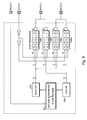
- the memory access is controlled by the Interrupt Manager 1910 , which communicates with the memory access control block via bus 1922 .
- the memory access control block communicates with the memory array 1902 through bidirectional bus 1912 .
- An RFID interface 1904 communicates with memory access control block 1908 via bidirectional bus 1914 , and with interrupt manager 1910 through bus 1916 .
- the secondary interface 1906 communicates with memory access control 1908 via bidirectional bus 1918 , and with interrupt manager 1910 through bus 1920 .
- One or the other of interfaces 1904 and 1906 must be the interrupt master, and have initial control of the memory 1902 . Upon a proper command, that interface can relinquish control and allow the other to take over. When the secondary interface is finished, it signals to the interrupt manager to relinquish the memory busses, and allows the primary interface to have control once again.
- a tag or RFID chip enters the field at step 2004 .
- the reader identifies the tag or RFID chip.
- optional tag operations are performed.
- a first trigger address is written.
- the question is asked if this is a first write at that location. If the answer is yes, the write data from the command is placed in a local register and the method continues at step 2016 . If the answer is no, optional tag operations are performed at step 2016 .
- a second trigger address is stored. At decision block 2020 , the question is asked if this is a first write at that location.
- the write data from the command is placed in a second local register and the method continues at step 2024 .
- the data in the second register is XORed with the first trigger data.
- the result of the XOR operation is compared to the value 1234 . If it is no, then normal tag operations are continued at step 2026 . If the answer at decision block 2020 is no, then operations are also continued at step 2026 . If the answer at decision block 2028 is yes, then an interrupt signal is sent to the serial port chip select, and RFID reception is blocked at step 2030 .
- the serial behavior of the microcontroller in the embedded application is shown in flow chart 2001 .
- the microcontroller is interrupted with the previously described rising edge on the chip select pin.
- the microcontroller acknowledges the interrupt.
- the memory in the RFID chip is read or written to as required.
- Decision block 2040 shows that these memory interactions may be a single or multiple operations before the session is finished. If no, then the memory is read from or written to as required. If yes, the method is continued at step 2042 , wherein an Interrupt End OpCode is sent.
- Flow chart 2002 again describes the operations pertaining to the RFID tag or integrated circuit.
- the interrupt is cleared, and at step 2046 RFID reception is again enabled.
- the memory access control system of the present invention does not have a sophisticated means of coordinating access to the memory between the two different interfaces. Instead, the RFID side is chosen to be the master, which controls all accesses. In the present invention, the secondary serial interface is told when it can access the memory by the RFID master.
- the interrupt method of the present invention is used to wake up the external device which communicates via the serial interface.
- An acknowledge sequence is used to assure reception of the interrupt and lock out the RFID while the serial interface is in control of the memory. This prevents a case where the RFID alone sets the interrupt condition, but the serial interface never responds, and the RFID is forever locked out. Instead, the lockout is under control of the serial interface, and ensures that there cannot be a case where the two interfaces fight for access to the memory.
- an Interrupt End op-code is used to re-allow the RFID to have access to the memory as well as blocking further serial access until the next interrupt cycle.
- the memory access control block is essentially a set of multiplexers.
- the RFID and the Serial interfaces both provide Address, Data and Select controls. Normally, the multiplexers steer the RFID controls to the memory. During an interrupt session, the multiplexers are uniformly switched to the Serial controls and the RFID controls are blocked. If the memory is in the middle of an access cycle, there is a feedback mechanism from the FRAM memory which does not allow this switch to occur before the access is complete.
- the second advantage of this method according to the present invention is that it allows the RFID to communicate directly with the serial interface at the time of its choosing in a closed loop. That is, since it controls the interrupt, it can initiate the activity of the serial interface. Without an interrupt, the serial interface would interact with the memory on its own cadence, and the RFID interface would have to continually check the status.
Abstract
Description
Claims (22)
Priority Applications (3)
| Application Number | Priority Date | Filing Date | Title |
|---|---|---|---|
| US12/833,845 US8957763B2 (en) | 2010-07-09 | 2010-07-09 | RFID access method using an indirect memory pointer |
| US12/833,861 US8723654B2 (en) | 2010-07-09 | 2010-07-09 | Interrupt generation and acknowledgment for RFID |
| CN201110193698.XA CN102314618B (en) | 2010-07-09 | 2011-07-07 | There is RFID interface and the RFID circuit of secondary interface and interrupt method thereof |
Applications Claiming Priority (1)
| Application Number | Priority Date | Filing Date | Title |
|---|---|---|---|
| US12/833,861 US8723654B2 (en) | 2010-07-09 | 2010-07-09 | Interrupt generation and acknowledgment for RFID |
Publications (2)
| Publication Number | Publication Date |
|---|---|
| US20120007723A1 US20120007723A1 (en) | 2012-01-12 |
| US8723654B2 true US8723654B2 (en) | 2014-05-13 |
Family
ID=45427765
Family Applications (1)
| Application Number | Title | Priority Date | Filing Date |
|---|---|---|---|
| US12/833,861 Active 2031-09-20 US8723654B2 (en) | 2010-07-09 | 2010-07-09 | Interrupt generation and acknowledgment for RFID |
Country Status (2)
| Country | Link |
|---|---|
| US (1) | US8723654B2 (en) |
| CN (1) | CN102314618B (en) |
Families Citing this family (8)
| Publication number | Priority date | Publication date | Assignee | Title |
|---|---|---|---|---|
| US9092582B2 (en) | 2010-07-09 | 2015-07-28 | Cypress Semiconductor Corporation | Low power, low pin count interface for an RFID transponder |
| US9846664B2 (en) | 2010-07-09 | 2017-12-19 | Cypress Semiconductor Corporation | RFID interface and interrupt |
| US9496927B1 (en) | 2013-01-21 | 2016-11-15 | Google Inc. | Interrupt based near field communication (NFC) pairing |
| US9520007B2 (en) | 2014-05-05 | 2016-12-13 | James C. Stippich | Remotely operable lockout system |
| WO2015195475A1 (en) * | 2014-06-17 | 2015-12-23 | Cypress Semiconductor Corporation | Rfid interface and interrupt |
| US9798909B2 (en) * | 2014-11-24 | 2017-10-24 | Cypress Semiconductor Corporation | Integrated circuit to convert no-wire signals to one-wire signals |
| CN113988094A (en) * | 2020-07-27 | 2022-01-28 | 意法半导体(格勒诺布尔2)公司 | Contactless transponder and method |
| FR3112877B1 (en) * | 2020-07-27 | 2022-07-15 | St Microelectronics Grenoble 2 | CONTACTLESS TRANSPONDER |
Citations (142)
| Publication number | Priority date | Publication date | Assignee | Title |
|---|---|---|---|---|
| US3184660A (en) | 1961-08-22 | 1965-05-18 | Sprague Electric Co | Ceramic capacitor |
| US3569802A (en) | 1967-09-20 | 1971-03-09 | Siemens Ag | Dielectric capacitors with inner barrier layers and low temperature dependence |
| US3579063A (en) | 1968-03-25 | 1971-05-18 | Matsushita Electric Ind Co Ltd | Thin film capacitor |
| US3819990A (en) | 1971-12-29 | 1974-06-25 | Matsushita Electric Ind Co Ltd | Thin-film capacitor and method for the fabrication thereof |
| US4141022A (en) | 1977-09-12 | 1979-02-20 | Signetics Corporation | Refractory metal contacts for IGFETS |
| US4149301A (en) | 1977-07-25 | 1979-04-17 | Ferrosil Corporation | Monolithic semiconductor integrated circuit-ferroelectric memory drive |
| US4636908A (en) | 1983-01-31 | 1987-01-13 | Nippon Soda Co., Ltd. | Thin-film dielectric and process for its production |
| US4675715A (en) | 1982-12-09 | 1987-06-23 | American Telephone And Telegraph Company, At&T Bell Laboratories | Semiconductor integrated circuit vertical geometry impedance element |
| US4700457A (en) | 1985-03-29 | 1987-10-20 | Mitsubishi Denki Kabushiki Kaisha | Method of making multilayer capacitor memory device |
| US4707897A (en) | 1976-02-17 | 1987-11-24 | Ramtron Corporation | Monolithic semiconductor integrated circuit ferroelectric memory device, and methods of fabricating and utilizing same |
| US4757028A (en) | 1985-10-07 | 1988-07-12 | Agency Of Industrial Science And Technology | Process for preparing a silicon carbide device |
| US4759823A (en) | 1987-06-02 | 1988-07-26 | Krysalis Corporation | Method for patterning PLZT thin films |
| US4809225A (en) | 1987-07-02 | 1989-02-28 | Ramtron Corporation | Memory cell with volatile and non-volatile portions having ferroelectric capacitors |
| US4811078A (en) | 1985-05-01 | 1989-03-07 | Texas Instruments Incorporated | Integrated circuit device and process with tin capacitors |
| US4851895A (en) | 1985-05-06 | 1989-07-25 | American Telephone And Telegraph Company, At&T Bell Laboratories | Metallization for integrated devices |
| US4853893A (en) | 1987-07-02 | 1989-08-01 | Ramtron Corporation | Data storage device and method of using a ferroelectric capacitance divider |
| US4860254A (en) | 1986-01-31 | 1989-08-22 | Bayer Aktiengesellschaft | Non-volatile electronic memory |
| US4873644A (en) | 1987-09-16 | 1989-10-10 | Kubota, Ltd. | Guide system for a working machine having a product identifying system |
| US4873664A (en) | 1987-02-12 | 1989-10-10 | Ramtron Corporation | Self restoring ferroelectric memory |
| US4888733A (en) | 1988-09-12 | 1989-12-19 | Ramtron Corporation | Non-volatile memory cell and sensing method |
| US4893272A (en) | 1988-04-22 | 1990-01-09 | Ramtron Corporation | Ferroelectric retention method |
| US4910708A (en) | 1987-07-02 | 1990-03-20 | Ramtron Corporation | Dram with programmable capacitance divider |
| US4914627A (en) | 1987-07-02 | 1990-04-03 | Ramtron Corporation | One transistor memory cell with programmable capacitance divider |
| US4918654A (en) | 1987-07-02 | 1990-04-17 | Ramtron Corporation | SRAM with programmable capacitance divider |
| US4937650A (en) | 1985-11-29 | 1990-06-26 | Hitachi, Ltd. | Semiconductor capacitor device with dual dielectric |
| US4959745A (en) | 1988-03-04 | 1990-09-25 | Kabushiki Kaisha Toshiba | Capacitor and method for producing the same |
| US4982309A (en) | 1989-07-17 | 1991-01-01 | National Semiconductor Corporation | Electrodes for electrical ceramic oxide devices |
| US5003428A (en) | 1989-07-17 | 1991-03-26 | National Semiconductor Corporation | Electrodes for ceramic oxide capacitors |
| US5005102A (en) | 1989-06-20 | 1991-04-02 | Ramtron Corporation | Multilayer electrodes for integrated circuit capacitors |
| US5024964A (en) | 1970-09-28 | 1991-06-18 | Ramtron Corporation | Method of making ferroelectric memory devices |
| US5031144A (en) | 1990-02-28 | 1991-07-09 | Hughes Aircraft Company | Ferroelectric memory with non-destructive readout including grid electrode between top and bottom electrodes |
| US5036382A (en) | 1989-02-22 | 1991-07-30 | Yamaha Corporation | Semiconductor device having a multi-level wiring structure |
| US5040046A (en) | 1990-10-09 | 1991-08-13 | Micron Technology, Inc. | Process for forming highly conformal dielectric coatings in the manufacture of integrated circuits and product produced thereby |
| US5043049A (en) | 1989-01-26 | 1991-08-27 | Seiko Epson Corporation | Methods of forming ferroelectric thin films |
| US5046043A (en) | 1987-10-08 | 1991-09-03 | National Semiconductor Corporation | Ferroelectric capacitor and memory cell including barrier and isolation layers |
| US5070036A (en) | 1989-01-04 | 1991-12-03 | Quality Microcircuits Corporation | Process for contacting and interconnecting semiconductor devices within an integrated circuit |
| US5099305A (en) | 1989-02-08 | 1992-03-24 | Seiko Epson Corporation | Platinum capacitor mos memory having lattice matched pzt |
| EP0485086A1 (en) | 1990-10-31 | 1992-05-13 | AT&T Corp. | Dielectric layers for integrated circuits |
| US5119154A (en) | 1990-12-03 | 1992-06-02 | Micron Technology, Inc. | Ferroelectric capacitor and method for forming local interconnect |
| US5122477A (en) | 1990-03-16 | 1992-06-16 | U.S. Philips Corporation | Method of manufacturing a semiconductor device comprising capacitors which form memory elements and comprise a ferroelectric dielectric material having multilayer lower and upper electrodes |
| US5124014A (en) | 1990-02-27 | 1992-06-23 | At&T Bell Laboratories | Method of forming oxide layers by bias ECR plasma deposition |
| US5139971A (en) | 1991-06-07 | 1992-08-18 | Intel Corporation | Anneal to decrease moisture absorbance of intermetal dielectrics |
| US5142437A (en) | 1991-06-13 | 1992-08-25 | Ramtron Corporation | Conducting electrode layers for ferroelectric capacitors in integrated circuits and method |
| US5146299A (en) | 1990-03-02 | 1992-09-08 | Westinghouse Electric Corp. | Ferroelectric thin film material, method of deposition, and devices using same |
| US5155573A (en) | 1989-12-25 | 1992-10-13 | Kabushiki Kaisha Toshiba | Ferroelectric capacitor and a semiconductor device having the same |
| US5170242A (en) | 1989-12-04 | 1992-12-08 | Ramtron Corporation | Reaction barrier for a multilayer structure in an integrated circuit |
| US5189503A (en) | 1988-03-04 | 1993-02-23 | Kabushiki Kaisha Toshiba | High dielectric capacitor having low current leakage |
| US5191510A (en) | 1992-04-29 | 1993-03-02 | Ramtron International Corporation | Use of palladium as an adhesion layer and as an electrode in ferroelectric memory devices |
| US5192704A (en) | 1989-06-30 | 1993-03-09 | Texas Instruments Incorporated | Method and apparatus for a filament channel pass gate ferroelectric capacitor memory cell |
| US5206788A (en) | 1991-12-12 | 1993-04-27 | Ramtron Corporation | Series ferroelectric capacitor structure for monolithic integrated circuits and method |
| US5212620A (en) | 1992-03-03 | 1993-05-18 | Radiant Technologies | Method for isolating SiO2 layers from PZT, PLZT, and platinum layers |
| US5216572A (en) | 1992-03-19 | 1993-06-01 | Ramtron International Corporation | Structure and method for increasing the dielectric constant of integrated ferroelectric capacitors |
| US5227855A (en) | 1990-01-24 | 1993-07-13 | Kabushiki Kaisha Toshiba | Semiconductor memory device having a ferroelectric substance as a memory element |
| US5229309A (en) | 1990-06-01 | 1993-07-20 | Ramtron International Corporation | Method of manufacturing semiconductor device using a ferroelectric film over a source region |
| US5231058A (en) | 1989-12-27 | 1993-07-27 | Semiconductor Process Laboratory Co. Ltd. | Process for forming cvd film and semiconductor device |
| DE4107165C2 (en) | 1990-04-13 | 1993-08-12 | Mitsubishi Denki K.K., Tokio/Tokyo, Jp | |
| US5266355A (en) | 1992-06-18 | 1993-11-30 | Eastman Kodak Company | Chemical vapor deposition of metal oxide films |
| US5271955A (en) | 1992-04-06 | 1993-12-21 | Motorola, Inc. | Method for making a semiconductor device having an anhydrous ferroelectric thin film |
| US5273927A (en) | 1990-12-03 | 1993-12-28 | Micron Technology, Inc. | Method of making a ferroelectric capacitor and forming local interconnect |
| US5286681A (en) | 1991-06-20 | 1994-02-15 | Canon Sales Co., Inc. | Method for manufacturing semiconductor device having a self-planarizing film |
| US5293510A (en) | 1990-04-24 | 1994-03-08 | Ramtron International Corporation | Semiconductor device with ferroelectric and method of manufacturing the same |
| US5293075A (en) | 1991-09-03 | 1994-03-08 | Sharp Kabushiki Kaisha | Semiconductor device with PZT/PLZT film and lead-containing electrode |
| US5303186A (en) | 1991-12-26 | 1994-04-12 | Sharp Kabushiki Kaisha | Semiconductor memory and process for manufacturing the same |
| US5307305A (en) | 1991-12-04 | 1994-04-26 | Rohm Co., Ltd. | Semiconductor device having field effect transistor using ferroelectric film as gate insulation film |
| US5319246A (en) | 1989-11-30 | 1994-06-07 | Mitsubishi Denki Kabushiki Kaisha | Semiconductor device having multi-layer film structure |
| US5335138A (en) | 1993-02-12 | 1994-08-02 | Micron Semiconductor, Inc. | High dielectric constant capacitor and method of manufacture |
| US5334554A (en) | 1992-01-24 | 1994-08-02 | Taiwan Semiconductor Manufacturing Co., Ltd. | Nitrogen plasma treatment to prevent field device leakage in VLSI processing |
| US5350705A (en) | 1992-08-25 | 1994-09-27 | National Semiconductor Corporation | Ferroelectric memory cell arrangement having a split capacitor plate structure |
| US5371700A (en) | 1992-10-19 | 1994-12-06 | Sharp Kabushiki Kaisha | Semiconductor memory device with covered sidewall spacers |
| US5375085A (en) | 1992-09-30 | 1994-12-20 | Texas Instruments Incorporated | Three-dimensional ferroelectric integrated circuit without insulation layer between memory layers |
| US5376590A (en) | 1992-01-20 | 1994-12-27 | Nippon Telegraph And Telephone Corporation | Semiconductor device and method of fabricating the same |
| US5381364A (en) | 1993-06-24 | 1995-01-10 | Ramtron International Corporation | Ferroelectric-based RAM sensing scheme including bit-line capacitance isolation |
| US5383150A (en) | 1993-01-25 | 1995-01-17 | Hitachi, Ltd. | Semiconductor memory device |
| US5382817A (en) | 1992-02-20 | 1995-01-17 | Mitsubishi Denki Kabushiki Kaisha | Semiconductor device having a ferroelectric capacitor with a planarized lower electrode |
| US5390143A (en) | 1993-05-17 | 1995-02-14 | Micron Semiconductor, Inc. | Non-volatile static memory devices and operational methods |
| US5396095A (en) | 1991-05-08 | 1995-03-07 | U.S. Philips Corporation | Method of manufacturing a semiconductor device comprising a capacitor with a ferroelectric dielectric, and semiconductor device comprising such a capacitor |
| US5395095A (en) | 1991-10-30 | 1995-03-07 | Paul Wurth S.A. | Combined machine for opening and plugging a taphole in a shaft furnace |
| US5397446A (en) | 1992-07-06 | 1995-03-14 | Sharp Kabushiki Kaisha | Method of forming a ferroelectric film |
| US5400275A (en) | 1990-06-08 | 1995-03-21 | Kabushiki Kaisha Toshiba | Semiconductor memory device using ferroelectric capacitor and having only one sense amplifier selected |
| US5416736A (en) | 1992-07-28 | 1995-05-16 | Motorola, Inc. | Vertical field-effect transistor and a semiconductor memory cell having the transistor |
| US5416735A (en) | 1991-07-02 | 1995-05-16 | Sharp Kabushiki Kaisha | Non-volatile random access memory with ferroelectric capacitor |
| EP0642167A3 (en) | 1993-08-05 | 1995-06-28 | Matsushita Electronics Corp | Semiconductor device having capacitor and manufacturing method thereof. |
| US5438023A (en) | 1994-03-11 | 1995-08-01 | Ramtron International Corporation | Passivation method and structure for a ferroelectric integrated circuit using hard ceramic materials or the like |
| US5440173A (en) | 1993-09-17 | 1995-08-08 | Radiant Technologies | High-temperature electrical contact for making contact to ceramic materials and improved circuit element using the same |
| US5459353A (en) | 1991-02-12 | 1995-10-17 | Matsushita Electronics Corporation | Semiconductor device including interlayer dielectric film layers and conductive film layers |
| US5466629A (en) | 1992-07-23 | 1995-11-14 | Symetrix Corporation | Process for fabricating ferroelectric integrated circuit |
| US5479316A (en) | 1993-08-24 | 1995-12-26 | Analog Devices, Inc. | Integrated circuit metal-oxide-metal capacitor and method of making same |
| US5481490A (en) | 1993-10-12 | 1996-01-02 | Olympus Optical Co., Ltd. | Ferroelectric memory |
| US5495439A (en) | 1993-09-27 | 1996-02-27 | Mitsubishi Denki Kabushiki Kaisha | Semiconductor memory device having SOI structure and manufacturing method thereof |
| US5495117A (en) | 1991-05-29 | 1996-02-27 | Ramtron International Corporation | Stacked ferroelectric memory cell |
| US5502321A (en) | 1993-11-08 | 1996-03-26 | Sharp Kabushiki Kaisha | Flash memory having inclined channel |
| US5506748A (en) | 1991-09-20 | 1996-04-09 | Rohm Co., Ltd. | Capacitor for semiconductor integrated circuit |
| US5523595A (en) | 1990-08-21 | 1996-06-04 | Ramtron International Corporation | Semiconductor device having a transistor, a ferroelectric capacitor and a hydrogen barrier film |
| US5525528A (en) | 1994-02-23 | 1996-06-11 | Ramtron International Corporation | Ferroelectric capacitor renewal method |
| US5530668A (en) | 1995-04-12 | 1996-06-25 | Ramtron International Corporation | Ferroelectric memory sensing scheme using bit lines precharged to a logic one voltage |
| US5532953A (en) | 1995-03-29 | 1996-07-02 | Ramtron International Corporation | Ferroelectric memory sensing method using distinct read and write voltages |
| US5559052A (en) | 1994-12-29 | 1996-09-24 | Lucent Technologies Inc. | Integrated circuit fabrication with interlevel dielectric |
| US5583068A (en) | 1993-08-02 | 1996-12-10 | Motorola, Inc. | Process for forming a capacitor having a metal-oxide dielectric |
| US5608725A (en) | 1995-01-26 | 1997-03-04 | Motorola, Inc. | Method and apparatus of a communications system having a DMT infrastructure |
| US5612238A (en) | 1993-12-28 | 1997-03-18 | Nippon Steel Corporation | Method of manufacturing first and second memory cell arrays with a capacitor and a nonvolatile memory cell |
| US5621681A (en) | 1995-03-22 | 1997-04-15 | Samsung Electronics Co., Ltd. | Device and manufacturing method for a ferroelectric memory |
| US5638319A (en) | 1995-06-05 | 1997-06-10 | Sharp Kabushiki Kaisha | Non-volatile random access memory and fabrication method thereof |
| US5679969A (en) | 1995-03-17 | 1997-10-21 | Radiant Technologies, Inc. | Ferroelectric based capacitor for use in memory systems and method for fabricating the same |
| US5716875A (en) | 1996-03-01 | 1998-02-10 | Motorola, Inc. | Method for making a ferroelectric device |
| US5731608A (en) | 1997-03-07 | 1998-03-24 | Sharp Microelectronics Technology, Inc. | One transistor ferroelectric memory cell and method of making the same |
| US5750419A (en) | 1997-02-24 | 1998-05-12 | Motorola, Inc. | Process for forming a semiconductor device having a ferroelectric capacitor |
| US5789303A (en) | 1994-11-28 | 1998-08-04 | Northern Telecom Limited | Method of adding on chip capacitors to an integrated circuit |
| US5801415A (en) | 1996-05-16 | 1998-09-01 | Taiwan Semiconductor Manufacturing Company Ltd. | Non-volatile-memory cell for electrically programmable read only memory having a trench-like coupling capacitors |
| US5838605A (en) | 1996-03-20 | 1998-11-17 | Ramtron International Corporation | Iridium oxide local interconnect |
| US5851844A (en) | 1996-11-07 | 1998-12-22 | Motorola, Inc. | Ferroelectric semiconductor device and method of manufacture |
| US5858851A (en) | 1996-03-19 | 1999-01-12 | Sharp Kabushiki Kaisha | Manufacturing method of electrode |
| US5866926A (en) | 1990-09-28 | 1999-02-02 | Ramtron International Corporation | Ferroelectric memory device with capacitor electrode in direct contact with source region |
| US5890199A (en) | 1996-10-21 | 1999-03-30 | Ramtron International Corporation | Data processor incorporating a ferroelectric memory array selectably configurable as read/write and read only memory |
| US5902131A (en) | 1997-05-09 | 1999-05-11 | Ramtron International Corporation | Dual-level metalization method for integrated circuit ferroelectric devices |
| US5909624A (en) | 1994-02-10 | 1999-06-01 | Ramtron International Corporation | Method of making integration of high value capacitor with ferroelectric memory |
| US5953619A (en) | 1997-08-06 | 1999-09-14 | Fujitsu Limited | Semiconductor device with perovskite capacitor and its manufacture method |
| US5960279A (en) | 1996-08-27 | 1999-09-28 | Mosel Vitellic Incorporated | Method of fabricating a capacitor on a rugged stacked oxide layer |
| US5960252A (en) | 1996-05-14 | 1999-09-28 | Nec Corporation | Method for manufacturing a semiconductor memory device having a ferroelectric capacitor |
| US5963466A (en) | 1998-04-13 | 1999-10-05 | Radiant Technologies, Inc. | Ferroelectric memory having a common plate electrode |
| US6010969A (en) | 1996-10-02 | 2000-01-04 | Micron Technology, Inc. | Method of depositing films on semiconductor devices by using carboxylate complexes |
| US6020233A (en) | 1997-06-30 | 2000-02-01 | Hyundai Electronics Industries Co., Ltd. | Ferroelectric memory device guaranteeing electrical interconnection between lower capacitor electrode and contact plug and method for fabricating the same |
| US6051858A (en) | 1996-07-26 | 2000-04-18 | Symetrix Corporation | Ferroelectric/high dielectric constant integrated circuit and method of fabricating same |
| US6097622A (en) * | 1996-06-03 | 2000-08-01 | Kabushiki Kaisha Toshiba | Ferroelectric memory used for the RFID system, method for driving the same, semiconductor chip and ID card |
| US6140173A (en) | 1994-10-04 | 2000-10-31 | U.S. Philips Corporation | Method of manufacturing a semiconductor device comprising a ferroelectric memory element |
| US6172386B1 (en) | 1998-06-20 | 2001-01-09 | Samsung Electronics Co., Ltd. | Ferroelectric memory device |
| US6218197B1 (en) | 1999-02-07 | 2001-04-17 | Nec Corporation | Embedded LSI having a FeRAM section and a logic circuit section |
| US6281023B2 (en) | 1996-08-20 | 2001-08-28 | Ramtron International Corporation | Completely encapsulated top electrode of a ferroelectric capacitor using a lead-enhanced encapsulation layer |
| US6281534B1 (en) | 1998-10-13 | 2001-08-28 | Symetrix Corporation | Low imprint ferroelectric material for long retention memory and method of making the same |
| EP0469934B1 (en) | 1990-08-03 | 2001-12-12 | Hitachi, Ltd. | Semiconductor memory device and method of operation thereof |
| US6498741B2 (en) | 1998-12-22 | 2002-12-24 | Kabushiki Kaisha Toshiba | Semiconductor memory device |
| US20050088285A1 (en) * | 2003-10-28 | 2005-04-28 | Samsung Electronics Co., Ltd. | Mobile communication terminal with RFID function and RFID programming method in the same |
| US6901494B2 (en) | 2000-12-27 | 2005-05-31 | Intel Corporation | Memory control translators |
| EP0917204B1 (en) | 1997-11-13 | 2007-01-24 | Matsushita Electric Industrial Co., Ltd. | Interconnection between MOS transistor and capacitor |
| US20080143487A1 (en) | 2006-12-19 | 2008-06-19 | Broadcom Corporation | System and method for enabling interrupts for rfid tags |
| US7405660B2 (en) | 2005-03-24 | 2008-07-29 | Impinj, Inc. | Error recovery in RFID reader systems |
| US7475273B2 (en) | 2001-11-21 | 2009-01-06 | Interdigital Technology Corporation | Hybrid parallel/serial bus interface |
| US7484662B2 (en) | 2004-04-22 | 2009-02-03 | Sensitech Inc. | Recording of location event information in RFID tags |
| US7538678B2 (en) | 2005-12-09 | 2009-05-26 | Electronics And Telecommunications Research Institute | Data storing apparatus and method for RFID tags with sensors |
| US20090276089A1 (en) | 2008-04-07 | 2009-11-05 | Julie Robin Bartholomew | Apparatus for dispensing luggage recognition labels and methods for use |
| US7652637B2 (en) | 2005-07-22 | 2010-01-26 | Brother Kogyo Kabushiki Kaisha | Antenna, and radio-frequency identification tag |
| US7661010B2 (en) | 2006-05-31 | 2010-02-09 | Mosaid Technologies Incorporated | Apparatus and method for interfacing to a memory |
| US7742348B2 (en) | 2006-08-07 | 2010-06-22 | Symbol Technologies, Inc. | Concatenated pointers for radio frequency identification tags |
Family Cites Families (2)
| Publication number | Priority date | Publication date | Assignee | Title |
|---|---|---|---|---|
| KR100766607B1 (en) * | 2006-07-28 | 2007-10-12 | 주식회사 케이티프리텔 | Smart card unified communication functions of contact type and non-contact type and operation controlling method thereof |
| CN100487728C (en) * | 2006-12-30 | 2009-05-13 | 凤凰微电子(中国)有限公司 | Smart card of supporting high performance computing, large capacity storage and high-speed transmission |
-
2010
- 2010-07-09 US US12/833,861 patent/US8723654B2/en active Active
-
2011
- 2011-07-07 CN CN201110193698.XA patent/CN102314618B/en active Active
Patent Citations (152)
| Publication number | Priority date | Publication date | Assignee | Title |
|---|---|---|---|---|
| US3184660A (en) | 1961-08-22 | 1965-05-18 | Sprague Electric Co | Ceramic capacitor |
| US3569802A (en) | 1967-09-20 | 1971-03-09 | Siemens Ag | Dielectric capacitors with inner barrier layers and low temperature dependence |
| US3579063A (en) | 1968-03-25 | 1971-05-18 | Matsushita Electric Ind Co Ltd | Thin film capacitor |
| US5024964A (en) | 1970-09-28 | 1991-06-18 | Ramtron Corporation | Method of making ferroelectric memory devices |
| US3819990A (en) | 1971-12-29 | 1974-06-25 | Matsushita Electric Ind Co Ltd | Thin-film capacitor and method for the fabrication thereof |
| US4707897A (en) | 1976-02-17 | 1987-11-24 | Ramtron Corporation | Monolithic semiconductor integrated circuit ferroelectric memory device, and methods of fabricating and utilizing same |
| US4149301A (en) | 1977-07-25 | 1979-04-17 | Ferrosil Corporation | Monolithic semiconductor integrated circuit-ferroelectric memory drive |
| US4149302A (en) | 1977-07-25 | 1979-04-17 | Ferrosil Corporation | Monolithic semiconductor integrated circuit ferroelectric memory device |
| US4141022A (en) | 1977-09-12 | 1979-02-20 | Signetics Corporation | Refractory metal contacts for IGFETS |
| US4675715A (en) | 1982-12-09 | 1987-06-23 | American Telephone And Telegraph Company, At&T Bell Laboratories | Semiconductor integrated circuit vertical geometry impedance element |
| US4636908A (en) | 1983-01-31 | 1987-01-13 | Nippon Soda Co., Ltd. | Thin-film dielectric and process for its production |
| US4700457A (en) | 1985-03-29 | 1987-10-20 | Mitsubishi Denki Kabushiki Kaisha | Method of making multilayer capacitor memory device |
| US4811078A (en) | 1985-05-01 | 1989-03-07 | Texas Instruments Incorporated | Integrated circuit device and process with tin capacitors |
| US4851895A (en) | 1985-05-06 | 1989-07-25 | American Telephone And Telegraph Company, At&T Bell Laboratories | Metallization for integrated devices |
| US4757028A (en) | 1985-10-07 | 1988-07-12 | Agency Of Industrial Science And Technology | Process for preparing a silicon carbide device |
| US4937650A (en) | 1985-11-29 | 1990-06-26 | Hitachi, Ltd. | Semiconductor capacitor device with dual dielectric |
| US4860254A (en) | 1986-01-31 | 1989-08-22 | Bayer Aktiengesellschaft | Non-volatile electronic memory |
| US4873664A (en) | 1987-02-12 | 1989-10-10 | Ramtron Corporation | Self restoring ferroelectric memory |
| US4759823A (en) | 1987-06-02 | 1988-07-26 | Krysalis Corporation | Method for patterning PLZT thin films |
| US4853893A (en) | 1987-07-02 | 1989-08-01 | Ramtron Corporation | Data storage device and method of using a ferroelectric capacitance divider |
| US4910708A (en) | 1987-07-02 | 1990-03-20 | Ramtron Corporation | Dram with programmable capacitance divider |
| US4914627A (en) | 1987-07-02 | 1990-04-03 | Ramtron Corporation | One transistor memory cell with programmable capacitance divider |
| US4918654A (en) | 1987-07-02 | 1990-04-17 | Ramtron Corporation | SRAM with programmable capacitance divider |
| US4809225A (en) | 1987-07-02 | 1989-02-28 | Ramtron Corporation | Memory cell with volatile and non-volatile portions having ferroelectric capacitors |
| US4873644A (en) | 1987-09-16 | 1989-10-10 | Kubota, Ltd. | Guide system for a working machine having a product identifying system |
| US5046043A (en) | 1987-10-08 | 1991-09-03 | National Semiconductor Corporation | Ferroelectric capacitor and memory cell including barrier and isolation layers |
| US5536672A (en) | 1987-10-08 | 1996-07-16 | National Semiconductor Corporation | Fabrication of ferroelectric capacitor and memory cell |
| US4959745A (en) | 1988-03-04 | 1990-09-25 | Kabushiki Kaisha Toshiba | Capacitor and method for producing the same |
| US5189503A (en) | 1988-03-04 | 1993-02-23 | Kabushiki Kaisha Toshiba | High dielectric capacitor having low current leakage |
| US4893272A (en) | 1988-04-22 | 1990-01-09 | Ramtron Corporation | Ferroelectric retention method |
| US4888733A (en) | 1988-09-12 | 1989-12-19 | Ramtron Corporation | Non-volatile memory cell and sensing method |
| US5070036A (en) | 1989-01-04 | 1991-12-03 | Quality Microcircuits Corporation | Process for contacting and interconnecting semiconductor devices within an integrated circuit |
| US5043049A (en) | 1989-01-26 | 1991-08-27 | Seiko Epson Corporation | Methods of forming ferroelectric thin films |
| US5099305A (en) | 1989-02-08 | 1992-03-24 | Seiko Epson Corporation | Platinum capacitor mos memory having lattice matched pzt |
| US5036382A (en) | 1989-02-22 | 1991-07-30 | Yamaha Corporation | Semiconductor device having a multi-level wiring structure |
| US5005102A (en) | 1989-06-20 | 1991-04-02 | Ramtron Corporation | Multilayer electrodes for integrated circuit capacitors |
| US5192704A (en) | 1989-06-30 | 1993-03-09 | Texas Instruments Incorporated | Method and apparatus for a filament channel pass gate ferroelectric capacitor memory cell |
| US5003428A (en) | 1989-07-17 | 1991-03-26 | National Semiconductor Corporation | Electrodes for ceramic oxide capacitors |
| US4982309A (en) | 1989-07-17 | 1991-01-01 | National Semiconductor Corporation | Electrodes for electrical ceramic oxide devices |
| US5319246A (en) | 1989-11-30 | 1994-06-07 | Mitsubishi Denki Kabushiki Kaisha | Semiconductor device having multi-layer film structure |
| US5170242A (en) | 1989-12-04 | 1992-12-08 | Ramtron Corporation | Reaction barrier for a multilayer structure in an integrated circuit |
| US5155573A (en) | 1989-12-25 | 1992-10-13 | Kabushiki Kaisha Toshiba | Ferroelectric capacitor and a semiconductor device having the same |
| US5231058A (en) | 1989-12-27 | 1993-07-27 | Semiconductor Process Laboratory Co. Ltd. | Process for forming cvd film and semiconductor device |
| US5227855A (en) | 1990-01-24 | 1993-07-13 | Kabushiki Kaisha Toshiba | Semiconductor memory device having a ferroelectric substance as a memory element |
| US5124014A (en) | 1990-02-27 | 1992-06-23 | At&T Bell Laboratories | Method of forming oxide layers by bias ECR plasma deposition |
| US5031144A (en) | 1990-02-28 | 1991-07-09 | Hughes Aircraft Company | Ferroelectric memory with non-destructive readout including grid electrode between top and bottom electrodes |
| US5146299A (en) | 1990-03-02 | 1992-09-08 | Westinghouse Electric Corp. | Ferroelectric thin film material, method of deposition, and devices using same |
| US5122477A (en) | 1990-03-16 | 1992-06-16 | U.S. Philips Corporation | Method of manufacturing a semiconductor device comprising capacitors which form memory elements and comprise a ferroelectric dielectric material having multilayer lower and upper electrodes |
| DE4107165C2 (en) | 1990-04-13 | 1993-08-12 | Mitsubishi Denki K.K., Tokio/Tokyo, Jp | |
| US5293510A (en) | 1990-04-24 | 1994-03-08 | Ramtron International Corporation | Semiconductor device with ferroelectric and method of manufacturing the same |
| US5229309A (en) | 1990-06-01 | 1993-07-20 | Ramtron International Corporation | Method of manufacturing semiconductor device using a ferroelectric film over a source region |
| US5400275A (en) | 1990-06-08 | 1995-03-21 | Kabushiki Kaisha Toshiba | Semiconductor memory device using ferroelectric capacitor and having only one sense amplifier selected |
| EP0469934B1 (en) | 1990-08-03 | 2001-12-12 | Hitachi, Ltd. | Semiconductor memory device and method of operation thereof |
| US5523595A (en) | 1990-08-21 | 1996-06-04 | Ramtron International Corporation | Semiconductor device having a transistor, a ferroelectric capacitor and a hydrogen barrier film |
| US5866926A (en) | 1990-09-28 | 1999-02-02 | Ramtron International Corporation | Ferroelectric memory device with capacitor electrode in direct contact with source region |
| US5040046A (en) | 1990-10-09 | 1991-08-13 | Micron Technology, Inc. | Process for forming highly conformal dielectric coatings in the manufacture of integrated circuits and product produced thereby |
| EP0485086A1 (en) | 1990-10-31 | 1992-05-13 | AT&T Corp. | Dielectric layers for integrated circuits |
| US5119154A (en) | 1990-12-03 | 1992-06-02 | Micron Technology, Inc. | Ferroelectric capacitor and method for forming local interconnect |
| US5273927A (en) | 1990-12-03 | 1993-12-28 | Micron Technology, Inc. | Method of making a ferroelectric capacitor and forming local interconnect |
| US5459353A (en) | 1991-02-12 | 1995-10-17 | Matsushita Electronics Corporation | Semiconductor device including interlayer dielectric film layers and conductive film layers |
| EP0513894B1 (en) | 1991-05-08 | 1996-08-28 | Koninklijke Philips Electronics N.V. | Method of manufacturing a semiconductor device comprising a capacitor with a ferroelectric dielectric, and semiconductor device comprising such a capacitor |
| US5554559A (en) | 1991-05-08 | 1996-09-10 | U.S. Philips Corporation | Method of manufacturing a semiconductor device having a capacitor with a ferroelectric, dielectric |
| US5396095A (en) | 1991-05-08 | 1995-03-07 | U.S. Philips Corporation | Method of manufacturing a semiconductor device comprising a capacitor with a ferroelectric dielectric, and semiconductor device comprising such a capacitor |
| US5495117A (en) | 1991-05-29 | 1996-02-27 | Ramtron International Corporation | Stacked ferroelectric memory cell |
| US5139971A (en) | 1991-06-07 | 1992-08-18 | Intel Corporation | Anneal to decrease moisture absorbance of intermetal dielectrics |
| US5142437A (en) | 1991-06-13 | 1992-08-25 | Ramtron Corporation | Conducting electrode layers for ferroelectric capacitors in integrated circuits and method |
| US5286681A (en) | 1991-06-20 | 1994-02-15 | Canon Sales Co., Inc. | Method for manufacturing semiconductor device having a self-planarizing film |
| US5416735A (en) | 1991-07-02 | 1995-05-16 | Sharp Kabushiki Kaisha | Non-volatile random access memory with ferroelectric capacitor |
| US5293075A (en) | 1991-09-03 | 1994-03-08 | Sharp Kabushiki Kaisha | Semiconductor device with PZT/PLZT film and lead-containing electrode |
| US5506748A (en) | 1991-09-20 | 1996-04-09 | Rohm Co., Ltd. | Capacitor for semiconductor integrated circuit |
| US5395095A (en) | 1991-10-30 | 1995-03-07 | Paul Wurth S.A. | Combined machine for opening and plugging a taphole in a shaft furnace |
| US5307305A (en) | 1991-12-04 | 1994-04-26 | Rohm Co., Ltd. | Semiconductor device having field effect transistor using ferroelectric film as gate insulation film |
| US5206788A (en) | 1991-12-12 | 1993-04-27 | Ramtron Corporation | Series ferroelectric capacitor structure for monolithic integrated circuits and method |
| US5303186A (en) | 1991-12-26 | 1994-04-12 | Sharp Kabushiki Kaisha | Semiconductor memory and process for manufacturing the same |
| US5376590A (en) | 1992-01-20 | 1994-12-27 | Nippon Telegraph And Telephone Corporation | Semiconductor device and method of fabricating the same |
| US5334554A (en) | 1992-01-24 | 1994-08-02 | Taiwan Semiconductor Manufacturing Co., Ltd. | Nitrogen plasma treatment to prevent field device leakage in VLSI processing |
| US5382817A (en) | 1992-02-20 | 1995-01-17 | Mitsubishi Denki Kabushiki Kaisha | Semiconductor device having a ferroelectric capacitor with a planarized lower electrode |
| US5212620A (en) | 1992-03-03 | 1993-05-18 | Radiant Technologies | Method for isolating SiO2 layers from PZT, PLZT, and platinum layers |
| US5216572A (en) | 1992-03-19 | 1993-06-01 | Ramtron International Corporation | Structure and method for increasing the dielectric constant of integrated ferroelectric capacitors |
| US5271955A (en) | 1992-04-06 | 1993-12-21 | Motorola, Inc. | Method for making a semiconductor device having an anhydrous ferroelectric thin film |
| US5191510A (en) | 1992-04-29 | 1993-03-02 | Ramtron International Corporation | Use of palladium as an adhesion layer and as an electrode in ferroelectric memory devices |
| US5266355A (en) | 1992-06-18 | 1993-11-30 | Eastman Kodak Company | Chemical vapor deposition of metal oxide films |
| US5397446A (en) | 1992-07-06 | 1995-03-14 | Sharp Kabushiki Kaisha | Method of forming a ferroelectric film |
| US5466629A (en) | 1992-07-23 | 1995-11-14 | Symetrix Corporation | Process for fabricating ferroelectric integrated circuit |
| US5416736A (en) | 1992-07-28 | 1995-05-16 | Motorola, Inc. | Vertical field-effect transistor and a semiconductor memory cell having the transistor |
| US5350705A (en) | 1992-08-25 | 1994-09-27 | National Semiconductor Corporation | Ferroelectric memory cell arrangement having a split capacitor plate structure |
| US5375085A (en) | 1992-09-30 | 1994-12-20 | Texas Instruments Incorporated | Three-dimensional ferroelectric integrated circuit without insulation layer between memory layers |
| US5371700A (en) | 1992-10-19 | 1994-12-06 | Sharp Kabushiki Kaisha | Semiconductor memory device with covered sidewall spacers |
| US5383150A (en) | 1993-01-25 | 1995-01-17 | Hitachi, Ltd. | Semiconductor memory device |
| US5335138A (en) | 1993-02-12 | 1994-08-02 | Micron Semiconductor, Inc. | High dielectric constant capacitor and method of manufacture |
| US5390143A (en) | 1993-05-17 | 1995-02-14 | Micron Semiconductor, Inc. | Non-volatile static memory devices and operational methods |
| US5381364A (en) | 1993-06-24 | 1995-01-10 | Ramtron International Corporation | Ferroelectric-based RAM sensing scheme including bit-line capacitance isolation |
| US5696394A (en) | 1993-08-02 | 1997-12-09 | Motorola, Inc. | Capacitor having a metal-oxide dielectric |
| US5583068A (en) | 1993-08-02 | 1996-12-10 | Motorola, Inc. | Process for forming a capacitor having a metal-oxide dielectric |
| EP0642167A3 (en) | 1993-08-05 | 1995-06-28 | Matsushita Electronics Corp | Semiconductor device having capacitor and manufacturing method thereof. |
| US5624864A (en) | 1993-08-05 | 1997-04-29 | Matsushita Electronics Corporation | Semiconductor device having capacitor and manufacturing method thereof |
| US5479316A (en) | 1993-08-24 | 1995-12-26 | Analog Devices, Inc. | Integrated circuit metal-oxide-metal capacitor and method of making same |
| US5440173A (en) | 1993-09-17 | 1995-08-08 | Radiant Technologies | High-temperature electrical contact for making contact to ceramic materials and improved circuit element using the same |
| US5495439A (en) | 1993-09-27 | 1996-02-27 | Mitsubishi Denki Kabushiki Kaisha | Semiconductor memory device having SOI structure and manufacturing method thereof |
| US5481490A (en) | 1993-10-12 | 1996-01-02 | Olympus Optical Co., Ltd. | Ferroelectric memory |
| US5502321A (en) | 1993-11-08 | 1996-03-26 | Sharp Kabushiki Kaisha | Flash memory having inclined channel |
| US5612238A (en) | 1993-12-28 | 1997-03-18 | Nippon Steel Corporation | Method of manufacturing first and second memory cell arrays with a capacitor and a nonvolatile memory cell |
| US5909624A (en) | 1994-02-10 | 1999-06-01 | Ramtron International Corporation | Method of making integration of high value capacitor with ferroelectric memory |
| US5525528A (en) | 1994-02-23 | 1996-06-11 | Ramtron International Corporation | Ferroelectric capacitor renewal method |
| US5578867A (en) | 1994-03-11 | 1996-11-26 | Ramtron International Corporation | Passivation method and structure using hard ceramic materials or the like |
| US5438023A (en) | 1994-03-11 | 1995-08-01 | Ramtron International Corporation | Passivation method and structure for a ferroelectric integrated circuit using hard ceramic materials or the like |
| US6140173A (en) | 1994-10-04 | 2000-10-31 | U.S. Philips Corporation | Method of manufacturing a semiconductor device comprising a ferroelectric memory element |
| US5789303A (en) | 1994-11-28 | 1998-08-04 | Northern Telecom Limited | Method of adding on chip capacitors to an integrated circuit |
| US5559052A (en) | 1994-12-29 | 1996-09-24 | Lucent Technologies Inc. | Integrated circuit fabrication with interlevel dielectric |
| US5608725A (en) | 1995-01-26 | 1997-03-04 | Motorola, Inc. | Method and apparatus of a communications system having a DMT infrastructure |
| US5679969A (en) | 1995-03-17 | 1997-10-21 | Radiant Technologies, Inc. | Ferroelectric based capacitor for use in memory systems and method for fabricating the same |
| US5804850A (en) | 1995-03-17 | 1998-09-08 | Radiant Technologies, Inc. | Ferroelectric based capacitor cell for use in memory systems |
| US5621681A (en) | 1995-03-22 | 1997-04-15 | Samsung Electronics Co., Ltd. | Device and manufacturing method for a ferroelectric memory |
| US5532953A (en) | 1995-03-29 | 1996-07-02 | Ramtron International Corporation | Ferroelectric memory sensing method using distinct read and write voltages |
| US5530668A (en) | 1995-04-12 | 1996-06-25 | Ramtron International Corporation | Ferroelectric memory sensing scheme using bit lines precharged to a logic one voltage |
| US5638319A (en) | 1995-06-05 | 1997-06-10 | Sharp Kabushiki Kaisha | Non-volatile random access memory and fabrication method thereof |
| US5716875A (en) | 1996-03-01 | 1998-02-10 | Motorola, Inc. | Method for making a ferroelectric device |
| US6010927A (en) | 1996-03-01 | 2000-01-04 | Motorola, Inc. | Method for making a ferroelectric device having a tantalum nitride barrier layer |
| US5858851A (en) | 1996-03-19 | 1999-01-12 | Sharp Kabushiki Kaisha | Manufacturing method of electrode |
| US5838605A (en) | 1996-03-20 | 1998-11-17 | Ramtron International Corporation | Iridium oxide local interconnect |
| US5985713A (en) | 1996-03-20 | 1999-11-16 | Ramtron International Corporation | Method of forming iridium oxide local interconnect |
| US5960252A (en) | 1996-05-14 | 1999-09-28 | Nec Corporation | Method for manufacturing a semiconductor memory device having a ferroelectric capacitor |
| US5801415A (en) | 1996-05-16 | 1998-09-01 | Taiwan Semiconductor Manufacturing Company Ltd. | Non-volatile-memory cell for electrically programmable read only memory having a trench-like coupling capacitors |
| US6097622A (en) * | 1996-06-03 | 2000-08-01 | Kabushiki Kaisha Toshiba | Ferroelectric memory used for the RFID system, method for driving the same, semiconductor chip and ID card |
| US6051858A (en) | 1996-07-26 | 2000-04-18 | Symetrix Corporation | Ferroelectric/high dielectric constant integrated circuit and method of fabricating same |
| US6281023B2 (en) | 1996-08-20 | 2001-08-28 | Ramtron International Corporation | Completely encapsulated top electrode of a ferroelectric capacitor using a lead-enhanced encapsulation layer |
| US5960279A (en) | 1996-08-27 | 1999-09-28 | Mosel Vitellic Incorporated | Method of fabricating a capacitor on a rugged stacked oxide layer |
| US6010969A (en) | 1996-10-02 | 2000-01-04 | Micron Technology, Inc. | Method of depositing films on semiconductor devices by using carboxylate complexes |
| US5890199A (en) | 1996-10-21 | 1999-03-30 | Ramtron International Corporation | Data processor incorporating a ferroelectric memory array selectably configurable as read/write and read only memory |
| US5851844A (en) | 1996-11-07 | 1998-12-22 | Motorola, Inc. | Ferroelectric semiconductor device and method of manufacture |
| US5750419A (en) | 1997-02-24 | 1998-05-12 | Motorola, Inc. | Process for forming a semiconductor device having a ferroelectric capacitor |
| US5731608A (en) | 1997-03-07 | 1998-03-24 | Sharp Microelectronics Technology, Inc. | One transistor ferroelectric memory cell and method of making the same |
| US5902131A (en) | 1997-05-09 | 1999-05-11 | Ramtron International Corporation | Dual-level metalization method for integrated circuit ferroelectric devices |
| US6020233A (en) | 1997-06-30 | 2000-02-01 | Hyundai Electronics Industries Co., Ltd. | Ferroelectric memory device guaranteeing electrical interconnection between lower capacitor electrode and contact plug and method for fabricating the same |
| US5953619A (en) | 1997-08-06 | 1999-09-14 | Fujitsu Limited | Semiconductor device with perovskite capacitor and its manufacture method |
| EP0917204B1 (en) | 1997-11-13 | 2007-01-24 | Matsushita Electric Industrial Co., Ltd. | Interconnection between MOS transistor and capacitor |
| US5963466A (en) | 1998-04-13 | 1999-10-05 | Radiant Technologies, Inc. | Ferroelectric memory having a common plate electrode |
| US6172386B1 (en) | 1998-06-20 | 2001-01-09 | Samsung Electronics Co., Ltd. | Ferroelectric memory device |
| US6281534B1 (en) | 1998-10-13 | 2001-08-28 | Symetrix Corporation | Low imprint ferroelectric material for long retention memory and method of making the same |
| US6498741B2 (en) | 1998-12-22 | 2002-12-24 | Kabushiki Kaisha Toshiba | Semiconductor memory device |
| US6218197B1 (en) | 1999-02-07 | 2001-04-17 | Nec Corporation | Embedded LSI having a FeRAM section and a logic circuit section |
| US6901494B2 (en) | 2000-12-27 | 2005-05-31 | Intel Corporation | Memory control translators |
| US7475273B2 (en) | 2001-11-21 | 2009-01-06 | Interdigital Technology Corporation | Hybrid parallel/serial bus interface |
| US20050088285A1 (en) * | 2003-10-28 | 2005-04-28 | Samsung Electronics Co., Ltd. | Mobile communication terminal with RFID function and RFID programming method in the same |
| US7484662B2 (en) | 2004-04-22 | 2009-02-03 | Sensitech Inc. | Recording of location event information in RFID tags |
| US7405660B2 (en) | 2005-03-24 | 2008-07-29 | Impinj, Inc. | Error recovery in RFID reader systems |
| US7652637B2 (en) | 2005-07-22 | 2010-01-26 | Brother Kogyo Kabushiki Kaisha | Antenna, and radio-frequency identification tag |
| US7538678B2 (en) | 2005-12-09 | 2009-05-26 | Electronics And Telecommunications Research Institute | Data storing apparatus and method for RFID tags with sensors |
| US7661010B2 (en) | 2006-05-31 | 2010-02-09 | Mosaid Technologies Incorporated | Apparatus and method for interfacing to a memory |
| US7742348B2 (en) | 2006-08-07 | 2010-06-22 | Symbol Technologies, Inc. | Concatenated pointers for radio frequency identification tags |
| US20080143487A1 (en) | 2006-12-19 | 2008-06-19 | Broadcom Corporation | System and method for enabling interrupts for rfid tags |
| US20090276089A1 (en) | 2008-04-07 | 2009-11-05 | Julie Robin Bartholomew | Apparatus for dispensing luggage recognition labels and methods for use |
Non-Patent Citations (50)
| Title |
|---|
| "Use of Conducting Oxides As A Diffusion Barrier in Shallow Junction Semiconductor Devices," IBM Technical Disclosure Bulletin, vol. 30, No. 8, Jan. 1988, pp. 436-437. |
| C. Ting, "New Sturcture for Contact Metallurgy," IBM Technical Disclosure Bulleting, vol. 25, No. 12, Mar. 1983, pp. 6698-6399. |
| Chapman, S.P., et al., "Tuning PZT DO Fabrication Processes by Optimizing Imprint", abstract, Ninth International Symposium on Integrated Ferroelectrics, Santa Fe, New Mexico, Mar. 3, 1997. |
| Chin-An Chang, Deposition of (100) Au., Ag, Pt, Pb and Fe on (100) Si Using Differential Metal Seed Layers, J. Vac. Sci. Technol. A, vol. 9, No. 1, Jan./Feb. 1991. |
| IBM Technical Disclosure Bulletin, "Low Charging Conformal Phosphorous Silicon Glass Passivation Process," Jun. 6, 1995, p. 367. |
| In Seon Park, et al., "Ultra-thin EBL (Encapsulated Barrier Layer) for Ferroelectric Capacitor," IEEE, 1997, pp. 25.6.1-25.6.4. |
| J. Kudo, et al., "A High Stability Electrode Technology for Stacked SrBi2Ta2O9 Capacitors Applicable to Advanced Ferroelectric Memory," IEEE, pp. 25.4, 1-25.4.4, 1997. |
| J. Scott, "Ferroelectric Memory Applications," IEEE 1989 Ultrasonics Symposium, Oct. 3, 1989. |
| Kim, D., et al., "Effects of Substrate Modification on the Growth and Characteristics of MOCVD PZT", pp. 67-79, Ninth International Symposium on Integrated Ferroelectrics, Santa Fe, New Mexico, Mar. 3, 1997. |
| Kim, D., et al., "MOCVD Grown and Characterization of PZT Thin Films", abstract, Ninth International Symposium on Integrated Ferroelectrics, Santa Fe, New Mexico, Mar. 1997. |
| S.F. Vogel and I.C. Barlow, "Sputtered Plantinum as Substrate for Ferroelectric Film Deposition," J. Vac. Sci. Technol., vol. 10, No. 5, Sep./Oct. 1973. |
| USPTO Advisory Action for for U.S. Appl. No. 09/085,280 dated Aug. 29, 2000; 1 page. |
| USPTO Advisory Action for U.S. Appl. No. 07/867,238 dated Dec. 7, 1993; 12 pages. |
| USPTO Advisory Action for U.S. Appl. No. 08/728,740 dated Aug. 12, 1998; 4 pages. |
| USPTO Final Rejection for U.S. Appl. No. 07/867,238 dated Sep. 29, 1993; 9 pages. |
| USPTO Final Rejection for U.S. Appl. No. 08/166,796 dated Jun. 22, 1994; 10 pages. |
| USPTO Final Rejection for U.S. Appl. No. 08/728,740 dated Jun. 2, 1998; 6 pages. |
| USPTO Final Rejection for U.S. Appl. No. 09/085,280 dated Jun. 20, 2000; 4 pages. |
| USPTO Non Final Office Action for U.S. Appl. No. 09/356,534 dated Jun. 20, 2000; 9 pages. |
| USPTO Non Final Rejection for U.S. Appl. No. 08/166,796 dated Mar. 8, 1994; 9 pages. |
| USPTO Non Final Rejection for U.S. Appl. No. 08/238,802 dated Aug. 26, 1994; 9 pages. |
| USPTO Non Final Rejection for U.S. Appl. No. 08/303,134 dated Nov. 10, 1994; 11 pages. |
| USPTO Non Final Rejection for U.S. Appl. No. 08/828,157 dated Mar. 23, 1999; 11 pages. |
| USPTO Non Final Rejection for U.S. Appl. No. 09/085,280 dated Feb. 28, 2000; 9 pages. |
| USPTO Non Final Rejection for U.S. Appl. No. 09/164,952 dated Aug. 3, 2000; 7 pages. |
| USPTO Non Final Rejection for U.S. Appl. No. 09/283,166 dated Jul. 14, 2000; 7 pages. |
| USPTO Non Final Rejection for U.S. Appl. No. 09/783,496 dated May 13, 2002; 11 pages. |
| USPTO Notice of Allowability for U.S. Appl. No. 09/783,496 dated May 16, 2003; 5 pages. |
| USPTO Notice of Allowance for U.S. Appl. No. 08/238,802 dated Feb. 10, 1995; 9 pages. |
| USPTO Notice of Allowance for U.S. Appl. No. 08/303,134 dated May 16, 1995; 6 pages. |
| USPTO Notice of Allowance for U.S. Appl. No. 08/700,076 dated Feb. 1, 1999; 5 pages. |
| USPTO Notice of Allowance for U.S. Appl. No. 08/728,740 dated Sep. 28, 1998; 3 pages. |
| USPTO Notice of Allowance for U.S. Appl. No. 08/828,157 dated Oct. 6, 1999; 4 pages. |
| USPTO Notice of Allowance for U.S. Appl. No. 09/085,280 dated Dec. 18, 2000; 6 pages. |
| USPTO Notice of Allowance for U.S. Appl. No. 09/164,952 dated Jan. 16, 2001; 6 pages. |
| USPTO Notice of Allowance for U.S. Appl. No. 09/177,392 dated Aug. 8, 2000; 8 pages. |
| USPTO Notice of Allowance for U.S. Appl. No. 09/283,166 dated Feb. 15, 2001; 5 pages. |
| USPTO Notice of Allowance for U.S. Appl. No. 09/356,534 dated Oct. 10, 2000; 5 pages. |
| USPTO Notice of Allowance for U.S. Appl. No. 09/505,106 dated Jul. 27, 2000; 10 pages. |
| USPTO Notice of Allowance for U.S. Appl. No. 09/641,091 dated Oct. 19, 2001; 13 pages. |
| USPTO Notice of Allowance for U.S. Appl. No. 09/783,496 dated Nov. 19, 2002; 10 pages. |
| USPTO Restriction Requirement for U.S. Appl. No. 07/867,238 dated Jun. 11, 1993; 12 pages. |
| USPTO Restriction Requirement for U.S. Appl. No. 08/700,076 dated Nov. 12, 1998; 10 pages. |
| USPTO Restriction Requirement for U.S. Appl. No. 08/728,740 dated Jan. 15, 1998; 5 pages. |
| USPTO Restriction Requirement for U.S. Appl. No. 08/728,740 dated Mar. 19, 1998; 7 pages. |
| USPTO Restriction Requirement for U.S. Appl. No. 08/828,157 dated Jun. 22, 1999; 5 pages. |
| USPTO Restriction Requirement for U.S. Appl. No. 09/164,952 dated Jul. 5, 2000; 4 pages. |
| USPTO Restriction Requirement for U.S. Appl. No. 09/177,392 dated Feb. 24, 2000; 5 pages. |
| USPTO Restriction Requirement for U.S. Appl. No. 09/177,392 dated May 16, 2000; 5 pages. |
| USPTO Restriction Requirement for U.S. Appl. No. 09/641,091 dated Aug. 24, 2001; 4 pages. |
Also Published As
| Publication number | Publication date |
|---|---|
| US20120007723A1 (en) | 2012-01-12 |
| CN102314618A (en) | 2012-01-11 |
| CN102314618B (en) | 2016-09-14 |
Similar Documents
| Publication | Publication Date | Title |
|---|---|---|
| US8686836B2 (en) | Fast block write using an indirect memory pointer | |
| US8723654B2 (en) | Interrupt generation and acknowledgment for RFID | |
| US11789521B2 (en) | Card and host apparatus | |
| KR100375217B1 (en) | Microcontroller incorporating an electrically rewritable non-volatile memory | |
| US6046676A (en) | Self powered electronic memory identification tag with dual communication ports | |
| US8166230B2 (en) | Memory systems and methods of initializing the same | |
| US9870316B2 (en) | Bidirectional counter in a flash memory | |
| US9846664B2 (en) | RFID interface and interrupt | |
| JP2003150574A (en) | Microcomputer | |
| US8957763B2 (en) | RFID access method using an indirect memory pointer | |
| US7069352B2 (en) | Serial peripheral interface and related methods | |
| US9092582B2 (en) | Low power, low pin count interface for an RFID transponder | |
| CN102314581A (en) | Use the RFID access method of indirect memory pointer | |
| WO2015195475A1 (en) | Rfid interface and interrupt | |
| JPH0991267A (en) | Data writer for non-volatile memory | |
| JPH02220189A (en) | Portable ic card terminal equipment | |
| JPH11353437A (en) | Ic card |
Legal Events
| Date | Code | Title | Description |
|---|---|---|---|
| AS | Assignment |
Owner name: RAMTRON INTERNATIONAL CORPORATION, COLORADO Free format text: ASSIGNMENT OF ASSIGNORS INTEREST;ASSIGNORS:WHITAKER, MARK R.;MARENTETTE, LESLIE JOSEPH;SIGNING DATES FROM 20100614 TO 20100630;REEL/FRAME:024668/0460 |
|
| AS | Assignment |
Owner name: CYPRESS SEMICONDUCTOR CORPORATION, CALIFORNIA Free format text: ASSIGNMENT OF ASSIGNORS INTEREST;ASSIGNOR:RAMTRON INTERNATIONAL CORPORATION;REEL/FRAME:029408/0437 Effective date: 20121203 |
|
| STCF | Information on status: patent grant |
Free format text: PATENTED CASE |
|
| AS | Assignment |
Owner name: MORGAN STANLEY SENIOR FUNDING, INC., NEW YORK Free format text: SECURITY INTEREST;ASSIGNORS:CYPRESS SEMICONDUCTOR CORPORATION;SPANSION LLC;REEL/FRAME:035240/0429 Effective date: 20150312 |
|
| MAFP | Maintenance fee payment |
Free format text: PAYMENT OF MAINTENANCE FEE, 4TH YEAR, LARGE ENTITY (ORIGINAL EVENT CODE: M1551) Year of fee payment: 4 |
|
| AS | Assignment |
Owner name: MUFG UNION BANK, N.A., CALIFORNIA Free format text: ASSIGNMENT AND ASSUMPTION OF SECURITY INTEREST IN INTELLECTUAL PROPERTY;ASSIGNOR:MORGAN STANLEY SENIOR FUNDING, INC.;REEL/FRAME:050896/0366 Effective date: 20190731 |
|
| AS | Assignment |
Owner name: MORGAN STANLEY SENIOR FUNDING, INC., NEW YORK Free format text: CORRECTIVE ASSIGNMENT TO CORRECT THE 8647899 PREVIOUSLY RECORDED ON REEL 035240 FRAME 0429. ASSIGNOR(S) HEREBY CONFIRMS THE SECURITY INTERST;ASSIGNORS:CYPRESS SEMICONDUCTOR CORPORATION;SPANSION LLC;REEL/FRAME:058002/0470 Effective date: 20150312 |
|
| MAFP | Maintenance fee payment |
Free format text: PAYMENT OF MAINTENANCE FEE, 8TH YEAR, LARGE ENTITY (ORIGINAL EVENT CODE: M1552); ENTITY STATUS OF PATENT OWNER: LARGE ENTITY Year of fee payment: 8 |
|
| AS | Assignment |
Owner name: SPANSION LLC, CALIFORNIA Free format text: RELEASE BY SECURED PARTY;ASSIGNOR:MUFG UNION BANK, N.A.;REEL/FRAME:059410/0438 Effective date: 20200416 Owner name: CYPRESS SEMICONDUCTOR CORPORATION, CALIFORNIA Free format text: RELEASE BY SECURED PARTY;ASSIGNOR:MUFG UNION BANK, N.A.;REEL/FRAME:059410/0438 Effective date: 20200416 |