US8772101B2 - Methods of forming replacement gate structures on semiconductor devices and the resulting device - Google Patents
Methods of forming replacement gate structures on semiconductor devices and the resulting device Download PDFInfo
- Publication number
- US8772101B2 US8772101B2 US13/671,940 US201213671940A US8772101B2 US 8772101 B2 US8772101 B2 US 8772101B2 US 201213671940 A US201213671940 A US 201213671940A US 8772101 B2 US8772101 B2 US 8772101B2
- Authority
- US
- United States
- Prior art keywords
- sidewall spacers
- gate
- layer
- gate structure
- forming
- Prior art date
- Legal status (The legal status is an assumption and is not a legal conclusion. Google has not performed a legal analysis and makes no representation as to the accuracy of the status listed.)
- Active
Links
- 238000000034 method Methods 0.000 title claims abstract description 119
- 239000004065 semiconductor Substances 0.000 title description 19
- 125000006850 spacer group Chemical group 0.000 claims abstract description 106
- 239000011810 insulating material Substances 0.000 claims abstract description 71
- 230000008569 process Effects 0.000 claims description 71
- 239000000463 material Substances 0.000 claims description 45
- 238000005530 etching Methods 0.000 claims description 32
- 238000009413 insulation Methods 0.000 claims description 24
- VYPSYNLAJGMNEJ-UHFFFAOYSA-N Silicium dioxide Chemical compound O=[Si]=O VYPSYNLAJGMNEJ-UHFFFAOYSA-N 0.000 claims description 19
- 229910052751 metal Inorganic materials 0.000 claims description 14
- 239000002184 metal Substances 0.000 claims description 14
- 229910052581 Si3N4 Inorganic materials 0.000 claims description 13
- HQVNEWCFYHHQES-UHFFFAOYSA-N silicon nitride Chemical compound N12[Si]34N5[Si]62N3[Si]51N64 HQVNEWCFYHHQES-UHFFFAOYSA-N 0.000 claims description 12
- 239000000377 silicon dioxide Substances 0.000 claims description 9
- 235000012239 silicon dioxide Nutrition 0.000 claims description 9
- 229910021420 polycrystalline silicon Inorganic materials 0.000 claims description 7
- 229920005591 polysilicon Polymers 0.000 claims description 7
- 230000009969 flowable effect Effects 0.000 claims description 3
- 229910052582 BN Inorganic materials 0.000 claims description 2
- ZILJFRYKLPPLTO-UHFFFAOYSA-N [C].[B].[Si] Chemical compound [C].[B].[Si] ZILJFRYKLPPLTO-UHFFFAOYSA-N 0.000 claims description 2
- HMDDXIMCDZRSNE-UHFFFAOYSA-N [C].[Si] Chemical compound [C].[Si] HMDDXIMCDZRSNE-UHFFFAOYSA-N 0.000 claims description 2
- 239000000758 substrate Substances 0.000 abstract description 24
- 238000004519 manufacturing process Methods 0.000 description 13
- 239000002253 acid Substances 0.000 description 10
- 239000011295 pitch Substances 0.000 description 10
- 238000012545 processing Methods 0.000 description 9
- 230000015572 biosynthetic process Effects 0.000 description 8
- XUIMIQQOPSSXEZ-UHFFFAOYSA-N Silicon Chemical compound [Si] XUIMIQQOPSSXEZ-UHFFFAOYSA-N 0.000 description 7
- 229910052710 silicon Inorganic materials 0.000 description 7
- 239000010703 silicon Substances 0.000 description 7
- 230000007423 decrease Effects 0.000 description 4
- 230000000694 effects Effects 0.000 description 4
- 238000005229 chemical vapour deposition Methods 0.000 description 3
- 238000010276 construction Methods 0.000 description 3
- 238000000151 deposition Methods 0.000 description 3
- 230000006870 function Effects 0.000 description 3
- 230000009467 reduction Effects 0.000 description 3
- 229910052715 tantalum Inorganic materials 0.000 description 3
- GUVRBAGPIYLISA-UHFFFAOYSA-N tantalum atom Chemical compound [Ta] GUVRBAGPIYLISA-UHFFFAOYSA-N 0.000 description 3
- NRTOMJZYCJJWKI-UHFFFAOYSA-N Titanium nitride Chemical compound [Ti]#N NRTOMJZYCJJWKI-UHFFFAOYSA-N 0.000 description 2
- 229910052782 aluminium Inorganic materials 0.000 description 2
- XAGFODPZIPBFFR-UHFFFAOYSA-N aluminium Chemical compound [Al] XAGFODPZIPBFFR-UHFFFAOYSA-N 0.000 description 2
- 238000000231 atomic layer deposition Methods 0.000 description 2
- 230000008901 benefit Effects 0.000 description 2
- 239000004020 conductor Substances 0.000 description 2
- 230000003247 decreasing effect Effects 0.000 description 2
- 238000013461 design Methods 0.000 description 2
- 238000011161 development Methods 0.000 description 2
- 229910000449 hafnium oxide Inorganic materials 0.000 description 2
- -1 hafnium silicates Chemical class 0.000 description 2
- WIHZLLGSGQNAGK-UHFFFAOYSA-N hafnium(4+);oxygen(2-) Chemical compound [O-2].[O-2].[Hf+4] WIHZLLGSGQNAGK-UHFFFAOYSA-N 0.000 description 2
- 239000007943 implant Substances 0.000 description 2
- 239000012212 insulator Substances 0.000 description 2
- 238000002955 isolation Methods 0.000 description 2
- 238000001465 metallisation Methods 0.000 description 2
- NFFIWVVINABMKP-UHFFFAOYSA-N methylidynetantalum Chemical compound [Ta]#C NFFIWVVINABMKP-UHFFFAOYSA-N 0.000 description 2
- 238000012986 modification Methods 0.000 description 2
- 230000004048 modification Effects 0.000 description 2
- TWNQGVIAIRXVLR-UHFFFAOYSA-N oxo(oxoalumanyloxy)alumane Chemical compound O=[Al]O[Al]=O TWNQGVIAIRXVLR-UHFFFAOYSA-N 0.000 description 2
- RVTZCBVAJQQJTK-UHFFFAOYSA-N oxygen(2-);zirconium(4+) Chemical compound [O-2].[O-2].[Zr+4] RVTZCBVAJQQJTK-UHFFFAOYSA-N 0.000 description 2
- 238000000059 patterning Methods 0.000 description 2
- 238000005498 polishing Methods 0.000 description 2
- 229920003209 poly(hydridosilsesquioxane) Polymers 0.000 description 2
- 239000002210 silicon-based material Substances 0.000 description 2
- 239000000126 substance Substances 0.000 description 2
- 229910003468 tantalcarbide Inorganic materials 0.000 description 2
- 239000010936 titanium Substances 0.000 description 2
- 229910001928 zirconium oxide Inorganic materials 0.000 description 2
- PIGFYZPCRLYGLF-UHFFFAOYSA-N Aluminum nitride Chemical compound [Al]#N PIGFYZPCRLYGLF-UHFFFAOYSA-N 0.000 description 1
- GWEVSGVZZGPLCZ-UHFFFAOYSA-N Titan oxide Chemical compound O=[Ti]=O GWEVSGVZZGPLCZ-UHFFFAOYSA-N 0.000 description 1
- RTAQQCXQSZGOHL-UHFFFAOYSA-N Titanium Chemical compound [Ti] RTAQQCXQSZGOHL-UHFFFAOYSA-N 0.000 description 1
- 230000002411 adverse Effects 0.000 description 1
- UQZIWOQVLUASCR-UHFFFAOYSA-N alumane;titanium Chemical compound [AlH3].[Ti] UQZIWOQVLUASCR-UHFFFAOYSA-N 0.000 description 1
- 229910021417 amorphous silicon Inorganic materials 0.000 description 1
- 238000011982 device technology Methods 0.000 description 1
- 239000002019 doping agent Substances 0.000 description 1
- 239000007772 electrode material Substances 0.000 description 1
- 238000005516 engineering process Methods 0.000 description 1
- 230000005669 field effect Effects 0.000 description 1
- 229910052732 germanium Inorganic materials 0.000 description 1
- GNPVGFCGXDBREM-UHFFFAOYSA-N germanium atom Chemical compound [Ge] GNPVGFCGXDBREM-UHFFFAOYSA-N 0.000 description 1
- 229910052735 hafnium Inorganic materials 0.000 description 1
- CJNBYAVZURUTKZ-UHFFFAOYSA-N hafnium(iv) oxide Chemical compound O=[Hf]=O CJNBYAVZURUTKZ-UHFFFAOYSA-N 0.000 description 1
- 125000001475 halogen functional group Chemical group 0.000 description 1
- 239000012774 insulation material Substances 0.000 description 1
- 238000005468 ion implantation Methods 0.000 description 1
- 229910044991 metal oxide Inorganic materials 0.000 description 1
- 150000004706 metal oxides Chemical class 0.000 description 1
- BPUBBGLMJRNUCC-UHFFFAOYSA-N oxygen(2-);tantalum(5+) Chemical compound [O-2].[O-2].[O-2].[O-2].[O-2].[Ta+5].[Ta+5] BPUBBGLMJRNUCC-UHFFFAOYSA-N 0.000 description 1
- 238000000206 photolithography Methods 0.000 description 1
- 238000011112 process operation Methods 0.000 description 1
- 238000003672 processing method Methods 0.000 description 1
- 230000008439 repair process Effects 0.000 description 1
- 238000000926 separation method Methods 0.000 description 1
- 229910021332 silicide Inorganic materials 0.000 description 1
- FVBUAEGBCNSCDD-UHFFFAOYSA-N silicide(4-) Chemical compound [Si-4] FVBUAEGBCNSCDD-UHFFFAOYSA-N 0.000 description 1
- HWEYZGSCHQNNEH-UHFFFAOYSA-N silicon tantalum Chemical compound [Si].[Ta] HWEYZGSCHQNNEH-UHFFFAOYSA-N 0.000 description 1
- 238000003860 storage Methods 0.000 description 1
- MZLGASXMSKOWSE-UHFFFAOYSA-N tantalum nitride Chemical compound [Ta]#N MZLGASXMSKOWSE-UHFFFAOYSA-N 0.000 description 1
- 229910052719 titanium Inorganic materials 0.000 description 1
- WFKWXMTUELFFGS-UHFFFAOYSA-N tungsten Chemical compound [W] WFKWXMTUELFFGS-UHFFFAOYSA-N 0.000 description 1
- 229910052721 tungsten Inorganic materials 0.000 description 1
- 239000010937 tungsten Substances 0.000 description 1
Images


Classifications
-
- H—ELECTRICITY
- H01—ELECTRIC ELEMENTS
- H01L—SEMICONDUCTOR DEVICES NOT COVERED BY CLASS H10
- H01L29/00—Semiconductor devices adapted for rectifying, amplifying, oscillating or switching, or capacitors or resistors with at least one potential-jump barrier or surface barrier, e.g. PN junction depletion layer or carrier concentration layer; Details of semiconductor bodies or of electrodes thereof ; Multistep manufacturing processes therefor
- H01L29/66—Types of semiconductor device ; Multistep manufacturing processes therefor
- H01L29/66007—Multistep manufacturing processes
- H01L29/66075—Multistep manufacturing processes of devices having semiconductor bodies comprising group 14 or group 13/15 materials
- H01L29/66227—Multistep manufacturing processes of devices having semiconductor bodies comprising group 14 or group 13/15 materials the devices being controllable only by the electric current supplied or the electric potential applied, to an electrode which does not carry the current to be rectified, amplified or switched, e.g. three-terminal devices
- H01L29/66409—Unipolar field-effect transistors
- H01L29/66477—Unipolar field-effect transistors with an insulated gate, i.e. MISFET
- H01L29/66545—Unipolar field-effect transistors with an insulated gate, i.e. MISFET using a dummy, i.e. replacement gate in a process wherein at least a part of the final gate is self aligned to the dummy gate
-
- H—ELECTRICITY
- H01—ELECTRIC ELEMENTS
- H01L—SEMICONDUCTOR DEVICES NOT COVERED BY CLASS H10
- H01L29/00—Semiconductor devices adapted for rectifying, amplifying, oscillating or switching, or capacitors or resistors with at least one potential-jump barrier or surface barrier, e.g. PN junction depletion layer or carrier concentration layer; Details of semiconductor bodies or of electrodes thereof ; Multistep manufacturing processes therefor
- H01L29/66—Types of semiconductor device ; Multistep manufacturing processes therefor
- H01L29/66007—Multistep manufacturing processes
- H01L29/66075—Multistep manufacturing processes of devices having semiconductor bodies comprising group 14 or group 13/15 materials
- H01L29/66227—Multistep manufacturing processes of devices having semiconductor bodies comprising group 14 or group 13/15 materials the devices being controllable only by the electric current supplied or the electric potential applied, to an electrode which does not carry the current to be rectified, amplified or switched, e.g. three-terminal devices
- H01L29/66409—Unipolar field-effect transistors
- H01L29/66477—Unipolar field-effect transistors with an insulated gate, i.e. MISFET
- H01L29/6653—Unipolar field-effect transistors with an insulated gate, i.e. MISFET using the removal of at least part of spacer, e.g. disposable spacer
-
- H—ELECTRICITY
- H01—ELECTRIC ELEMENTS
- H01L—SEMICONDUCTOR DEVICES NOT COVERED BY CLASS H10
- H01L29/00—Semiconductor devices adapted for rectifying, amplifying, oscillating or switching, or capacitors or resistors with at least one potential-jump barrier or surface barrier, e.g. PN junction depletion layer or carrier concentration layer; Details of semiconductor bodies or of electrodes thereof ; Multistep manufacturing processes therefor
- H01L29/66—Types of semiconductor device ; Multistep manufacturing processes therefor
- H01L29/68—Types of semiconductor device ; Multistep manufacturing processes therefor controllable by only the electric current supplied, or only the electric potential applied, to an electrode which does not carry the current to be rectified, amplified or switched
- H01L29/76—Unipolar devices, e.g. field effect transistors
- H01L29/772—Field effect transistors
- H01L29/78—Field effect transistors with field effect produced by an insulated gate
Definitions
- the present disclosure relates to the manufacture of sophisticated semiconductor devices, and, more specifically, to various methods of forming replacement gates structures on semiconductor devices and various semiconductor devices with replacement gates made using such methods.
- a FET is a planar device that typically includes a source region, a drain region, a channel region that is positioned between the source region and the drain region, and a gate electrode positioned above the channel region. Current flow through the FET is controlled by controlling the voltage applied to the gate electrode.
- the gate electrode If there is no voltage applied to the gate electrode, then there is no current flow through the device (ignoring undesirable leakage currents, which are relatively small). However, when an appropriate voltage is applied to the gate electrode, the channel region becomes conductive, and electrical current is permitted to flow between the source region and the drain region through the conductive channel region.
- the channel length of FETs has been significantly decreased, which has resulted in improving the switching speed of FETs.
- decreasing the channel length of a FET also decreases the distance between the source region and the drain region. In some cases, this decrease in the separation between the source and the drain makes it difficult to efficiently inhibit the electrical potential of the source region and the channel from being adversely affected by the electrical potential of the drain. This is sometimes referred to as a so-called short channel effect, wherein the characteristic of the FET as an active switch is degraded.
- a so-called FinFET device has a three-dimensional (3D) structure. More specifically, in a FinFET, a generally vertically positioned fin-shaped active area is formed and a gate electrode encloses both sides and an upper surface of the fin-shaped active area to form a tri-gate structure so as to use a channel having a three-dimensional structure instead of a planar structure.
- an insulating cap layer e.g., silicon nitride, is positioned at the top of the fin and the FinFET device only has a dual-gate structure.
- a channel is formed perpendicular to a surface of the semiconducting substrate so as to reduce the physical size of the semiconductor device. Also, in a FinFET, the junction capacitance at the drain region of the device is greatly reduced, which tends to reduce at least some short channel effects.
- the gate structures of most transistor devices have been comprised of a plurality of silicon-based materials, such as a silicon dioxide and/or silicon oxynitride gate insulation layer, in combination with a polysilicon gate electrode.
- silicon-based materials such as a silicon dioxide and/or silicon oxynitride gate insulation layer
- many newer generation devices employ gate structures that contain alternative materials in an effort to avoid the short channel effects which may be associated with the use of traditional silicon-based materials in reduced channel length transistors.
- gate structures that include a so-called high-k dielectric gate insulation layer and one or more metal layers that function as the gate electrode (HK/MG) have been implemented.
- HK/MG gate electrode
- Such alternative gate structures have been shown to provide significantly enhanced operational characteristics over the heretofore more traditional silicon dioxide/polysilicon gate structure configurations.
- a high-k gate insulation layer may include tantalum oxide (Ta 2 O 5 ), hafnium oxide (HfO 2 ), zirconium oxide (ZrO 2 ), titanium oxide (TiO 2 ), aluminum oxide (Al 2 O 3 ), hafnium silicates (HfSiO x ) and the like.
- one or more non-polysilicon metal gate electrode materials may be used in HK/MG configurations so as to control the work function of the transistor.
- These metal gate electrode materials may include, for example, one or more layers of titanium (Ti), titanium nitride (TiN), titanium-aluminum (TiAl), aluminum (Al), aluminum nitride (AlN), tantalum (Ta), tantalum nitride (TaN), tantalum carbide (TaC), tantalum carbonitride (TaCN), tantalum silicon nitride (TaSiN), tantalum silicide (TaSi) and the like.
- gate last or “replacement gate” technique.
- the replacement gate technique has been employed on both planar and 3D devices, like FinFETs.
- a so-called “dummy” or sacrificial gate structure is initially formed and remains in place as many process operations are performed to form the device, e.g., the formation of doped source/drain regions, performing an anneal process to repair damage to the substrate caused by the ion implantation processes and to activate the implanted dopant materials.
- the sacrificial gate structure is removed to define a gate cavity where the final HK/MG gate structure for the device is formed.
- FIGS. 1A-1K depict one illustrative prior art method for forming an HK/MG replacement gate structure using a replacement gate technique.
- an integrated circuit device 10 is comprised of a plurality of illustrative sacrificial gate structures 13 .
- Each of the sacrificial agate structures 13 is comprised of a sacrificial gate insulation layer 14 , e.g., a layer of silicon dioxide, and a sacrificial gate electrode 15 , e.g., a layer of polysilicon.
- a gate cap layer 17 e.g., a layer of silicon nitride, is positioned above the sacrificial gate electrode 15 .
- a layer of insulating material 18 e.g., a layer of flowable silicon dioxide, has been formed on the device 10 .
- the sacrificial gate structures 13 and the gate cap layers 17 may be formed by forming the various layers of material across the substrate 12 and thereafter patterning the layers of material.
- the sidewall spacers 16 may then be formed by conformably depositing a layer of spacer material and thereafter performing an anisotropic etching process.
- the layer of insulating material 18 may be formed by performing a chemical vapor deposition process.
- FIG. 1B depicts the device 10 after a chemical mechanical polishing (CMP) process has been performed to remove excess portions of the layer of insulating material 18 and to expose the gate cap layer 17 .
- CMP chemical mechanical polishing
- an etching process has been performed to remove a portion of, or recess, the layer of insulating material 18 .
- the etching process is performed such that, after etching, the recessed surface 18 R of the layer of insulating material 18 is positioned below the upper surface 15 S of the sacrificial gate electrode 15 .
- the material selected for the layer of insulating material 18 is typically selected based upon its ability to reliably fill the very small spaces between spacers 16 on adjacent replacement gate structures 13 as shown in FIG.
- a flowable oxide material may be the material selected for the layer of insulating material 18 . While such a material may have good “fill” capabilities, it exhibits relatively poor etch selectivity when subjected to an etching process that will be performed later to remove silicon nitride materials. Thus, an upper portion of the layer of insulating material 18 is removed and replaced with a layer of insulating material that exhibits a better etch selectivity when exposed to an etching process that is performed to remove silicon nitride.
- FIG. 1D depicts the device 10 after a layer of insulating material 20 , e.g., an HDP oxide, has been deposited on the device and after a CMP process has been performed to remove excess amounts of the layer of insulating material 20 .
- the CMP process exposes the cap layers 17 and spacers 16 for further processing.
- an etching process has been performed to remove the gate cap layers 17 and portions of the sidewall spacers 16 . This etching process exposes the sacrificial gate electrodes 15 for further processing.
- FIG. 1D depicts the device 10 after a layer of insulating material 20 , e.g., an HDP oxide, has been deposited on the device and after a CMP process has been performed to remove excess amounts of the layer of insulating material 20 .
- the CMP process exposes the cap layers 17 and spacers 16 for further processing.
- an etching process has been performed to remove the gate cap layers 17 and portions of the sidewall spacers 16 . This etch
- FIG. 1F depicts the device 10 after one or more etching processes have been performed to remove the sacrificial gate electrode 15 and the sacrificial gate insulation layer 14 to thereby define a gate cavity 22 where a replacement gate structure will subsequently be formed.
- the sacrificial gate insulation layer 14 is removed as part of the replacement gate technique, as depicted herein. However, the sacrificial gate insulation layer 14 may not be removed in all applications.
- FIG. 1G depicts the device 10 after schematically depicted replacement gate structures 24 have been formed in the gate cavities 22 . The materials used for such replacement gate structures 24 may vary depending upon the particular application.
- the replacement gate structure 24 is comprised of a high-k gate insulation layer, such as hafnium oxide, and one or more layers of metal.
- the layers of material that comprise the replacement gate structure 24 are sequentially deposited in the gate cavities 22 and one or more CMP processes are performed to remove excess portions of these layers of material to thereby arrive at the replacement gate structures 24 depicted in FIG. 1G , wherein the upper portions of the replacement gate structure 24 are separated from one another by the insulating material 20 .
- the device will typically be subjected to a pre-clean process, usually with HF acid, to insure that all non-desired materials are removed from the surface of the substrate 12 prior to forming the layers of material that will be part of the replacement gate structure 24 .
- a pre-clean process usually with HF acid
- the layer of insulating material 20 does exhibit better etch selectivity than the layer of insulating material 18 when exposed prior to an etching process designed to remove silicon nitride, the layer of insulating material 20 may be severely degraded or substantially consumed when exposed to this pre-clean process that uses HF acid. This becomes problematic as the gate pitch 13 P (see FIG. 1D ) on devices continues to shrink.
- width 20 X (see FIG. 1D ) of the upstanding portions of the layer of insulating material 20 increases as the gate pitch 13 P increases. Conversely, the width 20 X decreases as the gate pitch 13 P decreases. The thinner the width 20 X, the more likely the upstanding portions of the layer of insulating material 20 may be completely consumed during the HF acid pre-clean process.
- FIG. 1H depicts the situation where the gate pitch 13 P 1 is so small that all of the upstanding portions of the layer of insulating material 20 are consumed during the HF acid pre-clean process—compare FIGS. 1E and 1H .
- FIG. 1I depicts the device 10 after the replacement gate structures 24 have been formed on the device shown in FIG. 1H .
- Note dashed lines 20 S indicate the absence of the upstanding portions of the layer of insulating material 20 .
- excessive metal gate CMP is needed, otherwise there is no electrical isolation between the replacement gate structures 24 and the device will not operate as intended.
- some of the problems associated with the loss or reduction in size of the upstanding portions of the layer of insulating material 20 is (1) loss of gate height and (2) it causes variations in the gate height of narrow-pitch devices and relaxed-pitch devices.
- it is very common to use transistors that are formed with different pitches on the same substrate.
- the aforementioned difference in height in the final gate structures can create problems in later manufacturing operations that are performed to complete the device 10 , e.g., CMP processes, etc.
- FIG. 1J depicts the situation where there is not a complete loss of the upstanding portions of the layer of insulating material 20 . More specifically, in FIG. 1J , the gate pitch 13 P 2 is not so small that all of the upstanding portions of the layer of insulating material 20 are consumed during the HF acid pre-clean process. Nevertheless, the overall height 20 A of the upstanding portions of the layer of insulating material 20 after the HF acid pre-clean process is complete is less than the height 20 Y of the upstanding portions of the layer of insulating material 20 prior to the HF acid pre-clean process being performed—compare FIGS.
- FIG. 1K depicts the device 10 after the replacement gate structures 24 have been formed on the device shown in FIG. 1J .
- Note dashed lines 20 S indicate the absence of the upstanding portions of the layer of insulating material 20 .
- the reduction in the size, i.e., width of the upstanding portions of the layer of insulating material 20 ultimately results in a narrower opening for a subsequent contact to land on the underlying source/drain region, thereby making processing more difficult and more likely to result in processing errors due to misalignment, incomplete or poor contact formation, etc.
- the replacement gate structures 24 in FIG. 1K have a height 24 S that is shorter than other gate structures on the device that have larger gate pitch dimensions.
- FIG. 1G depicts a final gate structure 24 that has a height 24 T that is greater than the height 24 S.
- the present disclosure is directed to various methods of forming replacement gate structures on semiconductor devices and various semiconductor devices with replacement gates made using such methods that may solve or reduce one or more of the problems identified above.
- One illustrative method disclosed herein includes forming a gate cap layer above a sacrificial gate structure, forming first sidewall spacers adjacent opposite sides of the sacrificial gate structure and the gate cap layer, forming a layer of insulating material adjacent each of the first sidewall spacers, performing at least one etching process to remove the gate cap layer and a portion of the first sidewall spacers so as to expose portions of the layer of insulating material and to define reduced-height first sidewall spacers, forming second sidewall spacers on the exposed portions of the layer of insulating material, removing the sacrificial gate structure to thereby define a gate cavity, whereby a portion of the gate cavity is laterally defined by the second sidewall spacers, and forming a replacement gate structure in the gate cavity, wherein at least a first portion of the replacement gate structure is positioned between the second
- One example of a novel device disclosed herein includes first and second spaced-apart portions of a first layer of insulating material positioned above a substrate, a gate structure positioned above the substrate between the first and second spaced-apart portions of the first layer of insulating material, a plurality of first sidewall spacers, each of which are positioned between the gate structure and on one of the first and second spaced-apart portions of the first layer of insulating material, and a second sidewall spacer positioned below each of the first sidewall spacers, wherein the first sidewall spacer contacts the second sidewall spacer.
- FIGS. 1A-1K depict one illustrative example of a prior art replacement gate processing technique for forming replacement gate structures on semiconductor devices
- FIGS. 2A-2I depict one illustrative novel method disclosed herein for forming replacement gate structures on semiconductor devices
- FIGS. 3A-3D depict another illustrative novel method disclosed herein for forming replacement gate structures on semiconductor devices.
- FIGS. 4A-4B depict illustrative embodiments of the novel gate structures disclosed herein.
- the present disclosure is directed to various methods of forming replacement gate structures on semiconductor devices and various semiconductor devices with replacement gates made using such methods.
- the methods disclosed herein may be employed with a variety of different technologies, e.g., NMOS, PMOS, CMOS, etc., and in manufacturing a variety of different devices, including, but not limited to, logic devices, memory devices, etc.
- NMOS complementary metal-oxide-semiconductor
- PMOS PMOS
- CMOS complementary metal-oxide
- the present disclosure is directed to various methods of forming replacement gate structures on semiconductor devices and various semiconductor devices with replacement gates made using such methods.
- the inventions disclosed herein may be employed in forming planar transistor devices (NFET or PFET devices), as well as so-called 3D devices, such as FinFETs.
- planar transistor devices NFET or PFET devices
- 3D devices such as FinFETs.
- the inventions disclosed herein should not be considered to be limited to such an illustrative example.
- FIG. 2A is a simplified view of an illustrative integrated circuit device 100 at an early stage of manufacturing.
- the device 100 is formed above an illustrative semiconducting substrate 112 .
- the substrate 112 may have a variety of configurations, such as the depicted bulk silicon configuration.
- the substrate 112 may also have a silicon-on-insulator (SOI) or silicon/germanium-on-insulator (SGOI) configuration that includes a bulk silicon layer, a buried insulation layer and an active layer, wherein semiconductor devices are formed in and above the active layer.
- SOI silicon-on-insulator
- SGOI silicon/germanium-on-insulator
- the substrate 112 may be made of silicon or it may be made of materials other than silicon.
- substrate or “semiconducting substrate” should be understood to cover all semiconducting materials and all forms of such materials. So as not to obscure the inventions disclosed herein, isolation regions that are formed in the substrate to define active regions where transistors will be formed are not depicted in the attached drawings.
- FIGS. 2A-2I depict one illustrative method disclosed herein for forming a replacement gate structure using a novel replacement gate technique.
- an integrated circuit device 100 is comprised of a plurality of illustrative sacrificial gate structures 113 .
- Each of the sacrificial gate structures 113 is comprised of a sacrificial gate insulation layer 114 , e.g., a layer of silicon dioxide, and a sacrificial gate electrode 115 , e.g., a layer of polysilicon or amorphous silicon.
- a gate cap layer 117 e.g., a layer of silicon nitride, is positioned above the sacrificial gate electrode 115 .
- a layer of insulating material 118 e.g., a layer of flowable silicon dioxide, has been formed on the device 100 .
- the layers of material depicted in FIG. 2A may be formed by any of a variety of different known techniques, e.g., a chemical vapor deposition (CVD) process, an atomic layer deposition (ALD) process, a thermal growth process, etc.
- the sacrificial gate structures 113 and the gate cap layers 117 may be formed by forming the various layers of material across the substrate 112 and thereafter patterning the layers of material using known photolithography and etching processes.
- the sidewall spacers 116 may then be formed by conformably depositing a layer of spacer material and thereafter performing an anisotropic etching process.
- the spacers 116 may have a thickness of about 7-15 nm.
- FIG. 2B depicts the device 100 after a chemical mechanical polishing (CMP) process has been performed to remove excess portions of the layer of insulating material 118 and to expose the gate cap layers 117 .
- CMP chemical mechanical polishing
- the upper surface 118 A of the layer of insulating material 118 is substantially planar with the upper surface 1175 of the gate cap layers 117 .
- the material selected for the layer of insulating material 118 is typically selected based upon its ability to reliably fill the very small spaces between spacers 116 on adjacent replacement gate structures 113 as shown in FIG. 2A , e.g., a flowable oxide material may be the material selected for the layer of insulating material 118 .
- an etching process has been performed to remove a portion of, or recess, the layer of insulating material 118 .
- the etching process is performed such that, after etching, the recessed surface 118 R of the layer of insulating material 118 is positioned below the upper surface 115 S of the gate electrode 115 .
- the upper portion of the layer of insulating material 118 is removed so that it may be replaced with a layer of insulating material that exhibits a better etch selectivity than does the layer of insulating material 118 when exposed to an etching process that is performed to remove silicon nitride.
- FIG. 2D depicts the device 100 after a layer of insulating material 120 , e.g., an HDP oxide, has been deposited on the device and after a CMP process has been performed to remove excess amounts of the layer of insulating material 120 .
- the CMP process exposes the upper surfaces 117 S of the cap layers 117 and spacers 116 for further processing.
- the portions of the layer of insulating material 120 may have a width 120 X that may be as small as about 10 nm, depending upon the gate pitch 113 P of the gate structures on the device 100 .
- the height or thickness 120 Y of the layer of insulating material 120 may vary depending upon the application, e.g., 15-50 nm.
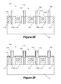
- FIG. 2E depicts the device 100 after an etching process has been performed to remove the gate cap layers 117 and portions of the sidewall spacers 116 .
- the etching process is performed for a sufficient duration such that the upper surface 116 X of the spacers 116 is below the upper surface 115 S of the sacrificial gate electrode 115 . This etching process results in the definition of reduced-height sidewall spacers 116 A.
- FIG. 2F-2G depict the device 100 after sidewall spacers 130 S have been formed on the exposed upstanding portions of the layer of insulating material 120 that were previously covered by the removed portions of the sidewall spacers 116 .
- the spacers 130 S contact the underlying reduced-height sidewall spacer 116 A.
- the process begins by depositing a layer of spacer material 130 (see FIG. 2F ) and thereafter performing an anisotropic etching process to define the spacer 130 S.
- the sidewall spacer 130 S may be comprised of a variety of different materials, e.g., silicon nitride, silicon carbon nitride, silicon carbon boron nitride, etc.
- the material selected for the spacer 130 S should be a material that will withstand the etching processes that are performed to remove the sacrificial gate structures and the pre-clean process, typically using dilute HF acid, that is performed prior to forming replacement gate structures on the device 100 .
- the base thickness of the sidewall spacer 130 may vary depending upon the particular application. In one illustrative embodiment, the sidewall spacer 130 may have a thickness at its base of about 5-10 nm. The width of the spacers 130 S at their base may or may not be sufficient to cover the entire width 120 X (see FIG.
- the reduced-height sidewall spacers 116 A e.g., the base width of the spacer 130 S may be less than the width 120 X.
- FIG. 2H depicts the device 100 after one or more etching processes have been performed to remove the sacrificial gate electrodes 115 and the sacrificial gate insulation layers 114 to thereby define a plurality of gate cavities 122 where replacement gate structures will subsequently be formed.
- a first, upper portion 122 A of the gate cavity 122 has a width that is laterally defined by the spacers 130 S while a lower portion 122 L of the gate cavity 122 has a width that is laterally defined by the thickness of the original spacers 116 .
- the sacrificial gate insulation layer 114 is removed as part of the replacement gate technique, as depicted herein.
- the sacrificial gate insulation layer 114 may not be removed in all applications. Even in cases where the sacrificial gate insulation layer 114 is intentionally removed, there will typically be a very thin native oxide layer (not shown) that forms on the substrate 112 within the gate cavities 122 .
- FIG. 2I depicts the device 100 after schematically depicted replacement gate structures 124 have been formed in the gate cavities 122 .
- the device will typically be subjected to a pre-clean process to insure that all non-desired materials are removed from the surface of the substrate 112 prior to forming the layers of material that will be part of the replacement gate structure 124 .
- this pre-clean process is performed with HF acid. Note that, using the novel process flow disclosed herein, the spacers 130 S protect the upstanding portions of the layer of insulating material 120 during this pre-clean process. Accordingly, the insulating material 120 is less likely to be significantly degraded during the HF pre-clean process.
- the problems identified in the background section of the application may be avoided or reduced.
- traditional manufacturing operations may be performed to complete the formation of the device 100 .
- the replacement gate structures 124 could be further recessed and re-filled with dielectric cap material.
- various metallization layers may be subsequently formed above the device 100 using known processing techniques.
- FIGS. 3A-3D depict another illustrative process flow disclosed herein form forming replacement gate structures on integrated circuit devices.
- FIG. 3A corresponds to the point of fabrication shown in FIG. 2G , i.e., after the formation of the spacers 130 S.
- FIG. 3B with the spacers 130 S in position, an etching process is performed to form a recess 116 R in the reduced-height spacers 116 A.
- the depth and width of the recesses 116 R may vary depending upon the particular application, e.g., the vertical depth of the recesses 116 R may be about 10-30 nm, while the lateral width of the recesses 116 R may be about 5-10 nm. Note that in the depicted embodiment, the recesses 116 R are self-aligned with respect to the sidewall spacers 130 S.
- FIG. 3C depicts the device 100 after one or more etching processes have been performed to remove the sacrificial gate electrodes 115 and the sacrificial gate insulation layers 114 to thereby define a plurality of gate cavities 122 X where replacement gate structures will subsequently be formed.
- the width or size of the gate cavities 122 X is effectively increased (relative to the gate cavities 122 described above), thereby making the filling of the gate cavities 122 X with the multiple layers of material that will make up the replacement gate structure easier and less likely to create undesirable voids.
- the first, upper portion 122 A of the gate cavity 122 X has a width that is laterally defined by the spacers 130 S
- a second, intermediate portion 122 B of the gate cavity 122 X has a width that is laterally defined by the inner, substantially vertically oriented surfaces 116 V of the recesses 116 R formed in the reduced-height spacers 116 A and a third, lower portion 122 C of the gate cavity.
- the width of the gate cavities 122 , 122 X between the spacers 130 S may be about the same.
- the width of the gate cavities 122 , 122 X between the full thickness reduced-height spacers 116 A i.e., in the region right above the surface of the substrate 112 , may be about the same.
- FIG. 3D depicts the device 100 after schematically depicted replacement gate structures 124 A have been formed in the gate cavities 122 X.
- the device will typically be subjected to the previously mentioned HF acid pre-clean process to insure that all non-desired materials are removed from the surface of the substrate 112 prior to forming the layers of material that will be part of the replacement gate structure 124 A.
- the spacers 130 S protect the upstanding portions of the layer of insulating material 120 during this pre-clean process.
- traditional manufacturing operations may be performed to complete the formation of the device 100 .
- the replacement gate structures 124 A could be further recessed and re-filled with dielectric cap material.
- various metallization layers may be subsequently formed above the device 100 using known processing techniques.
- the replacement gate structures 124 , 124 A may vary depending upon the particular application.
- the replacement gate structures 124 , 124 A are each comprised of a high-k gate insulation layer, such as hafnium oxide, and one or more layers of metal.
- the layers of material that comprise the replacement gate structures 124 , 124 A are sequentially deposited in the gate cavities 122 , 122 X and one or more CMP processes are performed to remove excess portions of these layers of material to thereby arrive at the replacement gate structures 124 , 124 A depicted herein.
- FIGS. 4A and 4B are cross-sectional drawings of individual replacement gate structures 124 , 124 A made using the illustrative methods disclosed above in FIGS. 2A-2I and 3 A- 3 D, respectively.
- the internal spacers 130 S are formed between the replacement gate structures and the layer of insulating material 120 .
- the gate cavity 122 X has a more tapered configuration that should facilitate filling the gate cavity 122 X with the materials used for the replacement gate structure 124 A.
- the vertical location where there is a significant inward narrowing of the gate cavity 122 X due to the presence of the full width of the reduced-height spacer 116 A is moved closer to the substrate 112 , i.e., compare the location of the top surface 116 T of the reduced-height spacer 116 A (in the region indicated by dashed line 141 A) and the location of the bottom surface 116 B of the recesses 116 R (in the region indicated by dashed line 141 B).
- the gate cavity 122 X and resulting replacement gate structure 124 A is more tapered as compared to corresponding region 140 A of the gate cavity 122 and the replacement gate structure 124 formed when using the method shown in FIGS. 2A-2I .
- the spacer 130 S is positioned between the upper portion of the gate structures 124 , 124 A and the layer of insulating material 120 .
- the gate structures 124 , 124 A will have a configuration that substantially mirrors that of the corresponding gate cavities 122 , 122 X, respectively.
- a portion of a “replacement gate structure” is positioned relative to or between other structures, such as the spacers 130 S, it should be understood that such language is intended to include situations where any portion of any layer of insulating material or any layer of conductive material in the replacement gate structure is positioned relative to or between the other structures, i.e., it is not required that all of the various layers of material that comprise the replacement gate structure be positioned as indicated herein and/or in the claims.
- the device disclosed herein includes first and second spaced-apart portions of a first layer of insulating material 120 positioned above a substrate 112 , a gate structure 124 , 124 A positioned above the substrate between the first and second spaced-apart portions of the first layer of insulating material 120 , a plurality of first sidewall spacers 130 S, each of which are positioned between the gate structure 124 , 124 A and on one of the first and second spaced-apart portions of the first layer of insulating material 120 and a second sidewall spacer 116 A positioned below each of the first sidewall spacers 130 S, wherein the first sidewall spacer 130 S contacts the second sidewall spacer 116 A.
- the replacement gate structures 124 , 124 A depicted in the drawings are intended to be representative in nature.
- the gate insulation layer in such replacement gate structures may be comprised of a variety of different materials, such as, for example, silicon dioxide, a so-called high-k (k greater than 10) insulation material (where k is the relative dielectric constant), etc.
- the gate electrode in such replacement gate structures may be comprised of one or more layers of conductive material, e.g., polysilicon, tungsten, aluminum, one or more layers of metal, etc.
- a metal layer such as a very thin work function adjusting metal (e.g., a layer of titanium nitride), may be formed on the high-k gate insulation layer.
- the insulating materials and the metal layer(s) that are part of the replacement gate structures 124 , 124 A may be of any desired construction and comprised of any of a variety of different materials.
- the replacement gate structures 124 , 124 A for an NFET device may have different material combinations as compared to the replacement gate structures 124 , 124 A for a PFET device.
- the particular details of construction of the replacement gate structures 124 , 124 A and the manner in which such replacement gate structures 124 , 124 A are formed should not be considered a limitation of the present invention unless such limitations are expressly recited in the attached claims.
Abstract
Description
Claims (15)
Priority Applications (1)
| Application Number | Priority Date | Filing Date | Title |
|---|---|---|---|
| US13/671,940 US8772101B2 (en) | 2012-11-08 | 2012-11-08 | Methods of forming replacement gate structures on semiconductor devices and the resulting device |
Applications Claiming Priority (1)
| Application Number | Priority Date | Filing Date | Title |
|---|---|---|---|
| US13/671,940 US8772101B2 (en) | 2012-11-08 | 2012-11-08 | Methods of forming replacement gate structures on semiconductor devices and the resulting device |
Publications (2)
| Publication Number | Publication Date |
|---|---|
| US20140124841A1 US20140124841A1 (en) | 2014-05-08 |
| US8772101B2 true US8772101B2 (en) | 2014-07-08 |
Family
ID=50621556
Family Applications (1)
| Application Number | Title | Priority Date | Filing Date |
|---|---|---|---|
| US13/671,940 Active US8772101B2 (en) | 2012-11-08 | 2012-11-08 | Methods of forming replacement gate structures on semiconductor devices and the resulting device |
Country Status (1)
| Country | Link |
|---|---|
| US (1) | US8772101B2 (en) |
Cited By (2)
| Publication number | Priority date | Publication date | Assignee | Title |
|---|---|---|---|---|
| US20150118836A1 (en) * | 2013-10-28 | 2015-04-30 | United Microelectronics Corp. | Method of fabricating semiconductor device |
| US11123321B2 (en) | 2002-10-23 | 2021-09-21 | Vifor (International) Ag | Aqueous iron carbohydrate complexes, their production and medicaments containing them |
Families Citing this family (18)
| Publication number | Priority date | Publication date | Assignee | Title |
|---|---|---|---|---|
| US9824881B2 (en) | 2013-03-14 | 2017-11-21 | Asm Ip Holding B.V. | Si precursors for deposition of SiN at low temperatures |
| US20140273531A1 (en) * | 2013-03-14 | 2014-09-18 | Asm Ip Holding B.V. | Si PRECURSORS FOR DEPOSITION OF SiN AT LOW TEMPERATURES |
| US9564309B2 (en) | 2013-03-14 | 2017-02-07 | Asm Ip Holding B.V. | Si precursors for deposition of SiN at low temperatures |
| US8912057B1 (en) * | 2013-06-05 | 2014-12-16 | Globalfoundries Inc. | Fabrication of nickel free silicide for semiconductor contact metallization |
| US9576790B2 (en) | 2013-10-16 | 2017-02-21 | Asm Ip Holding B.V. | Deposition of boron and carbon containing materials |
| US9543140B2 (en) | 2013-10-16 | 2017-01-10 | Asm Ip Holding B.V. | Deposition of boron and carbon containing materials |
| US9153483B2 (en) * | 2013-10-30 | 2015-10-06 | Taiwan Semiconductor Manufacturing Company, Ltd. | Method of semiconductor integrated circuit fabrication |
| US9401273B2 (en) | 2013-12-11 | 2016-07-26 | Asm Ip Holding B.V. | Atomic layer deposition of silicon carbon nitride based materials |
| US9576792B2 (en) | 2014-09-17 | 2017-02-21 | Asm Ip Holding B.V. | Deposition of SiN |
| US10410857B2 (en) | 2015-08-24 | 2019-09-10 | Asm Ip Holding B.V. | Formation of SiN thin films |
| US9722038B2 (en) | 2015-09-11 | 2017-08-01 | International Business Machines Corporation | Metal cap protection layer for gate and contact metallization |
| US10622457B2 (en) * | 2015-10-09 | 2020-04-14 | International Business Machines Corporation | Forming replacement low-K spacer in tight pitch fin field effect transistors |
| DE102016116026B4 (en) | 2015-12-29 | 2024-02-01 | Taiwan Semiconductor Manufacturing Co., Ltd. | Semiconductor device and manufacturing method |
| US10163704B2 (en) | 2015-12-29 | 2018-12-25 | Taiwan Semiconductor Manufacturing Co., Ltd. | Semiconductor device and a method for fabricating the same |
| US11056353B2 (en) | 2017-06-01 | 2021-07-06 | Asm Ip Holding B.V. | Method and structure for wet etch utilizing etch protection layer comprising boron and carbon |
| US10580645B2 (en) | 2018-04-30 | 2020-03-03 | Asm Ip Holding B.V. | Plasma enhanced atomic layer deposition (PEALD) of SiN using silicon-hydrohalide precursors |
| US11476347B2 (en) | 2020-05-20 | 2022-10-18 | Taiwan Semiconductor Manufacturing Co., Ltd. | Processes for removing spikes from gates |
| DE102020124588A1 (en) | 2020-05-20 | 2021-11-25 | Taiwan Semiconductor Manufacturing Co., Ltd. | PROCESSES TO REMOVE TIPS FROM GATES |
Citations (14)
| Publication number | Priority date | Publication date | Assignee | Title |
|---|---|---|---|---|
| US5973356A (en) * | 1997-07-08 | 1999-10-26 | Micron Technology, Inc. | Ultra high density flash memory |
| US20020066941A1 (en) * | 1998-05-28 | 2002-06-06 | Hidemitsu Aoki | Semiconductor device and method of manufacturing the same capable of reducing deterioration of low dielectric constant film |
| US6465823B1 (en) * | 1999-06-30 | 2002-10-15 | Kabushiki Kaisha Toshiba | Dynamic threshold voltage metal insulator semiconductor effect transistor |
| US6664592B2 (en) * | 1997-06-30 | 2003-12-16 | Kabushiki Kaisha Toshiba | Semiconductor device with groove type channel structure |
| US20050272191A1 (en) * | 2004-06-03 | 2005-12-08 | Uday Shah | Replacement gate process for making a semiconductor device that includes a metal gate electrode |
| US20060255469A1 (en) * | 1997-03-27 | 2006-11-16 | Renesas Technology Corp. | Semiconductor device and method of fabricating the same |
| US20070090417A1 (en) * | 2005-10-26 | 2007-04-26 | Chiaki Kudo | Semiconductor device and method for fabricating the same |
| US20080157146A1 (en) * | 2006-12-28 | 2008-07-03 | Jung-Kyu Kim | Image sensor and method for fabricating the same |
| US20080315318A1 (en) * | 2007-06-19 | 2008-12-25 | Yoshihiro Sato | Semiconductor device and manufacturing method thereof |
| US20090104789A1 (en) * | 2007-10-22 | 2009-04-23 | Applied Materials, Inc. | Method and system for improving dielectric film quality for void free gap fill |
| US7812411B2 (en) * | 2007-06-27 | 2010-10-12 | International Business Machines Corporation | High-k/metal gate MOSFET with reduced parasitic capacitance |
| US20110253965A1 (en) * | 2010-04-19 | 2011-10-20 | Micron Technology, Inc. | Vertical transistor phase change memory |
| US20120043623A1 (en) * | 2010-08-19 | 2012-02-23 | International Business Machines Corporation | Method and structure for forming high-k/metal gate extremely thin semiconductor on insulator device |
| US20120264286A1 (en) * | 2011-04-18 | 2012-10-18 | Samsung Electronics Co., Ltd. | Methods of manufacturing semiconductor devices |
-
2012
- 2012-11-08 US US13/671,940 patent/US8772101B2/en active Active
Patent Citations (14)
| Publication number | Priority date | Publication date | Assignee | Title |
|---|---|---|---|---|
| US20060255469A1 (en) * | 1997-03-27 | 2006-11-16 | Renesas Technology Corp. | Semiconductor device and method of fabricating the same |
| US6664592B2 (en) * | 1997-06-30 | 2003-12-16 | Kabushiki Kaisha Toshiba | Semiconductor device with groove type channel structure |
| US5973356A (en) * | 1997-07-08 | 1999-10-26 | Micron Technology, Inc. | Ultra high density flash memory |
| US20020066941A1 (en) * | 1998-05-28 | 2002-06-06 | Hidemitsu Aoki | Semiconductor device and method of manufacturing the same capable of reducing deterioration of low dielectric constant film |
| US6465823B1 (en) * | 1999-06-30 | 2002-10-15 | Kabushiki Kaisha Toshiba | Dynamic threshold voltage metal insulator semiconductor effect transistor |
| US20050272191A1 (en) * | 2004-06-03 | 2005-12-08 | Uday Shah | Replacement gate process for making a semiconductor device that includes a metal gate electrode |
| US20070090417A1 (en) * | 2005-10-26 | 2007-04-26 | Chiaki Kudo | Semiconductor device and method for fabricating the same |
| US20080157146A1 (en) * | 2006-12-28 | 2008-07-03 | Jung-Kyu Kim | Image sensor and method for fabricating the same |
| US20080315318A1 (en) * | 2007-06-19 | 2008-12-25 | Yoshihiro Sato | Semiconductor device and manufacturing method thereof |
| US7812411B2 (en) * | 2007-06-27 | 2010-10-12 | International Business Machines Corporation | High-k/metal gate MOSFET with reduced parasitic capacitance |
| US20090104789A1 (en) * | 2007-10-22 | 2009-04-23 | Applied Materials, Inc. | Method and system for improving dielectric film quality for void free gap fill |
| US20110253965A1 (en) * | 2010-04-19 | 2011-10-20 | Micron Technology, Inc. | Vertical transistor phase change memory |
| US20120043623A1 (en) * | 2010-08-19 | 2012-02-23 | International Business Machines Corporation | Method and structure for forming high-k/metal gate extremely thin semiconductor on insulator device |
| US20120264286A1 (en) * | 2011-04-18 | 2012-10-18 | Samsung Electronics Co., Ltd. | Methods of manufacturing semiconductor devices |
Non-Patent Citations (2)
| Title |
|---|
| Lee et al., Low Temperature Silicon Nitride and Silicon Dioxide Film Processing by Inductively Coupled Plasma Chemical Vapor Deposition, 2000, Journal of the Electrochemical Society, vol. 147, No. 4, 1481-1486. * |
| Lis et al., Application of flowable oxides in photonics, 2008, Materials Science-Poland, vol. 26, No. 1, 189-194. * |
Cited By (4)
| Publication number | Priority date | Publication date | Assignee | Title |
|---|---|---|---|---|
| US11123321B2 (en) | 2002-10-23 | 2021-09-21 | Vifor (International) Ag | Aqueous iron carbohydrate complexes, their production and medicaments containing them |
| US11291645B2 (en) | 2002-10-23 | 2022-04-05 | Vifor (International) Ag | Aqueous iron carbohydrate complexes, their production and medicaments containing them |
| US11590097B2 (en) | 2002-10-23 | 2023-02-28 | Vifor (International) Ag | Aqueous iron carbohydrate complexes, their production and medicaments containing them |
| US20150118836A1 (en) * | 2013-10-28 | 2015-04-30 | United Microelectronics Corp. | Method of fabricating semiconductor device |
Also Published As
| Publication number | Publication date |
|---|---|
| US20140124841A1 (en) | 2014-05-08 |
Similar Documents
| Publication | Publication Date | Title |
|---|---|---|
| US8772101B2 (en) | Methods of forming replacement gate structures on semiconductor devices and the resulting device | |
| US9953978B2 (en) | Replacement gate structures for transistor devices | |
| US9425280B2 (en) | Semiconductor device with low-K spacers | |
| US9236479B2 (en) | Methods of forming replacement gate structures and fins on FinFET devices and the resulting devices | |
| US9412822B2 (en) | Methods of forming stressed channel regions for a FinFET semiconductor device and the resulting device | |
| US9012319B1 (en) | Methods of forming gate structures with multiple work functions and the resulting products | |
| US9536877B2 (en) | Methods of forming different spacer structures on integrated circuit products having differing gate pitch dimensions and the resulting products | |
| US8809178B2 (en) | Methods of forming bulk FinFET devices with replacement gates so as to reduce punch through leakage currents | |
| US9064890B1 (en) | Methods of forming isolation material on FinFET semiconductor devices and the resulting devices | |
| US20160190306A1 (en) | Finfet device with a substantially self-aligned isolation region positioned under the channel region | |
| US9263580B2 (en) | Methods of forming isolated channel regions for a FinFET semiconductor device and the resulting device | |
| US20150243604A1 (en) | Cap layers for semiconductor devices with self-aligned contact elements | |
| US9024388B2 (en) | Methods of forming gate structures for CMOS based integrated circuit products and the resulting devices | |
| US20150228776A1 (en) | Methods of forming contacts to semiconductor devices using a bottom etch stop layer and the resulting devices | |
| US9349840B2 (en) | Methods of forming stressed channel regions for a FinFET semiconductor device and the resulting device | |
| US9236258B2 (en) | Methods of forming gate structures for semiconductor devices using a replacement gate technique and the resulting devices | |
| US20150348970A1 (en) | Gate structures for cmos based integrated circuit products | |
| US8803254B2 (en) | Methods of forming replacement gate structures for NFET semiconductor devices and devices having such gate structures | |
| US9412740B2 (en) | Integrated circuit product with a gate height registration structure | |
| US20160013291A1 (en) | Methods of forming isolated channel regions for a finfet semiconductor device and the resulting device |
Legal Events
| Date | Code | Title | Description |
|---|---|---|---|
| AS | Assignment |
Owner name: GLOBALFOUNDRIES INC., CAYMAN ISLANDS Free format text: ASSIGNMENT OF ASSIGNORS INTEREST;ASSIGNORS:XIE, RUILONG;JIN, CHO;REEL/FRAME:029264/0481 Effective date: 20121029 Owner name: INTERNATIONAL BUSINESS MACHINES CORPORATION, NEW Y Free format text: ASSIGNMENT OF ASSIGNORS INTEREST;ASSIGNORS:SHOM, PONOTH;SURISETTY, CHARAN V.V.S.;SIGNING DATES FROM 20121026 TO 20121105;REEL/FRAME:029264/0506 |
|
| STCF | Information on status: patent grant |
Free format text: PATENTED CASE |
|
| AS | Assignment |
Owner name: GLOBALFOUNDRIES U.S. 2 LLC, NEW YORK Free format text: ASSIGNMENT OF ASSIGNORS INTEREST;ASSIGNOR:INTERNATIONAL BUSINESS MACHINES CORPORATION;REEL/FRAME:036550/0001 Effective date: 20150629 |
|
| AS | Assignment |
Owner name: GLOBALFOUNDRIES INC., CAYMAN ISLANDS Free format text: ASSIGNMENT OF ASSIGNORS INTEREST;ASSIGNORS:GLOBALFOUNDRIES U.S. 2 LLC;GLOBALFOUNDRIES U.S. INC.;REEL/FRAME:036779/0001 Effective date: 20150910 |
|
| MAFP | Maintenance fee payment |
Free format text: PAYMENT OF MAINTENANCE FEE, 4TH YEAR, LARGE ENTITY (ORIGINAL EVENT CODE: M1551) Year of fee payment: 4 |
|
| AS | Assignment |
Owner name: WILMINGTON TRUST, NATIONAL ASSOCIATION, DELAWARE Free format text: SECURITY AGREEMENT;ASSIGNOR:GLOBALFOUNDRIES INC.;REEL/FRAME:049490/0001 Effective date: 20181127 |
|
| AS | Assignment |
Owner name: GLOBALFOUNDRIES U.S. INC., CALIFORNIA Free format text: ASSIGNMENT OF ASSIGNORS INTEREST;ASSIGNOR:GLOBALFOUNDRIES INC.;REEL/FRAME:054633/0001 Effective date: 20201022 |
|
| AS | Assignment |
Owner name: GLOBALFOUNDRIES INC., CAYMAN ISLANDS Free format text: RELEASE BY SECURED PARTY;ASSIGNOR:WILMINGTON TRUST, NATIONAL ASSOCIATION;REEL/FRAME:054636/0001 Effective date: 20201117 |
|
| AS | Assignment |
Owner name: GLOBALFOUNDRIES U.S. INC., NEW YORK Free format text: RELEASE BY SECURED PARTY;ASSIGNOR:WILMINGTON TRUST, NATIONAL ASSOCIATION;REEL/FRAME:056987/0001 Effective date: 20201117 |
|
| MAFP | Maintenance fee payment |
Free format text: PAYMENT OF MAINTENANCE FEE, 8TH YEAR, LARGE ENTITY (ORIGINAL EVENT CODE: M1552); ENTITY STATUS OF PATENT OWNER: LARGE ENTITY Year of fee payment: 8 |