US8772175B2 - Method for manufacturing semiconductor device and semiconductor device - Google Patents
Method for manufacturing semiconductor device and semiconductor device Download PDFInfo
- Publication number
- US8772175B2 US8772175B2 US13/693,524 US201213693524A US8772175B2 US 8772175 B2 US8772175 B2 US 8772175B2 US 201213693524 A US201213693524 A US 201213693524A US 8772175 B2 US8772175 B2 US 8772175B2
- Authority
- US
- United States
- Prior art keywords
- silicon layer
- shaped silicon
- fin
- pillar
- upper portion
- Prior art date
- Legal status (The legal status is an assumption and is not a legal conclusion. Google has not performed a legal analysis and makes no representation as to the accuracy of the status listed.)
- Active, expires
Links
- 238000004519 manufacturing process Methods 0.000 title claims abstract description 89
- 238000000034 method Methods 0.000 title claims description 79
- 239000004065 semiconductor Substances 0.000 title claims description 72
- 239000010410 layer Substances 0.000 claims abstract description 439
- XUIMIQQOPSSXEZ-UHFFFAOYSA-N Silicon Chemical compound [Si] XUIMIQQOPSSXEZ-UHFFFAOYSA-N 0.000 claims abstract description 324
- 229910052710 silicon Inorganic materials 0.000 claims abstract description 324
- 239000010703 silicon Substances 0.000 claims abstract description 324
- 229910021420 polycrystalline silicon Inorganic materials 0.000 claims abstract description 142
- 229920005591 polysilicon Polymers 0.000 claims abstract description 142
- 238000009792 diffusion process Methods 0.000 claims abstract description 114
- 229910052751 metal Inorganic materials 0.000 claims abstract description 81
- 239000002184 metal Substances 0.000 claims abstract description 81
- FVBUAEGBCNSCDD-UHFFFAOYSA-N silicide(4-) Chemical compound [Si-4] FVBUAEGBCNSCDD-UHFFFAOYSA-N 0.000 claims abstract description 28
- 229910021332 silicide Inorganic materials 0.000 claims abstract description 26
- 239000000758 substrate Substances 0.000 claims abstract description 26
- 238000000151 deposition Methods 0.000 claims abstract description 17
- 238000005530 etching Methods 0.000 claims abstract description 15
- 239000011229 interlayer Substances 0.000 claims abstract description 15
- 150000004767 nitrides Chemical class 0.000 claims description 47
- 239000012535 impurity Substances 0.000 claims description 17
- 238000005498 polishing Methods 0.000 claims description 12
- 239000000126 substance Substances 0.000 claims description 12
- 238000010438 heat treatment Methods 0.000 claims description 6
- 230000003071 parasitic effect Effects 0.000 description 7
- 230000003247 decreasing effect Effects 0.000 description 5
- 238000002513 implantation Methods 0.000 description 5
- 230000015572 biosynthetic process Effects 0.000 description 3
- 230000008021 deposition Effects 0.000 description 3
- 230000010354 integration Effects 0.000 description 3
- PXHVJJICTQNCMI-UHFFFAOYSA-N Nickel Chemical compound [Ni] PXHVJJICTQNCMI-UHFFFAOYSA-N 0.000 description 2
- ZOXJGFHDIHLPTG-UHFFFAOYSA-N Boron Chemical compound [B] ZOXJGFHDIHLPTG-UHFFFAOYSA-N 0.000 description 1
- OAICVXFJPJFONN-UHFFFAOYSA-N Phosphorus Chemical compound [P] OAICVXFJPJFONN-UHFFFAOYSA-N 0.000 description 1
- 229910052785 arsenic Inorganic materials 0.000 description 1
- RQNWIZPPADIBDY-UHFFFAOYSA-N arsenic atom Chemical compound [As] RQNWIZPPADIBDY-UHFFFAOYSA-N 0.000 description 1
- 238000000231 atomic layer deposition Methods 0.000 description 1
- 229910052796 boron Inorganic materials 0.000 description 1
- 229910017052 cobalt Inorganic materials 0.000 description 1
- 239000010941 cobalt Substances 0.000 description 1
- GUTLYIVDDKVIGB-UHFFFAOYSA-N cobalt atom Chemical compound [Co] GUTLYIVDDKVIGB-UHFFFAOYSA-N 0.000 description 1
- 238000011109 contamination Methods 0.000 description 1
- 238000004518 low pressure chemical vapour deposition Methods 0.000 description 1
- 238000012986 modification Methods 0.000 description 1
- 230000004048 modification Effects 0.000 description 1
- 229910052759 nickel Inorganic materials 0.000 description 1
- 238000000059 patterning Methods 0.000 description 1
- 229910052698 phosphorus Inorganic materials 0.000 description 1
- 239000011574 phosphorus Substances 0.000 description 1
- 238000001039 wet etching Methods 0.000 description 1
Images


Classifications
-
- H—ELECTRICITY
- H01—ELECTRIC ELEMENTS
- H01L—SEMICONDUCTOR DEVICES NOT COVERED BY CLASS H10
- H01L29/00—Semiconductor devices adapted for rectifying, amplifying, oscillating or switching, or capacitors or resistors with at least one potential-jump barrier or surface barrier, e.g. PN junction depletion layer or carrier concentration layer; Details of semiconductor bodies or of electrodes thereof ; Multistep manufacturing processes therefor
- H01L29/40—Electrodes ; Multistep manufacturing processes therefor
- H01L29/41—Electrodes ; Multistep manufacturing processes therefor characterised by their shape, relative sizes or dispositions
- H01L29/423—Electrodes ; Multistep manufacturing processes therefor characterised by their shape, relative sizes or dispositions not carrying the current to be rectified, amplified or switched
- H01L29/42312—Gate electrodes for field effect devices
- H01L29/42316—Gate electrodes for field effect devices for field-effect transistors
- H01L29/4232—Gate electrodes for field effect devices for field-effect transistors with insulated gate
- H01L29/42384—Gate electrodes for field effect devices for field-effect transistors with insulated gate for thin film field effect transistors, e.g. characterised by the thickness or the shape of the insulator or the dimensions, the shape or the lay-out of the conductor
- H01L29/42392—Gate electrodes for field effect devices for field-effect transistors with insulated gate for thin film field effect transistors, e.g. characterised by the thickness or the shape of the insulator or the dimensions, the shape or the lay-out of the conductor fully surrounding the channel, e.g. gate-all-around
-
- H—ELECTRICITY
- H01—ELECTRIC ELEMENTS
- H01L—SEMICONDUCTOR DEVICES NOT COVERED BY CLASS H10
- H01L29/00—Semiconductor devices adapted for rectifying, amplifying, oscillating or switching, or capacitors or resistors with at least one potential-jump barrier or surface barrier, e.g. PN junction depletion layer or carrier concentration layer; Details of semiconductor bodies or of electrodes thereof ; Multistep manufacturing processes therefor
- H01L29/66—Types of semiconductor device ; Multistep manufacturing processes therefor
- H01L29/66007—Multistep manufacturing processes
- H01L29/66075—Multistep manufacturing processes of devices having semiconductor bodies comprising group 14 or group 13/15 materials
- H01L29/66227—Multistep manufacturing processes of devices having semiconductor bodies comprising group 14 or group 13/15 materials the devices being controllable only by the electric current supplied or the electric potential applied, to an electrode which does not carry the current to be rectified, amplified or switched, e.g. three-terminal devices
- H01L29/66409—Unipolar field-effect transistors
- H01L29/66477—Unipolar field-effect transistors with an insulated gate, i.e. MISFET
- H01L29/66666—Vertical transistors
-
- H—ELECTRICITY
- H01—ELECTRIC ELEMENTS
- H01L—SEMICONDUCTOR DEVICES NOT COVERED BY CLASS H10
- H01L21/00—Processes or apparatus adapted for the manufacture or treatment of semiconductor or solid state devices or of parts thereof
- H01L21/70—Manufacture or treatment of devices consisting of a plurality of solid state components formed in or on a common substrate or of parts thereof; Manufacture of integrated circuit devices or of parts thereof
- H01L21/77—Manufacture or treatment of devices consisting of a plurality of solid state components or integrated circuits formed in, or on, a common substrate
- H01L21/78—Manufacture or treatment of devices consisting of a plurality of solid state components or integrated circuits formed in, or on, a common substrate with subsequent division of the substrate into plural individual devices
- H01L21/82—Manufacture or treatment of devices consisting of a plurality of solid state components or integrated circuits formed in, or on, a common substrate with subsequent division of the substrate into plural individual devices to produce devices, e.g. integrated circuits, each consisting of a plurality of components
- H01L21/822—Manufacture or treatment of devices consisting of a plurality of solid state components or integrated circuits formed in, or on, a common substrate with subsequent division of the substrate into plural individual devices to produce devices, e.g. integrated circuits, each consisting of a plurality of components the substrate being a semiconductor, using silicon technology
- H01L21/8232—Field-effect technology
- H01L21/8234—MIS technology, i.e. integration processes of field effect transistors of the conductor-insulator-semiconductor type
- H01L21/823487—MIS technology, i.e. integration processes of field effect transistors of the conductor-insulator-semiconductor type with a particular manufacturing method of vertical transistor structures, i.e. with channel vertical to the substrate surface
-
- H—ELECTRICITY
- H01—ELECTRIC ELEMENTS
- H01L—SEMICONDUCTOR DEVICES NOT COVERED BY CLASS H10
- H01L21/00—Processes or apparatus adapted for the manufacture or treatment of semiconductor or solid state devices or of parts thereof
- H01L21/70—Manufacture or treatment of devices consisting of a plurality of solid state components formed in or on a common substrate or of parts thereof; Manufacture of integrated circuit devices or of parts thereof
- H01L21/77—Manufacture or treatment of devices consisting of a plurality of solid state components or integrated circuits formed in, or on, a common substrate
- H01L21/78—Manufacture or treatment of devices consisting of a plurality of solid state components or integrated circuits formed in, or on, a common substrate with subsequent division of the substrate into plural individual devices
- H01L21/82—Manufacture or treatment of devices consisting of a plurality of solid state components or integrated circuits formed in, or on, a common substrate with subsequent division of the substrate into plural individual devices to produce devices, e.g. integrated circuits, each consisting of a plurality of components
- H01L21/822—Manufacture or treatment of devices consisting of a plurality of solid state components or integrated circuits formed in, or on, a common substrate with subsequent division of the substrate into plural individual devices to produce devices, e.g. integrated circuits, each consisting of a plurality of components the substrate being a semiconductor, using silicon technology
- H01L21/8232—Field-effect technology
- H01L21/8234—MIS technology, i.e. integration processes of field effect transistors of the conductor-insulator-semiconductor type
- H01L21/8238—Complementary field-effect transistors, e.g. CMOS
- H01L21/823807—Complementary field-effect transistors, e.g. CMOS with a particular manufacturing method of the channel structures, e.g. channel implants, halo or pocket implants, or channel materials
-
- H—ELECTRICITY
- H01—ELECTRIC ELEMENTS
- H01L—SEMICONDUCTOR DEVICES NOT COVERED BY CLASS H10
- H01L21/00—Processes or apparatus adapted for the manufacture or treatment of semiconductor or solid state devices or of parts thereof
- H01L21/70—Manufacture or treatment of devices consisting of a plurality of solid state components formed in or on a common substrate or of parts thereof; Manufacture of integrated circuit devices or of parts thereof
- H01L21/77—Manufacture or treatment of devices consisting of a plurality of solid state components or integrated circuits formed in, or on, a common substrate
- H01L21/78—Manufacture or treatment of devices consisting of a plurality of solid state components or integrated circuits formed in, or on, a common substrate with subsequent division of the substrate into plural individual devices
- H01L21/82—Manufacture or treatment of devices consisting of a plurality of solid state components or integrated circuits formed in, or on, a common substrate with subsequent division of the substrate into plural individual devices to produce devices, e.g. integrated circuits, each consisting of a plurality of components
- H01L21/822—Manufacture or treatment of devices consisting of a plurality of solid state components or integrated circuits formed in, or on, a common substrate with subsequent division of the substrate into plural individual devices to produce devices, e.g. integrated circuits, each consisting of a plurality of components the substrate being a semiconductor, using silicon technology
- H01L21/8232—Field-effect technology
- H01L21/8234—MIS technology, i.e. integration processes of field effect transistors of the conductor-insulator-semiconductor type
- H01L21/8238—Complementary field-effect transistors, e.g. CMOS
- H01L21/823885—Complementary field-effect transistors, e.g. CMOS with a particular manufacturing method of vertical transistor structures, i.e. with channel vertical to the substrate surface
-
- H—ELECTRICITY
- H01—ELECTRIC ELEMENTS
- H01L—SEMICONDUCTOR DEVICES NOT COVERED BY CLASS H10
- H01L27/00—Devices consisting of a plurality of semiconductor or other solid-state components formed in or on a common substrate
- H01L27/02—Devices consisting of a plurality of semiconductor or other solid-state components formed in or on a common substrate including semiconductor components specially adapted for rectifying, oscillating, amplifying or switching and having at least one potential-jump barrier or surface barrier; including integrated passive circuit elements with at least one potential-jump barrier or surface barrier
- H01L27/04—Devices consisting of a plurality of semiconductor or other solid-state components formed in or on a common substrate including semiconductor components specially adapted for rectifying, oscillating, amplifying or switching and having at least one potential-jump barrier or surface barrier; including integrated passive circuit elements with at least one potential-jump barrier or surface barrier the substrate being a semiconductor body
- H01L27/08—Devices consisting of a plurality of semiconductor or other solid-state components formed in or on a common substrate including semiconductor components specially adapted for rectifying, oscillating, amplifying or switching and having at least one potential-jump barrier or surface barrier; including integrated passive circuit elements with at least one potential-jump barrier or surface barrier the substrate being a semiconductor body including only semiconductor components of a single kind
- H01L27/085—Devices consisting of a plurality of semiconductor or other solid-state components formed in or on a common substrate including semiconductor components specially adapted for rectifying, oscillating, amplifying or switching and having at least one potential-jump barrier or surface barrier; including integrated passive circuit elements with at least one potential-jump barrier or surface barrier the substrate being a semiconductor body including only semiconductor components of a single kind including field-effect components only
- H01L27/088—Devices consisting of a plurality of semiconductor or other solid-state components formed in or on a common substrate including semiconductor components specially adapted for rectifying, oscillating, amplifying or switching and having at least one potential-jump barrier or surface barrier; including integrated passive circuit elements with at least one potential-jump barrier or surface barrier the substrate being a semiconductor body including only semiconductor components of a single kind including field-effect components only the components being field-effect transistors with insulated gate
- H01L27/092—Devices consisting of a plurality of semiconductor or other solid-state components formed in or on a common substrate including semiconductor components specially adapted for rectifying, oscillating, amplifying or switching and having at least one potential-jump barrier or surface barrier; including integrated passive circuit elements with at least one potential-jump barrier or surface barrier the substrate being a semiconductor body including only semiconductor components of a single kind including field-effect components only the components being field-effect transistors with insulated gate complementary MIS field-effect transistors
- H01L27/0924—Devices consisting of a plurality of semiconductor or other solid-state components formed in or on a common substrate including semiconductor components specially adapted for rectifying, oscillating, amplifying or switching and having at least one potential-jump barrier or surface barrier; including integrated passive circuit elements with at least one potential-jump barrier or surface barrier the substrate being a semiconductor body including only semiconductor components of a single kind including field-effect components only the components being field-effect transistors with insulated gate complementary MIS field-effect transistors including transistors with a horizontal current flow in a vertical sidewall of a semiconductor body, e.g. FinFET, MuGFET
-
- H—ELECTRICITY
- H01—ELECTRIC ELEMENTS
- H01L—SEMICONDUCTOR DEVICES NOT COVERED BY CLASS H10
- H01L29/00—Semiconductor devices adapted for rectifying, amplifying, oscillating or switching, or capacitors or resistors with at least one potential-jump barrier or surface barrier, e.g. PN junction depletion layer or carrier concentration layer; Details of semiconductor bodies or of electrodes thereof ; Multistep manufacturing processes therefor
- H01L29/02—Semiconductor bodies ; Multistep manufacturing processes therefor
- H01L29/06—Semiconductor bodies ; Multistep manufacturing processes therefor characterised by their shape; characterised by the shapes, relative sizes, or dispositions of the semiconductor regions ; characterised by the concentration or distribution of impurities within semiconductor regions
- H01L29/0603—Semiconductor bodies ; Multistep manufacturing processes therefor characterised by their shape; characterised by the shapes, relative sizes, or dispositions of the semiconductor regions ; characterised by the concentration or distribution of impurities within semiconductor regions characterised by particular constructional design considerations, e.g. for preventing surface leakage, for controlling electric field concentration or for internal isolations regions
- H01L29/0642—Isolation within the component, i.e. internal isolation
- H01L29/0649—Dielectric regions, e.g. SiO2 regions, air gaps
- H01L29/0653—Dielectric regions, e.g. SiO2 regions, air gaps adjoining the input or output region of a field-effect device, e.g. the source or drain region
-
- H—ELECTRICITY
- H01—ELECTRIC ELEMENTS
- H01L—SEMICONDUCTOR DEVICES NOT COVERED BY CLASS H10
- H01L29/00—Semiconductor devices adapted for rectifying, amplifying, oscillating or switching, or capacitors or resistors with at least one potential-jump barrier or surface barrier, e.g. PN junction depletion layer or carrier concentration layer; Details of semiconductor bodies or of electrodes thereof ; Multistep manufacturing processes therefor
- H01L29/66—Types of semiconductor device ; Multistep manufacturing processes therefor
- H01L29/68—Types of semiconductor device ; Multistep manufacturing processes therefor controllable by only the electric current supplied, or only the electric potential applied, to an electrode which does not carry the current to be rectified, amplified or switched
- H01L29/76—Unipolar devices, e.g. field effect transistors
- H01L29/772—Field effect transistors
- H01L29/78—Field effect transistors with field effect produced by an insulated gate
- H01L29/7827—Vertical transistors
-
- H—ELECTRICITY
- H01—ELECTRIC ELEMENTS
- H01L—SEMICONDUCTOR DEVICES NOT COVERED BY CLASS H10
- H01L29/00—Semiconductor devices adapted for rectifying, amplifying, oscillating or switching, or capacitors or resistors with at least one potential-jump barrier or surface barrier, e.g. PN junction depletion layer or carrier concentration layer; Details of semiconductor bodies or of electrodes thereof ; Multistep manufacturing processes therefor
- H01L29/66—Types of semiconductor device ; Multistep manufacturing processes therefor
- H01L29/68—Types of semiconductor device ; Multistep manufacturing processes therefor controllable by only the electric current supplied, or only the electric potential applied, to an electrode which does not carry the current to be rectified, amplified or switched
- H01L29/76—Unipolar devices, e.g. field effect transistors
- H01L29/772—Field effect transistors
- H01L29/78—Field effect transistors with field effect produced by an insulated gate
- H01L29/786—Thin film transistors, i.e. transistors with a channel being at least partly a thin film
- H01L29/78642—Vertical transistors
-
- H—ELECTRICITY
- H01—ELECTRIC ELEMENTS
- H01L—SEMICONDUCTOR DEVICES NOT COVERED BY CLASS H10
- H01L29/00—Semiconductor devices adapted for rectifying, amplifying, oscillating or switching, or capacitors or resistors with at least one potential-jump barrier or surface barrier, e.g. PN junction depletion layer or carrier concentration layer; Details of semiconductor bodies or of electrodes thereof ; Multistep manufacturing processes therefor
- H01L29/66—Types of semiconductor device ; Multistep manufacturing processes therefor
- H01L29/68—Types of semiconductor device ; Multistep manufacturing processes therefor controllable by only the electric current supplied, or only the electric potential applied, to an electrode which does not carry the current to be rectified, amplified or switched
- H01L29/76—Unipolar devices, e.g. field effect transistors
- H01L29/772—Field effect transistors
- H01L29/78—Field effect transistors with field effect produced by an insulated gate
- H01L29/786—Thin film transistors, i.e. transistors with a channel being at least partly a thin film
- H01L29/78651—Silicon transistors
- H01L29/78654—Monocrystalline silicon transistors
-
- H—ELECTRICITY
- H01—ELECTRIC ELEMENTS
- H01L—SEMICONDUCTOR DEVICES NOT COVERED BY CLASS H10
- H01L29/00—Semiconductor devices adapted for rectifying, amplifying, oscillating or switching, or capacitors or resistors with at least one potential-jump barrier or surface barrier, e.g. PN junction depletion layer or carrier concentration layer; Details of semiconductor bodies or of electrodes thereof ; Multistep manufacturing processes therefor
- H01L29/66—Types of semiconductor device ; Multistep manufacturing processes therefor
- H01L29/68—Types of semiconductor device ; Multistep manufacturing processes therefor controllable by only the electric current supplied, or only the electric potential applied, to an electrode which does not carry the current to be rectified, amplified or switched
- H01L29/76—Unipolar devices, e.g. field effect transistors
- H01L29/772—Field effect transistors
- H01L29/78—Field effect transistors with field effect produced by an insulated gate
- H01L29/786—Thin film transistors, i.e. transistors with a channel being at least partly a thin film
- H01L29/78696—Thin film transistors, i.e. transistors with a channel being at least partly a thin film characterised by the structure of the channel, e.g. multichannel, transverse or longitudinal shape, length or width, doping structure, or the overlap or alignment between the channel and the gate, the source or the drain, or the contacting structure of the channel
Definitions
- the present invention relates to a method for manufacturing a semiconductor device and to a semiconductor device.
- SGT surrounding gate transistors
- a metal for a gate electrode instead of using polysilicon, depletion can be suppressed, and the resistance of the gate electrode can be decreased.
- a manufacturing process after a metal gate is formed must be one in which metal contamination by the metal gate is always taken into consideration.
- a metal gate last process is used for actual products, in which a metal gate is formed after a high-temperature process (IEDM 2007 K. Mistry, et. al., pp. 247-250).
- the gate is formed using polysilicon, and then an interlayer insulating film is deposited. Then, the polysilicon gate is exposed by chemical mechanical polishing and etched, followed by deposition of a metal. Therefore, in order to satisfy both the metal gate process and the high-temperature process, the metal gate last process must be used for SGT, in which a metal gate is formed after the high-temperature process. Since, in the SGT, the top position of the pillar-shaped silicon layer is higher than the gate, some consideration is required for using the metal gate last process.
- MOS transistors use a first insulating film in order to decrease a parasitic capacitance between gate line and a substrate.
- a first insulating film is formed around a fin-shaped semiconductor layer and then etched back to expose the fin-shaped semiconductor layer, thereby decreasing the parasitic capacitance between the gate line and the substrate.
- the first insulating film must be used for decreasing the parasitic capacitance between the gate line and the substrate.
- the SGT includes the pillar-shaped semiconductor layer in addition to the fin-shaped semiconductor layer, and thus some consideration is required for forming the pillar-shaped semiconductor layer.
- FIN FET has been known, in which two transistors are formed from one dummy pattern (for example, Japanese Unexamined Patent Application Publication No. 2011-71235). A sidewall is formed around the dummy pattern and used as a mask for etching a substrate to form a fin, thereby forming two transistors from one dummy pattern.
- one of the transistors can be used as an nMOS transistor and the other one can be used a pMOS transistor.
- an object is to decrease a parasitic capacitance between a gate line and a substrate, provide a CMOS SGT manufacturing method for forming nMOS SGT and pMOS SGT from one dummy pattern using a gate last process, and provide a resulting SGT structure.
- a method for manufacturing a semiconductor device of the present invention includes: a first step of forming a first fin-shaped silicon layer and a second fin-shaped silicon layer on a substrate so that the first fin-shaped silicon layer and the second fin-shaped silicon layer are connected to each other at the ends thereof to form a closed loop, forming a first insulating film around the first fin-shaped silicon layer and the second fin-shaped silicon layer, forming a first pillar-shaped silicon layer on the first fin-shaped silicon layer, and forming a second pillar-shaped silicon layer on the second fin-shaped silicon layer, the width of the first pillar-shaped silicon layer being equal to the width of the first fin-shaped silicon layer and the width of the second pillar-shaped silicon layer being equal to the width of the second fin-shaped silicon layer; a second step of, after the first step, forming n-type diffusion layers by implanting impurities in an upper portion of the first pillar-shaped silicon layer, an upper portion of the first fin-shaped silicon layer, and a lower portion of the first pillar-
- the manufacturing method is also characterized in that in the first step, a second oxide film is deposited for forming a dummy pattern on the substrate, a first resist is formed for forming the dummy pattern, the second oxide film is etched to form the dummy pattern, the first resist is removed, a first nitride film is deposited and then etched to be left as a sidewall and to form a first nitride film sidewall around the dummy pattern, the dummy pattern is removed, the silicon substrate is etched using the first nitride film sidewall as a mask to form the first fin-shaped silicon layer and the second fin-shaped silicon layer which are connected to each other at the ends to form a closed loop, the first insulating film is formed around the first fin-shaped silicon layer and the second fin-shaped silicon layer, the first nitride film sidewall is removed, the first insulating film is etched back to expose upper portions of the first fin-shaped silicon layer and the second fin-shaped silicon layer, a second resist is formed to
- the manufacturing method is further characterized in that in the second step after the first step, in the whole structure after the first step, a third oxide film is deposited, a second nitride film is formed and then etched to be left as a sidewall, a third resist is formed for forming the n-type diffusion layers, impurities are implanted to form the n-type diffusion layers in an upper portion of the first pillar-shaped silicon layer and an upper portion of the first fin-shaped silicon layer, the third resist is removed, the second nitride film and the third oxide film are removed, heat treatment is performed, a fourth oxide film is deposited, a third nitride film is formed and then etched to be left as a sidewall, a fourth resist is formed for forming the p-type diffusion layers, impurities are implanted to form the p-type diffusion layers in an upper portion of the second pillar-shaped silicon layer and an upper portion of the second fin-shaped silicon layer, the fourth resist is removed, the fourth oxide film and the third nit
- the manufacturing method is further characterized in that in the third step after the second step, the gate insulating film is formed to surround the pillar-shaped silicon layers, polysilicon is deposited and then planarized so that after planarization, the top surface of the polysilicon is higher than the gate insulating film on the n-type diffusion layer formed in the upper portion of the first pillar-shaped silicon layer and higher than the gate insulating film on the p-type diffusion layer formed in the upper portion of the second pillar-shaped silicon layer, a fourth nitride film is deposited, a fifth resist is formed for forming the first polysilicon gate electrode, the second polysilicon gate electrode, and the polysilicon gate line, the fourth nitride film is etched, the polysilicon is etched to form the first polysilicon gate electrode, the second polysilicon gate electrode, and the polysilicon gate line, the gate insulating films are etched, and the fifth resist is removed.
- the manufacturing method is further characterized in that in the fourth step, in the whole structure after the third step, a fifth nitride film is deposited and then etched to be left as a sidewall, and a metal is deposited to form silicides in upper portions of the n-type diffusion layer and the p-type diffusion layer in the upper portions of the first fin-shaped silicon layer and the second fin-shaped silicon layer, respectively.
- the manufacturing method is further characterized in that in the fifth step, in the whole structure after the fourth step, a sixth nitride film is deposited, the interlayer insulating film is deposited and then planarized by chemical mechanical polishing, the first polysilicon gate electrode, the second polysilicon gate electrode, and the polysilicon gate line are exposed by chemical mechanical polishing, the first polysilicon gate electrode, the second polysilicon gate electrode, and the polysilicon gate line are etched, a metal is deposited to be filled in portions from which the first polysilicon gate electrode, the second polysilicon gate electrode, and the polysilicon gate line have been removed, and the metal is etched to expose the gate insulating film on the n-type diffusion layer in the upper portion of the first pillar-shaped silicon layer and expose the gate insulating film on the p-type diffusion layer in the upper portion of the second pillar-shaped silicon layer, thereby forming the first metal gate electrode, the second metal gate electrode, and the metal gate line.
- a semiconductor device of the present invention includes: a first fin-shaped silicon layer formed on a substrate; a second fin-shaped silicon layer formed on the substrate, the first fin-shaped silicon layer and the second fin-shaped silicon layer being connected to each other at the ends thereof to form a closed loop; a first insulating film formed around the first fin-shaped silicon layer and the second fin-shaped silicon layer; a first pillar-shaped silicon layer formed on the first fin-shaped silicon layer; a second pillar-shaped silicon layer formed on the second fin-shaped silicon layer, the width of the first pillar-shaped silicon layer being equal to the width of the first fin-shaped silicon layer and the width of the second pillar-shaped silicon layer being equal to the width of the second fin-shaped silicon layer; an n-type diffusion layer formed in an upper portion of the first fin-shaped silicon layer and a lower portion of the first pillar-shaped silicon layer; an n-type diffusion layer formed in an upper portion of the first pillar-shaped silicon layer; a p-type diffusion layer formed in an upper portion of the second fin
- CMOS SGT manufacturing method for forming nMOS SGT and pMOS SGT from one dummy pattern using a gate last process, and provide a resulting SGT structure.
- the manufacturing method is based on a conventional FINFET manufacturing method in which a sidewall is formed around a dummy pattern and used as a mask for etching a substrate to form a fin, thereby forming two transistors from one dummy pattern, and thus two SGTs can be easily formed from one dummy pattern.
- CMOS SGT can be formed from one dummy pattern, and thus CMOS SGT with high integration can be provided.
- a silicide is generally formed in an upper portion of a pillar-shaped silicon layer, but a silicide must be formed after a polysilicon gate is formed because the deposition temperature of polysilicon is higher than the silicide formation temperature. Therefore, when the silicide is formed in an upper portion of a silicon column, a hole is formed on a polysilicon gate electrode after the polysilicon gate is formed, the silicide is formed after a sidewall composed of an insulating film is formed on the sidewall of the hole, and then the hole is filled with an insulating film, thereby causing the problem of increasing the number of manufacturing steps.
- the diffusion layers are formed before the polysilicon gate electrode and the polysilicon gate line are formed, the pillar-shaped silicon layer is covered with the polysilicon gate electrode, and the silicide is formed only in an upper portion of the fin-shaped silicon layer. Therefore, a usual metal gate last manufacturing method can be used, in which a gate is formed using polysilicon, the interlayer insulating film is deposited, the polysilicon gate is exposed by chemical mechanical polishing and then etched, and then a metal is deposited, thereby facilitating the formation of metal gate CMOS SGT.
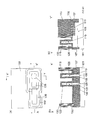
- FIG. 1( a ) is a plan view of a semiconductor device according to the present invention
- FIG. 1( b ) is a sectional view taken along line X-X′ in FIG. 1( a )
- FIG. 1( c ) is a sectional view taken along line Y-Y′ in FIG. 1( a ).
- FIG. 2( a ) is a plan view of a method for manufacturing a semiconductor device according to the present invention
- FIG. 2( b ) is a sectional view taken along line X-X′ in FIG. 2( a )
- FIG. 2( c ) is a sectional view taken along line Y-Y′ in FIG. 2( a ).
- FIG. 3( a ) is a plan view of a method for manufacturing a semiconductor device according to the present invention
- FIG. 3( b ) is a sectional view taken along line X-X′ in FIG. 3( a )
- FIG. 3( c ) is a sectional view taken along line Y-Y′ in FIG. 3( a ).
- FIG. 4( a ) is a plan view of a method for manufacturing a semiconductor device according to the present invention
- FIG. 4( b ) is a sectional view taken along line X-X′ in FIG. 4( a )
- FIG. 4( c ) is a sectional view taken along line Y-Y′ in FIG. 4( a ).
- FIG. 5( a ) is a plan view of a method for manufacturing a semiconductor device according to the present invention
- FIG. 5( b ) is a sectional view taken along line X-X′ in FIG. 5( a )
- FIG. 5( c ) is a sectional view taken along line Y-Y′ in FIG. 5( a ).
- FIG. 6( a ) is a plan view of a method for manufacturing a semiconductor device according to the present invention
- FIG. 6( b ) is a sectional view taken along line X-X′ in FIG. 6( a )
- FIG. 6( c ) is a sectional view taken along line Y-Y′ in FIG. 6( a ).
- FIG. 7( a ) is a plan view of a method for manufacturing a semiconductor device according to the present invention
- FIG. 7( b ) is a sectional view taken along line X-X′ in FIG. 7( a )
- FIG. 7( c ) is a sectional view taken along line Y-Y′ in FIG. 7( a ).
- FIG. 8( a ) is a plan view of a method for manufacturing a semiconductor device according to the present invention
- FIG. 8( b ) is a sectional view taken along line X-X′ in FIG. 8( a )
- FIG. 8( c ) is a sectional view taken along line Y-Y′ in FIG. 8( a ).
- FIG. 9( a ) is a plan view of a method for manufacturing a semiconductor device according to the present invention
- FIG. 9( b ) is a sectional view taken along line X-X′ in FIG. 9( a )
- FIG. 9( c ) is a sectional view taken along line Y-Y′ in FIG. 9( a ).
- FIG. 10( a ) is a plan view of a method for manufacturing a semiconductor device according to the present invention
- FIG. 10( b ) is a sectional view taken along line X-X′ in FIG. 10( a )
- FIG. 10( c ) is a sectional view taken along line Y-Y′ in FIG. 10( a ).
- FIG. 11( a ) is a plan view of a method for manufacturing a semiconductor device according to the present invention
- FIG. 11( b ) is a sectional view taken along line X-X′ in FIG. 11( a )
- FIG. 11( c ) is a sectional view taken along line Y-Y′ in FIG. 11( a ).
- FIG. 12( a ) is a plan view of a method for manufacturing a semiconductor device according to the present invention
- FIG. 12( b ) is a sectional view taken along line X-X′ in FIG. 12( a )
- FIG. 12( c ) is a sectional view taken along line Y-Y′ in FIG. 12( a ).
- FIG. 13( a ) is a plan view of a method for manufacturing a semiconductor device according to the present invention
- FIG. 13( b ) is a sectional view taken along line X-X′ in FIG. 13( a )
- FIG. 13( c ) is a sectional view taken along line Y-Y′ in FIG. 13( a ).
- FIG. 14( a ) is a plan view of a method for manufacturing a semiconductor device according to the present invention
- FIG. 14( b ) is a sectional view taken along line X-X′ in FIG. 14( a )
- FIG. 14( c ) is a sectional view taken along line Y-Y′ in FIG. 14( a ).
- FIG. 15( a ) is a plan view of a method for manufacturing a semiconductor device according to the present invention
- FIG. 15( b ) is a sectional view taken along line X-X′ in FIG. 15( a )
- FIG. 15( c ) is a sectional view taken along line Y-Y′ in FIG. 15( a ).
- FIG. 16( a ) is a plan view of a method for manufacturing a semiconductor device according to the present invention
- FIG. 16( b ) is a sectional view taken along line X-X′ in FIG. 16( a )
- FIG. 16( c ) is a sectional view taken along line Y-Y′ in FIG. 16( a ).
- FIG. 17( a ) is a plan view of a method for manufacturing a semiconductor device according to the present invention
- FIG. 17( b ) is a sectional view taken along line X-X′ in FIG. 17( a )
- FIG. 17( c ) is a sectional view taken along line Y-Y′ in FIG. 17( a ).
- FIG. 18( a ) is a plan view of a method for manufacturing a semiconductor device according to the present invention
- FIG. 18( b ) is a sectional view taken along line X-X′ in FIG. 18( a )
- FIG. 18( c ) is a sectional view taken along line Y-Y′ in FIG. 18( a ).
- FIG. 19( a ) is a plan view of a method for manufacturing a semiconductor device according to the present invention
- FIG. 19( b ) is a sectional view taken along line X-X′ in FIG. 19( a )
- FIG. 19( c ) is a sectional view taken along line Y-Y′ in FIG. 19( a ).
- FIG. 20( a ) is a plan view of a method for manufacturing a semiconductor device according to the present invention
- FIG. 20( b ) is a sectional view taken along line X-X′ in FIG. 20( a )
- FIG. 20( c ) is a sectional view taken along line Y-Y′ in FIG. 20( a ).
- FIG. 21( a ) is a plan view of a method for manufacturing a semiconductor device according to the present invention
- FIG. 21( b ) is a sectional view taken along line X-X′ in FIG. 21( a )
- FIG. 21( c ) is a sectional view taken along line Y-Y′ in FIG. 21( a ).
- FIG. 22( a ) is a plan view of a method for manufacturing a semiconductor device according to the present invention
- FIG. 22( b ) is a sectional view taken along line X-X′ in FIG. 22( a )
- FIG. 22( c ) is a sectional view taken along line Y-Y′ in FIG. 22( a ).
- FIG. 23( a ) is a plan view of a method for manufacturing a semiconductor device according to the present invention
- FIG. 23( b ) is a sectional view taken along line X-X′ in FIG. 23( a )
- FIG. 23( c ) is a sectional view taken along line Y-Y′ in FIG. 23( a ).
- FIG. 24( a ) is a plan view of a method for manufacturing a semiconductor device according to the present invention
- FIG. 24( b ) is a sectional view taken along line X-X′ in FIG. 24( a )
- FIG. 24( c ) is a sectional view taken along line Y-Y′ in FIG. 24( a ).
- FIG. 25( a ) is a plan view of a method for manufacturing a semiconductor device according to the present invention
- FIG. 25( b ) is a sectional view taken along line X-X′ in FIG. 25( a )
- FIG. 25( c ) is a sectional view taken along line Y-Y′ in FIG. 25( a ).
- FIG. 26( a ) is a plan view of a method for manufacturing a semiconductor device according to the present invention
- FIG. 26( b ) is a sectional view taken along line X-X′ in FIG. 26( a )
- FIG. 26( c ) is a sectional view taken along line Y-Y′ in FIG. 26( a ).
- FIG. 27( a ) is a plan view of a method for manufacturing a semiconductor device according to the present invention
- FIG. 27( b ) is a sectional view taken along line X-X′ in FIG. 27( a )
- FIG. 27( c ) is a sectional view taken along line Y-Y′ in FIG. 27( a ).
- FIG. 28( a ) is a plan view of a method for manufacturing a semiconductor device according to the present invention
- FIG. 28( b ) is a sectional view taken along line X-X′ in FIG. 28( a )
- FIG. 28( c ) is a sectional view taken along line Y-Y′ in FIG. 28( a ).
- FIG. 29( a ) is a plan view of a method for manufacturing a semiconductor device according to the present invention
- FIG. 29( b ) is a sectional view taken along line X-X′ in FIG. 29( a )
- FIG. 29( c ) is a sectional view taken along line Y-Y′ in FIG. 29( a ).
- FIG. 30( a ) is a plan view of a method for manufacturing a semiconductor device according to the present invention
- FIG. 30( b ) is a sectional view taken along line X-X′ in FIG. 30( a )
- FIG. 30( c ) is a sectional view taken along line Y-Y′ in FIG. 30( a ).
- FIG. 31( a ) is a plan view of a method for manufacturing a semiconductor device according to the present invention
- FIG. 31( b ) is a sectional view taken along line X-X′ in FIG. 31( a )
- FIG. 31( c ) is a sectional view taken along line Y-Y′ in FIG. 31( a ).
- FIG. 32( a ) is a plan view of a method for manufacturing a semiconductor device according to the present invention
- FIG. 32( b ) is a sectional view taken along line X-X′ in FIG. 32( a )
- FIG. 32( c ) is a sectional view taken along line Y-Y′ in FIG. 32( a ).
- FIG. 33( a ) is a plan view of a method for manufacturing a semiconductor device according to the present invention
- FIG. 33( b ) is a sectional view taken along line X-X′ in FIG. 33( a )
- FIG. 33( c ) is a sectional view taken along line Y-Y′ in FIG. 33( a ).
- FIG. 34( a ) is a plan view of a method for manufacturing a semiconductor device according to the present invention
- FIG. 34( b ) is a sectional view taken along line X-X′ in FIG. 34( a )
- FIG. 34( c ) is a sectional view taken along line Y-Y′ in FIG. 34( a ).
- FIG. 35( a ) is a plan view of a method for manufacturing a semiconductor device according to the present invention
- FIG. 35( b ) is a sectional view taken along line X-X′ in FIG. 35( a )
- FIG. 35( c ) is a sectional view taken along line Y-Y′ in FIG. 35( a ).
- FIG. 36( a ) is a plan view of a method for manufacturing a semiconductor device according to the present invention
- FIG. 36( b ) is a sectional view taken along line X-X′ in FIG. 36( a )
- FIG. 36( c ) is a sectional view taken along line Y-Y′ in FIG. 36( a ).
- FIG. 37( a ) is a plan view of a method for manufacturing a semiconductor device according to the present invention
- FIG. 37( b ) is a sectional view taken along line X-X′ in FIG. 37( a )
- FIG. 37( c ) is a sectional view taken along line Y-Y′ in FIG. 37( a ).
- FIG. 38( a ) is a plan view of a method for manufacturing a semiconductor device according to the present invention
- FIG. 38( b ) is a sectional view taken along line X-X′ in FIG. 38( a )
- FIG. 38( c ) is a sectional view taken along line Y-Y′ in FIG. 38( a ).
- FIG. 39( a ) is a plan view of a method for manufacturing a semiconductor device according to the present invention
- FIG. 39( b ) is a sectional view taken along line X-X′ in FIG. 39( a )
- FIG. 39( c ) is a sectional view taken along line Y-Y′ in FIG. 39( a ).
- FIG. 40( a ) is a plan view of a method for manufacturing a semiconductor device according to the present invention
- FIG. 40( b ) is a sectional view taken along line X-X′ in FIG. 40( a )
- FIG. 40( c ) is a sectional view taken along line Y-Y′ in FIG. 40( a ).
- FIG. 41( a ) is a plan view of a method for manufacturing a semiconductor device according to the present invention
- FIG. 41( b ) is a sectional view taken along line X-X′ in FIG. 41( a )
- FIG. 41( c ) is a sectional view taken along line Y-Y′ in FIG. 41( a ).
- FIG. 42( a ) is a plan view of a method for manufacturing a semiconductor device according to the present invention
- FIG. 42( b ) is a sectional view taken along line X-X′ in FIG. 42( a )
- FIG. 42( c ) is a sectional view taken along line Y-Y′ in FIG. 42( a ).
- FIG. 43( a ) is a plan view of a method for manufacturing a semiconductor device according to the present invention
- FIG. 43( b ) is a sectional view taken along line X-X′ in FIG. 43( a )
- FIG. 43( c ) is a sectional view taken along line Y-Y′ in FIG. 43( a ).
- FIG. 44( a ) is a plan view of a method for manufacturing a semiconductor device according to the present invention
- FIG. 44( b ) is a sectional view taken along line X-X′ in FIG. 44( a )
- FIG. 44( c ) is a sectional view taken along line Y-Y′ in FIG. 44( a ).
- FIG. 45( a ) is a plan view of a method for manufacturing a semiconductor device according to the present invention
- FIG. 45( b ) is a sectional view taken along line X-X′ in FIG. 45( a )
- FIG. 45( c ) is a sectional view taken along line Y-Y′ in FIG. 45( a ).
- FIG. 46( a ) is a plan view of a method for manufacturing a semiconductor device according to the present invention
- FIG. 46( b ) is a sectional view taken along line X-X′ in FIG. 46( a )
- FIG. 46( c ) is a sectional view taken along line Y-Y′ in FIG. 46( a ).
- FIG. 47( a ) is a plan view of a method for manufacturing a semiconductor device according to the present invention
- FIG. 47( b ) is a sectional view taken along line X-X′ in FIG. 47( a )
- FIG. 47( c ) is a sectional view taken along line Y-Y′ in FIG. 47( a ).
- FIG. 48( a ) is a plan view of a method for manufacturing a semiconductor device according to the present invention
- FIG. 48( b ) is a sectional view taken along line X-X′ in FIG. 48( a )
- FIG. 48( c ) is a sectional view taken along line Y-Y′ in FIG. 48( a ).
- FIG. 49( a ) is a plan view of a method for manufacturing a semiconductor device according to the present invention
- FIG. 49( b ) is a sectional view taken along line X-X′ in FIG. 49( a )
- FIG. 49( c ) is a sectional view taken along line Y-Y′ in FIG. 49( a ).
- FIG. 50( a ) is a plan view of a method for manufacturing a semiconductor device according to the present invention
- FIG. 50( b ) is a sectional view taken along line X-X′ in FIG. 50( a )
- FIG. 50( c ) is a sectional view taken along line Y-Y′ in FIG. 50( a ).
- FIG. 51( a ) is a plan view of a method for manufacturing a semiconductor device according to the present invention
- FIG. 51( b ) is a sectional view taken along line X-X′ in FIG. 51( a )
- FIG. 51( c ) is a sectional view taken along line Y-Y′ in FIG. 51( a ).
- FIG. 52( a ) is a plan view of a method for manufacturing a semiconductor device according to the present invention
- FIG. 52( b ) is a sectional view taken along line X-X′ in FIG. 52( a )
- FIG. 52( c ) is a sectional view taken along line Y-Y′ in FIG. 52( a ).
- a manufacturing process for forming a SGT structure according to an embodiment of the present invention is described below with reference to FIGS. 2 to 52 .
- a second oxide film 102 is formed for forming a dummy pattern on a silicon substrate 101 .
- a nitride film or a laminated film of an oxide film and polysilicon may be used.
- a first resist 103 is formed for forming the dummy pattern.
- the second oxide film 102 is etched to form the dummy pattern 102 .
- the first resist 103 is removed.
- a first nitride film 104 is deposited.
- the first nitride film 104 is etched to be left as a sidewall. Consequently, a first nitride film sidewall 104 is formed around the dummy pattern 102 .
- the first nitride film sidewall 104 is used for etching silicon to form a first fin-shaped silicon layer 106 and a second fin-shaped silicon layer 105 which are connected to each other at the ends thereof to form a closed loop.
- the dummy pattern 102 is removed.
- the silicon substrate 101 is etched using the first nitride film sidewall 104 as a mask to form the first fin-shaped silicon layer 106 and the second fin-shaped silicon layer 105 which are connected to each other at the ends thereof to form a closed loop.
- a first insulating film 107 is formed around the first fin-shaped silicon layer 106 and the second fin-shaped silicon layer 105 .
- an oxide film formed by high-density plasma, or an oxide film formed by low-pressure chemical vapor deposition may be used.
- the first nitride film sidewall 104 is removed.
- this step is not required.
- the first insulating film 107 is etched back to expose an upper portion of the first fin-shaped silicon layer 106 and an upper portion of the second fin-shaped silicon layer 105 .
- a second resist 108 is formed so as to be perpendicular to the first fin-shaped silicon layer 106 and the second fin-shaped silicon layer 105 .
- the first fin-shaped silicon layer 106 and the second fin-shaped silicon layer are etched.
- a portion where the first fin-shaped silicon layer 106 and the second resist 108 intersect at right angles becomes a first pillar-shaped silicon layer 110 .
- a portion where the second fin-shaped silicon layer 105 and the second resist 108 intersect at right angles becomes a second pillar-shaped silicon layer 109 . Therefore, the width of the first pillar-shaped silicon layer 110 is equal to the width of the first fin-shaped silicon layer 106 .
- the width of the second pillar-shaped silicon layer 109 is equal to the width of the second fin-shaped silicon layer 105 .
- the first pillar-shaped silicon layer 110 is formed in an upper portion of the first fin-shaped silicon layer 106
- the second pillar-shaped silicon layer 109 is formed in an upper portion of the second fin-shaped silicon layer 105
- the first insulating film 107 is formed around the first fin-shaped silicon layer 106 and the second fin-shaped silicon layer 105 .
- the second resist 108 is removed.
- n-type diffusion layers are formed by implanting impurities in an upper portion of the first pillar-shaped silicon layer 110 , an upper portion of the first fin-shaped silicon layer 106 , and a lower portion of the first pillar-shaped silicon layer 110
- p-type diffusion layers are formed by implanting impurities in an upper portion of the second pillar-shaped silicon layer 109 , an upper portion of the second fin-shaped silicon layer 105 , and a lower portion of the second pillar-shaped silicon layer 109 .
- a third oxide film 111 is deposited, and a second nitride film 112 is formed. Since upper portions of the pillar-shaped silicon layers are subsequently covered with a gate insulating film and polysilicon gate electrodes, diffusion layers are formed in upper portions of the pillar-shaped silicon layers before covering of the pillar-shaped silicon layers.
- the second nitride film 112 is etched to be left as a sidewall.
- a third resist 113 is formed for forming the n-type diffusion layers by impurity implantation in an upper portion of the first pillar-shaped silicon layer 110 , an upper portion of the first fin-shaped silicon layer 106 , and a lower portion of the first pillar-shaped silicon layer 110 .
- impurities such as arsenic or phosphorus are implanted to form a n-type diffusion layer 115 in an upper portion of the first pillar-shaped silicon layer 110 , and n-type diffusion layers 116 and 117 in an upper portion of the first fin-shaped silicon layer 106 .
- the third resist 113 is removed.
- the second nitride film 112 and the third oxide film 111 are removed.
- n-type diffusion layers 116 and 117 in an upper portion of the first fin-shaped silicon layer 106 are brought into contact with each other to form a n-type diffusion layer 118 .
- a fourth oxide film 119 is deposited, and a third nitride film 120 is formed. Since upper portions of the pillar-shaped silicon layers are subsequently covered with a gate insulating film and polysilicon gate electrodes, diffusion layers are formed in upper portions of the pillar-shaped silicon layers before the pillar-shaped silicon layers are covered.
- the third nitride film 120 is etched to be left as a sidewall.
- a fourth resist 121 is formed for forming the p-type diffusion layers by impurity implantation in an upper portion of the second pillar-shaped silicon layer 109 , an upper portion of the second fin-shaped silicon layer 105 , and a lower portion of the second pillar-shaped silicon layer 109 .
- impurities such as boron are implanted to form a p-type diffusion layer 122 in an upper portion of the second pillar-shaped silicon layer 109 , and p-type diffusion layers 123 and 124 in an upper portion of the second fin-shaped silicon layer 105 .
- the fourth resist 121 is removed.
- the third nitride film 120 and the fourth oxide film 119 are removed.
- heat treatment is performed.
- the p-type diffusion layers 123 and 124 in an upper portion of the second fin-shaped silicon layer 105 are brought into contact with each other to form a n-type diffusion layer 125 .
- the n-type diffusion layers 115 and 118 are formed by impurity implantation in an upper portion of the first pillar-shaped silicon layer 110 and in an upper portion of the first fin-shaped silicon layer 106 and a lower portion of the first pillar-shaped silicon layer 110
- the p-type diffusion layers 122 and 125 are formed by impurity implantation in an upper portion of the second pillar-shaped silicon layer 109 and in an upper portion of the second fin-shaped silicon layer 105 and a lower portion of the second pillar-shaped silicon layer 109 .
- CMOS SGT can be formed from one dummy pattern.
- the line width of the dummy pattern is minimum feature size F
- the distance between the first pillar-shaped silicon layer 110 and the second pillar-shaped silicon layer 109 is the minimum feature size F. Therefore, an allowance for alignment of a resist mask for impurity implantation can be made F/2, thereby making it easy to separate between pMOS and nMOS elements.
- an interlayer insulating film is deposited, and then the polysilicon gate electrodes and the polysilicon gate line are exposed by chemical mechanical polishing. Therefore, it is necessary to prevent upper portions of the pillar-shaped silicon layers from being exposed by chemical mechanical polishing.
- a gate insulating film 126 is formed, and polysilicon 127 is deposited and then planarized. After planarization, the top position of the polysilicon 127 is higher than the gate insulating film 126 disposed on the n-type diffusion layer 115 in an upper portion of the first pillar-shaped silicon layer 110 and higher than the gate insulating film 126 disposed on the p-type diffusion layer 122 in an upper portion of the second pillar-shaped silicon layer 109 .
- the polysilicon gate electrodes and the polysilicon gate line are exposed by chemical mechanical polishing after the interlayer insulating film is deposited, the upper portions of the pillar-shaped silicon layers are not exposed by chemical mechanical polishing.
- a fourth nitride film 128 is deposited.
- the fourth nitride film 128 is a film which inhibits the formation of silicide in upper portions of the first polysilicon gate electrode 127 a , the second polysilicon gate electrode 127 b , and the polysilicon gate line 127 c when the silicide is formed in upper portions of the first fin-shaped silicon layer 106 and the second fin-shaped silicon layer 105 .
- a fifth resist 129 is formed for forming the first polysilicon gate electrode 127 a , the second polysilicon gate electrode 127 b , and the polysilicon gate line 127 c .
- a portion corresponding to the gate line is preferably perpendicular to the first fin-shaped silicon layer 106 and the second fin-shaped silicon layer 105 . This is because a parasitic capacitance between the gate line and the substrate is decreased.
- the fourth nitride film 128 is etched, and the polysilicon 127 is etched to form the first polysilicon gate electrode 127 a , the second polysilicon gate electrode 127 b , and the polysilicon gate line 127 c.
- the gate insulating film 126 is etched.
- the fifth resist 129 is removed.
- the manufacturing method for forming, using polysilicon, the first polysilicon gate electrode 127 a , the second polysilicon gate electrode 127 b , and the polysilicon gate line 127 c in order to use the gate-last process is described above.
- the top position of polysilicon is higher than the gate insulating film 126 on the n-type diffusion layer 115 in an upper portion of the first pillar-shaped silicon layer 110 and higher than the gate insulating film 126 on the p-type diffusion layer 122 in an upper portion of the second pillar-shaped silicon layer 109 .
- a silicide is not formed in upper portions of the first polysilicon gate electrode 127 a , the second polysilicon gate electrode 127 b , and the polysilicon gate line 127 c , in the n-type diffusion layer 115 in an upper portion of the first pillar-shaped silicon layer 110 , and in the p-type diffusion layer 122 in an upper portion of the second pillar-shaped silicon layer 109 .
- the manufacturing process is enlarged.
- a fifth nitride film 130 is deposited.
- the fifth nitride film 130 is etched to be left as a sidewall.
- a metal such as nickel or cobalt is deposited to form silicide 131 in upper portions of the n-type diffusion layer 118 and the p-type diffusion layer 125 formed in upper portions of the first fin-shaped silicon layer 106 and the second fin-shaped silicon layer 105 , respectively.
- the first polysilicon gate electrode 127 a , the second polysilicon gate electrode 127 b , and the polysilicon gate line 127 c are covered with the fifth nitride film 130 and the fourth nitride film 128 , and the n-type diffusion layer 115 in an upper portion of the first pillar-shaped silicon layer 110 and the p-type diffusion layer 122 in an upper portion of the second pillar-shaped silicon layer 109 are covered with the gate insulating film 126 , the first polysilicon gate electrode 127 a , the second polysilicon gate electrode 127 b , and the polysilicon gate line 127 c , and thus a silicide is not formed in these portions.
- the manufacturing method for forming a silicide in an upper portion of the n-type diffusion layer 118 in an upper portion of the first fin-shaped silicon layer 106 and in an upper portion of the p-type diffusion layer 125 in an upper portion of the second fin-shaped silicon layer 105 is described above.
- a gate-last manufacturing method in which after an interlayer insulting film 133 is deposited, the first polysilicon gate electrode 127 a , the second polysilicon gate electrode 127 b , and the polysilicon gate line 127 c are exposed, the first polysilicon gate electrode 127 a , the second polysilicon gate electrode 127 b , and the polysilicon gate line 127 c are etched, and then a metal is deposited to form a first metal gate electrode 134 a , a second metal gate electrode 134 b , and a metal gate line 134 c.
- a sixth nitride film 132 is deposited for protecting the silicide 131 .
- an interlayer insulating film 133 is deposited and then planarized by chemical mechanical polishing.
- the first polysilicon gate electrode 127 a , the second polysilicon gate electrode 127 b , and the polysilicon gate line 127 c are exposed by chemical mechanical polishing.
- the first polysilicon gate electrode 127 a , the second polysilicon gate electrode 127 b , and the polysilicon gate line 127 c are etched. Wet etching is preferred.
- a metal 134 is deposited and then planarized to fill, with the metal 134 , portions from which the first polysilicon gate electrode 127 a , the second polysilicon gate electrode 127 b , and the polysilicon gate line 127 c have been removed.
- Atomic layer deposition is preferably used.
- the metal 134 is etched to expose the gate insulating film 126 formed on the n-type diffusion layer 115 in an upper portion of the first pillar-shaped silicon layer 110 and expose the gate insulating film 126 formed on the p-type diffusion layer 122 in an upper portion of the second pillar-shaped silicon layer 109 . Consequently, the first metal gate electrode 134 a , the second metal gate electrode 134 b , and the metal gate line 134 c are formed.
- the gate-last manufacturing method is described above, in which after the interlayer insulating film 133 is deposited, the first polysilicon gate electrode 127 a , the second polysilicon gate electrode 127 b , and the polysilicon gate line 127 c are exposed, the first polysilicon gate electrode 127 a , the second polysilicon gate electrode 127 b , and the polysilicon gate line 127 c are etched, and then the metal 134 is deposited to form the first metal gate electrode 134 a , the second metal gate electrode 134 b , and the metal gate line 134 c.
- a manufacturing method for forming a contact is described. Since a silicide is not formed in the n-type diffusion layer 115 in an upper portion of the first pillar-shaped silicon layer 110 and in the p-type diffusion layer 122 in an upper portion of the second pillar-shaped silicon layer 109 , a first contact is brought into direct contact with the n-type diffusion layer 115 in an upper portion of the first pillar-shaped silicon layer 110 and a second contact is brought into direct contact with the p-type diffusion layer 122 in an upper portion of the second pillar-shaped silicon layer 109 .
- an interlayer insulating film 135 is deposited and then planarized.
- a sixth resist 136 is formed for forming a first contact hole 138 on the first pillar-shaped silicon layer 110 and a second contact hole 137 on the second pillar-shaped silicon layer 109 . Then, the interlayer insulating film 135 is etched to form the first contact hole 138 and the second contact hole 137 .
- the sixth resist 136 is removed.
- a seventh resist 139 is formed for forming a third contact hole 140 and a fourth contact hole 141 on the metal gate line 134 c and on the first fin-shaped silicon layer 106 and the second fin-shaped silicon layer 105 .
- the interlayer insulating films 135 and 133 are etched to form the third contact hole 140 and the fourth contact hole 141 .
- the seventh resist 139 is removed, and the sixth nitride film 132 and the gate insulating film 126 are etched to expose the silicide 131 , the n-type diffusion layer 115 , and the p-type diffusion layer 122 . Then, a metal is deposited to form a first contact 144 , a second contact 143 , a third contact 142 , and a fourth contact 145 .
- the manufacturing method for forming contacts is described above. Since a silicide is not formed in the n-type diffusion layer 115 in an upper portion of the first pillar-shaped silicon layer 110 and in the p-type diffusion layer 122 in an upper portion of the second pillar-shaped silicon layer 109 , the first contact is brought into direct contact with the n-type diffusion layer 115 in an upper portion of the first pillar-shaped silicon layer 110 , and the second contact is brought into direct contact with the p-type diffusion layer 122 in an upper portion of the second pillar-shaped silicon layer 109 .
- a metal 146 is deposited.
- eighth resists 147 , 148 , 149 , and 150 are formed for forming the metal wiring, and the metal 146 is etched to form metal wirings 151 , 152 , 153 , and 154 .
- the eighth resists 147 , 148 , 149 , and 150 are removed.
- FIG. 1 The result of the above-described manufacturing method is shown in FIG. 1 .
- the resulting structure includes: the first fin-shaped silicon layer 106 formed on the substrate 101 and the second silicon layer 105 formed on the substrate 101 , the first fin-shaped silicon layer 106 and the second fin-shaped silicon layer 105 being connected to each other at the ends thereof to form a closed loop; the first insulating film 107 formed around the first fin-shaped silicon layer 106 and the second fin-shaped silicon layer 105 ; the first pillar-shaped silicon layer 110 formed on the first fin-shaped silicon layer 106 ; the second pillar-shaped silicon layer 109 formed on the second fin-shaped silicon layer 105 , the width of the first pillar-shaped silicon layer 110 being equal to the width of the first fin-shaped silicon layer 106 and the width of the second pillar-shaped silicon layer 109 being equal to the width of the second fin-shaped silicon layer 105 ; the n-type diffusion layer 118 formed in an upper portion of the first fin-shaped silicon layer 106 and a lower portion of the first pillar-shaped silicon layer 110 ; the n-type diffusion layer 115 formed
- CMOS SGT manufacturing method for forming a nMOS SGT and a pMOS SGT from one dummy pattern using a gate-last process and provide a resulting SGT structure.
Abstract
Description
Claims (7)
Priority Applications (8)
| Application Number | Priority Date | Filing Date | Title |
|---|---|---|---|
| US13/693,524 US8772175B2 (en) | 2011-12-19 | 2012-12-04 | Method for manufacturing semiconductor device and semiconductor device |
| US14/066,095 US8916478B2 (en) | 2011-12-19 | 2013-10-29 | Method for manufacturing semiconductor device and semiconductor device |
| US14/289,919 US9035384B2 (en) | 2011-12-19 | 2014-05-29 | Semiconductor device |
| US14/537,322 US9245889B2 (en) | 2011-12-19 | 2014-11-10 | Method for manufacturing semiconductor device and semiconductor device |
| US14/690,582 US9362353B2 (en) | 2011-12-19 | 2015-04-20 | Semiconductor device |
| US14/963,432 US9478545B2 (en) | 2011-12-19 | 2015-12-09 | Method for manufacturing semiconductor device and semiconductor device |
| US15/147,097 US9806163B2 (en) | 2011-12-19 | 2016-05-05 | Semiconductor device having an nMOS SGT and a pMOS SGT |
| US15/266,091 US9748244B2 (en) | 2011-12-19 | 2016-09-15 | Method for manufacturing semiconductor device and semiconductor device |
Applications Claiming Priority (2)
| Application Number | Priority Date | Filing Date | Title |
|---|---|---|---|
| US201161577189P | 2011-12-19 | 2011-12-19 | |
| US13/693,524 US8772175B2 (en) | 2011-12-19 | 2012-12-04 | Method for manufacturing semiconductor device and semiconductor device |
Related Child Applications (2)
| Application Number | Title | Priority Date | Filing Date |
|---|---|---|---|
| US14/066,095 Continuation-In-Part US8916478B2 (en) | 2011-12-19 | 2013-10-29 | Method for manufacturing semiconductor device and semiconductor device |
| US14/289,919 Continuation US9035384B2 (en) | 2011-12-19 | 2014-05-29 | Semiconductor device |
Publications (2)
| Publication Number | Publication Date |
|---|---|
| US20130153989A1 US20130153989A1 (en) | 2013-06-20 |
| US8772175B2 true US8772175B2 (en) | 2014-07-08 |
Family
ID=48609244
Family Applications (4)
| Application Number | Title | Priority Date | Filing Date |
|---|---|---|---|
| US13/693,524 Active 2032-12-20 US8772175B2 (en) | 2011-12-19 | 2012-12-04 | Method for manufacturing semiconductor device and semiconductor device |
| US14/289,919 Active US9035384B2 (en) | 2011-12-19 | 2014-05-29 | Semiconductor device |
| US14/690,582 Active US9362353B2 (en) | 2011-12-19 | 2015-04-20 | Semiconductor device |
| US15/147,097 Active US9806163B2 (en) | 2011-12-19 | 2016-05-05 | Semiconductor device having an nMOS SGT and a pMOS SGT |
Family Applications After (3)
| Application Number | Title | Priority Date | Filing Date |
|---|---|---|---|
| US14/289,919 Active US9035384B2 (en) | 2011-12-19 | 2014-05-29 | Semiconductor device |
| US14/690,582 Active US9362353B2 (en) | 2011-12-19 | 2015-04-20 | Semiconductor device |
| US15/147,097 Active US9806163B2 (en) | 2011-12-19 | 2016-05-05 | Semiconductor device having an nMOS SGT and a pMOS SGT |
Country Status (1)
| Country | Link |
|---|---|
| US (4) | US8772175B2 (en) |
Cited By (6)
| Publication number | Priority date | Publication date | Assignee | Title |
|---|---|---|---|---|
| US20140054681A1 (en) * | 2011-12-19 | 2014-02-27 | Unisantis Electronics Singapore Pte. Ltd. | Method for manufacturing semiconductor device and semiconductor device |
| US20140213025A1 (en) * | 2011-12-02 | 2014-07-31 | Unisantis Electronics Singapore Pte. Ltd. | Method for producing semiconductor device and semiconductor device |
| US20140264561A1 (en) * | 2011-12-19 | 2014-09-18 | Unisantis Electronics Singapore Pte. Ltd. | Semiconductor device |
| US9117690B2 (en) | 2011-12-02 | 2015-08-25 | Unisantis Electronics Singapore Pte. Ltd. | Method for producing semiconductor device and semiconductor device |
| US20160329326A1 (en) * | 2015-05-05 | 2016-11-10 | International Business Machines Corporation | Sub-fin doped bulk fin field effect transistor (finfet), integrated circuit (ic) and method of manufacture |
| US20180277538A1 (en) * | 2014-08-15 | 2018-09-27 | Taiwan Semiconductor Manufacturing Co., Ltd. | Method of fabricating integrated circuit |
Families Citing this family (13)
| Publication number | Priority date | Publication date | Assignee | Title |
|---|---|---|---|---|
| US8759178B2 (en) * | 2011-11-09 | 2014-06-24 | Unisantis Electronics Singapore Pte. Ltd. | Method for manufacturing semiconductor device and semiconductor device |
| US10438836B2 (en) | 2011-11-09 | 2019-10-08 | Unisantis Electronics Singapore Pte. Ltd. | Method for manufacturing a semiconductor device |
| US8697511B2 (en) | 2012-05-18 | 2014-04-15 | Unisantis Electronics Singapore Pte. Ltd. | Method for producing semiconductor device and semiconductor device |
| US8877578B2 (en) | 2012-05-18 | 2014-11-04 | Unisantis Electronics Singapore Pte. Ltd. | Method for producing semiconductor device and semiconductor device |
| JP5639317B1 (en) * | 2013-11-06 | 2014-12-10 | ユニサンティス エレクトロニクス シンガポール プライベート リミテッドUnisantis Electronics Singapore Pte Ltd. | Semiconductor device having SGT and manufacturing method thereof |
| WO2015075819A1 (en) | 2013-11-22 | 2015-05-28 | ユニサンティス エレクトロニクス シンガポール プライベート リミテッド | Semiconductor device, and manufacturing method for semiconductor device |
| US10276562B2 (en) | 2014-01-07 | 2019-04-30 | Taiwan Semiconductor Manufacturing Co., Ltd. | Semiconductor device with multiple threshold voltage and method of fabricating the same |
| WO2015125205A1 (en) * | 2014-02-18 | 2015-08-27 | ユニサンティス エレクトロニクス シンガポール プライベート リミテッド | Semiconductor device manufacturing method and semiconductor device |
| WO2015147843A1 (en) * | 2014-03-27 | 2015-10-01 | Intel Corporation | Precursor and process design for photo-assisted metal atomic layer deposition (ald) and chemical vapor deposition (cvd) |
| JP5798276B1 (en) * | 2014-06-16 | 2015-10-21 | ユニサンティス エレクトロニクス シンガポール プライベート リミテッドUnisantis Electronics Singapore Pte Ltd. | Semiconductor device manufacturing method and semiconductor device |
| US9373620B2 (en) | 2014-09-12 | 2016-06-21 | Taiwan Semiconductor Manufacturing Co., Ltd. | Series connected transistor structure and method of manufacturing the same |
| US10103247B1 (en) * | 2017-10-17 | 2018-10-16 | Globalfoundries Inc. | Vertical transistor having buried contact, and contacts using work function metals and silicides |
| US11081569B2 (en) * | 2017-12-15 | 2021-08-03 | International Business Machines Corporation | Resistor loaded inverter structures |
Citations (123)
| Publication number | Priority date | Publication date | Assignee | Title |
|---|---|---|---|---|
| US5017977A (en) | 1985-03-26 | 1991-05-21 | Texas Instruments Incorporated | Dual EPROM cells on trench walls with virtual ground buried bit lines |
| US5258635A (en) | 1988-09-06 | 1993-11-02 | Kabushiki Kaisha Toshiba | MOS-type semiconductor integrated circuit device |
| US5308782A (en) | 1992-03-02 | 1994-05-03 | Motorola | Semiconductor memory device and method of formation |
| US5312767A (en) | 1989-12-15 | 1994-05-17 | Mitsubishi Denki Kabushiki Kaisha | MOS type field effect transistor and manufacturing method thereof |
| WO1994014198A1 (en) | 1992-12-11 | 1994-06-23 | Intel Corporation | A mos transistor having a composite gate electrode and method of fabrication |
| US5382816A (en) | 1992-07-03 | 1995-01-17 | Mitsubishi Denki Kabushiki Kaisha | Semiconductor device having vertical transistor with tubular double-gate |
| US5416350A (en) | 1993-03-15 | 1995-05-16 | Kabushiki Kaisha Toshiba | Semiconductor device with vertical transistors connected in series between bit lines |
| US5627390A (en) | 1994-05-26 | 1997-05-06 | Mitsubishi Denki Kabushiki Kaisha | Semiconductor device with columns |
| US5656842A (en) | 1995-06-20 | 1997-08-12 | Mitsubishi Denki Kabushiki Kaisha | Vertical mosfet including a back gate electrode |
| US5703386A (en) | 1995-03-15 | 1997-12-30 | Sony Corporation | Solid-state image sensing device and its driving method |
| US5707885A (en) | 1995-05-26 | 1998-01-13 | Samsung Electronics Co., Ltd. | Method for manufacturing a vertical transistor having a storage node vertical transistor |
| US5710447A (en) | 1994-10-27 | 1998-01-20 | Nec Corporation | Solid state image device having a transparent Schottky electrode |
| US5767549A (en) | 1996-07-03 | 1998-06-16 | International Business Machines Corporation | SOI CMOS structure |
| US5811336A (en) | 1994-08-31 | 1998-09-22 | Nec Corporation | Method of forming MOS transistors having gate insulators of different thicknesses |
| US5994735A (en) | 1993-05-12 | 1999-11-30 | Mitsubishi Denki Kabushiki Kaisha | Semiconductor device having a vertical surround gate metal-oxide semiconductor field effect transistor, and manufacturing method thereof |
| JP2000012705A (en) | 1998-04-20 | 2000-01-14 | Nec Corp | Semiconductor storage device and its manufacture |
| JP2000244818A (en) | 1999-02-24 | 2000-09-08 | Sharp Corp | Amplifying solid-state image pickup device |
| US6121086A (en) | 1998-06-17 | 2000-09-19 | Hitachi, Ltd. | Method of manufacturing a semiconductor integrated circuit device and a semiconductor integrated circuit device |
| WO2001022494A1 (en) | 1999-09-21 | 2001-03-29 | Infineon Technologies Ag | Vertical pixel cells |
| JP2001237421A (en) | 2000-02-24 | 2001-08-31 | Toshiba Corp | Semiconductor device, sram and method of manufacturing the same |
| US6294418B1 (en) | 1998-02-24 | 2001-09-25 | Micron Technology, Inc. | Circuits and methods using vertical complementary transistors |
| JP2001339057A (en) | 2000-05-30 | 2001-12-07 | Mitsumasa Koyanagi | Method of manufacturing three-dimensional image processor |
| US20010052614A1 (en) | 2000-06-16 | 2001-12-20 | Shigeru Ishibashi | Semiconductor memory provided with vertical transistor and method of manufacturing the same |
| JP2001352047A (en) | 2000-06-05 | 2001-12-21 | Oki Micro Design Co Ltd | Semiconductor integrated circuit |
| US20020000624A1 (en) | 1999-02-22 | 2002-01-03 | Hitachi, Ltd. | Semiconductor device |
| JP2002033399A (en) | 2000-07-13 | 2002-01-31 | Toshiba Corp | Semiconductor integrated circuit and its manufacturing method |
| US20020034853A1 (en) | 1999-06-28 | 2002-03-21 | Mohsen Alavi | Structure and process flow for fabrication of dual gate floating body integrated mos transistors |
| US6373099B1 (en) | 1991-04-23 | 2002-04-16 | Canon Kabushiki Kaisha | Method of manufacturing a surrounding gate type MOFSET |
| US6406962B1 (en) | 2001-01-17 | 2002-06-18 | International Business Machines Corporation | Vertical trench-formed dual-gate FET device structure and method for creation |
| US20020110039A1 (en) | 2001-02-09 | 2002-08-15 | Micron Technology, Inc. | Memory address and decode circuits with ultra thin body transistors |
| JP2002231951A (en) | 2001-01-29 | 2002-08-16 | Sony Corp | Semiconductor device and its manufacturing method |
| JP2002246581A (en) | 2001-02-16 | 2002-08-30 | Sharp Corp | Image sensor and manufacturing method thereof |
| JP2002246580A (en) | 2001-02-16 | 2002-08-30 | Sharp Corp | Image sensor and manufacturing method thereof |
| US6461900B1 (en) | 2001-10-18 | 2002-10-08 | Chartered Semiconductor Manufacturing Ltd. | Method to form a self-aligned CMOS inverter using vertical device integration |
| US6483171B1 (en) | 1999-08-13 | 2002-11-19 | Micron Technology, Inc. | Vertical sub-micron CMOS transistors on (110), (111), (311), (511), and higher order surfaces of bulk, SOI and thin film structures and method of forming same |
| US20030002093A1 (en) | 2001-06-28 | 2003-01-02 | Jaroslav Hynecek | Active pixel image sensor with two transistor pixel, in-pixel non-uniformity correction, and bootstrapped reset lines |
| JP2003068883A (en) | 2001-08-24 | 2003-03-07 | Hitachi Ltd | Semiconductor storage device |
| JP2003224211A (en) | 2002-01-22 | 2003-08-08 | Hitachi Ltd | Semiconductor memory |
| US6624459B1 (en) | 2000-04-12 | 2003-09-23 | International Business Machines Corp. | Silicon on insulator field effect transistors having shared body contact |
| US6658259B2 (en) | 2002-03-07 | 2003-12-02 | Interwave Communications International, Ltd. | Wireless network having a virtual HLR and method of operating the same |
| US20040005755A1 (en) | 2002-07-08 | 2004-01-08 | Masahiro Moniwa | Semiconductor memory device and a method of manufacturing the same |
| US20040113207A1 (en) | 2002-12-11 | 2004-06-17 | International Business Machines Corporation | Vertical MOSFET SRAM cell |
| KR20040063348A (en) | 2003-01-07 | 2004-07-14 | 삼성전자주식회사 | Static random access memory having vertical transistors and method for fabricating the same |
| JP2004259733A (en) | 2003-02-24 | 2004-09-16 | Seiko Epson Corp | Solid-state image pickup device |
| US6815277B2 (en) | 2001-12-04 | 2004-11-09 | International Business Machines Corporation | Method for fabricating multiple-plane FinFET CMOS |
| JP2004319808A (en) | 2003-04-17 | 2004-11-11 | Takehide Shirato | Mis field effect transistor and its manufacturing method |
| US20040256639A1 (en) | 2003-06-17 | 2004-12-23 | International Business Machines Corporation | Low leakage heterojunction vertical transistors and high performance devices thereof |
| US20040262681A1 (en) | 2003-05-28 | 2004-12-30 | Fujio Masuoka | Semiconductor device |
| US6861684B2 (en) | 2001-04-02 | 2005-03-01 | Stmicroelectronics S.A. | Method of fabricating a vertical insulated gate transistor with low overlap of the gate on the source and the drain, and an integrated circuit including this kind of transistor |
| US6878991B1 (en) | 2004-01-30 | 2005-04-12 | Micron Technology, Inc. | Vertical device 4F2 EEPROM memory |
| CN1610126A (en) | 2003-10-16 | 2005-04-27 | 松下电器产业株式会社 | Solid-state imaging device and method of manufacturing the same |
| US6891225B2 (en) * | 2000-09-08 | 2005-05-10 | Kabushiki Kaisha Toshiba | Dynamic semiconductor memory device |
| US20050145911A1 (en) | 2001-02-09 | 2005-07-07 | Micron Technology, Inc. | Memory having a vertical transistor |
| US20050263821A1 (en) | 2004-05-25 | 2005-12-01 | Cho Young K | Multiple-gate MOS transistor and a method of manufacturing the same |
| US20050281119A1 (en) | 1997-08-21 | 2005-12-22 | Ryuji Shibata | Method of designing semiconductor integrated circuit device and semiconductor integrated circuit device |
| US20060007333A1 (en) | 2004-07-08 | 2006-01-12 | Sharp Kabushiki Kaisha | Solid-state image taking apparatus and method for fabricating the same |
| US20060006444A1 (en) | 2004-01-27 | 2006-01-12 | Micron Technology, Inc. | Selective epitaxy vertical integrated circuit components and methods |
| US20060046391A1 (en) | 2004-08-30 | 2006-03-02 | Tang Sanh D | Vertical wrap-around-gate field-effect-transistor for high density, low voltage logic and memory array |
| US20060043520A1 (en) | 2004-08-30 | 2006-03-02 | Dmitri Jerdev | Active photosensitive structure with buried depletion layer |
| US7052941B2 (en) | 2003-06-24 | 2006-05-30 | Sang-Yun Lee | Method for making a three-dimensional integrated circuit structure |
| JP2006294995A (en) | 2005-04-13 | 2006-10-26 | Nec Corp | Field-effect transistor and its manufacturing method |
| US20060261406A1 (en) | 2005-05-18 | 2006-11-23 | Yijian Chen | Vertical integrated-gate CMOS device and its fabrication process |
| US7198976B2 (en) | 2002-11-14 | 2007-04-03 | Sony Corporation | Solid-state imaging device and method for manufacturing the same |
| EP1770769A1 (en) | 2005-09-30 | 2007-04-04 | Commissariat à l'Energie Atomique | Vertical MOS transistor and method of producing the same |
| US20070075359A1 (en) | 2005-10-05 | 2007-04-05 | Samsung Electronics Co., Ltd. | Circuit device including vertical transistors connected to buried bitlines and method of manufacturing the same |
| US7233033B2 (en) | 1998-05-16 | 2007-06-19 | Semiconductor Energy Laboratory Co., Ltd. | Semiconductor device having pixels |
| CN1983601A (en) | 2005-09-02 | 2007-06-20 | 三星电子株式会社 | Dual-gate dynamic random access memory device and method of fabricating the same |
| US20070138557A1 (en) | 2003-07-15 | 2007-06-21 | Renesas Technology Corp. | Semiconductor device |
| US7271052B1 (en) | 2004-09-02 | 2007-09-18 | Micron Technology, Inc. | Long retention time single transistor vertical memory gain cell |
| US20080048245A1 (en) | 2006-08-23 | 2008-02-28 | Masaru Kito | Semiconductor device and manufacturing methods thereof |
| US7368334B2 (en) | 2003-04-04 | 2008-05-06 | Taiwan Semiconductor Manufacturing Company, Ltd. | Silicon-on-insulator chip with multiple crystal orientations |
| US20080173936A1 (en) | 2007-01-18 | 2008-07-24 | Samsung Electronics Co., Ltd. | Access device having vertical channel and related semiconductor device and a method of fabricating the access device |
| US7413480B2 (en) | 2004-08-19 | 2008-08-19 | Micron Technology, Inc. | Silicon pillars for vertical transistors |
| JP2008205168A (en) | 2007-02-20 | 2008-09-04 | Fujitsu Ltd | Semiconductor device and method of manufacturing the same |
| US20080210985A1 (en) | 2006-07-24 | 2008-09-04 | Kabushiki Kaisha Toshiba | Solid-state imaging device and manufacturing method thereof |
| US20080227241A1 (en) | 2007-03-12 | 2008-09-18 | Yukio Nakabayashi | Method of fabricating semiconductor device |
| JP2008300558A (en) | 2007-05-30 | 2008-12-11 | Unisantis Electronics Japan Ltd | Semiconductor device |
| US20090032955A1 (en) | 2007-08-03 | 2009-02-05 | Sony Corporation | Semiconductor device, its manufacturing method and display apparatus |
| US20090065832A1 (en) | 2007-09-12 | 2009-03-12 | Unisantis Electronics (Japan) Ltd. | Solid-state imaging device |
| US20090085088A1 (en) | 2007-09-28 | 2009-04-02 | Elpida Memory, Inc. | Semiconductor device and method of forming the same as well as data processing system including the semiconductor device |
| US20090114989A1 (en) | 2007-11-05 | 2009-05-07 | Kabushiki Kaisha Toshiba | Semiconductor memory device and manufacturing method thereof |
| WO2009057194A1 (en) | 2007-10-29 | 2009-05-07 | Unisantis Electronics (Japan) Ltd. | Semiconductor structure, and manufacturing method for that semiconductor structure |
| JP2009110049A (en) | 2007-10-26 | 2009-05-21 | Dainippon Printing Co Ltd | Authoring apparatus, method, and computer program |
| US20090159964A1 (en) | 2007-12-24 | 2009-06-25 | Hynix Semiconductor Inc. | Vertical channel transistor and method of fabricating the same |
| US20090174024A1 (en) | 2007-12-27 | 2009-07-09 | Tae-Gyu Kim | Image sensor and method for manufacturing the same |
| WO2009096470A1 (en) | 2008-01-29 | 2009-08-06 | Unisantis Electronics (Japan) Ltd. | Fabrication process of semiconductor device |
| WO2009096466A1 (en) | 2008-01-29 | 2009-08-06 | Unisantis Electronics (Japan) Ltd. | Semiconductor storage device |
| WO2009096001A1 (en) | 2008-01-29 | 2009-08-06 | Unisantis Electronics (Japan) Ltd. | Semiconductor storage device and memory embedded semiconductor device, and manufacturing method thereof |
| WO2009095997A1 (en) | 2008-01-29 | 2009-08-06 | Unisantis Electronics (Japan) Ltd. | Semiconductor device and its manufacturing method |
| WO2009096465A1 (en) | 2008-01-29 | 2009-08-06 | Unisantis Electronics (Japan) Ltd. | Semiconductor storage device |
| JP2009182316A (en) | 2008-01-29 | 2009-08-13 | Unisantis Electronics Japan Ltd | Semiconductor device |
| JP2009182317A (en) | 2008-01-29 | 2009-08-13 | Unisantis Electronics Japan Ltd | Fabrication process of semiconductor device |
| WO2009102059A1 (en) | 2008-02-15 | 2009-08-20 | Unisantis Electronics (Japan) Ltd. | Semiconductor device manufacturing method |
| US7579214B2 (en) | 2000-02-28 | 2009-08-25 | Semiconductor Energy Laboratory Co., Ltd. | Semiconductor device and a method of manufacturing the same |
| WO2009133957A1 (en) | 2008-05-02 | 2009-11-05 | 日本ユニサンティスエレクトロニクス株式会社 | Solid-state image pickup element |
| US20090291551A1 (en) | 2008-05-21 | 2009-11-26 | Hynix Semiconductor Inc. | Method for forming vertical channel transistor of semiconductor device |
| US20090290082A1 (en) | 1999-07-06 | 2009-11-26 | Semiconductor Energy Laboratory Co., Ltd. | Semiconductor Device and Fabrication Method Thereof |
| US20100052029A1 (en) | 2008-08-27 | 2010-03-04 | Wen-Kuei Huang | Transistor structure and dynamic random access memory structure including the same |
| US20100200731A1 (en) | 2007-09-12 | 2010-08-12 | Fujio Masuoka | Solid-state imaging device |
| US20100200913A1 (en) | 2008-01-29 | 2010-08-12 | Unisantis Electronics (Japan) Ltd. | Semiconductor storage device |
| US20100207201A1 (en) | 2008-01-29 | 2010-08-19 | Fujio Masuoka | Semiconductor device and production method therefor |
| US20100207200A1 (en) | 2007-12-05 | 2010-08-19 | Fujio Masuoka | Semiconductor device |
| US20100207172A1 (en) | 2007-10-29 | 2010-08-19 | Fujio Masuoka | Semiconductor structure and method of fabricating the semiconductor structure |
| US20100213539A1 (en) | 2008-01-29 | 2010-08-26 | Unisantis Electronics (Japan) Ltd. | Semiconductor device and production method therefor |
| US20100213525A1 (en) | 2008-01-29 | 2010-08-26 | Unisantis Electronics (Japan) Ltd. | Semiconductor storage device and methods of producing it |
| US20100219483A1 (en) | 2008-01-29 | 2010-09-02 | Fujio Masuoka | Semiconductor storage device |
| US20100219457A1 (en) | 2008-05-02 | 2010-09-02 | Fujio Masuoka | Solid-state imaging device |
| US20100270611A1 (en) | 2009-04-28 | 2010-10-28 | Fujio Masuoka | Semiconductor device including a mos transistor and production method therefor |
| US20100276750A1 (en) | 2009-05-01 | 2010-11-04 | Niko Semiconductor Co., Ltd. | Metal Oxide Semiconductor (MOS) Structure and Manufacturing Method Thereof |
| US20100295123A1 (en) | 2009-05-22 | 2010-11-25 | Macronix International Co., Ltd. | Phase Change Memory Cell Having Vertical Channel Access Transistor |
| US20110073925A1 (en) | 2009-09-30 | 2011-03-31 | Eun-Shil Park | Semiconductor device with buried bit lines interconnected to one-side-contact and fabrication method thereof |
| US7977736B2 (en) | 2006-02-23 | 2011-07-12 | Samsung Electronics Co., Ltd. | Vertical channel transistors and memory devices including vertical channel transistors |
| US7977738B2 (en) | 2008-07-28 | 2011-07-12 | Kabushiki Kaisha Toshiba | Semiconductor memory device and manufacturing method thereof |
| US20110215381A1 (en) | 2010-03-08 | 2011-09-08 | Fujio Masuoka | Solid state imaging device |
| JP2011211161A (en) | 2010-03-12 | 2011-10-20 | Unisantis Electronics Japan Ltd | Solid state imaging device |
| US20110254067A1 (en) | 2004-07-20 | 2011-10-20 | Micron Technology, Inc. | DRAM Layout with Vertical FETS and Method of Formation |
| US8067800B2 (en) | 2009-12-28 | 2011-11-29 | Force Mos Technology Co., Ltd. | Super-junction trench MOSFET with resurf step oxide and the method to make the same |
| US20110303973A1 (en) | 2010-06-15 | 2011-12-15 | Fujio Masuoka | Semiconductor device and production method |
| US20110303985A1 (en) | 2010-06-09 | 2011-12-15 | Fujio Masuoka | Semiconductor device and fabrication method therefor |
| US8110869B2 (en) | 2005-02-11 | 2012-02-07 | Alpha & Omega Semiconductor, Ltd | Planar SRFET using no additional masks and layout method |
| US20120086051A1 (en) | 2007-09-27 | 2012-04-12 | Fairchild Semiconductor Corporation | Semiconductor device with (110)-oriented silicon |
| US8227305B2 (en) | 2005-05-13 | 2012-07-24 | Micron Technology, Inc. | Memory array with ultra-thin etched pillar surround gate access transistors and buried data/bit lines |
| US8378400B2 (en) * | 2010-10-29 | 2013-02-19 | Unisantis Electronics Singapore Pte Ltd. | Solid state imaging device |
Family Cites Families (49)
| Publication number | Priority date | Publication date | Assignee | Title |
|---|---|---|---|---|
| JPS6070757A (en) | 1983-09-28 | 1985-04-22 | Hitachi Ltd | Semiconductor integrated circuit |
| JPS6113661U (en) | 1984-06-29 | 1986-01-27 | 菱有工業株式会社 | anti-fog mirror |
| JPS6113661A (en) | 1984-06-29 | 1986-01-21 | Nippon Telegr & Teleph Corp <Ntt> | Semiconductor device and manufacture thereof |
| JPS6245058A (en) | 1985-08-22 | 1987-02-27 | Nec Corp | Semiconductor device and its manufacture |
| JPH0799311B2 (en) | 1985-11-12 | 1995-10-25 | 石川島播磨重工業株式会社 | Heating furnace temperature control method |
| JPS62190751A (en) | 1986-02-17 | 1987-08-20 | Nec Corp | Semiconductor device |
| JPH0444683Y2 (en) | 1986-05-27 | 1992-10-21 | ||
| JPS6337633A (en) | 1986-07-31 | 1988-02-18 | Nec Corp | Semiconductor integrated circuit device |
| JPH0722182B2 (en) | 1986-12-23 | 1995-03-08 | 松下電子工業株式会社 | Complementary semiconductor device |
| JPS6489560A (en) | 1987-09-30 | 1989-04-04 | Sony Corp | Semiconductor memory |
| JPH01175775A (en) | 1987-12-29 | 1989-07-12 | Sharp Corp | Photo-driven mos semiconductor device |
| JPH0266969A (en) | 1988-08-31 | 1990-03-07 | Nec Corp | Semiconductor integrated circuit device |
| JP2703970B2 (en) | 1989-01-17 | 1998-01-26 | 株式会社東芝 | MOS type semiconductor device |
| JP3057661B2 (en) | 1988-09-06 | 2000-07-04 | 株式会社東芝 | Semiconductor device |
| JPH0289368A (en) | 1988-09-27 | 1990-03-29 | Sony Corp | Solid-state image sensing device |
| JPH0271556U (en) | 1988-11-18 | 1990-05-31 | ||
| JP2804539B2 (en) | 1989-09-28 | 1998-09-30 | 沖電気工業株式会社 | Semiconductor device and manufacturing method thereof |
| JP2950558B2 (en) | 1989-11-01 | 1999-09-20 | 株式会社東芝 | Semiconductor device |
| JPH03225873A (en) | 1990-01-30 | 1991-10-04 | Mitsubishi Electric Corp | Semiconductor device |
| JP2504601Y2 (en) | 1990-03-02 | 1996-07-10 | ポーラ化成工業株式会社 | Massage equipment |
| JPH04234166A (en) | 1990-12-28 | 1992-08-21 | Texas Instr Japan Ltd | Semiconductor integrated circuit device |
| JP3325072B2 (en) | 1992-03-02 | 2002-09-17 | モトローラ・インコーポレイテッド | Semiconductor memory device |
| JPH05276442A (en) | 1992-03-30 | 1993-10-22 | Hamamatsu Photonics Kk | Afterimage integration solid-state image pickup device |
| JPH06237003A (en) | 1993-02-10 | 1994-08-23 | Hitachi Ltd | Semiconductor memory device and manufacture thereof |
| JPH0669441U (en) | 1993-03-19 | 1994-09-30 | 川崎重工業株式会社 | Joint structure of dissimilar materials under corrosive environment |
| JP3957774B2 (en) | 1995-06-23 | 2007-08-15 | 株式会社東芝 | Semiconductor device |
| JPH1079482A (en) | 1996-08-09 | 1998-03-24 | Rai Hai | Ultrahigh-density integrated circuit |
| JP3036588B2 (en) | 1997-02-03 | 2000-04-24 | 日本電気株式会社 | Semiconductor storage device |
| JPH1187649A (en) | 1997-09-04 | 1999-03-30 | Hitachi Ltd | Semiconductor storage device |
| JP4078721B2 (en) | 1998-08-24 | 2008-04-23 | ソニー株式会社 | Semiconductor device and manufacturing method thereof |
| US6204187B1 (en) | 1999-01-06 | 2001-03-20 | Infineon Technologies North America, Corp. | Contact and deep trench patterning |
| JP2000357736A (en) | 1999-06-15 | 2000-12-26 | Toshiba Corp | Semiconductor device and manufacture thereof |
| DE60001601T2 (en) | 1999-06-18 | 2003-12-18 | Lucent Technologies Inc | Manufacturing process for manufacturing a CMOS integrated circuit with vertical transistors |
| JP2003142684A (en) | 2001-11-02 | 2003-05-16 | Toshiba Corp | Semiconductor element and semiconductor device |
| JP2004079694A (en) | 2002-08-14 | 2004-03-11 | Fujitsu Ltd | Standard cell |
| JP4639040B2 (en) | 2002-10-10 | 2011-02-23 | パナソニック株式会社 | Manufacturing method of semiconductor device |
| EP1609154B1 (en) | 2003-03-18 | 2013-12-25 | Kabushiki Kaisha Toshiba | Phase change memory device |
| US7612416B2 (en) | 2003-10-09 | 2009-11-03 | Nec Corporation | Semiconductor device having a conductive portion below an interlayer insulating film and method for producing the same |
| JP4416474B2 (en) | 2003-10-28 | 2010-02-17 | 株式会社ルネサステクノロジ | Semiconductor memory device |
| US7429536B2 (en) | 2005-05-23 | 2008-09-30 | Micron Technology, Inc. | Methods for forming arrays of small, closely spaced features |
| JP2007250652A (en) | 2006-03-14 | 2007-09-27 | Sharp Corp | Semiconductor device |
| JP2010171055A (en) | 2009-01-20 | 2010-08-05 | Elpida Memory Inc | Semiconductor device and method of manufacturing the same |
| US8338292B2 (en) | 2009-02-18 | 2012-12-25 | International Business Machines Corporation | Body contacts for FET in SOI SRAM array |
| JP2010213539A (en) | 2009-03-12 | 2010-09-24 | Toyota Motor Corp | Device for control of vehicle |
| JP4987926B2 (en) | 2009-09-16 | 2012-08-01 | ユニサンティス エレクトロニクス シンガポール プライベート リミテッド | Semiconductor device |
| JP2011071235A (en) | 2009-09-24 | 2011-04-07 | Toshiba Corp | Semiconductor device and method of manufacturing the same |
| JP5356970B2 (en) | 2009-10-01 | 2013-12-04 | ユニサンティス エレクトロニクス シンガポール プライベート リミテッド | Semiconductor device |
| US8772175B2 (en) * | 2011-12-19 | 2014-07-08 | Unisantis Electronics Singapore Pte. Ltd. | Method for manufacturing semiconductor device and semiconductor device |
| US8916478B2 (en) | 2011-12-19 | 2014-12-23 | Unisantis Electronics Singapore Pte. Ltd. | Method for manufacturing semiconductor device and semiconductor device |
-
2012
- 2012-12-04 US US13/693,524 patent/US8772175B2/en active Active
-
2014
- 2014-05-29 US US14/289,919 patent/US9035384B2/en active Active
-
2015
- 2015-04-20 US US14/690,582 patent/US9362353B2/en active Active
-
2016
- 2016-05-05 US US15/147,097 patent/US9806163B2/en active Active
Patent Citations (177)
| Publication number | Priority date | Publication date | Assignee | Title |
|---|---|---|---|---|
| US5017977A (en) | 1985-03-26 | 1991-05-21 | Texas Instruments Incorporated | Dual EPROM cells on trench walls with virtual ground buried bit lines |
| US5258635A (en) | 1988-09-06 | 1993-11-02 | Kabushiki Kaisha Toshiba | MOS-type semiconductor integrated circuit device |
| US5312767A (en) | 1989-12-15 | 1994-05-17 | Mitsubishi Denki Kabushiki Kaisha | MOS type field effect transistor and manufacturing method thereof |
| US6373099B1 (en) | 1991-04-23 | 2002-04-16 | Canon Kabushiki Kaisha | Method of manufacturing a surrounding gate type MOFSET |
| US5308782A (en) | 1992-03-02 | 1994-05-03 | Motorola | Semiconductor memory device and method of formation |
| US5382816A (en) | 1992-07-03 | 1995-01-17 | Mitsubishi Denki Kabushiki Kaisha | Semiconductor device having vertical transistor with tubular double-gate |
| US5480838A (en) | 1992-07-03 | 1996-01-02 | Mitsubishi Denki Kabushiki Kaisha | Method of manufacturing a semiconductor device having vertical transistor with tubular double-gate |
| WO1994014198A1 (en) | 1992-12-11 | 1994-06-23 | Intel Corporation | A mos transistor having a composite gate electrode and method of fabrication |
| US5416350A (en) | 1993-03-15 | 1995-05-16 | Kabushiki Kaisha Toshiba | Semiconductor device with vertical transistors connected in series between bit lines |
| US5994735A (en) | 1993-05-12 | 1999-11-30 | Mitsubishi Denki Kabushiki Kaisha | Semiconductor device having a vertical surround gate metal-oxide semiconductor field effect transistor, and manufacturing method thereof |
| US20020195652A1 (en) | 1993-05-12 | 2002-12-26 | Mitsubishi Denki Kabushiki Kaisha | Semiconductor device and method of manufacturing the same |
| US6420751B1 (en) | 1993-05-12 | 2002-07-16 | Mitsubishi Denki Kabushiki Kaisha | Semiconductor device and method of manufacturing the same |
| US6127209A (en) | 1993-05-12 | 2000-10-03 | Mitsubishi Denki Kabushiki Kaisha | Semiconductor device and method of manufacturing the same |
| DE4443968B4 (en) | 1994-05-26 | 2004-07-15 | Mitsubishi Denki K.K. | Semiconductor memory cell and method of manufacturing the same |
| US5627390A (en) | 1994-05-26 | 1997-05-06 | Mitsubishi Denki Kabushiki Kaisha | Semiconductor device with columns |
| US5780888A (en) | 1994-05-26 | 1998-07-14 | Mitsubishi Denki Kabushiki Kaisha | Semiconductor device with storage node |
| US5811336A (en) | 1994-08-31 | 1998-09-22 | Nec Corporation | Method of forming MOS transistors having gate insulators of different thicknesses |
| US5905283A (en) | 1994-08-31 | 1999-05-18 | Nec Corporation | Method of forming a MOS transistor having gate insulators of different thicknesses |
| US5710447A (en) | 1994-10-27 | 1998-01-20 | Nec Corporation | Solid state image device having a transparent Schottky electrode |
| US5703386A (en) | 1995-03-15 | 1997-12-30 | Sony Corporation | Solid-state image sensing device and its driving method |
| US5707885A (en) | 1995-05-26 | 1998-01-13 | Samsung Electronics Co., Ltd. | Method for manufacturing a vertical transistor having a storage node vertical transistor |
| US5656842A (en) | 1995-06-20 | 1997-08-12 | Mitsubishi Denki Kabushiki Kaisha | Vertical mosfet including a back gate electrode |
| US5872037A (en) | 1995-06-20 | 1999-02-16 | Mitsubishi Denki Kabushiki Kaisha | Method for manufacturing a vertical mosfet including a back gate electrode |
| US5767549A (en) | 1996-07-03 | 1998-06-16 | International Business Machines Corporation | SOI CMOS structure |
| US20050281119A1 (en) | 1997-08-21 | 2005-12-22 | Ryuji Shibata | Method of designing semiconductor integrated circuit device and semiconductor integrated circuit device |
| US6294418B1 (en) | 1998-02-24 | 2001-09-25 | Micron Technology, Inc. | Circuits and methods using vertical complementary transistors |
| JP2000012705A (en) | 1998-04-20 | 2000-01-14 | Nec Corp | Semiconductor storage device and its manufacture |
| US6175138B1 (en) | 1998-04-20 | 2001-01-16 | Nec Corporation | Semiconductor memory device and method of manufacturing the same |
| US7233033B2 (en) | 1998-05-16 | 2007-06-19 | Semiconductor Energy Laboratory Co., Ltd. | Semiconductor device having pixels |
| US6121086A (en) | 1998-06-17 | 2000-09-19 | Hitachi, Ltd. | Method of manufacturing a semiconductor integrated circuit device and a semiconductor integrated circuit device |
| US20020000624A1 (en) | 1999-02-22 | 2002-01-03 | Hitachi, Ltd. | Semiconductor device |
| JP2000244818A (en) | 1999-02-24 | 2000-09-08 | Sharp Corp | Amplifying solid-state image pickup device |
| US20020034853A1 (en) | 1999-06-28 | 2002-03-21 | Mohsen Alavi | Structure and process flow for fabrication of dual gate floating body integrated mos transistors |
| US6392271B1 (en) | 1999-06-28 | 2002-05-21 | Intel Corporation | Structure and process flow for fabrication of dual gate floating body integrated MOS transistors |
| US20090290082A1 (en) | 1999-07-06 | 2009-11-26 | Semiconductor Energy Laboratory Co., Ltd. | Semiconductor Device and Fabrication Method Thereof |
| US6483171B1 (en) | 1999-08-13 | 2002-11-19 | Micron Technology, Inc. | Vertical sub-micron CMOS transistors on (110), (111), (311), (511), and higher order surfaces of bulk, SOI and thin film structures and method of forming same |
| WO2001022494A1 (en) | 1999-09-21 | 2001-03-29 | Infineon Technologies Ag | Vertical pixel cells |
| JP2001237421A (en) | 2000-02-24 | 2001-08-31 | Toshiba Corp | Semiconductor device, sram and method of manufacturing the same |
| US7579214B2 (en) | 2000-02-28 | 2009-08-25 | Semiconductor Energy Laboratory Co., Ltd. | Semiconductor device and a method of manufacturing the same |
| US6624459B1 (en) | 2000-04-12 | 2003-09-23 | International Business Machines Corp. | Silicon on insulator field effect transistors having shared body contact |
| JP2001339057A (en) | 2000-05-30 | 2001-12-07 | Mitsumasa Koyanagi | Method of manufacturing three-dimensional image processor |
| US20060033524A1 (en) | 2000-06-05 | 2006-02-16 | Akihiro Sushihara | Basic cells configurable into different types of semiconductor integrated circuits |
| JP2001352047A (en) | 2000-06-05 | 2001-12-21 | Oki Micro Design Co Ltd | Semiconductor integrated circuit |
| US20040169293A1 (en) | 2000-06-05 | 2004-09-02 | Akihiro Sushihara | Basic cells configurable into different types of semiconductor integrated circuits |
| US6849903B2 (en) | 2000-06-05 | 2005-02-01 | Oki Electric Industry Co., Ltd. | Basic cells configurable into different types of semiconductor integrated circuits |
| US6740937B1 (en) | 2000-06-05 | 2004-05-25 | Oki Electric Industry Co., Ltd. | Basic cells configurable into different types of semiconductor integrated circuits |
| US20050127404A1 (en) | 2000-06-05 | 2005-06-16 | Akihiro Sushihara | Basic cells configurable into different types of semiconductor integrated circuits |
| US20010052614A1 (en) | 2000-06-16 | 2001-12-20 | Shigeru Ishibashi | Semiconductor memory provided with vertical transistor and method of manufacturing the same |
| JP2002033399A (en) | 2000-07-13 | 2002-01-31 | Toshiba Corp | Semiconductor integrated circuit and its manufacturing method |
| US6891225B2 (en) * | 2000-09-08 | 2005-05-10 | Kabushiki Kaisha Toshiba | Dynamic semiconductor memory device |
| US6406962B1 (en) | 2001-01-17 | 2002-06-18 | International Business Machines Corporation | Vertical trench-formed dual-gate FET device structure and method for creation |
| JP2002231951A (en) | 2001-01-29 | 2002-08-16 | Sony Corp | Semiconductor device and its manufacturing method |
| US20020110039A1 (en) | 2001-02-09 | 2002-08-15 | Micron Technology, Inc. | Memory address and decode circuits with ultra thin body transistors |
| US20050145911A1 (en) | 2001-02-09 | 2005-07-07 | Micron Technology, Inc. | Memory having a vertical transistor |
| JP2002246581A (en) | 2001-02-16 | 2002-08-30 | Sharp Corp | Image sensor and manufacturing method thereof |
| JP2002246580A (en) | 2001-02-16 | 2002-08-30 | Sharp Corp | Image sensor and manufacturing method thereof |
| US6861684B2 (en) | 2001-04-02 | 2005-03-01 | Stmicroelectronics S.A. | Method of fabricating a vertical insulated gate transistor with low overlap of the gate on the source and the drain, and an integrated circuit including this kind of transistor |
| US20030002093A1 (en) | 2001-06-28 | 2003-01-02 | Jaroslav Hynecek | Active pixel image sensor with two transistor pixel, in-pixel non-uniformity correction, and bootstrapped reset lines |
| JP2003068883A (en) | 2001-08-24 | 2003-03-07 | Hitachi Ltd | Semiconductor storage device |
| US6461900B1 (en) | 2001-10-18 | 2002-10-08 | Chartered Semiconductor Manufacturing Ltd. | Method to form a self-aligned CMOS inverter using vertical device integration |
| US20030075758A1 (en) | 2001-10-18 | 2003-04-24 | Chartered Semiconductor Manufacturing Ltd. | Method to form a self-aligned CMOS inverter using vertical device integration |
| JP2003179160A (en) | 2001-10-18 | 2003-06-27 | Chartered Semiconductor Mfg Ltd | Method for forming self-aligned cmos inverter using vertical device integration |
| US6747314B2 (en) | 2001-10-18 | 2004-06-08 | Chartered Semiconductor Manufacturing Ltd. | Method to form a self-aligned CMOS inverter using vertical device integration |
| US6815277B2 (en) | 2001-12-04 | 2004-11-09 | International Business Machines Corporation | Method for fabricating multiple-plane FinFET CMOS |
| JP2003224211A (en) | 2002-01-22 | 2003-08-08 | Hitachi Ltd | Semiconductor memory |
| US6658259B2 (en) | 2002-03-07 | 2003-12-02 | Interwave Communications International, Ltd. | Wireless network having a virtual HLR and method of operating the same |
| US20040005755A1 (en) | 2002-07-08 | 2004-01-08 | Masahiro Moniwa | Semiconductor memory device and a method of manufacturing the same |
| US7829952B2 (en) | 2002-07-08 | 2010-11-09 | Renesas Electronics Corporation | Semiconductor memory device and a method of manufacturing the same |
| US7981738B2 (en) | 2002-07-08 | 2011-07-19 | Renesas Electronics Corporation | Semiconductor memory device and a method of manufacturing the same |
| US20110275207A1 (en) | 2002-07-08 | 2011-11-10 | Masahiro Moniwa | Semiconductor memory device and a method of manufacturing the same |
| US20070173006A1 (en) | 2002-07-08 | 2007-07-26 | Masahiro Moniwa | Semiconductor memory device and a method of manufacturing the same |
| JP2004096065A (en) | 2002-07-08 | 2004-03-25 | Renesas Technology Corp | Semiconductor memory device and method of manufacturing the same |
| US7198976B2 (en) | 2002-11-14 | 2007-04-03 | Sony Corporation | Solid-state imaging device and method for manufacturing the same |
| US20070007601A1 (en) | 2002-12-11 | 2007-01-11 | Hsu Louis L | Vertical MOSFET SRAM cell |
| JP2004193588A (en) | 2002-12-11 | 2004-07-08 | Internatl Business Mach Corp <Ibm> | Vertical mosfet sram cell |
| CN1507035A (en) | 2002-12-11 | 2004-06-23 | �Ҵ���˾ | Longitudinal static random access storage unit device and its forming method |
| US20040113207A1 (en) | 2002-12-11 | 2004-06-17 | International Business Machines Corporation | Vertical MOSFET SRAM cell |
| US7193278B2 (en) | 2003-01-07 | 2007-03-20 | Samsung Electronics Co., Ltd. | Static random access memories (SRAMS) having vertical transistors |
| US20040135215A1 (en) | 2003-01-07 | 2004-07-15 | Seung-Heon Song | Static random access memories (SRAMS) having vertical transistors and methods of fabricating the same |
| KR20040063348A (en) | 2003-01-07 | 2004-07-14 | 삼성전자주식회사 | Static random access memory having vertical transistors and method for fabricating the same |
| JP2004259733A (en) | 2003-02-24 | 2004-09-16 | Seiko Epson Corp | Solid-state image pickup device |
| US7368334B2 (en) | 2003-04-04 | 2008-05-06 | Taiwan Semiconductor Manufacturing Company, Ltd. | Silicon-on-insulator chip with multiple crystal orientations |
| JP2004319808A (en) | 2003-04-17 | 2004-11-11 | Takehide Shirato | Mis field effect transistor and its manufacturing method |
| US20040262681A1 (en) | 2003-05-28 | 2004-12-30 | Fujio Masuoka | Semiconductor device |
| JP2005012213A (en) | 2003-06-17 | 2005-01-13 | Internatl Business Mach Corp <Ibm> | Low-leakage heterojunction vertical transistor and its high-performance device |
| US6943407B2 (en) | 2003-06-17 | 2005-09-13 | International Business Machines Corporation | Low leakage heterojunction vertical transistors and high performance devices thereof |
| US20040256639A1 (en) | 2003-06-17 | 2004-12-23 | International Business Machines Corporation | Low leakage heterojunction vertical transistors and high performance devices thereof |
| US7052941B2 (en) | 2003-06-24 | 2006-05-30 | Sang-Yun Lee | Method for making a three-dimensional integrated circuit structure |
| US20070138557A1 (en) | 2003-07-15 | 2007-06-21 | Renesas Technology Corp. | Semiconductor device |
| CN1610126A (en) | 2003-10-16 | 2005-04-27 | 松下电器产业株式会社 | Solid-state imaging device and method of manufacturing the same |
| US20090197379A1 (en) | 2004-01-27 | 2009-08-06 | Leslie Terrence C | Selective epitaxy vertical integrated circuit components and methods |
| US20060006444A1 (en) | 2004-01-27 | 2006-01-12 | Micron Technology, Inc. | Selective epitaxy vertical integrated circuit components and methods |
| US6878991B1 (en) | 2004-01-30 | 2005-04-12 | Micron Technology, Inc. | Vertical device 4F2 EEPROM memory |
| US20050263821A1 (en) | 2004-05-25 | 2005-12-01 | Cho Young K | Multiple-gate MOS transistor and a method of manufacturing the same |
| JP2006024799A (en) | 2004-07-08 | 2006-01-26 | Sharp Corp | Solid-state imaging apparatus and method for manufacturing same |
| US20060007333A1 (en) | 2004-07-08 | 2006-01-12 | Sharp Kabushiki Kaisha | Solid-state image taking apparatus and method for fabricating the same |
| US7619675B2 (en) | 2004-07-08 | 2009-11-17 | Sharp Kabushiki Kaisha | Solid-state image taking apparatus with photoelectric converting and vertical charge transferring sections and method for fabricating the same |
| US8482047B2 (en) | 2004-07-20 | 2013-07-09 | Micron Technology, Inc. | DRAM layout with vertical FETS and method of formation |
| US20110254067A1 (en) | 2004-07-20 | 2011-10-20 | Micron Technology, Inc. | DRAM Layout with Vertical FETS and Method of Formation |
| US7413480B2 (en) | 2004-08-19 | 2008-08-19 | Micron Technology, Inc. | Silicon pillars for vertical transistors |
| US20060046391A1 (en) | 2004-08-30 | 2006-03-02 | Tang Sanh D | Vertical wrap-around-gate field-effect-transistor for high density, low voltage logic and memory array |
| US7374990B2 (en) | 2004-08-30 | 2008-05-20 | Micron Technology, Inc. | Vertical wrap-around-gate field-effect-transistor for high density, low voltage logic and memory array |
| US7241655B2 (en) | 2004-08-30 | 2007-07-10 | Micron Technology, Inc. | Method of fabricating a vertical wrap-around-gate field-effect-transistor for high density, low voltage logic and memory array |
| US20060043520A1 (en) | 2004-08-30 | 2006-03-02 | Dmitri Jerdev | Active photosensitive structure with buried depletion layer |
| US7271052B1 (en) | 2004-09-02 | 2007-09-18 | Micron Technology, Inc. | Long retention time single transistor vertical memory gain cell |
| US8110869B2 (en) | 2005-02-11 | 2012-02-07 | Alpha & Omega Semiconductor, Ltd | Planar SRFET using no additional masks and layout method |
| JP2006294995A (en) | 2005-04-13 | 2006-10-26 | Nec Corp | Field-effect transistor and its manufacturing method |
| US8227305B2 (en) | 2005-05-13 | 2012-07-24 | Micron Technology, Inc. | Memory array with ultra-thin etched pillar surround gate access transistors and buried data/bit lines |
| US20060261406A1 (en) | 2005-05-18 | 2006-11-23 | Yijian Chen | Vertical integrated-gate CMOS device and its fabrication process |
| CN1983601A (en) | 2005-09-02 | 2007-06-20 | 三星电子株式会社 | Dual-gate dynamic random access memory device and method of fabricating the same |
| US20070117324A1 (en) | 2005-09-30 | 2007-05-24 | Bernard Previtali | Vertical MOS transistor and fabrication process |
| EP1770769A1 (en) | 2005-09-30 | 2007-04-04 | Commissariat à l'Energie Atomique | Vertical MOS transistor and method of producing the same |
| US20070075359A1 (en) | 2005-10-05 | 2007-04-05 | Samsung Electronics Co., Ltd. | Circuit device including vertical transistors connected to buried bitlines and method of manufacturing the same |
| US7977736B2 (en) | 2006-02-23 | 2011-07-12 | Samsung Electronics Co., Ltd. | Vertical channel transistors and memory devices including vertical channel transistors |
| US20080210985A1 (en) | 2006-07-24 | 2008-09-04 | Kabushiki Kaisha Toshiba | Solid-state imaging device and manufacturing method thereof |
| US20080048245A1 (en) | 2006-08-23 | 2008-02-28 | Masaru Kito | Semiconductor device and manufacturing methods thereof |
| US20080173936A1 (en) | 2007-01-18 | 2008-07-24 | Samsung Electronics Co., Ltd. | Access device having vertical channel and related semiconductor device and a method of fabricating the access device |
| US8058683B2 (en) | 2007-01-18 | 2011-11-15 | Samsung Electronics Co., Ltd. | Access device having vertical channel and related semiconductor device and a method of fabricating the access device |
| JP2008205168A (en) | 2007-02-20 | 2008-09-04 | Fujitsu Ltd | Semiconductor device and method of manufacturing the same |
| US20080227241A1 (en) | 2007-03-12 | 2008-09-18 | Yukio Nakabayashi | Method of fabricating semiconductor device |
| US8039893B2 (en) | 2007-05-30 | 2011-10-18 | Unisantis Electronics (Japan) Ltd. | CMOS inverter coupling circuit comprising vertical transistors |
| JP2008300558A (en) | 2007-05-30 | 2008-12-11 | Unisantis Electronics Japan Ltd | Semiconductor device |
| US20090057722A1 (en) | 2007-05-30 | 2009-03-05 | Unisantis Electronics (Japan) Ltd. | Semiconductor device |
| US20090032955A1 (en) | 2007-08-03 | 2009-02-05 | Sony Corporation | Semiconductor device, its manufacturing method and display apparatus |
| CN101542733A (en) | 2007-09-12 | 2009-09-23 | 日本优尼山帝斯电子股份有限公司 | Solid-state imaging element |
| US20100200731A1 (en) | 2007-09-12 | 2010-08-12 | Fujio Masuoka | Solid-state imaging device |
| US7872287B2 (en) | 2007-09-12 | 2011-01-18 | Unisantis Electronics (Japan) Ltd. | Solid-state imaging device |
| EP2197032A1 (en) | 2007-09-12 | 2010-06-16 | Unisantis Electronics (Japan) Ltd. | Solid-state image sensor |
| WO2009034731A1 (en) | 2007-09-12 | 2009-03-19 | Unisantis Electronics (Japan) Ltd. | Solid-state imaging element |
| WO2009034623A1 (en) | 2007-09-12 | 2009-03-19 | Unisantis Electronics (Japan) Ltd. | Solid-state image sensor |
| US20090065832A1 (en) | 2007-09-12 | 2009-03-12 | Unisantis Electronics (Japan) Ltd. | Solid-state imaging device |
| US20120086051A1 (en) | 2007-09-27 | 2012-04-12 | Fairchild Semiconductor Corporation | Semiconductor device with (110)-oriented silicon |
| US8154076B2 (en) * | 2007-09-28 | 2012-04-10 | Elpida Memory, Inc. | High and low voltage vertical channel transistors |
| US20090085088A1 (en) | 2007-09-28 | 2009-04-02 | Elpida Memory, Inc. | Semiconductor device and method of forming the same as well as data processing system including the semiconductor device |
| JP2009110049A (en) | 2007-10-26 | 2009-05-21 | Dainippon Printing Co Ltd | Authoring apparatus, method, and computer program |
| WO2009057194A1 (en) | 2007-10-29 | 2009-05-07 | Unisantis Electronics (Japan) Ltd. | Semiconductor structure, and manufacturing method for that semiconductor structure |
| US20100207172A1 (en) | 2007-10-29 | 2010-08-19 | Fujio Masuoka | Semiconductor structure and method of fabricating the semiconductor structure |
| US20090114989A1 (en) | 2007-11-05 | 2009-05-07 | Kabushiki Kaisha Toshiba | Semiconductor memory device and manufacturing method thereof |
| US20100207200A1 (en) | 2007-12-05 | 2010-08-19 | Fujio Masuoka | Semiconductor device |
| US20090159964A1 (en) | 2007-12-24 | 2009-06-25 | Hynix Semiconductor Inc. | Vertical channel transistor and method of fabricating the same |
| US20090174024A1 (en) | 2007-12-27 | 2009-07-09 | Tae-Gyu Kim | Image sensor and method for manufacturing the same |
| WO2009096465A1 (en) | 2008-01-29 | 2009-08-06 | Unisantis Electronics (Japan) Ltd. | Semiconductor storage device |
| US20100207201A1 (en) | 2008-01-29 | 2010-08-19 | Fujio Masuoka | Semiconductor device and production method therefor |
| US20100213525A1 (en) | 2008-01-29 | 2010-08-26 | Unisantis Electronics (Japan) Ltd. | Semiconductor storage device and methods of producing it |
| US20100219483A1 (en) | 2008-01-29 | 2010-09-02 | Fujio Masuoka | Semiconductor storage device |
| JP2009182317A (en) | 2008-01-29 | 2009-08-13 | Unisantis Electronics Japan Ltd | Fabrication process of semiconductor device |
| EP2239771A1 (en) | 2008-01-29 | 2010-10-13 | Unisantis Electronics (Japan) Ltd. | Semiconductor storage device |
| EP2239770A1 (en) | 2008-01-29 | 2010-10-13 | Unisantis Electronics (Japan) Ltd. | Semiconductor storage device |
| JP2009182316A (en) | 2008-01-29 | 2009-08-13 | Unisantis Electronics Japan Ltd | Semiconductor device |
| WO2009096470A1 (en) | 2008-01-29 | 2009-08-06 | Unisantis Electronics (Japan) Ltd. | Fabrication process of semiconductor device |
| EP2246895A1 (en) | 2008-01-29 | 2010-11-03 | Unisantis Electronics (Japan) Ltd. | Semiconductor device, and method for manufacturing the same |
| US20120196415A1 (en) | 2008-01-29 | 2012-08-02 | Unisantis Electronics Singapore Pte Ltd. | Semiconductor device and production method therefor |
| WO2009096464A1 (en) | 2008-01-29 | 2009-08-06 | Unisantis Electronics (Japan) Ltd. | Semiconductor device, and method for manufacturing the same |
| WO2009096466A1 (en) | 2008-01-29 | 2009-08-06 | Unisantis Electronics (Japan) Ltd. | Semiconductor storage device |
| US20100200913A1 (en) | 2008-01-29 | 2010-08-12 | Unisantis Electronics (Japan) Ltd. | Semiconductor storage device |
| US8188537B2 (en) | 2008-01-29 | 2012-05-29 | Unisantis Electronics Singapore Pte Ltd. | Semiconductor device and production method therefor |
| WO2009096001A1 (en) | 2008-01-29 | 2009-08-06 | Unisantis Electronics (Japan) Ltd. | Semiconductor storage device and memory embedded semiconductor device, and manufacturing method thereof |
| WO2009095997A1 (en) | 2008-01-29 | 2009-08-06 | Unisantis Electronics (Japan) Ltd. | Semiconductor device and its manufacturing method |
| US20100213539A1 (en) | 2008-01-29 | 2010-08-26 | Unisantis Electronics (Japan) Ltd. | Semiconductor device and production method therefor |
| WO2009102059A1 (en) | 2008-02-15 | 2009-08-20 | Unisantis Electronics (Japan) Ltd. | Semiconductor device manufacturing method |
| EP2244305A1 (en) | 2008-02-15 | 2010-10-27 | Unisantis Electronics (Japan) Ltd. | Semiconductor device manufacturing method |
| WO2009133957A1 (en) | 2008-05-02 | 2009-11-05 | 日本ユニサンティスエレクトロニクス株式会社 | Solid-state image pickup element |
| US20100219457A1 (en) | 2008-05-02 | 2010-09-02 | Fujio Masuoka | Solid-state imaging device |
| US20090291551A1 (en) | 2008-05-21 | 2009-11-26 | Hynix Semiconductor Inc. | Method for forming vertical channel transistor of semiconductor device |
| US7977738B2 (en) | 2008-07-28 | 2011-07-12 | Kabushiki Kaisha Toshiba | Semiconductor memory device and manufacturing method thereof |
| US20100052029A1 (en) | 2008-08-27 | 2010-03-04 | Wen-Kuei Huang | Transistor structure and dynamic random access memory structure including the same |
| US20100270611A1 (en) | 2009-04-28 | 2010-10-28 | Fujio Masuoka | Semiconductor device including a mos transistor and production method therefor |
| US20100276750A1 (en) | 2009-05-01 | 2010-11-04 | Niko Semiconductor Co., Ltd. | Metal Oxide Semiconductor (MOS) Structure and Manufacturing Method Thereof |
| US20100295123A1 (en) | 2009-05-22 | 2010-11-25 | Macronix International Co., Ltd. | Phase Change Memory Cell Having Vertical Channel Access Transistor |
| US20110073925A1 (en) | 2009-09-30 | 2011-03-31 | Eun-Shil Park | Semiconductor device with buried bit lines interconnected to one-side-contact and fabrication method thereof |
| US8067800B2 (en) | 2009-12-28 | 2011-11-29 | Force Mos Technology Co., Ltd. | Super-junction trench MOSFET with resurf step oxide and the method to make the same |
| US20110215381A1 (en) | 2010-03-08 | 2011-09-08 | Fujio Masuoka | Solid state imaging device |
| WO2011111662A1 (en) | 2010-03-08 | 2011-09-15 | 日本ユニサンティスエレクトロニクス株式会社 | Solid-state image pickup device |
| JP2011211161A (en) | 2010-03-12 | 2011-10-20 | Unisantis Electronics Japan Ltd | Solid state imaging device |
| US20110303985A1 (en) | 2010-06-09 | 2011-12-15 | Fujio Masuoka | Semiconductor device and fabrication method therefor |
| US20110303973A1 (en) | 2010-06-15 | 2011-12-15 | Fujio Masuoka | Semiconductor device and production method |
| US8378400B2 (en) * | 2010-10-29 | 2013-02-19 | Unisantis Electronics Singapore Pte Ltd. | Solid state imaging device |
Non-Patent Citations (96)
| Title |
|---|
| Agranov, G. et al., "Pixel Size Reduction of CMOS Image Sensors and Comparison of Characteristics", The Institute of Image Formation and Television Engineers (ITE) Technical Report, vol. 33, No. 38, pp. 9-12, Sep. 2009. |
| Chen, Yijian et al., "Vertical integrated-gate CMOS for ultra-dense IC", Microelectronic Engineering, vol. 83, 2006, pp. 1745-1748. |
| Choi, Yang-Kyu et al., "FinFET Process Refinements for Improved Mobility and Gate Work Function Engineering," IEEE, 2002, 4 pages. |
| English translation of previously cited International Search Report for PCT/JP2011/070534, dated Dec. 6, 2011, 2 pages. |
| English translation of previously cited International Search Report for PCT/JP2011/071162, dated Dec. 13, 2011, 5 pages. |
| European Search Report for counterpart European Application No. 09705485.2, dated Feb. 14, 2011, 5 pages. |
| Examination Report for European Application No. 08722595.9, dated Jul. 11, 2012, 4 pages. |
| Examination Report in corresponding European Application No. 07 807 139.6, dated Jun. 11, 2012, 4 pages. |
| Extended European Search Report for European Application No. 07807139.6, dated Jun. 24, 2011, 10 pages. |
| Extended European Search Report for European Application No. 10004492.4, dated Jun. 21, 2012, 10 pages. |
| Extended European Search Report for European Application No. 10009574.4, dated May 15, 2012, 6 pages. |
| Extended European Search Report for European Application No. 12001395.8, dated Apr. 26, 2012, 7 pages. |
| Extened European Search Report for European Application No. 10009579.3, dated Jun. 11, 2012, 11 pages. |
| Guidash, R.M. et al. "A 0.6 mum CMOS Pinned Photodiode Color Imager Technology", IEDM Digest Papers, pp. 927-929, 1997. |
| Guidash, R.M. et al. "A 0.6 μm CMOS Pinned Photodiode Color Imager Technology", IEDM Digest Papers, pp. 927-929, 1997. |
| Hieda, K. et al., "New Effects of Trench Isolated Transistor Using Side-Wall Gates", VLSI Research Center, Toshiba Corporation, 1987, 4 pages. |
| International Preliminary Report on Patentability for International Application No. PCT/JP2008/051300, dated Aug. 31, 2010, 9 pages. |
| International Preliminary Report on Patentability for International Application No. PCT/JP2009/051459, dated Aug. 31, 2010, 9 pages. |
| International Preliminary Report on Patentability for International Application No. PCT/JP2011/055264, dated Oct. 11, 2012, 7 pages. |
| International Search Report for International Application No. PCT/JP2007/067732, dated Dec. 11, 2007, 2 pages. |
| International Search Report for International Application No. PCT/JP2007/071052, dated Jan. 29, 2008, 6 pages. |
| International Search Report for International Application No. PCT/JP2008/051300, dated May 13, 2008, 4 pages. |
| International Search Report for International Application No. PCT/JP2008/051301, dated Apr. 1, 2008, 2 pages. |
| International Search Report for International Application No. PCT/JP2008/051302, dated Apr. 8, 2008, 2 pages. |
| International Search Report for International Application No. PCT/JP2008/051304, dated Apr. 15, 2008, 2 pages. |
| International Search Report for International Application No. PCT/JP2008/058412, dated Jun. 10, 2008, 2 pages. |
| International Search Report for International Application No. PCT/JP2009/051459, dated Apr. 14, 2009, 4 pages. |
| International Search Report for International Application No. PCT/JP2009/051460, dated Apr. 21, 2009, 2 pages. |
| International Search Report for International Application No. PCT/JP2009/051461, dated Apr. 21, 2009, 2 pages. |
| International Search Report for International Application No. PCT/JP2009/051463, dated Feb. 24, 2009, 2 pages. |
| International Search Report for International Application No. PCT/JP2009/058629, dated Jun. 2, 2009, 2 pages. |
| International Search Report for International Application No. PCT/JP2011/070534, dated Dec. 6, 2011, 10 pages. |
| International Search Report for International Application No. PCT/JP2011/071162, dated Dec. 13, 2011, 18 pages. |
| International Search Report for PCT/JP2011/079300, dated Mar. 13, 2012, 5 pages. |
| Iwai, Makoto et al., "High-Performance Buried Gate Surrounding Gate Transistor for Future Three-Dimensional Devices", Japanese Journal of Applied Physics, 2004, vol. 43, No. 10, pp. 6904-6906. |
| Kasano, Masahiro, "A 2.0.mu.m Pixel Pitch MOS Image Sensor with an Amorphous Si Film Color Filter," IEEE International Solid-State Circuits Conference, Feb. 8, 2005, 3 pages. |
| Lee, et al., "An Active Pixel Sensor Fabricated Using CMOS/CCD Process Technology" in Program IEEE Workshop on Charge-Coupled Devices and Advanced Image Sensors, 1995, 5 pages. |
| Maeda, Shigenobu et al., "Impact of a Vertical .PHI.-Shape Transistor (V.PHI.T) Cell for 1 Gbit DRAM and Beyond," IEEE Transactions on Electron Devices, vol. 42, No. 12, Dec. 1995, pp. 2117-2124. |
| Mendis, Sunetra K. et al. "A 128×128 CMOS Active Pixel Image Sensor for Highly Integrated Imaging System", IEDM93, Digest Papers, 22.6.1, pp. 583-586, 1993. |
| Mistry et al., "A 45nm Logic Technology with High-k+Metal Gate Transistors, Strained Silicon, 9 Cu Interconnect Layers, 193nm Dry Patterning, and 100% Pb-free Packaging", IEEE, pp. 247-250, 2007. |
| Murakami et al., "Technologies to Improve Photo-Sensitivity and Reduce VOD Shutter Voltage for CCD Image Sensors", IEEE Transactions on Electron Devices, vol. 47, No. 8, 2000, pp. 1566-1572. |
| Nakamura, Jun-ichi et al., "Nondestructive Readout Mode Static Induction Transistor (SIT) Photo Sensors," IEEE Transactions on Electron Devices, 1993, vol. 40, pp. 334-341. |
| Nitayama, Akihiro et al., "Multi-Pillar Surrounding Gate Transistor (M-SGT) for Compact and High-Speed Circuits", IEEE Transactions on Electron Devices, vol. 3, No. 3, Mar. 1991, pp. 679-583. |
| Non-Certified Partial Translation of Office Action from counterpart Korean Application No. 10-2010-7018204, dated Mar. 29, 2012, 1 page. |
| Notice of Allowance for U.S. Appl. No. 12/700,294, dated Oct. 5, 2012, 7 pages. |
| Notice of Allowance for U.S. Appl. No. 12/704,935, dated May 16, 2013, 10 pages. |
| Notice of Allowance for U.S. Appl. No. 12/704,955, dated Mar. 15, 2012, 8 pages. |
| Notice of Allowance for U.S. Appl. No. 12/768,290, dated Apr. 18, 2013, 9 pages. |
| Notice of Allowance for U.S. Appl. No. 12/894,923, dated Feb. 21, 2013, 5 pages. |
| Notice of Allowance for U.S. Appl. No. 12/894,923, dated Jul. 2, 2013, 9 pages. |
| Notice of Allowance for U.S. Appl. No. 12/894,923, dated Mar. 14, 2013, 5 pages. |
| Notice of Allowance for U.S. Appl. No. 13/043,081, dated Mar. 18, 2013, 6 pages. |
| Notice of Allowance for U.S. Appl. No. 13/046,113, dated May 13, 2013, 10 pages. |
| Notice of Allowance for U.S. Appl. No. 13/113,482, dated Apr. 4, 2013, 10 pages. |
| Notice of Allowance for U.S. Appl. No. 13/412,959, dated May 8, 2013, 9 pages. |
| Notice of Allowance for U.S. Appl. No. 13/447,721, dated Nov. 2, 2012, 9 pages. |
| Notice of Allowance for U.S. Appl. No. 13/606,823, dated Jul. 8, 2013, 12 pages. |
| Office Action for Chinese Patent Application Serial No. 200980103454.9, dated Oct. 31, 2012, 7 pages. |
| Office Action for Chinese Patent Application Serial No. 200980103505.8, dated Nov. 1, 2012, 5 pages. |
| Office Action for Chinese Patent Application Serial No. 201010171435.4, dated Dec. 21, 2012, 7 pages. |
| Office Action for Chinese Patent Application Serial No. 2011100647037, dated Nov. 14, 2012, 6 pages. |
| Office Action for Japanese Patent Application Serial No. 2009-538870, dated Nov. 8, 2012, 4 pages. |
| Office Action for Korean Patent Application Serial No. 9-5-2013-010869116, dated Feb. 18, 2013, 4 pages. |
| Office Action for U.S. Appl. No. 13/116,506, dated Jul. 18, 2013, 12 pages. |
| Office Action for U.S. Appl. No. 13/412,959, dated Mar. 13, 2013, 7 pages. |
| Office Action for U.S. Appl. No. 13/917,040 dated Aug. 6, 2013, 5 pages. |
| Office Action from co-pending U.S. Appl. No. 12/704,935, dated Nov. 18, 2011, 9 pages. |
| Office Action from co-pending U.S. Appl. No. 12/704,955, dated Dec. 8, 2011, 12 pages. |
| Office Action from co-pending U.S. Appl. No. 12/894,923, dated Oct. 2, 2012, 21 pages. |
| Office Action from co-pending U.S. Appl. No. 13/043,081, dated Jul. 16, 2012, 6 pages. |
| Office Action from co-pending U.S. Appl. No. 13/046,113, dated Jan. 9, 2013, 6 pages. |
| Office Action from co-pending U.S. Appl. No. 13/113,482, dated Jan. 2, 2013, 9 pages. |
| Office Action from co-pending U.S. Appl. No. 13/412,959, dated Dec. 7, 2012, 9 pages. |
| Office Action from counterpart Korean Application No. 10-2010-7018204, dated Mar. 29, 2012, 7 pages. |
| Restriction Requirement for U.S. Appl. No. 13/116,506, dated Feb. 28, 2013, 6 pages. |
| Restriction Requirement for U.S. Appl. No. 13/412,959, dated Nov. 8, 2012, 6 pages. |
| Takahashi et al., "A 3.9-mum Pixel Pitch VGA Format 10-b Digital Output CMOS Image Sensor With 1.5 Transistor/Pixel", IEEE Journal of Solid-State Circuit, Vo.39, No. 12, 2004, pp. 2417-2425. |
| Takahashi et al., "A 3.9-μm Pixel Pitch VGA Format 10-b Digital Output CMOS Image Sensor With 1.5 Transistor/Pixel", IEEE Journal of Solid-State Circuit, Vo.39, No. 12, 2004, pp. 2417-2425. |
| Takahashi, Hidekazu, "A 3.9.mu.m Pixel Pitch VGA Format 10b Digital Image Sensor with 1.5-Transistor/Pixel," IEEE International Solid-State Circuits Conference, Feb. 16, 2004, 10 pages. |
| Takato, Hiroshi et al., "Impact of Surrounding Gate Transistor (SGT) for Ultra-High-Density LSI's," IEEE Transactions on Electron Devices, vol. 38, No. 3, Mar. 1991, pp. 573-578. |
| Watanabe, S. et al., "A Novel Circuit Technology with Surrounding Gate Transistors (SGT's) for Ultra High Density DRAM's", IEEE Journal of Solid-State Circuits, vol. 30, No. 9, Sep. 1995, pp. 960-971. |
| Written Opinion of the International Searching Authority for International Application No. PCT/JP2007/067732, dated Dec. 11, 2007, 4 pages. |
| Written Opinion of the International Searching Authority for International Application No. PCT/JP2007/071052, dated Jan. 29, 2008, 9 pages. |
| Written Opinion of the International Searching Authority for International Application No. PCT/JP2008/051300, dated Aug. 30, 2010, 8 pages. |
| Written Opinion of the International Searching Authority for International Application No. PCT/JP2008/051301, dated Apr. 1, 2008, 5 pages. |
| Written Opinion of the International Searching Authority for International Application No. PCT/JP2008/051302, dated Apr. 8, 2008, 5 pages. |
| Written Opinion of the International Searching Authority for International Application No. PCT/JP2008/058412, dated Jun. 10, 2008, 4 pages. |
| Written Opinion of the International Searching Authority for International Application No. PCT/JP2009/051459, dated Aug. 30, 2010, 8 pages. |
| Written Opinion of the International Searching Authority for International Application No. PCT/JP2009/051460, dated Apr. 21 , 2009, 5 pages. |
| Written Opinion of the International Searching Authority for International Application No. PCT/JP2009/051461, dated Apr. 21 ,2009, 6 pages. |
| Written Opinion of the International Searching Authority for International Application No. PCT/JP2009/058629, dated Jun. 2, 2009, 4 pages. |
| Wu et al., "High Performance 22/20nm FinFET CMOS Devices with Advanced High-K/Metal Gate Scheme", IEEE, pp. 27.1.1-27.1.4, 2010. |
| Wuu, S.G. et al., "A Leading-Edge 0.9 mum Pixel CMOS Image Sensor Technology with Backside Illumination: Future Challenges for Pixel Scaling", IEDM2010 Digest Papers, 14.1.1, pp. 332-335, 2010. |
| Wuu, S.G. et al., "A Leading-Edge 0.9 μm Pixel CMOS Image Sensor Technology with Backside Illumination: Future Challenges for Pixel Scaling", IEDM2010 Digest Papers, 14.1.1, pp. 332-335, 2010. |
| Yasutomi et al, "A High-Speed CMOS Image Sensor with Global Electronic Shutter Pixel Using Pinned Diodes", IEEJ Trans. SM, vol. 129, No. 10, 2009, pp. 321-327. |
| Yonemoto, Kazuya, "A CMOS Image Sensor with a Simple FPN-Reduction Technology and a Hole Accumulated Diode," 2000 IEEE International Solid-State Circuits Conference, 9 pages. |
Cited By (22)
| Publication number | Priority date | Publication date | Assignee | Title |
|---|---|---|---|---|
| US9299701B2 (en) | 2011-12-02 | 2016-03-29 | Unisantis Electronics Singapore Pte. Ltd. | Method for producing semiconductor device and semiconductor device |
| US20140213025A1 (en) * | 2011-12-02 | 2014-07-31 | Unisantis Electronics Singapore Pte. Ltd. | Method for producing semiconductor device and semiconductor device |
| US9837317B2 (en) | 2011-12-02 | 2017-12-05 | Unisantis Electronics Singapore Pte. Ltd. | Method for producing semiconductor device and semiconductor device |
| US9666718B2 (en) | 2011-12-02 | 2017-05-30 | Unisantis Electronics Singapore Pte. Ltd. | Method for producing semiconductor device and semiconductor device |
| US9595476B2 (en) | 2011-12-02 | 2017-03-14 | Unisantis Electronics Singapore Pte. Ltd. | Method for producing semiconductor device and semiconductor device |
| US9390978B2 (en) | 2011-12-02 | 2016-07-12 | Unisantis Electronics Singapore Pte. Ltd. | Method for producing semiconductor device and semiconductor device |
| US9117690B2 (en) | 2011-12-02 | 2015-08-25 | Unisantis Electronics Singapore Pte. Ltd. | Method for producing semiconductor device and semiconductor device |
| US9142645B2 (en) * | 2011-12-02 | 2015-09-22 | Unisantis Electronics Singapore Pte. Ltd. | Method for producing semiconductor device and semiconductor device |
| US9035384B2 (en) * | 2011-12-19 | 2015-05-19 | Unisantis Electronics Singapore Pte. Ltd. | Semiconductor device |
| US8916478B2 (en) * | 2011-12-19 | 2014-12-23 | Unisantis Electronics Singapore Pte. Ltd. | Method for manufacturing semiconductor device and semiconductor device |
| US9362353B2 (en) | 2011-12-19 | 2016-06-07 | Unisantis Electronics Singapore Pte. Ltd. | Semiconductor device |
| US20140054681A1 (en) * | 2011-12-19 | 2014-02-27 | Unisantis Electronics Singapore Pte. Ltd. | Method for manufacturing semiconductor device and semiconductor device |
| US9478545B2 (en) | 2011-12-19 | 2016-10-25 | Unisantis Electronics Singapore Pte. Ltd. | Method for manufacturing semiconductor device and semiconductor device |
| US20140264561A1 (en) * | 2011-12-19 | 2014-09-18 | Unisantis Electronics Singapore Pte. Ltd. | Semiconductor device |
| US20150061033A1 (en) * | 2011-12-19 | 2015-03-05 | Unisantis Electronics Singapore Pte. Ltd. | Method for manufacturing semiconductor device and semiconductor device |
| US9245889B2 (en) * | 2011-12-19 | 2016-01-26 | Unisantis Electronics Singapore Pte. Ltd. | Method for manufacturing semiconductor device and semiconductor device |
| US9748244B2 (en) | 2011-12-19 | 2017-08-29 | Unisantis Electronics Singapore Pte. Ltd. | Method for manufacturing semiconductor device and semiconductor device |
| US9806163B2 (en) | 2011-12-19 | 2017-10-31 | Unisantis Electronics Singapore Pte. Ltd. | Semiconductor device having an nMOS SGT and a pMOS SGT |
| US20180277538A1 (en) * | 2014-08-15 | 2018-09-27 | Taiwan Semiconductor Manufacturing Co., Ltd. | Method of fabricating integrated circuit |
| US10672769B2 (en) * | 2014-08-15 | 2020-06-02 | Taiwan Semiconductor Manufacturing Co., Ltd. | Method of fabricating a transistor having a drain pad with capping and silicide layers |
| US20160329326A1 (en) * | 2015-05-05 | 2016-11-10 | International Business Machines Corporation | Sub-fin doped bulk fin field effect transistor (finfet), integrated circuit (ic) and method of manufacture |
| US10903210B2 (en) * | 2015-05-05 | 2021-01-26 | International Business Machines Corporation | Sub-fin doped bulk fin field effect transistor (FinFET), Integrated Circuit (IC) and method of manufacture |
Also Published As
| Publication number | Publication date |
|---|---|
| US9806163B2 (en) | 2017-10-31 |
| US20150228719A1 (en) | 2015-08-13 |
| US20140264561A1 (en) | 2014-09-18 |
| US20160247889A1 (en) | 2016-08-25 |
| US9362353B2 (en) | 2016-06-07 |
| US20130153989A1 (en) | 2013-06-20 |
| US9035384B2 (en) | 2015-05-19 |
Similar Documents
| Publication | Publication Date | Title |
|---|---|---|
| US8772175B2 (en) | Method for manufacturing semiconductor device and semiconductor device | |
| US8916478B2 (en) | Method for manufacturing semiconductor device and semiconductor device | |
| US9390978B2 (en) | Method for producing semiconductor device and semiconductor device | |
| US8697511B2 (en) | Method for producing semiconductor device and semiconductor device | |
| US9246001B2 (en) | Semiconductor device | |
| JP5596237B2 (en) | Semiconductor device manufacturing method and semiconductor device | |
| US9299701B2 (en) | Method for producing semiconductor device and semiconductor device | |
| US8759178B2 (en) | Method for manufacturing semiconductor device and semiconductor device | |
| WO2013069102A1 (en) | Semiconductor device manufacturing method, and semiconductor device | |
| JP5670603B1 (en) | Semiconductor device manufacturing method and semiconductor device | |
| JP6143913B2 (en) | Semiconductor device manufacturing method and semiconductor device | |
| JP5917673B2 (en) | Semiconductor device manufacturing method and semiconductor device | |
| JP2015228530A (en) | Semiconductor device manufacturing method and semiconductor device |
Legal Events
| Date | Code | Title | Description |
|---|---|---|---|
| AS | Assignment |
Owner name: UNISANTIS ELECTRONICS SINGAPORE PTE. LTD., SINGAPO Free format text: ASSIGNMENT OF ASSIGNORS INTEREST;ASSIGNORS:MASUOKA, FUJIO;NAKAMURA, HIROKI;SIGNING DATES FROM 20121106 TO 20121118;REEL/FRAME:029402/0504 |
|
| STCF | Information on status: patent grant |
Free format text: PATENTED CASE |
|
| CC | Certificate of correction | ||
| MAFP | Maintenance fee payment |
Free format text: PAYMENT OF MAINTENANCE FEE, 4TH YR, SMALL ENTITY (ORIGINAL EVENT CODE: M2551) Year of fee payment: 4 |
|
| MAFP | Maintenance fee payment |
Free format text: PAYMENT OF MAINTENANCE FEE, 8TH YR, SMALL ENTITY (ORIGINAL EVENT CODE: M2552); ENTITY STATUS OF PATENT OWNER: SMALL ENTITY Year of fee payment: 8 |