US8773763B2 - Tamper indicating optical security device - Google Patents
Tamper indicating optical security device Download PDFInfo
- Publication number
- US8773763B2 US8773763B2 US12/855,309 US85530910A US8773763B2 US 8773763 B2 US8773763 B2 US 8773763B2 US 85530910 A US85530910 A US 85530910A US 8773763 B2 US8773763 B2 US 8773763B2
- Authority
- US
- United States
- Prior art keywords
- layer
- security device
- focusing
- element layer
- layers
- Prior art date
- Legal status (The legal status is an assumption and is not a legal conclusion. Google has not performed a legal analysis and makes no representation as to the accuracy of the status listed.)
- Active, expires
Links
- 230000003287 optical effect Effects 0.000 title claims abstract description 97
- 239000000463 material Substances 0.000 claims abstract description 269
- 238000004806 packaging method and process Methods 0.000 claims abstract description 3
- 239000010410 layer Substances 0.000 claims description 474
- 125000006850 spacer group Chemical group 0.000 claims description 144
- 239000012788 optical film Substances 0.000 claims description 59
- 239000011229 interlayer Substances 0.000 claims description 38
- 239000012790 adhesive layer Substances 0.000 claims description 29
- 230000001965 increasing effect Effects 0.000 claims description 25
- -1 polyethylene Polymers 0.000 claims description 23
- 238000000034 method Methods 0.000 claims description 21
- 230000003313 weakening effect Effects 0.000 claims description 21
- 239000011247 coating layer Substances 0.000 claims description 19
- 230000001939 inductive effect Effects 0.000 claims description 19
- 238000009877 rendering Methods 0.000 claims description 19
- 238000007789 sealing Methods 0.000 claims description 19
- 239000000853 adhesive Substances 0.000 claims description 16
- 230000001070 adhesive effect Effects 0.000 claims description 16
- 239000002987 primer (paints) Substances 0.000 claims description 16
- 239000010408 film Substances 0.000 claims description 14
- 230000005855 radiation Effects 0.000 claims description 13
- 230000008859 change Effects 0.000 claims description 12
- 239000000758 substrate Substances 0.000 claims description 12
- 229910052751 metal Inorganic materials 0.000 claims description 11
- 229920000728 polyester Polymers 0.000 claims description 11
- 239000002184 metal Substances 0.000 claims description 10
- 239000002245 particle Substances 0.000 claims description 9
- 239000000843 powder Substances 0.000 claims description 9
- 238000000926 separation method Methods 0.000 claims description 9
- 230000003247 decreasing effect Effects 0.000 claims description 8
- 230000032798 delamination Effects 0.000 claims description 8
- 239000004593 Epoxy Substances 0.000 claims description 7
- 239000004698 Polyethylene Substances 0.000 claims description 7
- 239000007789 gas Substances 0.000 claims description 7
- 229920000573 polyethylene Polymers 0.000 claims description 7
- 239000013615 primer Substances 0.000 claims description 7
- 229920005989 resin Polymers 0.000 claims description 7
- 239000011347 resin Substances 0.000 claims description 7
- 239000004743 Polypropylene Substances 0.000 claims description 6
- GWEVSGVZZGPLCZ-UHFFFAOYSA-N Titan oxide Chemical compound O=[Ti]=O GWEVSGVZZGPLCZ-UHFFFAOYSA-N 0.000 claims description 6
- 239000000976 ink Substances 0.000 claims description 6
- 229920001155 polypropylene Polymers 0.000 claims description 6
- 229920000642 polymer Polymers 0.000 claims description 5
- 239000000126 substance Substances 0.000 claims description 5
- 229920001328 Polyvinylidene chloride Polymers 0.000 claims description 4
- 239000004820 Pressure-sensitive adhesive Substances 0.000 claims description 4
- NIXOWILDQLNWCW-UHFFFAOYSA-N acrylic acid group Chemical group C(C=C)(=O)O NIXOWILDQLNWCW-UHFFFAOYSA-N 0.000 claims description 4
- IISBACLAFKSPIT-UHFFFAOYSA-N bisphenol A Chemical compound C=1C=C(O)C=CC=1C(C)(C)C1=CC=C(O)C=C1 IISBACLAFKSPIT-UHFFFAOYSA-N 0.000 claims description 4
- 239000007788 liquid Substances 0.000 claims description 4
- 238000004519 manufacturing process Methods 0.000 claims description 4
- 239000007769 metal material Substances 0.000 claims description 4
- 238000005191 phase separation Methods 0.000 claims description 4
- 229920000515 polycarbonate Polymers 0.000 claims description 4
- 239000004417 polycarbonate Substances 0.000 claims description 4
- 229920000139 polyethylene terephthalate Polymers 0.000 claims description 4
- 239000005020 polyethylene terephthalate Substances 0.000 claims description 4
- 239000005033 polyvinylidene chloride Substances 0.000 claims description 4
- 230000002829 reductive effect Effects 0.000 claims description 4
- 150000003673 urethanes Chemical class 0.000 claims description 4
- 239000004831 Hot glue Substances 0.000 claims description 3
- 229920000106 Liquid crystal polymer Polymers 0.000 claims description 3
- 239000004977 Liquid-crystal polymers (LCPs) Substances 0.000 claims description 3
- 239000011358 absorbing material Substances 0.000 claims description 3
- 238000000149 argon plasma sintering Methods 0.000 claims description 3
- 239000006229 carbon black Substances 0.000 claims description 3
- 239000003086 colorant Substances 0.000 claims description 3
- 239000013078 crystal Substances 0.000 claims description 3
- 239000010432 diamond Substances 0.000 claims description 3
- 229910003460 diamond Inorganic materials 0.000 claims description 3
- 239000000975 dye Substances 0.000 claims description 3
- 229910052500 inorganic mineral Inorganic materials 0.000 claims description 3
- 238000010030 laminating Methods 0.000 claims description 3
- 239000004973 liquid crystal related substance Substances 0.000 claims description 3
- 239000000696 magnetic material Substances 0.000 claims description 3
- 239000006249 magnetic particle Substances 0.000 claims description 3
- 239000002923 metal particle Substances 0.000 claims description 3
- 239000011707 mineral Substances 0.000 claims description 3
- 239000000178 monomer Substances 0.000 claims description 3
- 239000002105 nanoparticle Substances 0.000 claims description 3
- 239000002071 nanotube Substances 0.000 claims description 3
- 239000011368 organic material Substances 0.000 claims description 3
- 239000011049 pearl Substances 0.000 claims description 3
- 239000004038 photonic crystal Substances 0.000 claims description 3
- 239000000049 pigment Substances 0.000 claims description 3
- 230000010287 polarization Effects 0.000 claims description 3
- 239000012254 powdered material Substances 0.000 claims description 3
- 239000012857 radioactive material Substances 0.000 claims description 3
- 239000004408 titanium dioxide Substances 0.000 claims description 3
- NIXOWILDQLNWCW-UHFFFAOYSA-M Acrylate Chemical compound [O-]C(=O)C=C NIXOWILDQLNWCW-UHFFFAOYSA-M 0.000 claims description 2
- 229920005830 Polyurethane Foam Polymers 0.000 claims description 2
- 229920006397 acrylic thermoplastic Polymers 0.000 claims description 2
- 229920006125 amorphous polymer Polymers 0.000 claims description 2
- 238000000576 coating method Methods 0.000 claims description 2
- 125000004386 diacrylate group Chemical group 0.000 claims description 2
- 125000003700 epoxy group Chemical group 0.000 claims description 2
- FSDNTQSJGHSJBG-UHFFFAOYSA-N piperidine-4-carbonitrile Chemical compound N#CC1CCNCC1 FSDNTQSJGHSJBG-UHFFFAOYSA-N 0.000 claims description 2
- 229920003229 poly(methyl methacrylate) Polymers 0.000 claims description 2
- 229920000647 polyepoxide Polymers 0.000 claims description 2
- 239000011496 polyurethane foam Substances 0.000 claims description 2
- ISXSCDLOGDJUNJ-UHFFFAOYSA-N tert-butyl prop-2-enoate Chemical compound CC(C)(C)OC(=O)C=C ISXSCDLOGDJUNJ-UHFFFAOYSA-N 0.000 claims description 2
- 239000011248 coating agent Substances 0.000 claims 1
- 239000012141 concentrate Substances 0.000 claims 1
- 238000009472 formulation Methods 0.000 description 9
- 239000000203 mixture Substances 0.000 description 9
- 239000000123 paper Substances 0.000 description 7
- 238000003466 welding Methods 0.000 description 5
- 238000001514 detection method Methods 0.000 description 4
- 239000004922 lacquer Substances 0.000 description 4
- 230000000873 masking effect Effects 0.000 description 4
- 238000007639 printing Methods 0.000 description 3
- 230000008569 process Effects 0.000 description 3
- 230000008901 benefit Effects 0.000 description 2
- 230000015556 catabolic process Effects 0.000 description 2
- 238000004132 cross linking Methods 0.000 description 2
- 238000006731 degradation reaction Methods 0.000 description 2
- 230000000694 effects Effects 0.000 description 2
- 229920003023 plastic Polymers 0.000 description 2
- 239000004033 plastic Substances 0.000 description 2
- 238000012795 verification Methods 0.000 description 2
- 229920000298 Cellophane Polymers 0.000 description 1
- JOYRKODLDBILNP-UHFFFAOYSA-N Ethyl urethane Chemical compound CCOC(N)=O JOYRKODLDBILNP-UHFFFAOYSA-N 0.000 description 1
- 239000004677 Nylon Substances 0.000 description 1
- 238000005299 abrasion Methods 0.000 description 1
- 230000004075 alteration Effects 0.000 description 1
- 238000003491 array Methods 0.000 description 1
- 230000015572 biosynthetic process Effects 0.000 description 1
- 229910052799 carbon Inorganic materials 0.000 description 1
- 238000005266 casting Methods 0.000 description 1
- 238000003486 chemical etching Methods 0.000 description 1
- 238000000748 compression moulding Methods 0.000 description 1
- 238000010276 construction Methods 0.000 description 1
- 238000001816 cooling Methods 0.000 description 1
- 230000000593 degrading effect Effects 0.000 description 1
- 238000005137 deposition process Methods 0.000 description 1
- 239000003989 dielectric material Substances 0.000 description 1
- 239000006185 dispersion Substances 0.000 description 1
- 238000005323 electroforming Methods 0.000 description 1
- 238000010894 electron beam technology Methods 0.000 description 1
- 238000004049 embossing Methods 0.000 description 1
- 239000000839 emulsion Substances 0.000 description 1
- 238000005538 encapsulation Methods 0.000 description 1
- 238000005530 etching Methods 0.000 description 1
- 239000004744 fabric Substances 0.000 description 1
- 239000000499 gel Substances 0.000 description 1
- 239000011521 glass Substances 0.000 description 1
- 239000003292 glue Substances 0.000 description 1
- 238000001746 injection moulding Methods 0.000 description 1
- 238000007641 inkjet printing Methods 0.000 description 1
- 238000010884 ion-beam technique Methods 0.000 description 1
- 238000000608 laser ablation Methods 0.000 description 1
- 230000000670 limiting effect Effects 0.000 description 1
- 238000003754 machining Methods 0.000 description 1
- 239000000155 melt Substances 0.000 description 1
- 150000002739 metals Chemical class 0.000 description 1
- 238000005459 micromachining Methods 0.000 description 1
- 238000003801 milling Methods 0.000 description 1
- 238000012986 modification Methods 0.000 description 1
- 230000004048 modification Effects 0.000 description 1
- 229920001778 nylon Polymers 0.000 description 1
- 239000003973 paint Substances 0.000 description 1
- 230000036961 partial effect Effects 0.000 description 1
- 238000001020 plasma etching Methods 0.000 description 1
- 229920006254 polymer film Polymers 0.000 description 1
- 230000000644 propagated effect Effects 0.000 description 1
- 230000035939 shock Effects 0.000 description 1
- 238000006467 substitution reaction Methods 0.000 description 1
- 230000008961 swelling Effects 0.000 description 1
- 238000003856 thermoforming Methods 0.000 description 1
- 229920001169 thermoplastic Polymers 0.000 description 1
- 229920001187 thermosetting polymer Polymers 0.000 description 1
- 239000004416 thermosoftening plastic Substances 0.000 description 1
- 239000002966 varnish Substances 0.000 description 1
- 229920002554 vinyl polymer Polymers 0.000 description 1
- 239000002023 wood Substances 0.000 description 1
Images


Classifications
-
- B—PERFORMING OPERATIONS; TRANSPORTING
- B42—BOOKBINDING; ALBUMS; FILES; SPECIAL PRINTED MATTER
- B42D—BOOKS; BOOK COVERS; LOOSE LEAVES; PRINTED MATTER CHARACTERISED BY IDENTIFICATION OR SECURITY FEATURES; PRINTED MATTER OF SPECIAL FORMAT OR STYLE NOT OTHERWISE PROVIDED FOR; DEVICES FOR USE THEREWITH AND NOT OTHERWISE PROVIDED FOR; MOVABLE-STRIP WRITING OR READING APPARATUS
- B42D25/00—Information-bearing cards or sheet-like structures characterised by identification or security features; Manufacture thereof
- B42D25/40—Manufacture
- B42D25/45—Associating two or more layers
- B42D25/465—Associating two or more layers using chemicals or adhesives
- B42D25/47—Associating two or more layers using chemicals or adhesives using adhesives
-
- B—PERFORMING OPERATIONS; TRANSPORTING
- B42—BOOKBINDING; ALBUMS; FILES; SPECIAL PRINTED MATTER
- B42D—BOOKS; BOOK COVERS; LOOSE LEAVES; PRINTED MATTER CHARACTERISED BY IDENTIFICATION OR SECURITY FEATURES; PRINTED MATTER OF SPECIAL FORMAT OR STYLE NOT OTHERWISE PROVIDED FOR; DEVICES FOR USE THEREWITH AND NOT OTHERWISE PROVIDED FOR; MOVABLE-STRIP WRITING OR READING APPARATUS
- B42D25/00—Information-bearing cards or sheet-like structures characterised by identification or security features; Manufacture thereof
- B42D25/20—Information-bearing cards or sheet-like structures characterised by identification or security features; Manufacture thereof characterised by a particular use or purpose
- B42D25/21—Information-bearing cards or sheet-like structures characterised by identification or security features; Manufacture thereof characterised by a particular use or purpose for multiple purposes
-
- B—PERFORMING OPERATIONS; TRANSPORTING
- B42—BOOKBINDING; ALBUMS; FILES; SPECIAL PRINTED MATTER
- B42D—BOOKS; BOOK COVERS; LOOSE LEAVES; PRINTED MATTER CHARACTERISED BY IDENTIFICATION OR SECURITY FEATURES; PRINTED MATTER OF SPECIAL FORMAT OR STYLE NOT OTHERWISE PROVIDED FOR; DEVICES FOR USE THEREWITH AND NOT OTHERWISE PROVIDED FOR; MOVABLE-STRIP WRITING OR READING APPARATUS
- B42D25/00—Information-bearing cards or sheet-like structures characterised by identification or security features; Manufacture thereof
- B42D25/20—Information-bearing cards or sheet-like structures characterised by identification or security features; Manufacture thereof characterised by a particular use or purpose
- B42D25/29—Securities; Bank notes
-
- B—PERFORMING OPERATIONS; TRANSPORTING
- B42—BOOKBINDING; ALBUMS; FILES; SPECIAL PRINTED MATTER
- B42D—BOOKS; BOOK COVERS; LOOSE LEAVES; PRINTED MATTER CHARACTERISED BY IDENTIFICATION OR SECURITY FEATURES; PRINTED MATTER OF SPECIAL FORMAT OR STYLE NOT OTHERWISE PROVIDED FOR; DEVICES FOR USE THEREWITH AND NOT OTHERWISE PROVIDED FOR; MOVABLE-STRIP WRITING OR READING APPARATUS
- B42D25/00—Information-bearing cards or sheet-like structures characterised by identification or security features; Manufacture thereof
- B42D25/30—Identification or security features, e.g. for preventing forgery
- B42D25/351—Translucent or partly translucent parts, e.g. windows
-
- B—PERFORMING OPERATIONS; TRANSPORTING
- B42—BOOKBINDING; ALBUMS; FILES; SPECIAL PRINTED MATTER
- B42D—BOOKS; BOOK COVERS; LOOSE LEAVES; PRINTED MATTER CHARACTERISED BY IDENTIFICATION OR SECURITY FEATURES; PRINTED MATTER OF SPECIAL FORMAT OR STYLE NOT OTHERWISE PROVIDED FOR; DEVICES FOR USE THEREWITH AND NOT OTHERWISE PROVIDED FOR; MOVABLE-STRIP WRITING OR READING APPARATUS
- B42D25/00—Information-bearing cards or sheet-like structures characterised by identification or security features; Manufacture thereof
- B42D25/30—Identification or security features, e.g. for preventing forgery
- B42D25/36—Identification or security features, e.g. for preventing forgery comprising special materials
- B42D25/373—Metallic materials
-
- D—TEXTILES; PAPER
- D21—PAPER-MAKING; PRODUCTION OF CELLULOSE
- D21H—PULP COMPOSITIONS; PREPARATION THEREOF NOT COVERED BY SUBCLASSES D21C OR D21D; IMPREGNATING OR COATING OF PAPER; TREATMENT OF FINISHED PAPER NOT COVERED BY CLASS B31 OR SUBCLASS D21G; PAPER NOT OTHERWISE PROVIDED FOR
- D21H21/00—Non-fibrous material added to the pulp, characterised by its function, form or properties; Paper-impregnating or coating material, characterised by its function, form or properties
- D21H21/14—Non-fibrous material added to the pulp, characterised by its function, form or properties; Paper-impregnating or coating material, characterised by its function, form or properties characterised by function or properties in or on the paper
- D21H21/40—Agents facilitating proof of genuineness or preventing fraudulent alteration, e.g. for security paper
-
- G—PHYSICS
- G02—OPTICS
- G02B—OPTICAL ELEMENTS, SYSTEMS OR APPARATUS
- G02B3/00—Simple or compound lenses
- G02B3/0006—Arrays
- G02B3/0012—Arrays characterised by the manufacturing method
- G02B3/0031—Replication or moulding, e.g. hot embossing, UV-casting, injection moulding
-
- G—PHYSICS
- G02—OPTICS
- G02B—OPTICAL ELEMENTS, SYSTEMS OR APPARATUS
- G02B3/00—Simple or compound lenses
- G02B3/0006—Arrays
- G02B3/0037—Arrays characterized by the distribution or form of lenses
- G02B3/0056—Arrays characterized by the distribution or form of lenses arranged along two different directions in a plane, e.g. honeycomb arrangement of lenses
-
- G—PHYSICS
- G02—OPTICS
- G02B—OPTICAL ELEMENTS, SYSTEMS OR APPARATUS
- G02B3/00—Simple or compound lenses
- G02B3/0006—Arrays
- G02B3/0075—Arrays characterized by non-optical structures, e.g. having integrated holding or alignment means
-
- G—PHYSICS
- G02—OPTICS
- G02B—OPTICAL ELEMENTS, SYSTEMS OR APPARATUS
- G02B30/00—Optical systems or apparatus for producing three-dimensional [3D] effects, e.g. stereoscopic images
- G02B30/20—Optical systems or apparatus for producing three-dimensional [3D] effects, e.g. stereoscopic images by providing first and second parallax images to an observer's left and right eyes
- G02B30/26—Optical systems or apparatus for producing three-dimensional [3D] effects, e.g. stereoscopic images by providing first and second parallax images to an observer's left and right eyes of the autostereoscopic type
- G02B30/27—Optical systems or apparatus for producing three-dimensional [3D] effects, e.g. stereoscopic images by providing first and second parallax images to an observer's left and right eyes of the autostereoscopic type involving lenticular arrays
-
- G—PHYSICS
- G09—EDUCATION; CRYPTOGRAPHY; DISPLAY; ADVERTISING; SEALS
- G09F—DISPLAYING; ADVERTISING; SIGNS; LABELS OR NAME-PLATES; SEALS
- G09F3/00—Labels, tag tickets, or similar identification or indication means; Seals; Postage or like stamps
- G09F3/02—Forms or constructions
- G09F3/03—Forms or constructions of security seals
- G09F3/0376—Forms or constructions of security seals using a special technique to detect tampering, e.g. by ultrasonic or optical means
-
- B—PERFORMING OPERATIONS; TRANSPORTING
- B29—WORKING OF PLASTICS; WORKING OF SUBSTANCES IN A PLASTIC STATE IN GENERAL
- B29D—PRODUCING PARTICULAR ARTICLES FROM PLASTICS OR FROM SUBSTANCES IN A PLASTIC STATE
- B29D11/00—Producing optical elements, e.g. lenses or prisms
- B29D11/00009—Production of simple or compound lenses
- B29D11/00278—Lenticular sheets
-
- B—PERFORMING OPERATIONS; TRANSPORTING
- B29—WORKING OF PLASTICS; WORKING OF SUBSTANCES IN A PLASTIC STATE IN GENERAL
- B29D—PRODUCING PARTICULAR ARTICLES FROM PLASTICS OR FROM SUBSTANCES IN A PLASTIC STATE
- B29D11/00—Producing optical elements, e.g. lenses or prisms
- B29D11/0073—Optical laminates
-
- B42D2035/20—
-
- B42D2035/44—
-
- D—TEXTILES; PAPER
- D21—PAPER-MAKING; PRODUCTION OF CELLULOSE
- D21H—PULP COMPOSITIONS; PREPARATION THEREOF NOT COVERED BY SUBCLASSES D21C OR D21D; IMPREGNATING OR COATING OF PAPER; TREATMENT OF FINISHED PAPER NOT COVERED BY CLASS B31 OR SUBCLASS D21G; PAPER NOT OTHERWISE PROVIDED FOR
- D21H21/00—Non-fibrous material added to the pulp, characterised by its function, form or properties; Paper-impregnating or coating material, characterised by its function, form or properties
- D21H21/14—Non-fibrous material added to the pulp, characterised by its function, form or properties; Paper-impregnating or coating material, characterised by its function, form or properties characterised by function or properties in or on the paper
- D21H21/40—Agents facilitating proof of genuineness or preventing fraudulent alteration, e.g. for security paper
- D21H21/44—Latent security elements, i.e. detectable or becoming apparent only by use of special verification or tampering devices or methods
-
- G—PHYSICS
- G03—PHOTOGRAPHY; CINEMATOGRAPHY; ANALOGOUS TECHNIQUES USING WAVES OTHER THAN OPTICAL WAVES; ELECTROGRAPHY; HOLOGRAPHY
- G03H—HOLOGRAPHIC PROCESSES OR APPARATUS
- G03H1/00—Holographic processes or apparatus using light, infrared or ultraviolet waves for obtaining holograms or for obtaining an image from them; Details peculiar thereto
- G03H1/02—Details of features involved during the holographic process; Replication of holograms without interference recording
- G03H1/0252—Laminate comprising a hologram layer
- G03H1/0256—Laminate comprising a hologram layer having specific functional layer
-
- G—PHYSICS
- G03—PHOTOGRAPHY; CINEMATOGRAPHY; ANALOGOUS TECHNIQUES USING WAVES OTHER THAN OPTICAL WAVES; ELECTROGRAPHY; HOLOGRAPHY
- G03H—HOLOGRAPHIC PROCESSES OR APPARATUS
- G03H2223/00—Optical components
- G03H2223/19—Microoptic array, e.g. lens array
-
- Y—GENERAL TAGGING OF NEW TECHNOLOGICAL DEVELOPMENTS; GENERAL TAGGING OF CROSS-SECTIONAL TECHNOLOGIES SPANNING OVER SEVERAL SECTIONS OF THE IPC; TECHNICAL SUBJECTS COVERED BY FORMER USPC CROSS-REFERENCE ART COLLECTIONS [XRACs] AND DIGESTS
- Y10—TECHNICAL SUBJECTS COVERED BY FORMER USPC
- Y10T—TECHNICAL SUBJECTS COVERED BY FORMER US CLASSIFICATION
- Y10T156/00—Adhesive bonding and miscellaneous chemical manufacture
- Y10T156/11—Methods of delaminating, per se; i.e., separating at bonding face
- Y10T156/1153—Temperature change for delamination [e.g., heating during delaminating, etc.]
- Y10T156/1158—Electromagnetic radiation applied to work for delamination [e.g., microwave, uv, ir, etc.]
Definitions
- the present invention generally relates to a tamper indicating optical security device that operates to produce one or more synthetic images, wherein any attempt to detach this device from an underlying base material will render the device either fully or partially inoperable.
- Micro-optic film materials for projecting synthetic images generally comprise (a) a light-transmitting polymeric substrate, (b) an arrangement of micro-sized image icons located on or within the polymeric substrate, and (c) an arrangement of focusing elements (e.g., microlenses).
- the image icon and focusing element arrangements are configured such that when the arrangement of image icons is viewed through the arrangement of focusing elements, one or more synthetic images are projected. These projected images may show a number of different optical effects. Material constructions capable of presenting such effects are described in U.S. Pat. No. 7,333,268 to Steenblik et al., U.S. Pat. No. 7,468,842 to Steenblik et al., U.S. Pat. No.
- These film materials may be used as security devices for authentication of banknotes, secure documents and products.
- these materials are typically used in the form of a strip or thread and either partially embedded within the banknote or document, or applied to a surface thereof.
- passports or other identification (ID) documents these materials could be used as a full laminate.
- tampering is meant unauthorized interference with the device (i.e., attempts to remove the device from an object) whether for the purposes of counterfeiting, forgery or substitution.
- the present invention therefore provides a tamper indicating security device that operates to produce one or more synthetic images, the device being adhered or bonded to a base material (e.g., passport paper), wherein the device separates or delaminates when an attempt is made to detach the device from the base material, rendering the device either fully or partially inoperable.
- a base material e.g., passport paper
- the phrase “fully or partially inoperable”, as used herein, is intended to mean that the inventive device would either (a) no longer be capable of producing one or more synthetic images (fully inoperable), or (b) only be capable of producing a reduced number of synthetic images (partially inoperable).
- the tamper indicating security device of the present invention is changed irreversibly when removal of the device from an object is attempted.
- the device therefore, cannot be removed and re-adhered to another object, such as a counterfeit object, without the replacement being detected.
- the inventive device may be adhered or bonded to an underlying base material with or without the use of an adhesive.
- bonding may be achieved using ultrasonic welding, vibration welding, and laser fusing of the device directly to the base material.
- the tamper indicating security device of the present invention comprises an optical film material that is made up of at least one layer containing focusing elements (e.g., lenses), at least one layer containing image elements (e.g., icons), and at least one optical spacer or spacer layer positioned between the focusing element layer(s) and the image element layer(s), with the focusing elements forming one or more synthetic images of at least a portion of the image elements.
- the optical film material may optionally further comprise one or more layers selected from the group of bond weakening layers, primer or adhesive layers, and combinations thereof.
- the focusing element layer(s) may optionally constitute a partially or fully embedded layer, as will be described in more detail below.
- the inventive security device may optionally further comprise one or more layers applied to one or opposing sides of the device, those layers including, but not limited to, print layers (e.g., back side print layers), metalized and/or partially demetalized layers, primer or adhesive layers, sealing or coating layers, stiffening layers, and combinations thereof.
- print layers e.g., back side print layers
- metalized and/or partially demetalized layers e.g., primer or adhesive layers, sealing or coating layers, stiffening layers, and combinations thereof.
- the inventive device When the inventive device is adhered or bonded to a base material and an attempt is made to separate the device from the base material, the device is designed to fail, with failure generally occurring internally within and/or between the focusing element layer(s) and the image element layer(s).
- Separation attempts can range from trying to pull the device from the base material, to trying to slide a sharp object, such as a razor blade, between the film material and the base material, to chemical, thermal, cryogenic, or mechanical shock.
- the optical film material further comprises an optical spacer or spacer layer. More specifically, the tamper indicating security device of this contemplated embodiment comprises:
- the tamper indicating security device of this contemplated embodiment may be designed for intralayer failure at any layer, or interlayer failure at any interface between the focusing element layer(s) and the image element layer(s) such as between the focusing element layer(s) and the optical spacer, or between the optical spacer and the image element layer(s) of the optical film material.
- intralayer failure at any layer, or interlayer failure at any interface between the focusing element layer(s) and the image element layer(s) such as between the focusing element layer(s) and the optical spacer, or between the optical spacer and the image element layer(s) of the optical film material.
- the tamper indicating security device of this contemplated embodiment comprises:
- the tamper indicating security device of this contemplated embodiment may be designed for interlayer failure between one of the optical spacer or spacer layers and the primer or adhesive layer of the optical film material.
- a bond weakening layer is introduced into the optical film material, with failure designed to occur within this layer and/or between this layer and one or more adjacent or contiguous layers.
- the focusing elements are reflective focusing elements or focusing reflectors, where interlayer failure may be designed to occur between, for example, a reflective (e.g., metal) layer applied to a surface of the focusing reflectors and the focusing reflectors, or between the optical spacer and the focusing reflectors.
- a reflective e.g., metal
- inventive security device is designed such that:
- the inventive security device may be designed to incorporate these relative cohesive and/or bond strengths, which contribute to intralayer failure and/or interlayer failure or delamination at a target layer or at a target interface between the focusing element layer(s) and the image element layer(s), by:
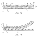
- FIG. 1A is a cross-sectional side view of one embodiment of the tamper indicating security device of the present invention, where the optical film material comprises one focusing element layer, one icon layer, and an optical spacer positioned between and adhered to these layers, the film material being adhered or bonded directly to a base material without using an adhesive;
- FIG. 1B shows interlayer failure between the optical spacer and the icon layer of the tamper indicating security device shown in FIG. 1A , as an attempt is made to detach the device from the base material;
- FIG. 2A is similar to FIG. 1A except that the focusing element layer is an embedded layer of convex lenses;
- FIG. 2B shows interlayer failure between the focusing element layer and optical spacer of the tamper indicating security device of FIG. 2A
- FIG. 2C shows interlayer failure between the optical spacer and icon layer
- FIG. 3A is also similar to FIG. 1A except that the focusing element layer is an embedded layer of concave lenses;
- FIG. 3B shows interlayer failure between the focusing element layer and optical spacer of the tamper indicating security device of FIG. 3A
- FIG. 3C shows interlayer failure between the optical spacer and icon layer
- FIG. 4A is also similar to FIG. 1A except that the focusing element layer is an embedded layer of convex gradient-index (GRIN) lenses;
- GRIN convex gradient-index
- FIG. 4B shows interlayer failure between the focusing element layer and optical spacer of the tamper indicating security device of FIG. 4A
- FIG. 4C shows interlayer failure between the optical spacer and icon layer
- FIG. 5A is a cross-sectional side view of yet another embodiment of the tamper indicating security device of the present invention, where the optical film material comprises one focusing element layer, one icon layer, and two optical spacers adhered together by a primer or adhesive layer, the two optical spacers positioned between and adhered to the focusing element layer and the icon layer, the film material being adhered or bonded directly to a base material without using an adhesive;
- FIG. 5B shows interlayer failure between one optical spacer and the primer or adhesive layer of the tamper indicating security device shown in FIG. 5A ;
- FIG. 6A is similar to FIG. 5A except that the focusing element layer is an embedded layer of convex lenses;
- FIG. 6B shows interlayer failure between one optical spacer and the primer or adhesive layer of the tamper indicating security device shown in FIG. 6A ;
- FIG. 7 is a cross-sectional side view of another embodiment of the inventive tamper indicating security device, where the optical film material comprises one focusing element layer, one icon layer, an optical spacer positioned between and adhered to the focusing element layer and the icon layer, a stiffening layer applied to the underside of the icon layer to promote failure between the optical spacer and the icon layer, and an adhesive layer, the adhesive layer serving to adhere or bond the film material to a base material; and
- FIG. 8 is a cross-sectional side view of yet another embodiment of the tamper indicating security device of the present invention, where the optical film material comprises a layer of metalized focusing reflectors (instead of refractive lenses), an icon layer, an optical spacer or spacer layer located between the focusing reflector layer and the icon layer, and an adhesive layer, which embeds the focusing reflector layer and as noted above serves to adhere or bond the film material to a base material.
- the optical film material comprises a layer of metalized focusing reflectors (instead of refractive lenses), an icon layer, an optical spacer or spacer layer located between the focusing reflector layer and the icon layer, and an adhesive layer, which embeds the focusing reflector layer and as noted above serves to adhere or bond the film material to a base material.
- the present inventors recognizing the usefulness of a “peel to destroy” feature, have developed a tamper indicating security device designed for intralayer and/or interlayer failure when an attempt is made to separate the device from an underlying base material.
- the inventive device which can take the form of, for example, a security strip, thread, patch, inlay, or overlay, is contemplated for use with, among other things, currency or banknotes, secure documents such as bonds, checks, travelers checks, identification cards, lottery tickets, passports, postage stamps, and stock certificates, as well as non-secure documents such as stationery items and labels.
- the inventive device is also contemplated for use with consumer goods as well as bags or packaging used with consumer goods.
- Device 10 basically comprises: a optical film material 12 made up of a layer containing focusing elements 14 , a layer containing icons 16 , and an optical spacer 18 , which is positioned between and adhered to the focusing element layer 14 and the icon layer 16 , the focusing elements forming at least one synthetic image 20 of at least a portion of the icons.
- a synthetic image may operate to modulate or control the extent of the appearance of another synthetic image, as described in U.S. Pat. No. 7,738,175, which is incorporated herein by reference in its entirety.
- the inventive tamper indicating optical security device 10 is shown directly adhered to base material 22 by, for example, using heat to seal or fuse the materials together, using pressure sensitive adhesive materials, or forming interlocking microstructures.
- FIGS. 2A , 3 A, 4 A depict embodiments similar to the embodiment shown in FIG. 1A , with the exception that: the focusing element layer 14 is an embedded layer of convex lenses 24 in FIG. 2A , with reference numeral 26 used to designate the embedding material; the focusing element layer 14 is an embedded layer of concave lenses 28 in FIG. 3A ; and the focusing element layer 14 is an embedded layer of convex gradient-index (GRIN) lenses 30 in FIG. 4A .
- GRIN convex gradient-index
- FIGS. 5A , 6 A depict embodiments of the tamper indicating security device 10 of the present invention, where the optical film material 12 comprises one focusing element layer 14 (an embedded focusing element layer being shown in FIG. 6A ), one icon layer 16 , and two optical spacers 18 a , 18 b , adhered together by a primer or adhesive layer 32 , the two optical spacers 18 a , 18 b , positioned between and adhered to the focusing element layer 14 and the icon layer 16 , the film material being adhered or bonded directly to a base material 22 without using an adhesive.
- the optical film material 12 comprises one focusing element layer 14 (an embedded focusing element layer being shown in FIG. 6A ), one icon layer 16 , and two optical spacers 18 a , 18 b , adhered together by a primer or adhesive layer 32 , the two optical spacers 18 a , 18 b , positioned between and adhered to the focusing element layer 14 and the icon layer 16 , the film material being
- the focusing elements of focusing element layer 14 can be either refractive focusing elements, reflective focusing elements, or hybrid refractive/reflective focusing elements.
- the focusing elements can be an array of refractive micro-lenses. Examples of suitable focusing elements are disclosed in U.S. Pat. No. 7,333,268 to Steenblik et al., U.S. Pat. No. 7,468,842 to Steenblik et al., and U.S. Pat. No. 7,738,175 to Steenblik et al., all of which, as noted above, are fully incorporated by reference as if fully set forth herein.
- the focusing element layer 14 may be either partially or totally embedded, with partial or total embedment of this layer serving to improve the inventive security device's resistance to optically degrading external effects.
- the refractive index from an outer surface of the inventive device to refracting interfaces is varied between a first and a second refractive index, the first refractive index being substantially or measurably different than the second refractive index.
- substantially or measurably different means a difference in refractive index that causes the focal length(s) of the focusing elements to change at least about 0.1 micron.
- the variation of the refractive index may be achieved using a material (hereinafter referred to as “the second material”) that either (i) fills interstitial spaces between at least a portion of the focusing elements and/or covers these focusing elements, forming a distinct interface with the material used to form the focusing elements (hereinafter referred to as “the first material”), or (ii) diffuses into the first material thereby forming a gradient interface with the first material.
- the second material may either partially or totally embed the focusing element layer or may encapsulate the inventive device. More preferably, the second material either forms an outer boundary of the focusing element layer (total embedment of the focusing element layer), or forms an outer boundary of both the focusing element and icon layers (total encapsulation of the tamper indicating security device).
- the second material may be transparent, translucent, tinted, or pigmented and may provide additional functionality for security and authentication purposes, including support of automated currency authentication, verification, tracking, counting and detection systems, that rely on optical effects, electrical conductivity or electrical capacitance, magnetic field detection.
- Suitable materials can include adhesives, gels, glues, lacquers, liquids, molded polymers, and polymers or other materials containing organic or metallic dispersions.
- the icons of icon layer 16 can be either positive or negative icon elements. Further the icon elements can be formed using a number of different techniques. For example, the icon elements can be formed by thermoforming, casting, compression molding, injection molding, embossing, patterned radiation exposure and development, laser exposure and development, ink-jet printing, electro printing, printing, engraving, electroforming, photographic, holographic, and laser exposure of a photosensitive emulsion combined with well-known hardening and etching or swelling processes, masking and deposition processes, masking and chemical etching, masking and reactive ion etching, masking and ion beam milling, micromachining, laser machining and laser ablation, photopolymer exposure and development, and other suitable means and combinations thereof.
- the icon elements are microstructures in the form of voids or recesses in a polymeric substrate, or their inverse shaped posts, with the voids (or recesses) or regions surrounding the shaped posts optionally filled with a contrasting substance such as dyes, coloring agents, pigments, powdered materials, inks, powdered minerals, metal materials and particles, magnetic materials and particles, magnetized materials and particles, magnetically reactive materials and particles, phosphors, liquid crystals, liquid crystal polymers, carbon black or other light absorbing materials, titanium dioxide or other light scattering materials, photonic crystals, non-linear crystals, nanoparticles, nanotubes, buckeyballs, buckeytubes, organic materials, pearlescent materials, powdered pearls, multilayer interference materials, opalescent materials, iridescent materials, low refractive index materials or powders, high refractive index materials or powders, diamond powder, structural color materials, polarizing materials, polarization rotating materials, fluorescent materials, phosphorescent materials, thermochromic
- Optical spacer or spacer layer 18 is included between focusing element layer 14 and icon layer 16 .
- optical spacer or spacer layer 18 is bonded to or formed as a part of the focusing element layer 14 , or the icon layer 16 .
- the thickness of the focusing element layer 14 is increased to allow the focusing elements to be free standing.
- an optical spacer or spacer layer 18 a is bonded to another optical spacer or spacer layer 18 b .
- interlayer failure can be designed to occur, for example, between the optical spacer or spacer layer 18 and the icon layer 16 , between the focusing element layer 14 and the optical spacer or spacer layer 18 , between the optical spacer or spacer layers 18 a , 18 b , or between the optical spacer or spacer layer 18 containing the focusing elements on one side and the optical spacer or spacer layer containing the icon elements on the opposing side.
- Optical spacer or spacer layer 18 may be formed using one or more essentially transparent or translucent polymers including, but not limited to, polycarbonate, polyester, polyethylene, polyethylene napthalate, polyethylene terephthalate, polypropylene, polyvinylidene chloride, and the like.
- the optical spacer or spacer layer(s) 18 is formed using polyester or polyethylene terephthalate.
- the tamper indicating security device 10 of the present invention may further comprise additional features, such as those described in U.S. Pat. No. 7,333,268 to Steenblik et al., U.S. Pat. No. 7,468,842 to Steenblik et al., and U.S. Pat. No. 7,738,175 to Steenblik et al., all of which, as noted above, are fully incorporated herein by reference as if fully set forth herein.
- security device 10 may optionally further comprise one or more layers such as print layers, metalized or partially metalized layers, primer or adhesive layers, sealing or coating layers, and stiffening layers.
- security device 10 further comprises a sealing or coating layer applied to a side of the icon layer(s) for protecting this layer(s).
- the sealing or coating layer may be transparent, translucent, tinted, pigmented, opaque, metallic, magnetic, optically variable, or any combination of these that provide desirable optical effects and/or additional functionality for security and authentication purposes, including support of automated currency authentication, verification, tracking, counting and detection systems, that rely on optical effects, electrical conductivity or electrical capacitance, magnetic field detection.
- Suitable sealing or coating layer materials can include any of the radiation curable resins listed below, plus many different commercially available paints, inks, overcoats, varnishes, lacquers, and clear coats used in the printing and paper and film converting industries.
- security device 10 is prepared substantially in accordance with the process or processes described in U.S. Pat. No. 7,333,268 to Steenblik et al., U.S. Pat. No. 7,468,842 to Steenblik et al., U.S. Pat. No. 7,738,175 to Steenblik et al.
- security device 10 may be prepared by: (a) applying a substantially transparent or clear radiation curable resin to the upper and lower surfaces of the optical spacer or spacer layer 18 ; (b) forming a microlens array on the upper surface and an icon array in the form of microstructures, for example, recesses and/or shaped posts, on the lower surface of the optical spacer 18 ; (c) curing the substantially transparent or clear resin using a source of radiation; (d) filling the icon array recesses and/or areas surrounding the shaped posts with a pigmented resin or ink; and (e) removing excess resin or ink from the lower surface of the optical spacer 18 .
- Suitable radiation curable resins include, but are not limited to, acrylics, epoxies, polyesters, acrylated polyesters, polypropylenes, urethanes, acrylated urethanes, and the like.
- the arrays are formed using an acrylated urethane, which is available from Lord Chemicals.
- security device 10 may be used for authentication of currency or banknotes, secure documents (e.g., identification (ID) cards) and consumer goods.
- security device 10 may be adhered to any base material that requires a security device, including, but not limited to, materials such as plastics, polymer films (e.g., acrylic, cellophane, polycarbonate, polyester, polyethylene, polypropylene, polyvinyl, polyvinylidene chloride, nylon), leathers, metals, glass, wood, paper or paper-like material, cloth, and the like.
- plastics e.g., acrylic, cellophane, polycarbonate, polyester, polyethylene, polypropylene, polyvinyl, polyvinylidene chloride, nylon
- leathers e.g., metals, glass, wood, paper or paper-like material, cloth, and the like.
- security device 10 is adhered or bonded to a passport paper.
- security device 10 may be adhered or bonded to an underlying base material 22 with or without the use of an adhesive. Bonding without the use of an adhesive may be achieved using, for example, thermal welding techniques such as ultrasonic welding, vibration welding, and laser fusing.
- Adhesives for adhering device 10 to a base material 22 may be one of hot melt adhesives, heat activatable adhesives, pressure sensitive adhesives, and polymeric laminating films. These adhesives are preferably crosslinkable in nature, such as ultraviolet (UV) cured acrylic or epoxy, with crosslinking achieved while the adhesive is in the melt phase, or upon cooling.
- UV ultraviolet
- FIGS. 1B , 2 C, 3 C and 4 C Interlayer failure between the optical spacer or spacer layer 18 and the icon layer 16 of optical film material 12 is shown in FIGS. 1B , 2 C, 3 C and 4 C, as an attempt is made to detach device 10 from base material 22 .
- the sought-after interlayer failure or delamination shown in these drawings may be achieved by:
- interlayer failure between focusing element layer 14 and optical spacer 18 is shown.
- Such interlayer failure or delamination may be achieved by increasing or decreasing the stiffness, bond strength, or crosslink density of the focusing element layer 14 , incorporating stress inducing components into this layer, and/or introducing a bond weakening layer at the interface between layer 14 and optical spacer 18 .
- interlayer failure in FIG. 1B could also have been designed to occur between the focusing element layer 14 and the optical spacer 18 .
- interlayer failure between one optical spacer 18 a and a primer or adhesive layer 32 is shown.
- Such interlayer failure or delamination may be achieved by formulating the primer or adhesive layer 32 so as to reduce its interlayer bond strength so that applied or induced stress is propagated along this plane by, for example, decreasing its stiffness or crosslink density, or by incorporating stress inducing components into the formulation used to prepare this layer.
- interlayer failure or delamination may also be achieved by increasing or decreasing the stiffness, bond strength, or crosslink density of the icon layer 16 .
- Increasing the stiffness and crosslink density of the icon layer 16 may be achieved by, for example, (1) increasing exposure of either the entire security device 10 or just the icon layer 16 to radiation (e.g., UV or electron beam radiation) during manufacture, or (2) increasing exposure of either the entire security device 10 or just the icon layer 16 to radiation once device 10 is in place on base material 22 .
- radiation e.g., UV or electron beam radiation
- interlayer failure is achieved by increasing the time during which the entire film material 12 or device 10 is exposed to radiation.
- the focusing element and icon layers 14 , 16 are usually crosslinkable thermoset layers, while optical spacer 18 is a thermoplastic layer. Increased radiation exposure times will serve to increase the level of crosslinking in these layers to some degree and thus the level of stiffness or Young's modulus (ASTM D747-10, D882-10, or D2240-05 (2010)) and cohesive strength.
- Interlayer failure will occur between the optical spacer or spacer layer 18 and relatively rigid icon layer 16 because the icon layer resists flexing while the focusing element layer 14 is able to flex along with the optical spacer during applied or induced stress (e.g., pressure, flexing, shrinkage).
- stress applied to/induced within film material 12 does not propagate from focusing element to focusing element because of interstitial gaps between the focusing elements which form stress relieving areas.
- the icon layer 16 which is usually a continuous or nearly continuous layer, does propagate stresses into adjacent icon areas thereby increasing the tendency for separation and bond breaking between this layer and a contiguous layer.
- Increased radiation exposure times do not serve to alter the stiffness of the optical spacer, so it retains flexibility relative to the icon layer, increasing the tendency for separation between the layers.
- interlayer failure is achieved by increasing radiation exposure times for just the icon layer 16 .
- selectively increasing exposure of the icon layer 16 to radiation will advantageously prevent degradation or alteration of focusing element layer 14 thereby preserving this layer's good wear and abrasion resistance.
- the stiffness or Young's modulus of the icon layer 16 is greater than the stiffness or Young's modulus of the focusing element layer 14 .
- increasing the stiffness and crosslink density of focusing element layer 14 is preferably achieved by increasing radiation times for just the focusing element layer 14 , while avoiding degradation of the other layers.
- Suitable stiffening layers may be prepared from multifunctional monomers and oligomers including, but not limited to, multifunctional acrylate monomers and oligomers such as polyester tetraacrylate (tensile strength: 6000 psi), bisphenol A epoxy diacrylate (tensile strength: 13,900 psi) and dipropylene glycol diacrylate (tensile strength: 9,100 psi), which are available from Sartomer USA, LLC, 502 Thomas Jones Way, Exton, Pa. 19341, with relative stiffness being controlled by the degree of crosslink density in layer 34 .
- interlayer failure occurs between optical spacer 18 and icon layer 16 of optical film material 12 .
- Interlayer failure may also be achieved by incorporating stress inducing (e.g., volume changing) components into the formulation used to prepare the target layer (e.g., icon layer 16 , or a sealing or coating layer formulation applied to a side of the icon layer 16 ).
- Stress inducing components include, but are not limited to, those components that shrink or evolve gas upon curing (e.g., expanding polyurethane foams), those components that swell when exposed to certain liquids or gases, those components that undergo a phase change or phase separation (e.g., an amorphous polymer that undergoes a phase change to become polycrystalline or crystalline) with a change in temperature.
- the stress inducing components When incorporated into the formulation used to prepare, for example, the icon layer 16 , the stress inducing components cause intrinsic stress in the layer, thereby weakening the bond between the icon layer 16 and a contiguous layer.
- the intrinsically stressed sealing or coating layer When incorporated into the formulation used to prepare the sealing or coating layer formulation, the intrinsically stressed sealing or coating layer will exert a force on the icon layer 16 , which serves to likewise weaken the bond between the icon layer 16 and a contiguous layer.
- the described intralayer failure may also be achieved by introducing a uniform or patterned bond weakening or sacrificial layer (e.g., lacquer or other material having a relatively low cohesive strength such as metal including vapor deposited or sputtered metal, or dielectric materials) at an interface between the focusing element layer 14 and the icon layer 16 .
- Suitable bond weakening or sacrificial layers are prepared using materials having relatively low cohesive strength (i.e., materials where stress causing tensile fracture (without plastic deformation) is relatively low) and include, but are not limited to, lacquers, metal layers (e.g., vapor deposited or sputtered metal layers) and dielectric coatings.
- interlayer failure may be achieved, as best shown in FIG. 8 , by applying a uniform or patterned metal layer 38 to the focusing reflector surface 40 .
- the metal layer 38 serves to improve focusing efficiency while allowing for interlayer failure when an attempt is made to detach device 10 from the underlying base material 22 .
- adhesive material 42 fills interstitial spaces between and covers the focusing reflectors.
- interlayer failure of the device shown in FIG. 8 may also be designed to occur between the icon layer 16 and the optical spacer 18 , or between the optical spacer 18 and the layer of focusing reflectors 40 .
- the described interlayer failure can also be designed to occur between other layers of the system.
- one or more additional focusing element layers can be included, as well as one or more additional icon layers.
- one or more additional synthetic images can be formed.
- the interlayer failure described herein can be designed to occur between layers such that the formation of one, but not the other, of the two synthetic images is disrupted.
- the present invention fulfills its security and tamper indicating functions without requiring major production system changes and/or major fabrication step changes other than, for example, formulation and curing dosage changes.
- the inventive device may be adhered to any base material that requires a security device, this invention is particularly advantageous when used with, for example, identification documents such as passport papers.
- Security particularly at major airports has become a significant concern.
- No printable identification is currently available to positively identify a passenger with high reliability and tamper resistance.
- the present invention serves to increase the level of reliability of passport papers by providing the paper with clear and unmistakable tamper indicating properties.
Abstract
Description
-
- (a) an optical film material comprising at least one layer containing focusing elements, at least one layer containing image elements, and an optical spacer or spacer layer positioned between and adhered to the at least one focusing element layer and the at least one image element layer, with the focusing elements forming one or more synthetic images of at least a portion of the image elements; and
- (b) optionally, one or more layers selected from the group of print layers, metalized and/or partially demetalized layers, primer or adhesive layers, sealing or coating layers, stiffening layers, and combinations thereof.
-
- (a) an optical film material comprising at least one layer containing focusing elements, at least one layer containing image elements, two optical spacer or spacer layers adhered together by a primer or adhesive layer, the two optical spacer or spacer layers positioned between and adhered to the at least one focusing element layer and the at least one image element layer, with the focusing elements forming one or more synthetic images of at least a portion of the image elements; and
- (b) optionally, one or more layers selected from the group of print layers, metalized and/or partially demetalized layers, primer or adhesive layers, sealing or coating layers, stiffening layers, and combinations thereof.
-
- (a) the cohesive strength of a target layer in the security device is less than the cohesive strength of the other layers in the security device; and/or
- (b) the bond strength of a target interface between two layers in the security device is less than the bond strength(s) of the interface(s) between other layers in the security device and between the security device and the base material.
-
- (1) increasing or decreasing the stiffness (Young's modulus or tensile modulus), bond strength, or crosslink density of one or more target layers or interfaces relative to the remaining layers or interfaces of the security device;
- (2) incorporating stress inducing (e.g., volume changing) components into one or more target layers of the security device; and/or
- (3) introducing a bond weakening layer at a target interface between two layers of the security device.
-
- (1) increasing or decreasing the stiffness (Young's modulus or tensile modulus), bond strength, or crosslink density of the
icon layer 16; - (2) incorporating stress inducing (e.g., volume changing) components into either the icon layer formulation or a sealing or coating layer formulation applied to a side of the
icon layer 16; and/or - (3) introducing a bond weakening or sacrificial layer at an interface between the optical spacer or
spacer layer 18 and theicon layer 16.
- (1) increasing or decreasing the stiffness (Young's modulus or tensile modulus), bond strength, or crosslink density of the
Claims (81)
Priority Applications (1)
| Application Number | Priority Date | Filing Date | Title |
|---|---|---|---|
| US12/855,309 US8773763B2 (en) | 2003-11-21 | 2010-08-12 | Tamper indicating optical security device |
Applications Claiming Priority (8)
| Application Number | Priority Date | Filing Date | Title |
|---|---|---|---|
| US52428103P | 2003-11-21 | 2003-11-21 | |
| US53839204P | 2004-01-22 | 2004-01-22 | |
| US62723404P | 2004-11-12 | 2004-11-12 | |
| US10/995,859 US7333268B2 (en) | 2003-11-21 | 2004-11-22 | Micro-optic security and image presentation system |
| US11/771,623 US8120855B2 (en) | 2003-11-21 | 2007-06-29 | Micro-optic security and image presentation system for a security device |
| US11/932,468 US8111462B2 (en) | 2003-11-21 | 2007-10-31 | Micro-optic security and image presentation system |
| US23326409P | 2009-08-12 | 2009-08-12 | |
| US12/855,309 US8773763B2 (en) | 2003-11-21 | 2010-08-12 | Tamper indicating optical security device |
Related Parent Applications (1)
| Application Number | Title | Priority Date | Filing Date |
|---|---|---|---|
| US11/771,623 Continuation-In-Part US8120855B2 (en) | 2003-11-21 | 2007-06-29 | Micro-optic security and image presentation system for a security device |
Publications (2)
| Publication Number | Publication Date |
|---|---|
| US20110019283A1 US20110019283A1 (en) | 2011-01-27 |
| US8773763B2 true US8773763B2 (en) | 2014-07-08 |
Family
ID=42990359
Family Applications (1)
| Application Number | Title | Priority Date | Filing Date |
|---|---|---|---|
| US12/855,309 Active 2026-09-13 US8773763B2 (en) | 2003-11-21 | 2010-08-12 | Tamper indicating optical security device |
Country Status (14)
| Country | Link |
|---|---|
| US (1) | US8773763B2 (en) |
| EP (3) | EP3626474A1 (en) |
| JP (1) | JP5784015B2 (en) |
| KR (1) | KR101758940B1 (en) |
| CN (1) | CN102497994B (en) |
| AU (1) | AU2010282484B2 (en) |
| BR (1) | BR112012003071B1 (en) |
| CA (1) | CA2769301C (en) |
| ES (1) | ES2788023T3 (en) |
| IL (1) | IL218012A (en) |
| MX (1) | MX2012001784A (en) |
| RU (1) | RU2541433C9 (en) |
| WO (1) | WO2011019912A1 (en) |
| ZA (1) | ZA201200509B (en) |
Cited By (10)
| Publication number | Priority date | Publication date | Assignee | Title |
|---|---|---|---|---|
| WO2018035126A1 (en) | 2016-08-15 | 2018-02-22 | Visual Physics, Llc | Anti-harvestable security feature |
| WO2018148688A1 (en) | 2017-02-10 | 2018-08-16 | Crane & Co., Inc. | Authentication and anti-harvesting security feature with machine detectable indicia |
| US10252563B2 (en) | 2015-07-13 | 2019-04-09 | Wavefront Technology, Inc. | Optical products, masters for fabricating optical products, and methods for manufacturing masters and optical products |
| US10850550B2 (en) | 2016-04-22 | 2020-12-01 | Wavefront Technology, Inc. | Optical switch devices |
| US10859851B2 (en) | 2014-10-24 | 2020-12-08 | Wavefront Technology, Inc. | Optical products, masters for fabricating optical products, and methods for manufacturing masters and optical products |
| CN111746171B (en) * | 2019-03-29 | 2021-06-15 | 中钞特种防伪科技有限公司 | Optical anti-counterfeiting element and manufacturing method thereof |
| US11113919B2 (en) | 2017-10-20 | 2021-09-07 | Wavefront Technology, Inc. | Optical switch devices |
| US11221448B2 (en) | 2019-04-19 | 2022-01-11 | Wavefront Technology, Inc. | Animated optical security feature |
| US11942344B2 (en) | 2020-09-25 | 2024-03-26 | Samsung Electronics Co., Ltd. | Method of determining a critical temperature of a semiconductor package and apparatus for performing the same |
| US11945253B2 (en) | 2019-05-20 | 2024-04-02 | Crane & Co., Inc. | Use of nanoparticles to tune index of refraction of layers of a polymeric matrix to optimize microoptic (MO) focus |
Families Citing this family (53)
| Publication number | Priority date | Publication date | Assignee | Title |
|---|---|---|---|---|
| US8867134B2 (en) | 2003-11-21 | 2014-10-21 | Visual Physics, Llc | Optical system demonstrating improved resistance to optically degrading external effects |
| DE102009035361A1 (en) * | 2009-07-30 | 2011-02-03 | Giesecke & Devrient Gmbh | Security element for an object to be protected and to be protected object with such a security element |
| CN102103275B (en) * | 2009-12-18 | 2013-09-18 | 清华大学 | Thermochromatic element and thermochromatic display device |
| KR102012526B1 (en) | 2011-01-28 | 2019-08-20 | 크레인 앤 코, 인크 | A laser marked device |
| JP5854628B2 (en) * | 2011-04-26 | 2016-02-09 | キヤノン株式会社 | Optical system and optical apparatus using the same |
| EP2726915A1 (en) * | 2011-06-28 | 2014-05-07 | Visual Physics, LLC | Low curl or curl free optical film-to-paper laminate |
| JP2014524600A (en) * | 2011-08-19 | 2014-09-22 | ビジュアル フィジクス エルエルシー | Optical system capable of transfer on demand with reduced thickness |
| FR2979734B1 (en) * | 2011-09-02 | 2014-05-23 | Arjowiggins Security | SECURITY STRUCTURE COMPRISING A REFLECTIVE OPTICAL STRUCTURE AND ASSOCIATED METHOD. |
| US10195891B2 (en) * | 2011-09-26 | 2019-02-05 | Crane Security Technologies, Inc. | Method for producing a composite web and security devices prepared from the composite web |
| DE102011117677A1 (en) * | 2011-11-04 | 2013-05-08 | Giesecke & Devrient Gmbh | Optically variable security element |
| US10393885B2 (en) * | 2012-06-20 | 2019-08-27 | Battelle Memorial Institute | Gamma radiation stand-off detection, tamper detection, and authentication via resonant meta-material structures |
| US10725208B2 (en) | 2012-06-20 | 2020-07-28 | Battelle Memorial Institute | Two dimensional meta-material windows |
| ES2959465T3 (en) | 2012-08-17 | 2024-02-26 | Visual Physics Llc | A procedure for transferring microstructures to a final substrate |
| AU2014228012B2 (en) | 2013-03-15 | 2018-07-26 | Visual Physics, Llc | Optical security device |
| US9873281B2 (en) | 2013-06-13 | 2018-01-23 | Visual Physics, Llc | Single layer image projection film |
| US20150140536A1 (en) * | 2013-11-15 | 2015-05-21 | Gregory R. Jordan | Flexible optical film material and method for simulating one of a multiplicity of opthalmic conditions representative of a disease state |
| BR112016021736A2 (en) | 2014-03-27 | 2017-08-15 | Visual Physics Llc | OPTICAL DEVICE PRODUCING SPARKLING-TYPE OPTICAL EFFECTS |
| US10766292B2 (en) | 2014-03-27 | 2020-09-08 | Crane & Co., Inc. | Optical device that provides flicker-like optical effects |
| RU2557746C1 (en) * | 2014-04-07 | 2015-07-27 | Виталий Георгиевич Савиновский | Postage stamp with invisible thread "novelty" of savinovsky v.g |
| EP3287295A1 (en) | 2014-07-17 | 2018-02-28 | Visual Physics, LLC | An improved polymeric sheet material for use in making polymeric security documents such as bank notes |
| JP6319692B2 (en) * | 2014-09-08 | 2018-05-09 | 独立行政法人 国立印刷局 | Paper for preventing peeling of valuable media |
| US10195890B2 (en) | 2014-09-16 | 2019-02-05 | Crane Security Technologies, Inc. | Secure lens layer |
| US20160121640A1 (en) * | 2014-11-04 | 2016-05-05 | Lumenco, Llc | Flat concave micro lens for security as an integrated focusing element |
| US10318962B2 (en) | 2014-11-17 | 2019-06-11 | Amazon Technologies, Inc. | Authenticity label for items |
| US10102532B2 (en) * | 2014-11-17 | 2018-10-16 | Amazon Technologies, Inc. | Tracking and verifying authenticity of items |
| CN104698516B (en) * | 2015-02-03 | 2016-08-24 | 兰州大学 | The preparation method of curved compound eye lens arra |
| JP6947358B2 (en) | 2015-02-11 | 2021-10-13 | クレイン アンド カンパニー、 インコーポレイテッド | How to attach the surface of the security device to the board |
| US11143794B2 (en) | 2015-07-08 | 2021-10-12 | Shine Optoelectronics (Kunshan) Co., Ltd | Optical film |
| MA42899A (en) | 2015-07-10 | 2018-05-16 | De La Rue Int Ltd | PROCESSES FOR MANUFACTURING SAFETY DOCUMENTS AND SAFETY DEVICES |
| US9916778B2 (en) * | 2015-08-06 | 2018-03-13 | Xerox Corporation | Backlighting effect for package displays |
| DE102015015991A1 (en) * | 2015-12-10 | 2017-06-14 | Giesecke & Devrient Gmbh | Security element with lenticular image |
| GB2549779B (en) * | 2016-04-29 | 2020-05-20 | De La Rue Int Ltd | Security elements and methods of manufacture thereof |
| RU2736014C2 (en) * | 2016-06-14 | 2020-11-11 | Роллинг Оптикс Инновейшн АБ | Synthetic image and method of its manufacturing |
| US11590791B2 (en) | 2017-02-10 | 2023-02-28 | Crane & Co., Inc. | Machine-readable optical security device |
| US11493673B2 (en) * | 2017-06-29 | 2022-11-08 | 3M Innovative Properties Company | Article and methods of making the same |
| JP7302828B2 (en) | 2018-01-03 | 2023-07-04 | ビジュアル フィジクス エルエルシー | Micro-optical security device with interactive dynamic security features |
| EP3536514A1 (en) | 2018-03-08 | 2019-09-11 | Thales Dis France SA | Cover sheet, security document and method of manufacturing a security document |
| GB201807979D0 (en) * | 2018-05-16 | 2018-07-04 | Optrical Ltd | Improvements in and relating to tamper-evident devices |
| TWI746193B (en) * | 2018-05-17 | 2021-11-11 | 美商伊英克加利福尼亞有限責任公司 | Electro-optic display |
| US11060945B2 (en) * | 2018-05-22 | 2021-07-13 | Paxxus, Inc. | Ultra-violet fluorescing sealant |
| EP3817928A4 (en) * | 2018-07-03 | 2022-03-30 | Crane & Co., Inc. | Security document with attached security device which demonstrates increased harvesting resistance |
| CN111079205B (en) * | 2018-10-22 | 2022-06-21 | 南宁富联富桂精密工业有限公司 | Anti-dismantling mechanism and electronic device with same |
| KR102509867B1 (en) * | 2018-12-21 | 2023-03-13 | 한국조폐공사 | Security sheet comprising watermark |
| GB2584597B (en) * | 2019-03-28 | 2023-01-18 | De La Rue Int Ltd | Security device and method of manufacture thereof |
| CN109870821A (en) * | 2019-04-03 | 2019-06-11 | 冯煜 | A kind of focusing structure and the method for realizing naked eye 3D display |
| KR102183210B1 (en) * | 2019-04-24 | 2020-11-25 | 한국조폐공사 | Security feature manufactured by lamination, the manufacturing method and apparatus of the same |
| GB201913913D0 (en) * | 2019-09-26 | 2019-11-13 | Optrical Ltd | Improvements in and relating to security devices |
| MX2022007751A (en) * | 2019-12-23 | 2022-08-15 | Crane & Co Inc | Ultrasonic bonding of security device to a substrate to prevent harvesting. |
| CN111627145B (en) * | 2020-05-19 | 2022-06-21 | 武汉卓目科技有限公司 | Method and device for identifying fine hollow image-text of image |
| GB202013471D0 (en) * | 2020-08-27 | 2020-10-14 | Ams Int Ag | Moisture-resistant optical device and method of manufacture |
| KR102483935B1 (en) * | 2021-05-06 | 2023-01-04 | 주식회사 윈글로벌 | Optical security labels for preventing counterfeit and method for bonding thereof |
| DE102022109850A1 (en) * | 2022-04-25 | 2023-10-26 | Ovd Kinegram Ag | Laminate and process for producing a laminate |
| KR102541948B1 (en) * | 2022-11-22 | 2023-06-13 | 주식회사 엘티전자 | Luminous textiles with layering method and manufacturing method thereof |
Citations (196)
| Publication number | Priority date | Publication date | Assignee | Title |
|---|---|---|---|---|
| US992151A (en) | 1909-02-04 | 1911-05-16 | Rodolphe Berthon | Apparatus for color photography. |
| US1824353A (en) | 1926-12-15 | 1931-09-22 | Jensen Rasmus Olaf Jonas | Screen for showing projected images in lighted rooms and for shortexposure photography |
| US1849036A (en) | 1926-12-23 | 1932-03-08 | Victor C Ernst | Photographic process and auxiliary element therefor |
| US1942841A (en) | 1931-01-19 | 1934-01-09 | Shimizu Takeo | Daylight screen |
| US2268351A (en) | 1938-08-25 | 1941-12-30 | Tanaka Nawokich | Means for presenting pictures in apparent three dimensions |
| US2355902A (en) | 1941-04-10 | 1944-08-15 | Photoplating Company | Sign with animated effect |
| US2432896A (en) | 1945-03-12 | 1947-12-16 | Hotchner Fred | Retroreflective animation display |
| US2888855A (en) | 1956-08-23 | 1959-06-02 | Tanaka Nawokich | Means for presenting pictures in three dimensional effect |
| US2992103A (en) | 1955-03-29 | 1961-07-11 | Polaroid Corp | Photographic transfer-reversal processes utilizing screen members |
| US3122853A (en) | 1961-08-10 | 1964-03-03 | John C Koonz | Fishing lure |
| US3241429A (en) | 1962-05-14 | 1966-03-22 | Pid Corp | Pictorial parallax panoramagram units |
| US3264164A (en) | 1962-04-30 | 1966-08-02 | Toscony Inc | Color dynamic, three-dimensional flexible film and method of making it |
| US3312006A (en) | 1964-03-11 | 1967-04-04 | Rowland Products Inc | Motion displays |
| US3357772A (en) | 1963-02-27 | 1967-12-12 | Rowland Products Inc | Phased lenticular sheets for optical effects |
| GB1095286A (en) | 1963-07-08 | 1967-12-13 | Portals Ltd | Security device for use in security papers |
| US3463581A (en) | 1966-01-17 | 1969-08-26 | Intermountain Res & Eng | System for three-dimensional panoramic static-image motion pictures |
| US3609035A (en) | 1968-12-30 | 1971-09-28 | Ricoh Kk | Method and device for recording characters or symbols in a reproducibly indiscernible manner |
| US3643361A (en) | 1969-11-17 | 1972-02-22 | Photo Motion Corp | Moire motion illusion apparatus |
| US3704068A (en) | 1971-04-21 | 1972-11-28 | Personal Communications Inc | Micro-image recording and read-out system |
| US3811213A (en) | 1968-11-17 | 1974-05-21 | Photo Motion Corp | Moire motion illusion apparatus and method |
| US3887742A (en) | 1972-04-13 | 1975-06-03 | Richard E Reinnagel | Copy resistant documents |
| US4025673A (en) | 1972-04-13 | 1977-05-24 | Reinnagel Richard E | Method of forming copy resistant documents by forming an orderly array of fibers extending upward from a surface, coating the fibers and printing the coated fibers and the copy resistant document resulting from said method |
| US4073650A (en) | 1974-05-30 | 1978-02-14 | Izon Corporation | Method of recording on a microfiche |
| US4082426A (en) | 1976-11-26 | 1978-04-04 | Minnesota Mining And Manufacturing Company | Retroreflective sheeting with retroreflective markings |
| US4185191A (en) | 1978-06-05 | 1980-01-22 | Honeywell Inc. | Range determination system |
| US4345833A (en) | 1981-02-23 | 1982-08-24 | American Optical Corporation | Lens array |
| EP0090130A1 (en) | 1982-03-25 | 1983-10-05 | Billett-Automation Dipl.-Ing. Klaus Schwarz OHG | Process for checking the authenticity of security documents, and distributing device for carrying out the process |
| US4417784A (en) | 1981-02-19 | 1983-11-29 | Rca Corporation | Multiple image encoding using surface relief structures as authenticating device for sheet-material authenticated item |
| US4498736A (en) | 1981-02-02 | 1985-02-12 | Griffin Robert B | Method and apparatus for producing visual patterns with lenticular sheets |
| US4507349A (en) | 1983-05-16 | 1985-03-26 | Howard A. Fromson | Security medium and secure articles and methods of making same |
| US4534398A (en) | 1984-04-30 | 1985-08-13 | Crane & Co. | Security paper |
| US4634220A (en) | 1983-02-07 | 1987-01-06 | Minnesota Mining And Manufacturing Company | Directionally imaged sheeting |
| US4645301A (en) | 1983-02-07 | 1987-02-24 | Minnesota Mining And Manufacturing Company | Transparent sheet containing authenticating image and method of making same |
| US4662651A (en) | 1985-05-31 | 1987-05-05 | The Standard Register Company | Document protection using multicolor characters |
| US4688894A (en) | 1985-05-13 | 1987-08-25 | Minnesota Mining And Manufacturing Company | Transparent retroreflective sheets containing directional images and method for forming the same |
| US4756972A (en) | 1984-03-19 | 1988-07-12 | U.S. Philips Corp. | Laminated optical component |
| US4765656A (en) | 1985-10-15 | 1988-08-23 | Gao Gesellschaft Fur Automation Und Organisation Mbh | Data carrier having an optical authenticity feature and methods for producing and testing said data carrier |
| US4814594A (en) | 1982-11-22 | 1989-03-21 | Drexler Technology Corporation | Updatable micrographic pocket data card |
| US4892385A (en) | 1981-02-19 | 1990-01-09 | General Electric Company | Sheet-material authenticated item with reflective-diffractive authenticating device |
| US4892336A (en) | 1986-03-18 | 1990-01-09 | Gao Gesellschaft Fuer Automation Und Organisation Mbh | Antifalsification document having a security thread embedded therein and a method for producing the same |
| US4920039A (en) | 1986-01-06 | 1990-04-24 | Dennison Manufacturing Company | Multiple imaging |
| US4935335A (en) | 1986-01-06 | 1990-06-19 | Dennison Manufacturing Company | Multiple imaging |
| US4988126A (en) | 1987-12-04 | 1991-01-29 | Gao Gesellschaft Fur Automation Und Organisation Mbh | Document with an unforgeable surface |
| EP0253089B1 (en) | 1986-07-10 | 1991-09-11 | Landis & Gyr Betriebs AG | Multi-layer document |
| US5074649A (en) | 1989-07-25 | 1991-12-24 | Nippon Sheet Glass Co., Ltd. | Plate with lens array |
| US5085514A (en) | 1989-08-29 | 1992-02-04 | American Bank Note Holographics, Inc. | Technique of forming a separate information bearing printed pattern on replicas of a hologram or other surface relief diffraction pattern |
| EP0319157B1 (en) | 1987-12-04 | 1992-07-29 | Portals Limited | Security paper for bank notes and the like |
| JPH04234699A (en) | 1991-01-08 | 1992-08-24 | Victor Co Of Japan Ltd | Optical card |
| US5211424A (en) | 1991-08-15 | 1993-05-18 | Prc Inc. | Secure passport document and method of making the same |
| US5215864A (en) | 1990-09-28 | 1993-06-01 | Laser Color Marking, Incorporated | Method and apparatus for multi-color laser engraving |
| US5232764A (en) | 1990-06-04 | 1993-08-03 | Meiwa Gravure Co., Ltd. | Synthetic resin pattern sheet |
| US5254390A (en) | 1990-11-15 | 1993-10-19 | Minnesota Mining And Manufacturing Company | Plano-convex base sheet for retroreflective articles and method for making same |
| EP0092691B2 (en) | 1982-04-06 | 1994-04-27 | Kabushiki Kaisha Toshiba | Apparatus for detecting a security thread embedded in a paper-like material |
| US5359454A (en) | 1992-08-18 | 1994-10-25 | Applied Physics Research, L.P. | Apparatus for providing autostereoscopic and dynamic images |
| US5384861A (en) | 1991-06-24 | 1995-01-24 | Picker International, Inc. | Multi-parameter image display with real time interpolation |
| US5393099A (en) | 1993-05-21 | 1995-02-28 | American Bank Note Holographics, Inc. | Anti-counterfeiting laminated currency and method of making the same |
| US5449200A (en) | 1993-06-08 | 1995-09-12 | Domtar, Inc. | Security paper with color mark |
| US5464690A (en) | 1994-04-04 | 1995-11-07 | Novavision, Inc. | Holographic document and method for forming |
| US5479507A (en) | 1994-01-19 | 1995-12-26 | Thomas De La Rue Limited | Copy indicating security device |
| EP0415230B1 (en) | 1989-08-31 | 1996-01-31 | Hughes Aircraft Company | Method for making edge faded holograms |
| US5492370A (en) | 1991-03-22 | 1996-02-20 | De La Rue Holographics Ltd. | Decorative article |
| US5555476A (en) | 1993-08-30 | 1996-09-10 | Toray Industries, Inc. | Microlens array sheet for a liquid crystal display, method for attaching the same and liquid crystal display equipped with the same |
| US5575507A (en) | 1989-01-31 | 1996-11-19 | Dai Nippon Insatsu Kabushiki Kaisha | Heat transfer recording media |
| US5598281A (en) | 1993-11-19 | 1997-01-28 | Alliedsignal Inc. | Backlight assembly for improved illumination employing tapered optical elements |
| US5623368A (en) | 1994-07-07 | 1997-04-22 | Corning Incorporated | Process and apparatus for manufacturing networks of optical microlenses |
| US5623347A (en) | 1991-06-21 | 1997-04-22 | Light Impressions Europe Plc | Holograms for security markings |
| US5626969A (en) | 1992-02-21 | 1997-05-06 | General Binding Corporation | Method of manufacturing film for lamination |
| US5631039A (en) | 1994-08-04 | 1997-05-20 | Portals Limited | Security thread, a film and a method of manufacture of a security thread |
| US5639126A (en) | 1995-06-06 | 1997-06-17 | Crane & Co., Inc. | Machine readable and visually verifiable security threads and security papers employing same |
| US5642226A (en) | 1995-01-18 | 1997-06-24 | Rosenthal; Bruce A. | Lenticular optical system |
| US5688587A (en) | 1993-12-24 | 1997-11-18 | Giesecke & Devrient Gmbh | Antifalsification paper having a thread- or band-shaped security element and a method for producing it |
| US5695346A (en) | 1989-12-07 | 1997-12-09 | Yoshi Sekiguchi | Process and display with moveable images |
| US5712731A (en) | 1993-05-11 | 1998-01-27 | Thomas De La Rue Limited | Security device for security documents such as bank notes and credit cards |
| US5723200A (en) | 1996-02-06 | 1998-03-03 | Meiwa Gravure Co., Ltd. | Decorative sheet |
| US5737126A (en) | 1995-03-08 | 1998-04-07 | Brown University Research Foundation | Microlenses and other optical elements fabricated by laser heating of semiconductor doped and other absorbing glasses |
| RU2111125C1 (en) | 1996-08-14 | 1998-05-20 | Молохина Лариса Аркадьевна | Decorative base for personal visiting, business or identification card, souvenir or congratulatory card, or illustration, or monetary document |
| US5800907A (en) | 1993-09-30 | 1998-09-01 | Grapac Japan Co., Inc. | Method of producing lens method of fabricating article with lens articles with lens resin composition for forming defining lines and lens-forming resin composition |
| US5812313A (en) | 1992-07-23 | 1998-09-22 | Johansen; Frithioff | Method of providing a magnified image of a periodical image pattern |
| US5886798A (en) | 1995-08-21 | 1999-03-23 | Landis & Gyr Technology Innovation Ag | Information carriers with diffraction structures |
| KR100194536B1 (en) | 1996-10-17 | 1999-06-15 | 김충환 | 3D effect handbill and its manufacturing method |
| US5933276A (en) | 1994-04-13 | 1999-08-03 | Board Of Trustees, University Of Arkansas, N.A. | Aberration-free directional image window sheet |
| DE19804858A1 (en) | 1998-01-30 | 1999-08-05 | Ralf Dr Paugstadt | Methods and devices for producing lenticular alternating images |
| US5995638A (en) | 1995-08-28 | 1999-11-30 | Ecole Polytechnique Federale De Lausanne | Methods and apparatus for authentication of documents by using the intensity profile of moire patterns |
| US6036230A (en) | 1994-10-11 | 2000-03-14 | Oesterreichische National Bank | Paper, especially security paper |
| US6036233A (en) | 1995-11-03 | 2000-03-14 | Giesecke & Devrient Gmbh | Data carrier with an optically variable element |
| US6060143A (en) | 1996-11-14 | 2000-05-09 | Ovd Kinegram Ag | Optical information carrier |
| US6089614A (en) | 1996-06-14 | 2000-07-18 | De La Rue International Limited | Security device |
| US6106950A (en) | 1998-06-04 | 2000-08-22 | H. B. Fuller Licesing & Financing Inc. | Waterborne primer and oxygen barrier coating with improved adhesion |
| JP2000256994A (en) | 1999-03-10 | 2000-09-19 | Tokushu Paper Mfg Co Ltd | Windowed thread paper |
| US6176582B1 (en) | 1998-06-12 | 2001-01-23 | 4D-Vision Gmbh | Three-dimensional representation system |
| US6179338B1 (en) | 1992-12-23 | 2001-01-30 | GAO Gesellschaft f{umlaut over (u)}r Automation und Organisation | Compound film for an identity card with a humanly visible authenticity feature |
| US6195150B1 (en) | 1997-07-15 | 2001-02-27 | Silverbrook Research Pty Ltd | Pseudo-3D stereoscopic images and output device |
| JP2001055000A (en) | 1999-06-09 | 2001-02-27 | Yamatsukusu Kk | Virtual image appearing decorative body |
| US6256149B1 (en) | 1998-09-28 | 2001-07-03 | Richard W. Rolfe | Lenticular lens sheet and method of making |
| US6288842B1 (en) | 2000-02-22 | 2001-09-11 | 3M Innovative Properties | Sheeting with composite image that floats |
| US6301363B1 (en) | 1998-10-26 | 2001-10-09 | The Standard Register Company | Security document including subtle image and system and method for viewing the same |
| JP2001324949A (en) | 2000-05-16 | 2001-11-22 | Toppan Printing Co Ltd | Dot pattern display medium as well as method for manufacturing the same, authenticity discrimination method and copying prevention method using the same |
| US20010048968A1 (en) | 2000-02-16 | 2001-12-06 | Cox W. Royall | Ink-jet printing of gradient-index microlenses |
| US6329040B1 (en) | 1997-12-26 | 2001-12-11 | Meiwa Gravure Co., Ltd. | Decorative sheet having three-dimensional effect |
| US6328342B1 (en) | 1995-08-01 | 2001-12-11 | Boris Ilich Belousov | Tape data carrier, method and device for manufacturing the same |
| US6345104B1 (en) | 1994-03-17 | 2002-02-05 | Digimarc Corporation | Digital watermarks and methods for security documents |
| US20020014967A1 (en) | 1997-12-02 | 2002-02-07 | Crane Timothy T. | Security device having multiple security detection features |
| US6348999B1 (en) | 1995-05-10 | 2002-02-19 | Epigem Limited | Micro relief element and preparation thereof |
| US6350036B1 (en) | 1998-10-30 | 2002-02-26 | Avery Dennison Corporation | Retroreflective sheeting containing a validation image and methods of making the same |
| FR2803939B1 (en) | 2000-01-18 | 2002-03-01 | Rexor | SECURITY WIRE OR TRANSFER FILM FOR HOT MARKING FOR BANK NOTES, DOCUMENTS OR OTHER SECURITY ARTICLES |
| US6369947B1 (en) | 1996-12-12 | 2002-04-09 | Ovd Kinegram Ag | Surface pattern |
| US6373965B1 (en) | 1994-06-24 | 2002-04-16 | Angstrom Technologies, Inc. | Apparatus and methods for authentication using partially fluorescent graphic images and OCR characters |
| US6381071B1 (en) | 1999-09-30 | 2002-04-30 | U.S. Philips Corporation | Lenticular device |
| US6424467B1 (en) | 2000-09-05 | 2002-07-23 | National Graphics, Inc. | High definition lenticular lens |
| US6450540B1 (en) | 2000-11-15 | 2002-09-17 | Technology Tree Co., Ltd | Printed matter displaying various colors according to view angle |
| US6467810B2 (en) | 1996-10-10 | 2002-10-22 | Securency Pty Ltd | Self-verifying security documents |
| US6473238B1 (en) | 2000-03-17 | 2002-10-29 | Stephen Daniell | Lens arrays |
| US6500526B1 (en) | 2000-09-28 | 2002-12-31 | Avery Dennison Corporation | Retroreflective sheeting containing a validation image and methods of making the same |
| JP2003039583A (en) | 2001-07-27 | 2003-02-13 | Meiwa Gravure Co Ltd | Decorative sheet |
| US20030031861A1 (en) | 2001-08-11 | 2003-02-13 | Sven Reiter | Label with enhanced anticounterfeiting security |
| US6542646B1 (en) | 1998-07-05 | 2003-04-01 | M. V. T. Multi Vision Technologies Ltd. | Computerized image-processing method |
| JP2003165289A (en) | 2001-11-30 | 2003-06-10 | Nissha Printing Co Ltd | Printed matter with micropattern |
| US6616803B1 (en) | 1998-12-29 | 2003-09-09 | De La Rue International Limited | Making paper |
| US20030179364A1 (en) | 2002-01-24 | 2003-09-25 | Nanoventions, Inc. | Micro-optics for article identification |
| US20030183695A1 (en) | 2001-12-18 | 2003-10-02 | Brian Labrec | Multiple image security features for identification documents and methods of making same |
| CN1126970C (en) | 1996-01-17 | 2003-11-05 | 布鲁斯·A·罗森塔尔 | Lenticular optical system |
| US20030228014A1 (en) | 2002-06-06 | 2003-12-11 | Alasia Alfred V. | Multi-section decoding lens |
| US20030234294A1 (en) | 2002-06-19 | 2003-12-25 | Shinji Uchihiro | Preparing method of IC card and IC card |
| TW575740B (en) | 2001-07-03 | 2004-02-11 | 3M Innovative Properties Co | Sheeting with composite image that floats |
| US6712399B1 (en) | 1999-07-23 | 2004-03-30 | De La Rue International Limited | Security device |
| US6724536B2 (en) | 1990-05-18 | 2004-04-20 | University Of Arkansas | Directional image lenticular window sheet |
| US6726858B2 (en) | 2001-06-13 | 2004-04-27 | Ferro Corporation | Method of forming lenticular sheets |
| GB2362493B (en) | 2000-04-04 | 2004-05-12 | Floating Images Ltd | Advertising hoarding,billboard or poster with high visual impact |
| US20040100707A1 (en) | 2000-06-28 | 2004-05-27 | Ralph Kay | Security device |
| US6751024B1 (en) | 1999-07-22 | 2004-06-15 | Bruce A. Rosenthal | Lenticular optical system |
| US20040140665A1 (en) | 2001-03-27 | 2004-07-22 | Serigraph Inc. | Reflective article and method of manufacturing same |
| US6795250B2 (en) | 2000-12-29 | 2004-09-21 | Lenticlear Lenticular Lens, Inc. | Lenticular lens array |
| JP2004262144A (en) | 2003-03-03 | 2004-09-24 | Dainippon Printing Co Ltd | Validity judgement body and label for validity judgement body |
| US6803088B2 (en) | 2002-10-24 | 2004-10-12 | Eastman Kodak Company | Reflection media for scannable information system |
| US20040209049A1 (en) | 2003-04-17 | 2004-10-21 | Marco Bak | Laser marking in retroreflective security laminate |
| WO2004036507A3 (en) | 2002-10-16 | 2004-11-11 | Ecole Polytech | Authentication of documents and articles by moire patterns |
| US6819775B2 (en) | 1996-07-05 | 2004-11-16 | ECOLE POLYTECHNIQUE FéDéRALE DE LAUSANNE | Authentication of documents and valuable articles by using moire intensity profiles |
| US6833960B1 (en) | 2001-03-05 | 2004-12-21 | Serigraph Inc. | Lenticular imaging system |
| RU2245566C2 (en) | 2002-12-26 | 2005-01-27 | Молохин Илья Валерьевич | Light-reflecting layout material |
| US6856462B1 (en) | 2002-03-05 | 2005-02-15 | Serigraph Inc. | Lenticular imaging system and method of manufacturing same |
| US6870681B1 (en) | 1992-09-21 | 2005-03-22 | University Of Arkansas, N.A. | Directional image transmission sheet and method of making same |
| US20050094274A1 (en) | 2002-04-08 | 2005-05-05 | Hologram Industries (S.A.), A Corporation Of France | Optical security component |
| US20050104364A1 (en) | 2001-12-21 | 2005-05-19 | Giesecke & Devrient Gmbh | Security element for security papers and valuable documents |
| US6900944B2 (en) | 2000-11-02 | 2005-05-31 | Taylor Corporation | Lenticular card and processes for making |
| US20050161501A1 (en) | 2001-12-21 | 2005-07-28 | Giesecke & Devrient Gmbh | Value document and device for processing value documents |
| US6935756B2 (en) | 2002-06-11 | 2005-08-30 | 3M Innovative Properties Company | Retroreflective articles having moire-like pattern |
| DE19932240B4 (en) | 1999-07-10 | 2005-09-01 | Bundesdruckerei Gmbh | Optically variable displayable / concealable security elements for value and security documents |
| US20050247794A1 (en) * | 2004-03-26 | 2005-11-10 | Jones Robert L | Identification document having intrusion resistance |
| US20060003295A1 (en) | 2004-06-30 | 2006-01-05 | Hersch Roger D | Model-based synthesis of band moire images for authenticating security documents and valuable products |
| US20060017979A1 (en) | 2004-07-20 | 2006-01-26 | Pixalen, Llc | Matrical imaging method and apparatus |
| US20060018021A1 (en) | 2004-07-26 | 2006-01-26 | Applied Opsec, Inc. | Diffraction-based optical grating structure and method of creating the same |
| WO2004087430A8 (en) | 2003-04-02 | 2006-03-02 | Ucb Sa | Authentication means |
| US7030997B2 (en) | 2001-09-11 | 2006-04-18 | The Regents Of The University Of California | Characterizing aberrations in an imaging lens and applications to visual testing and integrated circuit mask analysis |
| EP1659449A2 (en) | 2004-11-23 | 2006-05-24 | E.I.Du pont de nemours and company | Low-temperature curable photosensitive compositions |
| US7058202B2 (en) | 2002-06-28 | 2006-06-06 | Ecole polytechnique fédérale de Lausanne (EPFL) | Authentication with built-in encryption by using moire intensity profiles between random layers |
| US7114750B1 (en) | 1995-11-29 | 2006-10-03 | Graphic Security Systems Corporation | Self-authenticating documents |
| US20070058260A1 (en) | 2004-11-22 | 2007-03-15 | Steenblik Richard A | Image presentation and micro-optic security system |
| US20070092680A1 (en) | 2005-10-26 | 2007-04-26 | Sterling Chaffins | Laser writable media substrate, and systems and methods of laser writing |
| US7246824B2 (en) | 2000-06-01 | 2007-07-24 | Optaglio Limited | Labels and method of forming the same |
| US7254265B2 (en) | 2000-04-01 | 2007-08-07 | Newsight Corporation | Methods and systems for 2D/3D image conversion and optimization |
| US20070183047A1 (en) | 2000-01-21 | 2007-08-09 | Jds Uniphase Corporation | Optically Variable Security Devices |
| US7255911B2 (en) | 2000-11-04 | 2007-08-14 | Leonard Durz Gmbh & Co. Kg | Laminate body, in particular a laminate foil and a method of increasing the forgery-proof nature of laminate body |
| US7288320B2 (en) | 2002-05-17 | 2007-10-30 | Nanoventions Holdings, Llc | Microstructured taggant particles, applications and methods of making the same |
| WO2007076952A3 (en) | 2005-12-23 | 2007-11-01 | Giesecke & Devrient Gmbh | Security element |
| US20070273143A1 (en) | 2006-05-12 | 2007-11-29 | Crane Timothy T | Micro-optic film structure that alone or together with a security document or label projects images spatially coordinated with static images and/or other projected images |
| US20070284546A1 (en) | 2001-07-17 | 2007-12-13 | Optaglio Ltd. | Optical device and method of manufacture |
| US20070291362A1 (en) | 2006-06-20 | 2007-12-20 | Applied Opsec, Inc. | Optically variable device with diffraction-based micro-optics, method of creating the same, and article employing the same |
| EP1876028A1 (en) | 2006-07-07 | 2008-01-09 | Setec Oy | Method for producing a data carrier and data carrier produced therefrom |
| US7336422B2 (en) | 2000-02-22 | 2008-02-26 | 3M Innovative Properties Company | Sheeting with composite image that floats |
| US7372631B2 (en) | 2004-09-01 | 2008-05-13 | Seiko Epson Corporation | Method of manufacturing microlens, microlens, microlens array, electro-optical device, and electronic apparatus |
| US20080130018A1 (en) | 2003-05-19 | 2008-06-05 | Nanoventions, Inc. | Microstructured Taggant Particles, Applications and Methods of Making the Same |
| US7389939B2 (en) * | 2003-09-26 | 2008-06-24 | Digimarc Corporation | Optically variable security features having covert forensic features |
| US20080160226A1 (en) | 2005-02-18 | 2008-07-03 | Giesecke & Devriend Gmbh | Security Element and Method for the Production Thereof |
| US20080182084A1 (en) | 2007-01-30 | 2008-07-31 | Ovd Kinegram Ag | Security element for safeguarding value-bearing documents |
| US7422781B2 (en) | 2003-04-21 | 2008-09-09 | 3M Innovative Properties Company | Tamper indicating devices and methods for securing information |
| US7457039B2 (en) | 2006-06-07 | 2008-11-25 | Genie Lens Technologies, Llc | Lenticular display system with a lens sheet spaced apart from a paired interlaced image |
| US7457038B2 (en) | 2003-09-22 | 2008-11-25 | Gene Dolgoff | Omnidirectional lenticular and barrier-grid image displays and methods for making them |
| WO2009000527A1 (en) | 2007-06-25 | 2008-12-31 | Giesecke & Devrient Gmbh | Representation system |
| WO2009000528A1 (en) | 2007-06-25 | 2008-12-31 | Giesecke & Devrient Gmbh | Representation system |
| US20090034082A1 (en) | 2004-04-30 | 2009-02-05 | De La Rue International, Ltd. | Optically Variable Devices |
| US7504147B2 (en) | 2004-07-22 | 2009-03-17 | Avery Dennison Corporation | Retroreflective sheeting with security and/or decorative image |
| US7630954B2 (en) | 2002-08-13 | 2009-12-08 | Giesecke & Devrient Gmbh | Data carrier comprising an optically variable element |
| US20090315316A1 (en) | 2006-07-25 | 2009-12-24 | Ovd Kinegram Ag | Method of generating a laser mark in a security document, and security document of this kind |
| US20100018644A1 (en) | 2008-07-15 | 2010-01-28 | Sacks Andrew B | Method and assembly for personalized three-dimensional products |
| WO2010015383A1 (en) | 2008-08-05 | 2010-02-11 | Giesecke & Devrient Gmbh | Method for producing microlenses |
| US20100068459A1 (en) | 2008-09-12 | 2010-03-18 | Eternal Chemical Co., Ltd. | Optical film |
| US7686187B2 (en) | 2004-08-26 | 2010-03-30 | Scott V. Anderson | Apparatus and method for open thread, reusable, no-waste collapsible tube dispensers with control ribs and/or detent |
| US20100109317A1 (en) | 2007-02-14 | 2010-05-06 | Giesecke & Devrient Gmbh | Embossing lacquer for micro-optical security elements |
| US7712623B2 (en) | 2006-02-06 | 2010-05-11 | Rubbermaid Commercial Products Llc | Receptacle with vent |
| US7763179B2 (en) | 2003-03-21 | 2010-07-27 | Digimarc Corporation | Color laser engraving and digital watermarking |
| US7812935B2 (en) | 2005-12-23 | 2010-10-12 | Ingenia Holdings Limited | Optical authentication |
| US7849993B2 (en) | 2001-12-21 | 2010-12-14 | Giesecke & Devrient Gmbh | Devices and method for the production of sheet material |
| US20100328922A1 (en) | 2009-06-03 | 2010-12-30 | Leonhard Kurz Stiftung & Co. Kg | Security Document |
| EP1356952B1 (en) | 2002-04-11 | 2011-09-28 | Hueck Folien Gesellschaft m.b.H. | Coated supporting substrate with different optical and/or fluorescent characteristics at both sides |
| US20120033305A1 (en) | 2009-03-04 | 2012-02-09 | Securency International Pty Ltd | Methods for producing lens arrays |
| EP2335937B1 (en) | 2009-12-18 | 2013-02-20 | Agfa-Gevaert | Laser markable security film |
Family Cites Families (8)
| Publication number | Priority date | Publication date | Assignee | Title |
|---|---|---|---|---|
| US5135262A (en) * | 1990-06-20 | 1992-08-04 | Alcan International Limited | Method of making color change devices activatable by bending and product thereof |
| US5169707A (en) * | 1991-05-08 | 1992-12-08 | Minnesota Mining And Manufacturing Company | Retroreflective security laminates with dual level verification |
| CN1247359A (en) * | 1999-06-29 | 2000-03-15 | 陈波 | 3D display film for printed articles |
| GB9918617D0 (en) * | 1999-08-07 | 1999-10-13 | Epigem Limited | An optical display composite |
| JP4565482B2 (en) * | 2001-05-30 | 2010-10-20 | 大日本印刷株式会社 | Hologram laminate and hologram label |
| GB0117096D0 (en) * | 2001-07-13 | 2001-09-05 | Qinetiq Ltd | Security label |
| RU2602397C2 (en) | 2003-11-21 | 2016-11-20 | Визуал Физикс, Ллс | Micro-optical safety and image display system |
| CN101563640B (en) | 2006-06-28 | 2011-12-14 | 光学物理有限责任公司 | Image presentation and micro-optic security system |
-
2010
- 2010-08-12 CN CN201080035671.1A patent/CN102497994B/en active Active
- 2010-08-12 AU AU2010282484A patent/AU2010282484B2/en not_active Ceased
- 2010-08-12 BR BR112012003071-0A patent/BR112012003071B1/en not_active IP Right Cessation
- 2010-08-12 ES ES10760147T patent/ES2788023T3/en active Active
- 2010-08-12 KR KR1020127006219A patent/KR101758940B1/en active IP Right Grant
- 2010-08-12 CA CA2769301A patent/CA2769301C/en active Active
- 2010-08-12 EP EP19208286.5A patent/EP3626474A1/en active Pending
- 2010-08-12 JP JP2012524869A patent/JP5784015B2/en active Active
- 2010-08-12 MX MX2012001784A patent/MX2012001784A/en not_active Application Discontinuation
- 2010-08-12 WO PCT/US2010/045318 patent/WO2011019912A1/en active Application Filing
- 2010-08-12 US US12/855,309 patent/US8773763B2/en active Active
- 2010-08-12 EP EP19208283.2A patent/EP3626473A1/en not_active Withdrawn
- 2010-08-12 EP EP10760147.8A patent/EP2464527B1/en active Active
- 2010-08-12 RU RU2012108183/12A patent/RU2541433C9/en active
-
2012
- 2012-01-20 ZA ZA2012/00509A patent/ZA201200509B/en unknown
- 2012-02-09 IL IL218012A patent/IL218012A/en active IP Right Grant
Patent Citations (245)
| Publication number | Priority date | Publication date | Assignee | Title |
|---|---|---|---|---|
| US992151A (en) | 1909-02-04 | 1911-05-16 | Rodolphe Berthon | Apparatus for color photography. |
| US1824353A (en) | 1926-12-15 | 1931-09-22 | Jensen Rasmus Olaf Jonas | Screen for showing projected images in lighted rooms and for shortexposure photography |
| US1849036A (en) | 1926-12-23 | 1932-03-08 | Victor C Ernst | Photographic process and auxiliary element therefor |
| US1942841A (en) | 1931-01-19 | 1934-01-09 | Shimizu Takeo | Daylight screen |
| US2268351A (en) | 1938-08-25 | 1941-12-30 | Tanaka Nawokich | Means for presenting pictures in apparent three dimensions |
| US2355902A (en) | 1941-04-10 | 1944-08-15 | Photoplating Company | Sign with animated effect |
| US2432896A (en) | 1945-03-12 | 1947-12-16 | Hotchner Fred | Retroreflective animation display |
| US2992103A (en) | 1955-03-29 | 1961-07-11 | Polaroid Corp | Photographic transfer-reversal processes utilizing screen members |
| US2888855A (en) | 1956-08-23 | 1959-06-02 | Tanaka Nawokich | Means for presenting pictures in three dimensional effect |
| US3122853A (en) | 1961-08-10 | 1964-03-03 | John C Koonz | Fishing lure |
| US3264164A (en) | 1962-04-30 | 1966-08-02 | Toscony Inc | Color dynamic, three-dimensional flexible film and method of making it |
| US3241429A (en) | 1962-05-14 | 1966-03-22 | Pid Corp | Pictorial parallax panoramagram units |
| US3357772A (en) | 1963-02-27 | 1967-12-12 | Rowland Products Inc | Phased lenticular sheets for optical effects |
| GB1095286A (en) | 1963-07-08 | 1967-12-13 | Portals Ltd | Security device for use in security papers |
| US3312006A (en) | 1964-03-11 | 1967-04-04 | Rowland Products Inc | Motion displays |
| US3463581A (en) | 1966-01-17 | 1969-08-26 | Intermountain Res & Eng | System for three-dimensional panoramic static-image motion pictures |
| US3811213A (en) | 1968-11-17 | 1974-05-21 | Photo Motion Corp | Moire motion illusion apparatus and method |
| US3609035A (en) | 1968-12-30 | 1971-09-28 | Ricoh Kk | Method and device for recording characters or symbols in a reproducibly indiscernible manner |
| US3643361A (en) | 1969-11-17 | 1972-02-22 | Photo Motion Corp | Moire motion illusion apparatus |
| US3704068A (en) | 1971-04-21 | 1972-11-28 | Personal Communications Inc | Micro-image recording and read-out system |
| US3887742A (en) | 1972-04-13 | 1975-06-03 | Richard E Reinnagel | Copy resistant documents |
| US4025673A (en) | 1972-04-13 | 1977-05-24 | Reinnagel Richard E | Method of forming copy resistant documents by forming an orderly array of fibers extending upward from a surface, coating the fibers and printing the coated fibers and the copy resistant document resulting from said method |
| US4073650A (en) | 1974-05-30 | 1978-02-14 | Izon Corporation | Method of recording on a microfiche |
| US4082426A (en) | 1976-11-26 | 1978-04-04 | Minnesota Mining And Manufacturing Company | Retroreflective sheeting with retroreflective markings |
| US4185191A (en) | 1978-06-05 | 1980-01-22 | Honeywell Inc. | Range determination system |
| US4498736A (en) | 1981-02-02 | 1985-02-12 | Griffin Robert B | Method and apparatus for producing visual patterns with lenticular sheets |
| US4417784A (en) | 1981-02-19 | 1983-11-29 | Rca Corporation | Multiple image encoding using surface relief structures as authenticating device for sheet-material authenticated item |
| US4892385A (en) | 1981-02-19 | 1990-01-09 | General Electric Company | Sheet-material authenticated item with reflective-diffractive authenticating device |
| US4345833A (en) | 1981-02-23 | 1982-08-24 | American Optical Corporation | Lens array |
| EP0090130A1 (en) | 1982-03-25 | 1983-10-05 | Billett-Automation Dipl.-Ing. Klaus Schwarz OHG | Process for checking the authenticity of security documents, and distributing device for carrying out the process |
| EP0092691B2 (en) | 1982-04-06 | 1994-04-27 | Kabushiki Kaisha Toshiba | Apparatus for detecting a security thread embedded in a paper-like material |
| US4814594A (en) | 1982-11-22 | 1989-03-21 | Drexler Technology Corporation | Updatable micrographic pocket data card |
| US4634220A (en) | 1983-02-07 | 1987-01-06 | Minnesota Mining And Manufacturing Company | Directionally imaged sheeting |
| US4645301A (en) | 1983-02-07 | 1987-02-24 | Minnesota Mining And Manufacturing Company | Transparent sheet containing authenticating image and method of making same |
| EP0118222B1 (en) | 1983-02-07 | 1987-11-11 | Minnesota Mining And Manufacturing Company | Directionally imaged sheeting |
| US4507349A (en) | 1983-05-16 | 1985-03-26 | Howard A. Fromson | Security medium and secure articles and methods of making same |
| US4756972A (en) | 1984-03-19 | 1988-07-12 | U.S. Philips Corp. | Laminated optical component |
| US4534398A (en) | 1984-04-30 | 1985-08-13 | Crane & Co. | Security paper |
| US4691993A (en) | 1985-05-13 | 1987-09-08 | Minnesota Mining And Manufacturing Company | Transparent sheets containing directional images and method for forming the same |
| US4688894A (en) | 1985-05-13 | 1987-08-25 | Minnesota Mining And Manufacturing Company | Transparent retroreflective sheets containing directional images and method for forming the same |
| EP0203752B1 (en) | 1985-05-13 | 1992-08-05 | Minnesota Mining And Manufacturing Company | Transparent sheet containing directional image information and method for its production |
| US4662651A (en) | 1985-05-31 | 1987-05-05 | The Standard Register Company | Document protection using multicolor characters |
| US4765656A (en) | 1985-10-15 | 1988-08-23 | Gao Gesellschaft Fur Automation Und Organisation Mbh | Data carrier having an optical authenticity feature and methods for producing and testing said data carrier |
| US4920039A (en) | 1986-01-06 | 1990-04-24 | Dennison Manufacturing Company | Multiple imaging |
| US4935335A (en) | 1986-01-06 | 1990-06-19 | Dennison Manufacturing Company | Multiple imaging |
| US4892336A (en) | 1986-03-18 | 1990-01-09 | Gao Gesellschaft Fuer Automation Und Organisation Mbh | Antifalsification document having a security thread embedded therein and a method for producing the same |
| EP0253089B1 (en) | 1986-07-10 | 1991-09-11 | Landis & Gyr Betriebs AG | Multi-layer document |
| US5433807A (en) | 1987-12-04 | 1995-07-18 | Gao Gesellschaft Fur Automation Und Organisation M.B.H. | Method of producing a document with an unforgeable surface relief |
| EP0319157B1 (en) | 1987-12-04 | 1992-07-29 | Portals Limited | Security paper for bank notes and the like |
| EP0318717B1 (en) | 1987-12-04 | 1993-09-01 | GAO Gesellschaft für Automation und Organisation mbH | Document with reliefs against falsification, and method for manufacturing the same |
| US4988126A (en) | 1987-12-04 | 1991-01-29 | Gao Gesellschaft Fur Automation Und Organisation Mbh | Document with an unforgeable surface |
| US5575507A (en) | 1989-01-31 | 1996-11-19 | Dai Nippon Insatsu Kabushiki Kaisha | Heat transfer recording media |
| US5074649A (en) | 1989-07-25 | 1991-12-24 | Nippon Sheet Glass Co., Ltd. | Plate with lens array |
| US5085514A (en) | 1989-08-29 | 1992-02-04 | American Bank Note Holographics, Inc. | Technique of forming a separate information bearing printed pattern on replicas of a hologram or other surface relief diffraction pattern |
| EP0415230B1 (en) | 1989-08-31 | 1996-01-31 | Hughes Aircraft Company | Method for making edge faded holograms |
| US5695346A (en) | 1989-12-07 | 1997-12-09 | Yoshi Sekiguchi | Process and display with moveable images |
| US6724536B2 (en) | 1990-05-18 | 2004-04-20 | University Of Arkansas | Directional image lenticular window sheet |
| US5232764A (en) | 1990-06-04 | 1993-08-03 | Meiwa Gravure Co., Ltd. | Synthetic resin pattern sheet |
| US5215864A (en) | 1990-09-28 | 1993-06-01 | Laser Color Marking, Incorporated | Method and apparatus for multi-color laser engraving |
| US5254390B1 (en) | 1990-11-15 | 1999-05-18 | Minnesota Mining & Mfg | Plano-convex base sheet for retroreflective articles |
| US5254390A (en) | 1990-11-15 | 1993-10-19 | Minnesota Mining And Manufacturing Company | Plano-convex base sheet for retroreflective articles and method for making same |
| US5468540A (en) | 1990-11-15 | 1995-11-21 | Minnesota Mining And Manufacturing Company | Retroreflective article comprising a transparent base sheet and nacreous pigment coating, method for making such a base sheet, and method for making a forming master |
| JPH04234699A (en) | 1991-01-08 | 1992-08-24 | Victor Co Of Japan Ltd | Optical card |
| US5492370A (en) | 1991-03-22 | 1996-02-20 | De La Rue Holographics Ltd. | Decorative article |
| US5623347A (en) | 1991-06-21 | 1997-04-22 | Light Impressions Europe Plc | Holograms for security markings |
| US5384861A (en) | 1991-06-24 | 1995-01-24 | Picker International, Inc. | Multi-parameter image display with real time interpolation |
| US5211424A (en) | 1991-08-15 | 1993-05-18 | Prc Inc. | Secure passport document and method of making the same |
| US5626969A (en) | 1992-02-21 | 1997-05-06 | General Binding Corporation | Method of manufacturing film for lamination |
| US5812313A (en) | 1992-07-23 | 1998-09-22 | Johansen; Frithioff | Method of providing a magnified image of a periodical image pattern |
| US5461495A (en) | 1992-08-18 | 1995-10-24 | Applied Physics Research, L.P. | Apparatus for providing autostereoscopic and dynamic images and method of manufacturing same |
| US5359454A (en) | 1992-08-18 | 1994-10-25 | Applied Physics Research, L.P. | Apparatus for providing autostereoscopic and dynamic images |
| US5568313A (en) | 1992-08-18 | 1996-10-22 | Applied Physics Research, L.P. | Apparatus for providing autostereoscopic and dynamic images and method of manufacturing same |
| US6870681B1 (en) | 1992-09-21 | 2005-03-22 | University Of Arkansas, N.A. | Directional image transmission sheet and method of making same |
| US6179338B1 (en) | 1992-12-23 | 2001-01-30 | GAO Gesellschaft f{umlaut over (u)}r Automation und Organisation | Compound film for an identity card with a humanly visible authenticity feature |
| US5712731A (en) | 1993-05-11 | 1998-01-27 | Thomas De La Rue Limited | Security device for security documents such as bank notes and credit cards |
| US5393099A (en) | 1993-05-21 | 1995-02-28 | American Bank Note Holographics, Inc. | Anti-counterfeiting laminated currency and method of making the same |
| US5449200A (en) | 1993-06-08 | 1995-09-12 | Domtar, Inc. | Security paper with color mark |
| US5555476A (en) | 1993-08-30 | 1996-09-10 | Toray Industries, Inc. | Microlens array sheet for a liquid crystal display, method for attaching the same and liquid crystal display equipped with the same |
| US5800907A (en) | 1993-09-30 | 1998-09-01 | Grapac Japan Co., Inc. | Method of producing lens method of fabricating article with lens articles with lens resin composition for forming defining lines and lens-forming resin composition |
| US5598281A (en) | 1993-11-19 | 1997-01-28 | Alliedsignal Inc. | Backlight assembly for improved illumination employing tapered optical elements |
| US6030691A (en) | 1993-12-24 | 2000-02-29 | Giesecke & Devrient Gmbh | "Antifalsification" paper having a thread or band shaped security element and a method of producing same |
| US5688587A (en) | 1993-12-24 | 1997-11-18 | Giesecke & Devrient Gmbh | Antifalsification paper having a thread- or band-shaped security element and a method for producing it |
| EP0930174B1 (en) | 1993-12-24 | 2003-04-16 | Giesecke & Devrient GmbH | Security paper with thread- or tape-like security element |
| US5479507A (en) | 1994-01-19 | 1995-12-26 | Thomas De La Rue Limited | Copy indicating security device |
| US6345104B1 (en) | 1994-03-17 | 2002-02-05 | Digimarc Corporation | Digital watermarks and methods for security documents |
| US5674580A (en) | 1994-04-04 | 1997-10-07 | Novavision, Inc. | Plastic foil for hot leaf stamping and method for forming |
| US5670003A (en) | 1994-04-04 | 1997-09-23 | Novavision, Inc. | Holographic document and method for forming |
| US5643678A (en) | 1994-04-04 | 1997-07-01 | Novavision, Inc. | Holographic film and method for forming |
| US5753349A (en) | 1994-04-04 | 1998-05-19 | Novavision, Inc. | Document having security image and composite sheet and method for forming |
| US5759683A (en) | 1994-04-04 | 1998-06-02 | Novavision, Inc. | Holographic document with holographic image or diffraction pattern directly embossed thereon |
| US5783017A (en) | 1994-04-04 | 1998-07-21 | Novavision Inc. | Plastic foil for hot leaf stamping and method for forming |
| US5464690A (en) | 1994-04-04 | 1995-11-07 | Novavision, Inc. | Holographic document and method for forming |
| US5810957A (en) | 1994-04-04 | 1998-09-22 | Novavision, Inc. | Method for forming holographic foil |
| US5933276A (en) | 1994-04-13 | 1999-08-03 | Board Of Trustees, University Of Arkansas, N.A. | Aberration-free directional image window sheet |
| US6373965B1 (en) | 1994-06-24 | 2002-04-16 | Angstrom Technologies, Inc. | Apparatus and methods for authentication using partially fluorescent graphic images and OCR characters |
| US5623368A (en) | 1994-07-07 | 1997-04-22 | Corning Incorporated | Process and apparatus for manufacturing networks of optical microlenses |
| US5631039A (en) | 1994-08-04 | 1997-05-20 | Portals Limited | Security thread, a film and a method of manufacture of a security thread |
| US6036230A (en) | 1994-10-11 | 2000-03-14 | Oesterreichische National Bank | Paper, especially security paper |
| US5642226A (en) | 1995-01-18 | 1997-06-24 | Rosenthal; Bruce A. | Lenticular optical system |
| US6084713A (en) | 1995-01-18 | 2000-07-04 | Rosenthal; Bruce A. | Lenticular optical system |
| US6414794B1 (en) | 1995-01-18 | 2002-07-02 | Bruce A. Rosenthal | Lenticular optical system |
| US6256150B1 (en) | 1995-01-18 | 2001-07-03 | Bruce A. Rosenthal | Lenticular optical system having parallel fresnel lenses |
| US5737126A (en) | 1995-03-08 | 1998-04-07 | Brown University Research Foundation | Microlenses and other optical elements fabricated by laser heating of semiconductor doped and other absorbing glasses |
| US6348999B1 (en) | 1995-05-10 | 2002-02-19 | Epigem Limited | Micro relief element and preparation thereof |
| US6671095B2 (en) | 1995-05-10 | 2003-12-30 | Epigem Limited | Micro relief element and preparation thereof |
| US5639126A (en) | 1995-06-06 | 1997-06-17 | Crane & Co., Inc. | Machine readable and visually verifiable security threads and security papers employing same |
| US6328342B1 (en) | 1995-08-01 | 2001-12-11 | Boris Ilich Belousov | Tape data carrier, method and device for manufacturing the same |
| US5886798A (en) | 1995-08-21 | 1999-03-23 | Landis & Gyr Technology Innovation Ag | Information carriers with diffraction structures |
| US5995638A (en) | 1995-08-28 | 1999-11-30 | Ecole Polytechnique Federale De Lausanne | Methods and apparatus for authentication of documents by using the intensity profile of moire patterns |
| US6036233A (en) | 1995-11-03 | 2000-03-14 | Giesecke & Devrient Gmbh | Data carrier with an optically variable element |
| US6283509B1 (en) | 1995-11-03 | 2001-09-04 | Giesecke & Devrient Gmbh | Data carrier with an optically variable element |
| US7114750B1 (en) | 1995-11-29 | 2006-10-03 | Graphic Security Systems Corporation | Self-authenticating documents |
| CN1126970C (en) | 1996-01-17 | 2003-11-05 | 布鲁斯·A·罗森塔尔 | Lenticular optical system |
| US5723200A (en) | 1996-02-06 | 1998-03-03 | Meiwa Gravure Co., Ltd. | Decorative sheet |
| US6089614A (en) | 1996-06-14 | 2000-07-18 | De La Rue International Limited | Security device |
| US6819775B2 (en) | 1996-07-05 | 2004-11-16 | ECOLE POLYTECHNIQUE FéDéRALE DE LAUSANNE | Authentication of documents and valuable articles by using moire intensity profiles |
| RU2111125C1 (en) | 1996-08-14 | 1998-05-20 | Молохина Лариса Аркадьевна | Decorative base for personal visiting, business or identification card, souvenir or congratulatory card, or illustration, or monetary document |
| US20020185857A1 (en) | 1996-10-10 | 2002-12-12 | Securency Pty Ltd | Self-verifying security documents |
| US6467810B2 (en) | 1996-10-10 | 2002-10-22 | Securency Pty Ltd | Self-verifying security documents |
| US6761377B2 (en) | 1996-10-10 | 2004-07-13 | Securency Pty Ltd | Self-verifying security documents |
| KR100194536B1 (en) | 1996-10-17 | 1999-06-15 | 김충환 | 3D effect handbill and its manufacturing method |
| US6060143A (en) | 1996-11-14 | 2000-05-09 | Ovd Kinegram Ag | Optical information carrier |
| US6369947B1 (en) | 1996-12-12 | 2002-04-09 | Ovd Kinegram Ag | Surface pattern |
| US6195150B1 (en) | 1997-07-15 | 2001-02-27 | Silverbrook Research Pty Ltd | Pseudo-3D stereoscopic images and output device |
| US20020014967A1 (en) | 1997-12-02 | 2002-02-07 | Crane Timothy T. | Security device having multiple security detection features |
| US6329040B1 (en) | 1997-12-26 | 2001-12-11 | Meiwa Gravure Co., Ltd. | Decorative sheet having three-dimensional effect |
| DE19804858A1 (en) | 1998-01-30 | 1999-08-05 | Ralf Dr Paugstadt | Methods and devices for producing lenticular alternating images |
| US6106950A (en) | 1998-06-04 | 2000-08-22 | H. B. Fuller Licesing & Financing Inc. | Waterborne primer and oxygen barrier coating with improved adhesion |
| US6176582B1 (en) | 1998-06-12 | 2001-01-23 | 4D-Vision Gmbh | Three-dimensional representation system |
| US6542646B1 (en) | 1998-07-05 | 2003-04-01 | M. V. T. Multi Vision Technologies Ltd. | Computerized image-processing method |
| US6256149B1 (en) | 1998-09-28 | 2001-07-03 | Richard W. Rolfe | Lenticular lens sheet and method of making |
| US6301363B1 (en) | 1998-10-26 | 2001-10-09 | The Standard Register Company | Security document including subtle image and system and method for viewing the same |
| US6350036B1 (en) | 1998-10-30 | 2002-02-26 | Avery Dennison Corporation | Retroreflective sheeting containing a validation image and methods of making the same |
| US6558009B2 (en) | 1998-10-30 | 2003-05-06 | Avery Dennison Corporation | Retroreflective sheeting containing a validation image and methods of making the same |
| EP0997750B1 (en) | 1998-10-30 | 2005-05-04 | Avery Dennison Corporation | Retroreflective sheeting containing a validation image and methods of making the same |
| US6641270B2 (en) | 1998-10-30 | 2003-11-04 | Avery Dennison Corporation | Retroreflective sheeting containing a validation image and methods of making the same |
| US6616803B1 (en) | 1998-12-29 | 2003-09-09 | De La Rue International Limited | Making paper |
| JP2000256994A (en) | 1999-03-10 | 2000-09-19 | Tokushu Paper Mfg Co Ltd | Windowed thread paper |
| JP2001055000A (en) | 1999-06-09 | 2001-02-27 | Yamatsukusu Kk | Virtual image appearing decorative body |
| DE19932240B4 (en) | 1999-07-10 | 2005-09-01 | Bundesdruckerei Gmbh | Optically variable displayable / concealable security elements for value and security documents |
| US6751024B1 (en) | 1999-07-22 | 2004-06-15 | Bruce A. Rosenthal | Lenticular optical system |
| US6712399B1 (en) | 1999-07-23 | 2004-03-30 | De La Rue International Limited | Security device |
| US6381071B1 (en) | 1999-09-30 | 2002-04-30 | U.S. Philips Corporation | Lenticular device |
| FR2803939B1 (en) | 2000-01-18 | 2002-03-01 | Rexor | SECURITY WIRE OR TRANSFER FILM FOR HOT MARKING FOR BANK NOTES, DOCUMENTS OR OTHER SECURITY ARTICLES |
| US20070183047A1 (en) | 2000-01-21 | 2007-08-09 | Jds Uniphase Corporation | Optically Variable Security Devices |
| US20010048968A1 (en) | 2000-02-16 | 2001-12-06 | Cox W. Royall | Ink-jet printing of gradient-index microlenses |
| US20120019607A1 (en) | 2000-02-22 | 2012-01-26 | 3M Innovative Properties Company | Sheeting with composite image that floats |
| US6288842B1 (en) | 2000-02-22 | 2001-09-11 | 3M Innovative Properties | Sheeting with composite image that floats |
| US7336422B2 (en) | 2000-02-22 | 2008-02-26 | 3M Innovative Properties Company | Sheeting with composite image that floats |
| US20130010048A1 (en) | 2000-02-22 | 2013-01-10 | 3M Innovative Properties Company | Sheeting with composite image that floats |
| US7068434B2 (en) | 2000-02-22 | 2006-06-27 | 3M Innovative Properties Company | Sheeting with composite image that floats |
| US8057980B2 (en) | 2000-02-22 | 2011-11-15 | Dunn Douglas S | Sheeting with composite image that floats |
| US20030112523A1 (en) | 2000-03-17 | 2003-06-19 | Stephen Daniell | Lens arrays |
| US6473238B1 (en) | 2000-03-17 | 2002-10-29 | Stephen Daniell | Lens arrays |
| JP2003528349A (en) | 2000-03-17 | 2003-09-24 | ゾグラフ エルエルシー | High clarity lens system |
| US6721101B2 (en) | 2000-03-17 | 2004-04-13 | Zograph, Llc | Lens arrays |
| US6587276B2 (en) | 2000-03-17 | 2003-07-01 | Zograph Llc | Optical reproduction system |
| US7254265B2 (en) | 2000-04-01 | 2007-08-07 | Newsight Corporation | Methods and systems for 2D/3D image conversion and optimization |
| GB2362493B (en) | 2000-04-04 | 2004-05-12 | Floating Images Ltd | Advertising hoarding,billboard or poster with high visual impact |
| JP2001324949A (en) | 2000-05-16 | 2001-11-22 | Toppan Printing Co Ltd | Dot pattern display medium as well as method for manufacturing the same, authenticity discrimination method and copying prevention method using the same |
| US7246824B2 (en) | 2000-06-01 | 2007-07-24 | Optaglio Limited | Labels and method of forming the same |
| US20040100707A1 (en) | 2000-06-28 | 2004-05-27 | Ralph Kay | Security device |
| US6424467B1 (en) | 2000-09-05 | 2002-07-23 | National Graphics, Inc. | High definition lenticular lens |
| US6500526B1 (en) | 2000-09-28 | 2002-12-31 | Avery Dennison Corporation | Retroreflective sheeting containing a validation image and methods of making the same |
| US7545567B2 (en) | 2000-11-02 | 2009-06-09 | Travel Tags, Inc. | Lenticular card and process for making |
| US6900944B2 (en) | 2000-11-02 | 2005-05-31 | Taylor Corporation | Lenticular card and processes for making |
| US7255911B2 (en) | 2000-11-04 | 2007-08-14 | Leonard Durz Gmbh & Co. Kg | Laminate body, in particular a laminate foil and a method of increasing the forgery-proof nature of laminate body |
| US6450540B1 (en) | 2000-11-15 | 2002-09-17 | Technology Tree Co., Ltd | Printed matter displaying various colors according to view angle |
| US6795250B2 (en) | 2000-12-29 | 2004-09-21 | Lenticlear Lenticular Lens, Inc. | Lenticular lens array |
| US6833960B1 (en) | 2001-03-05 | 2004-12-21 | Serigraph Inc. | Lenticular imaging system |
| US20040140665A1 (en) | 2001-03-27 | 2004-07-22 | Serigraph Inc. | Reflective article and method of manufacturing same |
| US6726858B2 (en) | 2001-06-13 | 2004-04-27 | Ferro Corporation | Method of forming lenticular sheets |
| TW575740B (en) | 2001-07-03 | 2004-02-11 | 3M Innovative Properties Co | Sheeting with composite image that floats |
| US20070284546A1 (en) | 2001-07-17 | 2007-12-13 | Optaglio Ltd. | Optical device and method of manufacture |
| JP2003039583A (en) | 2001-07-27 | 2003-02-13 | Meiwa Gravure Co Ltd | Decorative sheet |
| US20030031861A1 (en) | 2001-08-11 | 2003-02-13 | Sven Reiter | Label with enhanced anticounterfeiting security |
| US7030997B2 (en) | 2001-09-11 | 2006-04-18 | The Regents Of The University Of California | Characterizing aberrations in an imaging lens and applications to visual testing and integrated circuit mask analysis |
| JP2003165289A (en) | 2001-11-30 | 2003-06-10 | Nissha Printing Co Ltd | Printed matter with micropattern |
| US20030183695A1 (en) | 2001-12-18 | 2003-10-02 | Brian Labrec | Multiple image security features for identification documents and methods of making same |
| US7849993B2 (en) | 2001-12-21 | 2010-12-14 | Giesecke & Devrient Gmbh | Devices and method for the production of sheet material |
| US20050161501A1 (en) | 2001-12-21 | 2005-07-28 | Giesecke & Devrient Gmbh | Value document and device for processing value documents |
| US20050104364A1 (en) | 2001-12-21 | 2005-05-19 | Giesecke & Devrient Gmbh | Security element for security papers and valuable documents |
| US20030232179A1 (en) | 2002-01-24 | 2003-12-18 | Nanoventions, Inc. | Light control material for displaying color information, and images |
| US20030179364A1 (en) | 2002-01-24 | 2003-09-25 | Nanoventions, Inc. | Micro-optics for article identification |
| US6856462B1 (en) | 2002-03-05 | 2005-02-15 | Serigraph Inc. | Lenticular imaging system and method of manufacturing same |
| US20050094274A1 (en) | 2002-04-08 | 2005-05-05 | Hologram Industries (S.A.), A Corporation Of France | Optical security component |
| EP1356952B1 (en) | 2002-04-11 | 2011-09-28 | Hueck Folien Gesellschaft m.b.H. | Coated supporting substrate with different optical and/or fluorescent characteristics at both sides |
| US7288320B2 (en) | 2002-05-17 | 2007-10-30 | Nanoventions Holdings, Llc | Microstructured taggant particles, applications and methods of making the same |
| US20030228014A1 (en) | 2002-06-06 | 2003-12-11 | Alasia Alfred V. | Multi-section decoding lens |
| US6935756B2 (en) | 2002-06-11 | 2005-08-30 | 3M Innovative Properties Company | Retroreflective articles having moire-like pattern |
| US20030234294A1 (en) | 2002-06-19 | 2003-12-25 | Shinji Uchihiro | Preparing method of IC card and IC card |
| US7058202B2 (en) | 2002-06-28 | 2006-06-06 | Ecole polytechnique fédérale de Lausanne (EPFL) | Authentication with built-in encryption by using moire intensity profiles between random layers |
| US7630954B2 (en) | 2002-08-13 | 2009-12-08 | Giesecke & Devrient Gmbh | Data carrier comprising an optically variable element |
| US7194105B2 (en) | 2002-10-16 | 2007-03-20 | Hersch Roger D | Authentication of documents and articles by moiré patterns |
| WO2004036507A3 (en) | 2002-10-16 | 2004-11-11 | Ecole Polytech | Authentication of documents and articles by moire patterns |
| US6803088B2 (en) | 2002-10-24 | 2004-10-12 | Eastman Kodak Company | Reflection media for scannable information system |
| RU2245566C2 (en) | 2002-12-26 | 2005-01-27 | Молохин Илья Валерьевич | Light-reflecting layout material |
| JP2004262144A (en) | 2003-03-03 | 2004-09-24 | Dainippon Printing Co Ltd | Validity judgement body and label for validity judgement body |
| US7763179B2 (en) | 2003-03-21 | 2010-07-27 | Digimarc Corporation | Color laser engraving and digital watermarking |
| WO2004087430A8 (en) | 2003-04-02 | 2006-03-02 | Ucb Sa | Authentication means |
| US20040209049A1 (en) | 2003-04-17 | 2004-10-21 | Marco Bak | Laser marking in retroreflective security laminate |
| US7422781B2 (en) | 2003-04-21 | 2008-09-09 | 3M Innovative Properties Company | Tamper indicating devices and methods for securing information |
| US20080130018A1 (en) | 2003-05-19 | 2008-06-05 | Nanoventions, Inc. | Microstructured Taggant Particles, Applications and Methods of Making the Same |
| US7457038B2 (en) | 2003-09-22 | 2008-11-25 | Gene Dolgoff | Omnidirectional lenticular and barrier-grid image displays and methods for making them |
| US7389939B2 (en) * | 2003-09-26 | 2008-06-24 | Digimarc Corporation | Optically variable security features having covert forensic features |
| US20050247794A1 (en) * | 2004-03-26 | 2005-11-10 | Jones Robert L | Identification document having intrusion resistance |
| US8027093B2 (en) | 2004-04-30 | 2011-09-27 | De La Rue International Limited | Optically variable devices |
| US20090034082A1 (en) | 2004-04-30 | 2009-02-05 | De La Rue International, Ltd. | Optically Variable Devices |
| US20060003295A1 (en) | 2004-06-30 | 2006-01-05 | Hersch Roger D | Model-based synthesis of band moire images for authenticating security documents and valuable products |
| US20060017979A1 (en) | 2004-07-20 | 2006-01-26 | Pixalen, Llc | Matrical imaging method and apparatus |
| US7504147B2 (en) | 2004-07-22 | 2009-03-17 | Avery Dennison Corporation | Retroreflective sheeting with security and/or decorative image |
| US20060018021A1 (en) | 2004-07-26 | 2006-01-26 | Applied Opsec, Inc. | Diffraction-based optical grating structure and method of creating the same |
| US7686187B2 (en) | 2004-08-26 | 2010-03-30 | Scott V. Anderson | Apparatus and method for open thread, reusable, no-waste collapsible tube dispensers with control ribs and/or detent |
| US7372631B2 (en) | 2004-09-01 | 2008-05-13 | Seiko Epson Corporation | Method of manufacturing microlens, microlens, microlens array, electro-optical device, and electronic apparatus |
| US20070058260A1 (en) | 2004-11-22 | 2007-03-15 | Steenblik Richard A | Image presentation and micro-optic security system |
| EP1659449A2 (en) | 2004-11-23 | 2006-05-24 | E.I.Du pont de nemours and company | Low-temperature curable photosensitive compositions |
| US20080160226A1 (en) | 2005-02-18 | 2008-07-03 | Giesecke & Devriend Gmbh | Security Element and Method for the Production Thereof |
| US20070092680A1 (en) | 2005-10-26 | 2007-04-26 | Sterling Chaffins | Laser writable media substrate, and systems and methods of laser writing |
| WO2007076952A3 (en) | 2005-12-23 | 2007-11-01 | Giesecke & Devrient Gmbh | Security element |
| US7812935B2 (en) | 2005-12-23 | 2010-10-12 | Ingenia Holdings Limited | Optical authentication |
| US8149511B2 (en) | 2005-12-23 | 2012-04-03 | Giesecke & Devrient Gmbh | Security element |
| US7712623B2 (en) | 2006-02-06 | 2010-05-11 | Rubbermaid Commercial Products Llc | Receptacle with vent |
| US20070273143A1 (en) | 2006-05-12 | 2007-11-29 | Crane Timothy T | Micro-optic film structure that alone or together with a security document or label projects images spatially coordinated with static images and/or other projected images |
| US7457039B2 (en) | 2006-06-07 | 2008-11-25 | Genie Lens Technologies, Llc | Lenticular display system with a lens sheet spaced apart from a paired interlaced image |
| US20070291362A1 (en) | 2006-06-20 | 2007-12-20 | Applied Opsec, Inc. | Optically variable device with diffraction-based micro-optics, method of creating the same, and article employing the same |
| EP1876028A1 (en) | 2006-07-07 | 2008-01-09 | Setec Oy | Method for producing a data carrier and data carrier produced therefrom |
| US20090315316A1 (en) | 2006-07-25 | 2009-12-24 | Ovd Kinegram Ag | Method of generating a laser mark in a security document, and security document of this kind |
| US20080182084A1 (en) | 2007-01-30 | 2008-07-31 | Ovd Kinegram Ag | Security element for safeguarding value-bearing documents |
| US20100109317A1 (en) | 2007-02-14 | 2010-05-06 | Giesecke & Devrient Gmbh | Embossing lacquer for micro-optical security elements |
| WO2009000529A3 (en) | 2007-06-25 | 2009-02-19 | Giesecke & Devrient Gmbh | Security element |
| US20100182221A1 (en) | 2007-06-25 | 2010-07-22 | Giesecke & Devrient Gmbh | Representation system |
| US20100194532A1 (en) | 2007-06-25 | 2010-08-05 | Giesecke & Devrient Gmbh | Security element |
| US20100208036A1 (en) | 2007-06-25 | 2010-08-19 | Giesecke & Devrient Gmbh | Security element |
| WO2009000530A2 (en) | 2007-06-25 | 2008-12-31 | Giesecke & Devrient Gmbh | Security element having a magnified, three-dimensional moiré image |
| WO2009000528A1 (en) | 2007-06-25 | 2008-12-31 | Giesecke & Devrient Gmbh | Representation system |
| EP2162294B1 (en) | 2007-06-25 | 2012-03-21 | Giesecke & Devrient GmbH | Security element |
| US20100177094A1 (en) | 2007-06-25 | 2010-07-15 | Giesecke & Devrient Gmbh | Representation system |
| WO2009000527A1 (en) | 2007-06-25 | 2008-12-31 | Giesecke & Devrient Gmbh | Representation system |
| US20100018644A1 (en) | 2008-07-15 | 2010-01-28 | Sacks Andrew B | Method and assembly for personalized three-dimensional products |
| WO2010015383A1 (en) | 2008-08-05 | 2010-02-11 | Giesecke & Devrient Gmbh | Method for producing microlenses |
| AU2009278275B2 (en) | 2008-08-05 | 2012-07-12 | Giesecke & Devrient Gmbh | Method for producing microlenses |
| US20100068459A1 (en) | 2008-09-12 | 2010-03-18 | Eternal Chemical Co., Ltd. | Optical film |
| US20120033305A1 (en) | 2009-03-04 | 2012-02-09 | Securency International Pty Ltd | Methods for producing lens arrays |
| US20100328922A1 (en) | 2009-06-03 | 2010-12-30 | Leonhard Kurz Stiftung & Co. Kg | Security Document |
| EP2335937B1 (en) | 2009-12-18 | 2013-02-20 | Agfa-Gevaert | Laser markable security film |
Non-Patent Citations (19)
| Title |
|---|
| Drinkwater, K. John, et al., "Development and applications of Diffractive Optical Security Devices for Banknotes and High Value Documents", Optical Security and Counterfeit Deterrence Techniques III, 2000, pp. 66-79, SPIE vol. 3973, San Jose, CA. |
| Extended European Search Report dated Jan. 11, 2012 for European Divisional Patent Publication No. 2335944 (04120P-EPDIV7). |
| Fletcher, D.A., et al., "Near-field infrared imaging with a microfabricated solid immersion lens", Applied Physics Letters, Oct. 2, 2000, pp. 2109-2111, vol. 77, No. 14. |
| Gale, M. T., et al., Chapter 6-Replication, Micro Optics: Elements, Systems and Applications, 1997, pp. 153-177. |
| Hardwick, Bruce and Ghioghiu Ana, "Guardian Substrate As An Optical Medium For Security Devices", Optical Security and Counterfeit Deterrence Techniques III, 2000, pp. 176-179, SPIE vol. 3973, San Jose, CA. |
| Hutley, M., et al., "Microlens Arrays", Physics World, Jul. 1991, pp. 27-32. |
| Hutley, M.C., "Integral Photography, Superlenses and the Moiré Magnifier", European Optical Society, 1993, pp. 72-75, vol. 2, UK. |
| Hutley, M.C., et al., "The Moiré Magnifier", Pure Appl. Opt. 3, 1994, pp. 133-142, IOP Publishing Ltd., UK. |
| Kamal, H., et al., "Properties of Moiré Magnifiers", Opt. Eng., Nov. 1998, pp. 3007-3014, vol. 37, No. 11. |
| Leech, Patrick W., et al., Printing via hot embossing of optically variable images in thermoplastic acrylic lacquer, Microelectronic Engineering, 2006, pp. 1961-1965, vol. 83, No. 10, Elsevier Publishers BV, Amsterdam, NL. |
| Lippmann, G., "Photgraphie-Épreuves Réeversibles, Photographies Intégrals", Académie des Sciences, 1908, pp. 446-451, vol. 146, Paris. |
| Liu, S., et al., "Artistic Effects and Application of Moiré Patterns in Security Holograms", Applied Optics, Aug. 1995, pp. 4700-4702, vol. 34, No. 22. |
| Phillips, Roger W., et al., Security Enhancement of Holograms with Interference Coatings, Optical Security and Counterfeit Deterrence Techniques III, 2000, pp. 304-316, SPIE vol. 3973, San Jose, CA. |
| Steenblik, Richard A., et al., UNISON Micro-optic Security Film, Optical Security and Counterfeit Deterrence Techniques V, 2004, pp. 321-327, SPIE vol. 5310, San Jose, CA. |
| Van Renesse, Rudolf L., Optical Document Security, 1994, Artech House Inc., Norwood, MA. |
| Van Renesse, Rudolf L., Optical Document Security, 1998, 2nd edition, pp. 232-235, 240-241 and 320-321, Artech House Inc., Norwood, MA (ISBN 0-89006-982-4). |
| Van Renesse, Rudolf L., Optical Document Security, 2005, 3rd edition, pp. 62-169, Artech House Inc., Norwood, MA (ISBN 1-58053-258-6). |
| Wolpert, Gary R., Design and development of an effective optical variable device based security system incorporating additional synergistic security technologies, Optical Security and Counterfeit Deterrence Techniques III, 2000, pp. 55-61, SPIE vol. 3973, San Jose, CA. |
| Zhang, X., et al., "Concealed Holographic Coding for Security Applications by Using a Moiré Technique", Applied Optics, Nov. 1997, pp. 8096-8097, vol. 36, No. 31. |
Cited By (14)
| Publication number | Priority date | Publication date | Assignee | Title |
|---|---|---|---|---|
| US10859851B2 (en) | 2014-10-24 | 2020-12-08 | Wavefront Technology, Inc. | Optical products, masters for fabricating optical products, and methods for manufacturing masters and optical products |
| US11590790B2 (en) | 2015-07-13 | 2023-02-28 | Wavefront Technology, Inc. | Optical products, masters for fabricating optical products, and methods for manufacturing masters and optical products |
| US10252563B2 (en) | 2015-07-13 | 2019-04-09 | Wavefront Technology, Inc. | Optical products, masters for fabricating optical products, and methods for manufacturing masters and optical products |
| US10850550B2 (en) | 2016-04-22 | 2020-12-01 | Wavefront Technology, Inc. | Optical switch devices |
| US11618275B2 (en) | 2016-04-22 | 2023-04-04 | Wavefront Technology, Inc. | Optical switch devices |
| WO2018035126A1 (en) | 2016-08-15 | 2018-02-22 | Visual Physics, Llc | Anti-harvestable security feature |
| EP3812162A1 (en) | 2016-08-15 | 2021-04-28 | Visual Physics, LLC | Anti-harvestable security feature |
| WO2018148688A1 (en) | 2017-02-10 | 2018-08-16 | Crane & Co., Inc. | Authentication and anti-harvesting security feature with machine detectable indicia |
| US11113919B2 (en) | 2017-10-20 | 2021-09-07 | Wavefront Technology, Inc. | Optical switch devices |
| US11861966B2 (en) | 2017-10-20 | 2024-01-02 | Wavefront Technology, Inc. | Optical switch devices |
| CN111746171B (en) * | 2019-03-29 | 2021-06-15 | 中钞特种防伪科技有限公司 | Optical anti-counterfeiting element and manufacturing method thereof |
| US11221448B2 (en) | 2019-04-19 | 2022-01-11 | Wavefront Technology, Inc. | Animated optical security feature |
| US11945253B2 (en) | 2019-05-20 | 2024-04-02 | Crane & Co., Inc. | Use of nanoparticles to tune index of refraction of layers of a polymeric matrix to optimize microoptic (MO) focus |
| US11942344B2 (en) | 2020-09-25 | 2024-03-26 | Samsung Electronics Co., Ltd. | Method of determining a critical temperature of a semiconductor package and apparatus for performing the same |
Also Published As
| Publication number | Publication date |
|---|---|
| EP2464527B1 (en) | 2020-04-01 |
| EP3626474A1 (en) | 2020-03-25 |
| AU2010282484A1 (en) | 2012-02-09 |
| MX2012001784A (en) | 2012-07-10 |
| CN102497994A (en) | 2012-06-13 |
| RU2012108183A (en) | 2013-09-20 |
| US20110019283A1 (en) | 2011-01-27 |
| JP5784015B2 (en) | 2015-09-24 |
| CA2769301C (en) | 2018-09-18 |
| BR112012003071B1 (en) | 2021-04-13 |
| RU2541433C2 (en) | 2015-02-10 |
| WO2011019912A1 (en) | 2011-02-17 |
| ZA201200509B (en) | 2022-03-30 |
| CN102497994B (en) | 2015-11-25 |
| KR20120062759A (en) | 2012-06-14 |
| RU2541433C9 (en) | 2015-10-10 |
| BR112012003071A2 (en) | 2016-08-16 |
| CA2769301A1 (en) | 2011-02-17 |
| JP2013501661A (en) | 2013-01-17 |
| IL218012A0 (en) | 2012-04-30 |
| ES2788023T3 (en) | 2020-10-20 |
| EP2464527A1 (en) | 2012-06-20 |
| AU2010282484B2 (en) | 2013-10-31 |
| IL218012A (en) | 2015-10-29 |
| KR101758940B1 (en) | 2017-07-17 |
| EP3626473A1 (en) | 2020-03-25 |
Similar Documents
| Publication | Publication Date | Title |
|---|---|---|
| US8773763B2 (en) | Tamper indicating optical security device | |
| EP2668526B1 (en) | A laser marked device | |
| US8867134B2 (en) | Optical system demonstrating improved resistance to optically degrading external effects | |
| ES2902474T3 (en) | Fabrication procedure of a transferable optical system with reduced thickness | |
| AU2012211170A1 (en) | A laser marked device | |
| US11465434B2 (en) | Machine-readable optical security device | |
| TWI537147B (en) | A temper indicating security device, sheet materials comprising said tamper indicating security device mounted on a surface of, or at least partially embedded within, the sheet material, document made from said sheet material, method for revealing or ind | |
| TH118696A (en) | Optical security device to indicate secret remediation | |
| TH66826B (en) | Optical security device to indicate secret remediation |
Legal Events
| Date | Code | Title | Description |
|---|---|---|---|
| AS | Assignment |
Owner name: TORONTO DOMINION (TEXAS) LLC, AS ADMINISTRATIVE AG Free format text: PATENT SECURITY AGREEMENT;ASSIGNOR:VISUAL PHYSICS, LLC;REEL/FRAME:027105/0690 Effective date: 20110805 |
|
| STCF | Information on status: patent grant |
Free format text: PATENTED CASE |
|
| AS | Assignment |
Owner name: HIGHBRIDGE PRINCIPAL STRATEGIES, LLC, AS COLLATERAL AGENT, NEW YORK Free format text: GRANT OF A SECURITY INTEREST -- PATENTS;ASSIGNORS:CRANE & CO., INC.;VISUAL PHYSICS, LLC;CRANE SECURITY TECHNOLOGIES, INC.;REEL/FRAME:033846/0591 Effective date: 20140929 Owner name: HIGHBRIDGE PRINCIPAL STRATEGIES, LLC, AS COLLATERA Free format text: GRANT OF A SECURITY INTEREST -- PATENTS;ASSIGNORS:CRANE & CO., INC.;VISUAL PHYSICS, LLC;CRANE SECURITY TECHNOLOGIES, INC.;REEL/FRAME:033846/0591 Effective date: 20140929 |
|
| AS | Assignment |
Owner name: VISUAL PHYSICS, LLC, GEORGIA Free format text: RELEASE OF SECURITY INTEREST IN PATENTS AND PATENT APPLICATIONS;ASSIGNOR:TORONTO DOMINION (TEXAS) LLC;REEL/FRAME:033887/0114 Effective date: 20140929 |
|
| AS | Assignment |
Owner name: JPMORGAN CHASE BANK, NA, AS ADMINISTRATIVE AGENT, Free format text: PATENT SECURITY AGREEMENT;ASSIGNORS:CRANE & CO., INC.;CRANE SECURITY TECHNOLOGIES, INC.;VISUAL PHYSICS, LLC;REEL/FRAME:040791/0079 Effective date: 20161201 Owner name: CRANE & CO., INC., MASSACHUSETTS Free format text: TERMINATION AND RELEASE OF SECURITY INTEREST IN PATENTS RECORDED AT REEL/FRAME 033846/0591 ON SEPTEMBER 29, 2014;ASSIGNOR:HIGHBRIDGE PRINCIPAL STRATEGIES, LLC;REEL/FRAME:040801/0330 Effective date: 20161201 Owner name: VISUAL PHYSICS, LLC, GEORGIA Free format text: TERMINATION AND RELEASE OF SECURITY INTEREST IN PATENTS RECORDED AT REEL/FRAME 033846/0591 ON SEPTEMBER 29, 2014;ASSIGNOR:HIGHBRIDGE PRINCIPAL STRATEGIES, LLC;REEL/FRAME:040801/0330 Effective date: 20161201 Owner name: CRANE SECURITY TECHNOLOGIES, INC., NEW HAMPSHIRE Free format text: TERMINATION AND RELEASE OF SECURITY INTEREST IN PATENTS RECORDED AT REEL/FRAME 033846/0591 ON SEPTEMBER 29, 2014;ASSIGNOR:HIGHBRIDGE PRINCIPAL STRATEGIES, LLC;REEL/FRAME:040801/0330 Effective date: 20161201 Owner name: JPMORGAN CHASE BANK, NA, AS ADMINISTRATIVE AGENT, MASSACHUSETTS Free format text: PATENT SECURITY AGREEMENT;ASSIGNORS:CRANE & CO., INC.;CRANE SECURITY TECHNOLOGIES, INC.;VISUAL PHYSICS, LLC;REEL/FRAME:040791/0079 Effective date: 20161201 |
|
| MAFP | Maintenance fee payment |
Free format text: PAYMENT OF MAINTENANCE FEE, 4TH YEAR, LARGE ENTITY (ORIGINAL EVENT CODE: M1551) Year of fee payment: 4 |
|
| AS | Assignment |
Owner name: VISUAL PHYSICS, LLC, MASSACHUSETTS Free format text: RELEASE BY SECURED PARTY;ASSIGNOR:JPMORGAN CHASE BANK, N.A., AS ADMINISTRATIVE AGENT;REEL/FRAME:044587/0145 Effective date: 20180110 Owner name: CRANE SECURITY TECHNOLOGIES, INC., MASSACHUSETTS Free format text: RELEASE BY SECURED PARTY;ASSIGNOR:JPMORGAN CHASE BANK, N.A., AS ADMINISTRATIVE AGENT;REEL/FRAME:044587/0145 Effective date: 20180110 Owner name: CRANE & CO., INC., MASSACHUSETTS Free format text: RELEASE BY SECURED PARTY;ASSIGNOR:JPMORGAN CHASE BANK, N.A., AS ADMINISTRATIVE AGENT;REEL/FRAME:044587/0145 Effective date: 20180110 |
|
| MAFP | Maintenance fee payment |
Free format text: PAYMENT OF MAINTENANCE FEE, 8TH YEAR, LARGE ENTITY (ORIGINAL EVENT CODE: M1552); ENTITY STATUS OF PATENT OWNER: LARGE ENTITY Year of fee payment: 8 |
|
| AS | Assignment |
Owner name: VISUAL PHYSICS, LLC, GEORGIA Free format text: ASSIGNMENT OF ASSIGNORS INTEREST;ASSIGNORS:STEENBLIK, RICHARD A.;HURT, MARK J.;JORDAN, GREGORY R.;AND OTHERS;REEL/FRAME:064928/0115 Effective date: 20090908 |