US8810263B1 - Adaptive resolution circuit - Google Patents
Adaptive resolution circuit Download PDFInfo
- Publication number
- US8810263B1 US8810263B1 US14/023,083 US201314023083A US8810263B1 US 8810263 B1 US8810263 B1 US 8810263B1 US 201314023083 A US201314023083 A US 201314023083A US 8810263 B1 US8810263 B1 US 8810263B1
- Authority
- US
- United States
- Prior art keywords
- capacitance
- integrator
- coupled
- circuit
- resolution
- Prior art date
- Legal status (The legal status is an assumption and is not a legal conclusion. Google has not performed a legal analysis and makes no representation as to the accuracy of the status listed.)
- Active
Links
Images


Classifications
-
- G—PHYSICS
- G06—COMPUTING; CALCULATING OR COUNTING
- G06F—ELECTRIC DIGITAL DATA PROCESSING
- G06F3/00—Input arrangements for transferring data to be processed into a form capable of being handled by the computer; Output arrangements for transferring data from processing unit to output unit, e.g. interface arrangements
- G06F3/01—Input arrangements or combined input and output arrangements for interaction between user and computer
- G06F3/03—Arrangements for converting the position or the displacement of a member into a coded form
- G06F3/041—Digitisers, e.g. for touch screens or touch pads, characterised by the transducing means
- G06F3/044—Digitisers, e.g. for touch screens or touch pads, characterised by the transducing means by capacitive means
-
- G—PHYSICS
- G01—MEASURING; TESTING
- G01R—MEASURING ELECTRIC VARIABLES; MEASURING MAGNETIC VARIABLES
- G01R27/00—Arrangements for measuring resistance, reactance, impedance, or electric characteristics derived therefrom
- G01R27/02—Measuring real or complex resistance, reactance, impedance, or other two-pole characteristics derived therefrom, e.g. time constant
- G01R27/26—Measuring inductance or capacitance; Measuring quality factor, e.g. by using the resonance method; Measuring loss factor; Measuring dielectric constants ; Measuring impedance or related variables
- G01R27/2605—Measuring capacitance
-
- G—PHYSICS
- G06—COMPUTING; CALCULATING OR COUNTING
- G06F—ELECTRIC DIGITAL DATA PROCESSING
- G06F3/00—Input arrangements for transferring data to be processed into a form capable of being handled by the computer; Output arrangements for transferring data from processing unit to output unit, e.g. interface arrangements
- G06F3/01—Input arrangements or combined input and output arrangements for interaction between user and computer
- G06F3/03—Arrangements for converting the position or the displacement of a member into a coded form
- G06F3/041—Digitisers, e.g. for touch screens or touch pads, characterised by the transducing means
- G06F3/0416—Control or interface arrangements specially adapted for digitisers
- G06F3/0418—Control or interface arrangements specially adapted for digitisers for error correction or compensation, e.g. based on parallax, calibration or alignment
- G06F3/04182—Filtering of noise external to the device and not generated by digitiser components
Definitions
- the present disclosure relates generally to sensing systems, and more particularly to capacitance-sensing systems configurable to determine touch locations of touches on the capacitive-sensing systems.
- Capacitance sensing systems can sense electrical signals generated on electrodes that reflect changes in capacitance. Such changes in capacitance can indicate a touch event (i.e., the proximity of an object to particular electrodes).
- Capacitive sense elements may be used to replace mechanical buttons, knobs and other similar mechanical user interface controls. The use of a capacitive sense element allows for the elimination of complicated mechanical switches and buttons, providing reliable operation under harsh conditions. In addition, capacitive sense elements are widely used in modern customer applications, providing new user interface options in existing products. Capacitive sense elements can range from a single button to a large number arranged in the form of a capacitive sense array for a touch-sensing surface.
- Transparent touch screens that utilize capacitive sense arrays are ubiquitous in today's industrial and consumer markets. They can be found on cellular phones, GPS devices, set-top boxes, cameras, computer screens, MP3 players, digital tablets, and the like.
- the capacitive sense arrays work by measuring the capacitance of a capacitive sense element, and looking for a delta in capacitance indicating a touch or presence of a conductive object.
- a conductive object e.g., a finger, hand, or other object
- the capacitance changes of the capacitive touch sense elements can be measured by an electrical circuit.
- the electrical circuit converts the measured capacitances of the capacitive sense elements into digital values.
- a touch panel has a distributed load of capacitance of both types (1) and (2) and Cypress' touch solutions sense both capacitances either uniquely or in hybrid form with its various sense modes.
- FIG. 1 is a circuit diagram illustrating a capacitance-sensing circuit according to one implementation.
- FIG. 2 is a circuit diagram illustrating a capacitance-sensing circuit including an adaptive resolution circuit according to one embodiment.
- FIG. 3 is a circuit diagram illustrating a capacitance-sensing circuit including an adaptive resolution circuit according to another embodiment.
- FIG. 4 is a circuit diagram illustrating a generalized impedance converter circuit according to one embodiment.
- FIG. 5 is a circuit diagram illustrating an adaptive capacitance circuit according to one embodiment.
- FIG. 6 is a circuit diagram illustrating an adaptive resolution circuit including a shift register according to one embodiment.
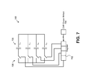
- FIG. 7 is a circuit diagram illustrating an adaptive resolution circuit including a successive approximation register (SAR) according to another embodiment.
- SAR successive approximation register
- FIG. 8 is a circuit diagram illustrating a capacitance-sensing circuit including an adaptive resolution circuit according to another embodiment.
- FIG. 9 is a flow diagram of a method of adaptive resolution for capacitance measurement according to an embodiment
- FIG. 10 is a block diagram illustrating one embodiment of an electronic system having a processing device including an adaptive resolution circuit.
- One apparatus includes an input node coupled to a capacitance sense pin coupled to an electrode of a sense array and a capacitance-sensing circuit coupled to the input node and including an integrator configured to measure a capacitance with a first resolution.
- An adaptive resolution circuit is coupled to the capacitance-sensing circuit and the input node and is configured to selectively modify an integration parameter to set the integrator to measure the capacitance with a second resolution.
- the integration parameter is an integration capacitance of the integrator.
- the integration parameter is an input resistance of the integrator.
- the integration parameter may be other programmable parameters of the integrator or the analog-to-digital converter.
- the term capacitor may refer to any combination of conductors and dielectrics that produce a capacitance between the conductors, as well as discrete components.
- a capacitance can created as an intersection between two electrodes.
- An intersection between the first electrode and second electrode is also called a sensor.
- An intersection between two sense elements may be understood as a location at which one sense electrode crosses over or overlaps another, while maintaining galvanic isolation from each other.
- a discrete capacitor may be used to produce a capacitance.
- FIG. 1 is a circuit diagram illustrating a capacitance-sensing circuit 100 according to one implementation.
- a transmit (TX) signal generator 101 generates a TX signal and applies the voltage on a TX electrode 102 (TX pin), and the integrator 110 measures the injected current through a RX electrode 104 (RX pin).
- the TX electrode 102 has a parasitic capacitance 105 (C PTX ) (a capacitance to ground) and the RX electrode 104 has a parasitic capacitance 107 (C PRX ).
- This current at an input node 116 is integrated by the integrator 110 , and the corresponding voltage that is measured provides insight into the change in capacitance 103 (C M ).
- the other input of integrator 110 is a voltage reference 118 (Vref).
- the capacitance 103 is a mutual capacitance between the TX electrode 102 and RX electrode 104 .
- the capacitance-sensing circuit 100 can be calibrated with a programmable current source 117 (IDAC) so that the voltage that is measured for no inputs is a known value.
- IDAC programmable current source 117
- This known value is typically set to be at a mid-scale of an analog-to-digital converter (ADC) 120 .
- ADC 120 measures anything other than mid-scale, then this new voltage is a result in a change in capacitance 103 , resulting from a touch on or near an intersection between the TX electrode 102 and the RX electrode 104 .
- the input current of the integrator 110 is balanced with the current source 117 , and the remaining current is integrated on the integrator capacitor 109 (C INT ) for a fixed period of time.
- the ADC 120 measures the voltage on the output of the integrator 110 and converts the voltage to a digital value 130 .
- the digital value 130 represents the capacitance sense result.
- the TX electrode 102 and RX electrode 104 represent one intersection of a touch surface, such as a touch surface of a touchscreen, touchpad, a panel, or the like.
- a resolution of capacitance-sensing circuit 100 is fixed.
- the actual resolution is related to the reference of the ADC 120 , the size of integrator capacitor 109 (C INT ), and the granularity of the programmable current source 117 (IDAC).
- Some or all of these parameters can be changed in firmware today, but once they are chosen, they are essentially fixed.
- the parameters are typically tuned for the type of touch object that is expected. This is usually a finger. However, the signal level for a passive stylus is much smaller than a typical finger signal. So, when a passive stylus is put on a touch surface, the change in voltage is not really noticed by the circuit 100 . Additionally, when there is noise on the panel, the capacitance-sensing circuit 100 can become saturated for a given range.
- the capacitance-to-digital conversion (CDC) range by the capacitance-sensing circuit 100 must be turned down to a smaller resolution.
- a normal touch saturates the input and the maximum voltage will always be read out.
- these two touch types cannot currently exist with the same circuit using the same integration time.
- the first approach creates a new scanning mechanism that the firmware must use for passive stylus.
- One such mechanism is called a balanced scan, in which all TX electrodes are driven at once. The effect of doing this is that the signal from a passive stylus is greatly enhanced.
- the sensitivity is so high that a normal touch once again will drown out the stylus. Therefore, Balanced Scan does not work with touches on the touch surface at the same time as a stylus.
- the other cost is a second scanning method, which consumes system resources like time and memory.
- the second approach scans the same intersection for longer if a stylus is expected to be present.
- the sensitivity can be increased by simply scanning longer, i.e., integrating over a longer period.
- the payoff is not good. Assuming white noise (best case), then it would take four times (4 ⁇ ) the scan time to get a two times (2 ⁇ ) signal-to-noise (SNR) gain. Therefore, the time penalty for this approach is very high.
- the firmware must know when to pay this penalty. If normal mutual capacitance scanning cannot detect a stylus in the first place, then the firmware can never move to a longer integration time. In effect, more resolution is achieved through a longer integration time, limited by a natural quantization of the system. These types of circuits take longer to scan and are not as accurate as the embodiments describe herein.
- the embodiments described below are directed to an adaptive resolution circuit for a capacitance-sensing circuit.
- the adaptive resolution circuit can be used to modify a resolution of the capacitance-sensing circuit.
- the adaptive resolution circuit measures an input of the capacitance-sensing circuit and determines an optimum resolution for the CDC conversion by the capacitance-sensing circuit. This would be like setting a multimeter device to measure mV or V depending on the intended input.
- the embodiments described herein can measure the effective input capacitance and determine the optimum measurement resolution, which in term creates the maximum possible sensitivity for the circuit for a given input.
- the adaptive resolution circuit when measuring a touch signal, can set the capacitance-sensing circuit to a first resolution (think setting the multimeter to 1V sensitivity), and when measuring a stylus signal, the adaptive resolution circuit can set the capacitance-sensing circuit to a second resolution (think setting the multimeter to 1 mV sensitivity).
- the capacitance-sensing circuit can use any type of capacitance measurement technique, such as CSD (CapSense Sigma Delta), CSA (CapSense Successive Approximation), or the like.
- CSD CapSense Sigma Delta
- CSA CapSense Successive Approximation
- FIG. 2 is a circuit diagram illustrating a capacitance-sensing circuit 200 including an adaptive resolution circuit 240 according to one embodiment.
- the capacitance-sensing circuit 200 includes an integrator 210 , a programmable current source 217 , two integrator capacitors 209 (C INT,stylus ) and 211 (C INT,touch ), a TX signal generator 201 , adaptive resolution circuit 240 , and ADC 220 .
- the integrator 210 measures current input at an input node 216 .
- a TX signal generator 201 generates a TX signal and applies the voltage on a TX electrode 202 (TX pin).
- the integrator 210 measures the injected current through a RX electrode 204 (RX pin).
- the TX electrode 202 has a parasitic capacitance 205 (C PTX ) (a capacitance to ground) and the RX electrode 204 has a parasitic capacitance 207 (C PRX ).
- the current at input node 216 is integrated by the integrator 210 , and the corresponding voltage that is measured provides insight into the change in mutual capacitance 203 (C M ) between the TX electrode 202 and the RX electrode 204 .
- the input node 216 is a node of an analog multiplexer bus (also referred to as AMUXBUSA).
- the other input of integrator 210 is a voltage reference 218 (Vref).
- the input current of the integrator 210 is balanced with the programmable current source 217 , and the remaining current is integrated on an integration capacitance for a fixed period of time.
- the integration capacitance is selectively modified by the adaptive resolution circuit 240 as described in more detail below.
- the ADC 220 measures the voltage on the output of the integrator 210 and converts the voltage to a digital value 230 .
- the digital value 230 represents the capacitance sense result.
- the TX electrode 202 and RX electrode 204 represent one intersection of a touch surface, such as a touch surface of a touchscreen, touchpad, a panel, or the like.
- the touch surface can have multiple intersections, such as multiple intersections between rows and columns or other electrode layouts.
- the resolution of capacitance-sensing circuit 200 is adaptive. As described above, the actual resolution is related to the reference of the ADC 220 , the size of integration capacitance (C INT ), and the granularity of the programmable current source 217 (IDAC). Instead of fixing these parameters in firmware as done conventional, the embodiments described herein can selectively modify the integration capacitance or can change a reference of the ADC 220 .
- the adaptive resolution circuit 240 can selectively modify the integration capacitance by selectively coupling an additional capacitor 211 (C INT,touch ) in parallel to an integrator capacitor 209 (C INT,stylus ).
- the reference of the ADC 220 , the sizes of the integrator capacitors and the granularity of the programmable current source 217 can be set in firmware, and the adaptive resolution circuit 240 can operate the capacitance-sensing circuit 200 at two different resolutions.
- the first resolution can be set so the capacitance-sensing circuit 200 can detect a stylus signal and the second resolution can be set so the capacitance-sensing circuit 200 can detect a finger signal.
- the signal level for a passive stylus is much smaller than a typical finger signal. So, when a passive stylus is put on a touch surface, the change in voltage can be readily noticed by the capacitance-sensing circuit 200 with the first resolution.
- the capacitance-sensing circuit 200 can use the second resolution to detect the change in voltage by a finger.
- the capacitance-to-digital conversion (CDC) range by the capacitance-sensing circuit 200 can be adaptively tuned down to a smaller resolution than when measuring a finger.
- the capacitance-sensing circuit 200 with the adaptive resolution circuit 240 allows these two touch types to be measured by the same capacitance-sensing circuit 200 using the same integration time.
- the adaptive resolution circuit 240 can selectively modify the integration capacitance, the programmable current source 217 (IDAC) can be calibrated so that the voltage that is measured for no inputs is a known value. This known value is typically set to be at a mid-scale of the ADC 220 for stylus detection. When the ADC 220 measures anything other than mid-scale, then this new voltage is a result in a change in mutual capacitance 203 , resulting from a touch by a stylus on or near an intersection between the TX electrode 202 and the RX electrode 204 . The selective coupling of the additional capacitor 211 changes the gain of the integrator 210 . In other embodiments, instead of selectively modifying the integration capacitance, the adaptive resolution circuit 240 can modify a voltage reference of the ADC 220 as described with respect to FIG. 8 .
- the adaptive resolution circuit 240 is coupled to the input node 216 and an output of the integrator 210 .
- the adaptive resolution circuit 240 is configured to selectively modify an integration capacitance of the integrator 210 to set the integrator to measure the mutual capacitance 203 with either a first resolution or a second resolution.
- the adaptive resolution circuit 240 includes an additional capacitor 211 (C INT,touch ), a comparator 212 , a switch 213 and a register 214 .
- the comparator 212 is coupled to the output of the integrator 210 and the switch 213 is coupled to an output of the comparator 212 .
- the comparator 212 is configured to selectively switch the capacitor 211 in parallel to the integrator capacitor 209 to modify the integration capacitance of the integrator 210 for the second resolution.
- the adaptive resolution circuit 240 also includes a control circuit that includes a register 214 .
- the register 214 can track switches between the transitions in resolution for the firmware.
- the control circuit can be more complex to determine when to switch in one or more additional capacitors, as described herein.
- the register 214 is a shift register, as illustrated in FIG. 6 , which is used to set the variable integration capacitance using one or more capacitors based on the output of the comparator 212 .
- the register 214 is a register, as illustrated in FIG. 7 , which is used to set the variable integration capacitance using one or more capacitors based on the output of the comparator 212 .
- the adaptive resolution circuit 240 may include multiple switches coupled to a bank of capacitors, and the comparator 212 and register 214 can be used to select different combinations of the bank of capacitors to selectively modify the integration capacitance of the integrator 210 . That is the adaptive resolution circuit 240 can selectively couple one or more of the bank of capacitors to the input node 216 to modify the integration capacitance of the integrator 210 to multiple resolutions other than the first resolution.
- the total integration capacitance is the capacitance of the capacitor 209 and the selected combination of the bank of capacitors.
- the programmable current source 217 is a single programmable current source that can be configured to operate as a current source or a current sink.
- the programmable current source 217 can be configured as a current source to the input node 216 during a portion of a TX cycle of the TX signal and as a current sink to the input node 216 during another portion of the TX cycle.
- the programmable current source 217 includes two separate programmable current sources, one programmable current source is configured as a current source and the other programmable current source is configured as a current sink.
- the input node 216 is coupled to a capacitance sense pin, which is coupled to a RX electrode 204 of a sense array.
- the TX signal generation circuit 201 generates a TX signal to drive a TX electrode 202 of the sense array.
- a mutual capacitance between the first electrode and the second electrode is represented as capacitor 203 (C M ).
- the adaptive resolution circuit 240 deactivates the switch 213 , and the RX signal on the input node 216 is integrated by the integrator 210 with the integrator capacitor 209 .
- the ADC 220 converts the integrated signal into a first digital value 230 .
- the first digital value 230 represents a mutual capacitance between the RX electrode 204 and the second electrode 206 , C M 203 at the first resolution.
- the digital value 230 can be further processed by a processing device (e.g., 1010 of FIG. 10 ) or a host (e.g., 1050 of FIG. 10 ).
- the adaptive resolution circuit 240 measures the output of the integrator 210 with the comparator 212 . When the output signal of the integrator 210 is above a comparator threshold, the adaptive resolution circuit 240 can activate the switch 213 to couple the additional capacitor 211 (C INT,touch ) in parallel to the integrator capacitor 209 .
- the ADC 220 converts the integrated signal into a second digital value 230 .
- the digital value 230 represents a mutual capacitance between the RX electrode 204 and the second electrode 206 , C M 203 at the second resolution.
- additional capacitors can be switched into parallel (or in other configurations) to selectively modify the integration capacitance to selectively modify the resolutions of the capacitance-sensing circuit 200 .
- a processing device includes an integrator, a multiplexer bus coupled to an input of the integrator.
- the multiplexer is configured to selectively couple the input node to an electrode of a sense array.
- An adaptive resolution circuit is coupled to the input node and the output of the integrator.
- the adaptive resolution circuit is configured to selectively modify an integration capacitance of the integrator to set the integrator to measure a capacitance associated with the electrode with one of multiple programmable resolutions.
- the processing device includes an ADC coupled to an output of the integrator to convert an integrated capacitance to a digital value.
- the adaptive resolution circuit includes an adaptive capacitance circuit to provide a variable capacitance, a comparator coupled to the output of the integrator, and a control circuit coupled to an output of the comparator.
- the control circuit is configured to set the variable capacitance of the adaptive capacitance circuit to selectively modify the integration capacitance of the integrator.
- the capacitance-sensing circuit 200 is configured to sense a small passive stylus at the same time as a normal finger touch.
- the level of sensitivity between these two touch input domains may be twenty-five times (25 ⁇ ) or greater.
- a passive stylus may have a signal of 10 and a finger may have a signal of 250.
- the larger finger signal can easily swamp out the small stylus signal, which means the stylus cannot be accurately reported or even detected by a conventional touch screen controller.
- touch screen controllers that utilize the capacitance-sensing circuit 200 can detect both signals.
- the capacitance-sensing circuit 200 uses two integration capacitors and the adaptive resolution circuit 240 for detecting the measured signal modifying a resolution of the capacitance-sensing circuit 200 based on the measured signal.
- the adaptive resolution circuit 240 can be a signal detection circuit to detect the signal and control circuitry to modify either the integration capacitance or the reference of the ADC 220 as described herein.
- the smaller integration capacitor is more sensitive than the larger integration capacitor, so it can be connected at all times in one implementation. If the detection circuit notices that the smaller integration capacitor has become saturated, then the detection circuit connects the larger capacitor and issue a re-measure command to the firmware. For example, this can be done by coupling the output of the comparator 212 to a register 214 that can be read by the firmware. Therefore, the finger input that saturated the stylus capacitor, can be sensed when the finger cap is connected.
- the adaptive resolution circuit shown in FIG. 2 can further be extrapolated to a bank of capacitors that can be adaptively configured to create a larger and larger integration capacitance for more levels of sensitivity than just two as done in FIG. 2 .
- a more generalized approach to varying the integration capacitance is shown in FIG. 3 .
- a secondary control circuit e.g., 314 of FIG. 3
- the adaptive resolution circuit can be tuned to maximize the sensitivity of the capacitance-sensing circuit.
- the input can be measured and the capacitance-sensing circuit can adaptively adjust the integration capacitance to maximize its sensitivity.
- the control circuit can be as simple as the circuit shown in FIG. 2 , where the integration capacitor is incrementally increased until it is no longer saturated from the input.
- a more intelligent detection and control circuit could also be used to converge to the appropriate capacitance value faster. For instance, a successive approximation circuit could be used to perform a binary search for the optimum capacitance, which would converge to a result much faster than the incremental approach.
- Another approach may be to use the largest capacitance possible (to guarantee no saturation) and use the ADC output of the first measurement to determine the necessary size of the integration capacitance for the next scan.
- the integrator 210 is illustrated and described as an active integrator or operational amplifier integrator. In other embodiments, the integrator 210 may be a passive integrator or other device to perform integration. Also, in other embodiments, instead of selectively modifying the integration capacitance of the integrator, other integration parameters may be selectively modified.
- the integration parameter may be a capacitance, an input resistance or impedance, a voltage reference, or the like.
- the input resistance of the integrator 210 can be selectively modified to set the integrator to measure at one or more different resolutions.
- a voltage reference of the ADC 220 can be selectively modified convert the measured capacitance at one or more different resolutions.
- FIG. 3 is a circuit diagram illustrating a capacitance-sensing circuit 300 including an adaptive resolution circuit 340 according to another embodiment.
- the capacitance-sensing circuit 300 is similar to the capacitance-sensing circuit 200 as noted by similar reference numbers, except the capacitance-sensing circuit 300 includes the adaptive resolution circuit 340 .
- the adaptive resolution circuit 340 includes an adaptive capacitance circuit 311 , a comparator 312 , and a control circuit 314 .
- the adaptive capacitance circuit 311 can be used to provide an adaptive integration capacitance for the integrator 210 .
- the adaptive resolution circuit 340 can set the adaptive capacitance circuit 311 to automatically set the resolution (i.e., sensitivity) of the capacitance-sensing circuit 300 .
- the adaptive capacitance circuit 311 can be implemented using various circuit elements and various circuit configurations to create varying capacitance levels. One implementation is illustrated in FIG. 5 . In another embodiment, the adaptive resolution circuit 340 includes an impedance converter circuit instead of the adaptive capacitance circuit 311 . One implementation of the impedance converter circuit is illustrated in FIG. 4 .
- the adaptive capacitance circuit 311 can be configured to provide a variable capacitance (i.e., set to have different capacitance values).
- the adaptive capacitance circuit 311 is configured to operate as an integrator capacitor of the integrator 210 .
- the comparator 312 is coupled to the output of the integrator 210 and measures the integrated signal.
- the comparator 312 is configured to selectively set the variable capacitance of the adaptive capacitance circuit 311 to modify the integration capacitance of the integrator 210 for the second resolution (variable resolution).
- the control circuit 314 is coupled to the output of the comparator 312 and can be used to determine the capacitance level needed for the adaptive capacitance circuit 311 .
- the control circuit 314 sets the adaptive capacitance circuit 311 based on the output of the comparator 312 .
- the control circuit 314 includes a shift register to set the adaptive capacitance circuit 311 to an appropriate value for a given resolution.
- the control circuit 314 includes a register to set the adaptive capacitance circuit 311 to an appropriate value for a given resolution. Additional details of the control circuit 314 are described below with respect to FIGS. 6 and 7 . It should be noted that the depicted embodiment, shows the adaptive capacitance circuit 311 as the integrator capacitor of the integrator 210 . However, in other embodiments, the adaptive capacitance circuit 311 can be used in connection with an integrator capacitor (e.g., 209 ) of the integrator 210 .
- the impedance converter circuit (substituted for the adaptive capacitance circuit 311 ) can be configured to provide a variable impedance (i.e., set to have different impedance values).
- the impedance converter circuit is configured to operate as an integrator capacitor of the integrator 210 .
- the comparator 312 is coupled to the output of the integrator 210 and measures the integrated signal.
- the comparator 312 and the control circuit 314 are configured to selectively set the variable impedance of impedance converter circuit to modify the integration capacitance of the integrator 210 for the second resolution (variable resolution). It should be noted that the impedance converter circuit can be used in connection with or without an integrator capacitor of the integrator 210 .
- Embodiments described herein such as those illustrated in FIG. 2 and FIG. 3 that provide adaptive sensitivity of the sensing circuits provide improved systems than conventional systems.
- the embodiments described herein provide a hardware approach to simultaneously measure a passive stylus and a normal touch. Additionally, the embodiments described can provide good noise immunity to high noise inputs such as charger noise by preventing the integration capacitor from saturating when high noise is injected into the system. Solutions today must use longer integration times and other firmware based techniques to increase sensitivity. These techniques have diminishing returns as well as other negative effects such as a reduction in scan time and report rate as describe herein.
- the embodiments described herein can be used to measure capacitive inputs of varying size without a manual tuning intervention. FIG.
- FIG. 2 shows a specific implementation of measuring two discrete capacitive input ranges. Further extending the capacitance bank of FIG. 2 would allow additional inputs ranges. Each new feedback capacitor size would indicate a new capacitance range to measure.
- FIG. 3 shows a generalized implementation of FIG. 2 as a proposal to use an adjustable capacitor instead of several discrete capacitors.
- FIG. 5 shows one possible implementation for creating such a capacitor for the adaptive capacitance circuit in FIG. 3 . Any gains in sensitivity can be stored in firmware so the ADC values can be properly interpreted.
- One improvement may be a higher sensitivity for small capacitive inputs without affecting the sensitivity of larger capacitance inputs. This manifests itself in two different ways. Firstly, if the panel hardware is tuned for small inputs, than the larger inputs produce false positives for smaller inputs at the periphery of the touch. In other words, the edges of a large touch have small signal levels close enough signify to the firmware that a small touch is present (such as a passive stylus). Secondly, if the panel is tuned for larger touches, than the firmware will also not detect the smaller touch objects.
- the embodiments described herein can provide two improvements here; the embodiments can eliminate false positives (reported touches that are not there) and false negatives (un-reported touches that are there). These problems are especially relevant when the firmware must support a large range of expected touch inputs.
- FIG. 1 shows the previous method, which uses a static integration capacitor to measure input capacitance. Although this cap can be changed through firmware for some touch screen solutions, once chosen the value is static for any measurements on the touch screen. Additionally, because of silicon area, the number of selections is often limited, which means the range of the measurement is also limited.
- FIGS. 2 and 3 show improvements to the existing circuit which measure the capacitive input and decide the necessary level of sensitivity.
- the capacitance-sensing circuit includes the following: 1) adaptive integration capacitance: either through a capacitance bank ( FIG. 2 ), impedance converter ( FIG. 3 ), or some other method; 2) a circuit to measure integration capacitance saturation. In FIGS. 2 and 3 this is the comparator (CMP); and 3) a mechanism or method to control the circuit in 1) by the outputs of 2). This could be something like a circular shift register, such as illustrated in FIG. 6 , as an input to a MUX or some other hardware solution.
- the capacitance-sensing circuit can be implemented in an analog front end (AFE) to a touchscreen controller.
- AFE analog front end
- the capacitance-sensing circuit with variable resolution can rely on the necessary software components to analyze the analog result and produce useful information. For example, firmware can be used to process the capacitive heat map and produce any known touch locations. This software could also be implemented on a host processor, which implies that only a digital communication interface would be needed in addition to the analog front end. In other embodiments, other capacitance measurement circuits can be used. If the input source is current, then hardware analog integration may be used to resolve the input capacitance and the sensitivity of the integration is proportional to impedance (typically capacitor). This size of this impedance dictates the level of sensitivity. So, the measurement circuit can be configured to sense the level of the input and change this impedance to match the necessary level of sensitivity.
- impedance typically capacitor
- FIG. 4 is a circuit diagram illustrating a generalized impedance converter circuit 400 according to one embodiment.
- This type of circuit uses two operational amplifiers 420 , 430 and five circuit elements 410 .
- These circuit elements 410 can be capacitors or resistors.
- the generalized impedance converter circuit 400 can produce a varying type of impedance 406 .
- the generalized impedance converter circuit 400 can look like a resistor, capacitor, inductor, or even negative resistor.
- This type of circuit is used in filtering applications or in integrated circuit (IC) designs that cannot afford to use a real inductor because of the physical size.
- the transfer function of this circuit is shown in Equation 1.
- the impedance converter circuit 400 includes multiple circuit elements 410 coupled in series between an input terminal 402 and an output terminal 404 .
- a first operational amplifier 420 includes inputs coupled between the input terminal 402 and a first intervening node 408 and an output coupled to a second intervening node 412 .
- a second operational amplifier 430 includes inputs coupled between the first intervening node 408 and a third intervening node 414 and an output coupled to a fourth intervening node 416 .
- FIG. 5 is a circuit diagram illustrating an adaptive capacitance circuit 500 according to one embodiment.
- the type of circuit of FIG. 4 can be configured as a variable capacitance circuit.
- the adaptive capacitance circuit 500 uses two operational amplifiers 520 , 530 and a capacitive element 512 and four resistive elements 510 . Instead of providing a varying type of impedance 406 , the adaptive capacitance circuit 500 provides a variable type of capacitance 506 .
- the adaptive capacitance circuit 500 is a general impedance converter configured to provide a variable capacitance. For example, if one or more of the resistors are variable, then the total capacitance of the circuit is also variable. The variable capacitance of this circuit is shown in Equation 2.
- the adaptive capacitance circuit 500 includes multiple resistive elements 510 coupled in series between an input terminal 502 and an output terminal 504 and a capacitive element couple between two intervening resistive elements.
- a first operational amplifier 520 includes inputs coupled between the input terminal 502 and a first intervening node 508 and an output coupled to a second intervening node 512 .
- a second operational amplifier 530 includes inputs coupled between the first intervening node 508 and a third intervening node 514 and an output coupled to a fourth intervening node 516 .
- FIG. 6 is a circuit diagram illustrating an adaptive resolution circuit 600 including a shift register 602 according to one embodiment.
- the adaptive resolution circuit 600 implements a straight linear adder to set the variable capacitance.
- a first capacitor of a bank of capacitors 606 is always set for a default integration capacitance. If the output of the comparator, represented by CMP output bitfield 604 , is HIGH then the output is placed in the leftmost field of the shift register 602 , which adds in another capacitor (lower capacitor) of the capacitor bank.
- a first switch can be controlled by the leftmost field of the shift register 602 to couple the additional capacitor in parallel to the first capacitor.
- the shift register 602 shifts the elements to the left, which turns on the middle capacitor and the lower capacitor of the capacitor bank 606 . If the CMP output bitfield 604 is low, the shift register 602 does not add in a capacitor and knows it is at its optimal resolution. It should be noted that the adaptive resolution circuit 600 is illustrated and described using four capacitors in the capacitor bank 606 and three elements in the shift register 602 . In other embodiments, other number of capacitors in the capacitor bank 606 and elements in the shift register 602 can be used.
- a normal register can be used where a pointer of the comparator is shifted along a length of the register as illustrated in FIG. 7 .
- FIG. 7 is a circuit diagram illustrating an adaptive resolution circuit 700 including a successive approximation register (SAR) 702 according to another embodiment.
- the adaptive resolution circuit 700 implements a SAR approach to set the variable capacitance.
- a first capacitor of a bank of capacitors 706 is always set for a default integration capacitance.
- a pointer of the comparator can be shifted along the length of the register 702 and an output of the comparator, represented as CMP output bitfield 704 , is AND'ed with a bit of the element of the register 702 .
- one capacitor of the capacitor bank 706 that corresponds to the element can be set or not based on AND operation of the comparator output 704 and the bit of the element.
- the capacitor is set (or selected). That is the corresponding switch is activated to couple the capacitor in parallel to the first capacitor when set. If the CMP output bitfield 704 is ‘0’, then the capacitor should not be set.
- the highest possible C value is 15, and the smallest is 1. Any number from 1 to 15 can be chosen by adding at least some of the 1 ⁇ , 2 ⁇ , 4 ⁇ and 8 ⁇ capacitors. So, the SAR logic determines out what value to choose between 1 and 15 in exactly 3 tests. Firstly, C1X is selected. Next, C8X is set. If the result is saturated, then 8X isn't good enough and it should remain being SET. If the result isn't saturated, then the value of 8X is too high so it should not be SET. Hence, the setting of the bit is a logical AND with the result. The C4X, C2X, and C1X are tested in the same way. At the end, the optimum value would be selected.
- the desired value is C13X
- the C8X is set and because C13X is needed, C8X will be saturated and the CMP will be high, so C8X is left selected.
- FIG. 8 shows a generalized approach to adaptively adjusting the sensitivity (resolution) by selectively modifying the ADC reference.
- FIG. 8 is a circuit diagram illustrating a capacitance-sensing circuit 800 including an adaptive resolution circuit according to another embodiment.
- the capacitance-sensing circuit 800 is similar to the capacitance-sensing circuit 200 as noted by similar reference numbers, except the capacitance-sensing circuit 800 includes the adaptive resolution circuit 840 .
- the adaptive resolution circuit 840 includes an adaptive ADC voltage reference (Vref) circuit 811 coupled to an output of a comparator 812 .
- the adaptive resolution circuit 840 also includes a control circuit 814 , which is similar to the control circuit 314 as described above. Unlike the adaptive capacitance circuit 311 of FIG.
- the adaptive ADC Vref circuit 811 is configured to selectively modify a voltage reference for the ADC 220 to convert the measured capacitance with the second resolution (variable resolution).
- the adaptive resolution circuit 840 can set the voltage reference (ADC reference) to automatically set the resolution (i.e., sensitivity) of the ADC 220 .
- ADC reference the voltage reference
- the comparator 812 measure the integrated signal output from the integrator 210 to determine a resolution of the ADC 220 and can adjust the voltage reference accordingly to set the resolution.
- the control circuit 814 is coupled to the output of the comparator 812 and can be used to determine the voltage reference needed for the ADC 220 .
- the control circuit 814 sets the adaptive ADC Vref circuit 811 based on the output of the comparator 812 .
- the control circuit 814 includes a shift register to set the adaptive ADC Vref circuit 811 to an appropriate value for a given resolution.
- the control circuit 814 includes a register to set the adaptive ADC Vref circuit 811 to an appropriate value for a given resolution.
- the adaptive ADC Vref circuit 811 can modify an output voltage to selectively modify the ADC reference for the ADC 220 . Modifying an output voltage can be achieved through a simple resistor based voltage divider, or through an active circuit using an operational amplifier as a buffer with gain.
- the embodiments described herein can be implemented in a touchscreen controller used in a touchscreen device, such as a point of sale terminals, trackpads, or any other touch input device.
- the embodiments described herein can also be used in other touch devices, such as a computer trackpad, or other types of touch input devices.
- passive stylus is rapidly becoming a standard market feature.
- conventional solutions do not permit detection of the stylus with touches on the same screen. This may mean that palm and grip rejection are not possible in these solutions.
- the embodiments described herein may be used in connection with features, such as palm and grip rejection features.
- the embodiments described herein may also provide a noise abatement procedure for normal touches, which may be an improvement over the conventional data filtering methods.
- FIG. 9 is a flow diagram of a method 900 of adaptive resolution for capacitance measurement according to an embodiment.
- the method 900 may be performed by processing logic that may comprise hardware (circuitry, dedicated logic, etc.), software (such as is run on a general purpose computing system or a dedicated machine), firmware (embedded software), or any combination thereof.
- the capacitance-sensing circuit 200 of FIG. 2 or capacitance-sensing circuit 300 of FIG. 3 performs the method 900 .
- the processing device 1010 performs the method 900 .
- the adaptive resolution circuit 1020 performs the method 900 .
- other components of the electronic system 1000 perform some or all of the operations of method 900 .
- the method 900 begins with processing logic receiving at an input node of a capacitance-sensing circuit a receive (RX) signal on a capacitance sense pin coupled to an electrode of a sense array (block 902 ).
- the processing logic integrates the RX signal by an integrator comprising an integrator capacitor with a first resolution of the capacitance-sensing circuit (block 904 ).
- the processing logic determines if a new resolution is needed (e.g., integration capacitance is saturated or near saturated) (block 906 ). If no new resolution is needed, the processing logic returns to block 902 .
- the processing logic selectively couples an additional capacitance to the integrator capacitor to modify the integrator to integrate with a second resolution (block 908 ).
- one or more additional capacitors can be coupled to the integrator capacitor to vary the integration capacitance to one or more different levels.
- the processing logic integrates the RX signal by the integrator with the second resolution. The processing logic returns to block 906 to determine if a new resolution is needed.
- the processing logic compares an output of the integrator with a comparator and selectively couples a second capacitor in parallel to the integrator capacitor to modify the integration capacitance for the second resolution based on the output of the comparator.
- the processing logic compares an output of the integrator with a comparator and selectively sets an impedance of an impedance converter circuit coupled between the input node and the output of the integrator to modify the integration capacitance of the integrator for the second resolution.
- the processing logic compares an output of the integrator with a comparator and selectively sets a variable capacitance of an adaptive capacitance circuit coupled between the input node and the output of the integrator to modify the integration capacitance of the integrator for the second resolution.
- the processing logic receives an output of the comparator and controls the variable capacitance of the adaptive capacitance circuit using at least one of a register or a shift register as described herein.
- the processing logic may perform other operations as described above with respect to FIGS. 2-8 .
- the capacitive touch screen controller is the TrueTouch® capacitive touchscreen controllers, such as the CY8CTMA3xx family of TrueTouch® Multi-Touch All-Points touchscreen controllers, developed by Cypress Semiconductor Corporation of San Jose, Calif.
- the TrueTouch® capacitive touchscreen controllers sensing technology to resolve touch locations of multiple fingers and a stylus on the touch-screens, supports leading operating systems, and is optimized for low-power multi-touch gesture and all-point touchscreen functionality.
- the touch position calculation features may be implemented in other touchscreen controllers, or other touch controllers of touch-sensing devices.
- the touch position calculation features may be implemented with other touch filtering algorithms as would be appreciated by one of ordinary skill in the art having the benefit of this disclosure.
- FIG. 10 is a block diagram illustrating one embodiment of an electronic system 1000 having a processing device 1010 including adaptive resolution circuit 1020 . Details regarding the adaptive resolution circuit 1020 are described in more detail with respect to FIGS. 2-8 .
- the processing device 1010 is configured to detect one or more touches on a touch-sensing device, such as the capacitive sense array 1025 .
- the processing device can detect conductive objects, such as touch objects 1040 (fingers or passive styluses, an active stylus 1030 , or any combination thereof.
- the capacitance-sensing circuit 1001 can measure touch data on the capacitive sense array 1025 .
- the touch data may be represented as multiple cells, each cell representing an intersection of sense elements (e.g., electrodes) of the capacitive sense array 1025 .
- the touch data is a 2D capacitive image of the capacitive sense array 1025 .
- the capacitance-sensing circuit 1001 measures mutual capacitance of the touch-sensing device (e.g., capacitive sense array 1025 )
- the capacitance-sensing circuit 1001 obtains a 2D capacitive image of the touch-sensing device and processes the data for peaks and positional information.
- the processing device 1010 is a microcontroller that obtains a capacitance touch signal data set, such as from a sense array, and finger detection firmware executing on the microcontroller identifies data set areas that indicate touches, detects and processes peaks, calculates the coordinates, or any combination therefore.
- the firmware identifies the peaks using the embodiments described herein.
- the firmware can calculate a precise coordinate for the resulting peaks.
- the firmware can calculate the precise coordinates for the resulting peaks using a centroid algorithm, which calculates a centroid of the touch, the centroid being a center of mass of the touch.
- the centroid may be an X/Y coordinate of the touch.
- other coordinate interpolation algorithms may be used to determine the coordinates of the resulting peaks.
- the microcontroller can report the precise coordinates to a host processor, as well as other information.
- Electronic system 1000 includes processing device 1010 , capacitive sense array 1025 , stylus 1030 , host processor 1050 , embedded controller 1060 , and non-capacitive sense elements 1070 .
- the capacitive sense elements are electrodes of conductive material, such as copper.
- the sense elements may also be part of an ITO panel.
- the capacitive sense elements can be configurable to allow the capacitive-sensing circuit 1001 to measure self-capacitance, mutual capacitance, or any combination thereof.
- the electronic system 1000 includes the capacitive sense array 1025 coupled to the processing device 1010 via bus 1022 .
- the capacitive sense array 1025 may include a multi-dimension capacitive sense array.
- the multi-dimension sense array includes multiple sense elements, organized as rows and columns.
- the capacitive sense array 1025 operates as an all-points-addressable (“APA”) mutual capacitive sense array.
- the capacitive sense array 1025 operates as a coupled-charge receiver.
- the capacitive sense array 1025 is non-transparent capacitive sense array (e.g., PC touchpad).
- the capacitive sense array 1025 may be disposed to have a flat surface profile. Alternatively, the capacitive sense array 1025 may have non-flat surface profiles. Alternatively, other configurations of capacitive sense arrays may be used.
- the capacitive sense array 1025 may have a hexagon arrangement, or the like, as would be appreciated by one of ordinary skill in the art having the benefit of this disclosure.
- the capacitive sense array 1025 may be included in an ITO panel or a touch screen panel.
- the processing device 1010 is configurable to detect a presence of the touch object 1040 , a presence of a stylus 1030 on the capacitive sense array 1025 , or any combination thereof.
- the processing device 1010 may detect and track the stylus 1030 and the touch object 1040 individually on the capacitive sense array 1025 .
- the processing device 1010 can detect and track both the stylus 1030 and touch object 1040 concurrently on the capacitive sense array 1025 .
- the active stylus 1030 is configurable to operate as the timing “master,” and the processing device 1010 adjusts the timing of the capacitive sense array 1025 to match that of the active stylus 1030 when the active stylus 1030 is in use.
- the capacitive sense array 1025 capacitively couples with the active stylus 1030 , as opposed to conventional inductive stylus applications. It should also be noted that the same assembly used for the capacitive sense array 1025 , which is configurable to detect touch objects 1040 , is also used to detect and track a stylus 1030 without an additional PCB layer for inductively tracking the active stylus 1030 .
- the processing device 1010 includes analog and/or digital general purpose input/output (“GPIO”) ports 1007 .
- GPIO ports 1007 may be programmable.
- GPIO ports 1007 may be coupled to a Programmable Interconnect and Logic (“PIL”), which acts as an interconnect between GPIO ports 1007 and a digital block array of the processing device 1010 (not shown).
- PIL Programmable Interconnect and Logic
- the digital block array may be configurable to implement a variety of digital logic circuits (e.g., DACs, digital filters, or digital control systems) using, in one embodiment, configurable user modules (“UMs”).
- UMs configurable user modules
- the digital block array may be coupled to a system bus.
- Processing device 1010 may also include memory, such as random access memory (“RAM”) 1005 and program flash 1004 .
- RAM random access memory
- program flash 1004 program flash
- RAM 1005 may be static RAM (“SRAM”), and program flash 1004 may be a non-volatile storage, which may be used to store firmware (e.g., control algorithms executable by processing core 1002 to implement operations described herein).
- Processing device 1010 may also include a memory controller unit (“MCU”) 1003 coupled to memory and the processing core 1002 .
- the processing core 1002 is a processing element configured to execute instructions or perform operations.
- the processing device 1010 may include other processing elements as would be appreciated by one of ordinary skill in the art having the benefit of this disclosure.
- the memory may be internal to the processing device or external to it. In the case of the memory being internal, the memory may be coupled to a processing element, such as the processing core 1002 . In the case of the memory being external to the processing device, the processing device is coupled to the other device in which the memory resides as would be appreciated by one of ordinary skill in the art having the benefit of this disclosure.
- the processing device 1010 may also include an analog block array (not shown).
- the analog block array is also coupled to the system bus.
- Analog block array may also be configurable to implement a variety of analog circuits (e.g., ADCs or analog filters) using, in one embodiment, configurable UMs.
- the analog block array may also be coupled to the GPIO 1007 .
- capacitance-sensing circuit 1001 may be integrated into processing device 1010 .
- Capacitance-sensing circuit 1001 may include analog I/O for coupling to an external component, such as touch-sensor pad (not shown), capacitive sense array 1025 , touch-sensor slider (not shown), touch-sensor buttons (not shown), and/or other devices.
- the capacitance-sensing circuit 1001 may be configurable to measure capacitance using mutual-capacitance sensing techniques, self-capacitance sensing technique, charge coupling techniques or the like.
- capacitance-sensing circuit 1001 operates using a charge accumulation circuit, a capacitance modulation circuit, or other capacitance sensing methods known by those skilled in the art.
- the capacitance-sensing circuit 1001 is of the Cypress TMA-3xx, TMA-4xx, or TMA-xx families of touch screen controllers. Alternatively, other capacitance-sensing circuits may be used.
- the mutual capacitive sense arrays, or touch screens, as described herein, may include a transparent, conductive sense array disposed on, in, or under either a visual display itself (e.g. LCD monitor), or a transparent substrate in front of the display.
- the TX and RX electrodes are configured in rows and columns, respectively. It should be noted that the rows and columns of electrodes can be configured as TX or RX electrodes by the capacitance-sensing circuit 1001 in any chosen combination.
- the TX and RX electrodes of the sense array 1025 are configurable to operate as a TX and RX electrodes of a mutual capacitive sense array in a first mode to detect touch objects, and to operate as electrodes of a coupled-charge receiver in a second mode to detect a stylus on the same electrodes of the sense array.
- the stylus which generates a stylus TX signal when activated, is used to couple charge to the capacitive sense array, instead of measuring a mutual capacitance at an intersection of a RX electrode and a TX electrode (a sense element) as done during mutual-capacitance sensing.
- An intersection between two sense elements may be understood as a location at which one sense electrode crosses over or overlaps another, while maintaining galvanic isolation from each other.
- the capacitance-sensing circuit 1001 does not use mutual-capacitance or self-capacitance sensing to measure capacitances of the sense elements when performing a stylus sensing. Rather, the capacitance-sensing circuit 1001 measures a charge that is capacitively coupled between the sense array 1025 and the stylus as described herein.
- the capacitance associated with the intersection between a TX electrode and an RX electrode can be sensed by selecting every available combination of TX electrode and RX electrode.
- the location of the finger on the capacitive sense array 1025 can be determined by identifying the RX electrode having a decreased coupling capacitance between the RX electrode and the TX electrode to which the TX signal was applied at the time the decreased capacitance was measured on the RX electrode. Therefore, by sequentially determining the capacitances associated with the intersection of electrodes, the locations of one or more inputs can be determined.
- the process can calibrate the sense elements (intersections of RX and TX electrodes) by determining baselines for the sense elements. It should also be noted that interpolation may be used to detect finger position at better resolutions than the row/column pitch as would be appreciated by one of ordinary skill in the art having the benefit of this disclosure. In addition, various types of coordinate interpolation algorithms may be used to detect the center of the touch as would be appreciated by one of ordinary skill in the art having the benefit of this disclosure.
- the capacitance-sensing circuit 1001 includes the adaptive resolution circuit 1020 . Additional details of the adaptive resolution circuit 1020 are described above with respect to FIGS. 2-8 .
- the electronic system 1000 may also include non-capacitive sense elements 1070 coupled to the processing device 1010 via bus 1071 and GPIO port 1007 .
- the non-capacitive sense elements 1070 may include buttons, light emitting diodes (“LEDs”), and other user interface devices, such as a mouse, a keyboard, or other functional keys that do not use capacitance sensing.
- buses 1022 , and 1071 are embodied in a single bus. Alternatively, these buses may be configured into any combination of one or more separate buses.
- Processing device 1010 may include internal oscillator/clocks 1006 and communication block (“COM”) 1008 .
- the processing device 1010 includes a spread spectrum clock (not shown).
- the oscillator/clocks block 1006 provides clock signals to one or more of the components of processing device 1010 .
- Communication block 1008 may be used to communicate with an external component, such as a host processor 1050 , via host interface (“I/F”) line 1051 .
- processing device 1010 may also be coupled to embedded controller 1060 to communicate with the external components, such as host processor 1050 .
- the processing device 1010 is configurable to communicate with the embedded controller 1060 or the host processor 1050 to send and/or receive data.
- Processing device 1010 may reside on a common carrier substrate such as, for example, an integrated circuit (“IC”) die substrate, a multi-chip module substrate, or the like. Alternatively, the components of processing device 1010 may be one or more separate integrated circuits and/or discrete components. In one exemplary embodiment, processing device 1010 is the Programmable System on a Chip (PSoC®) processing device, developed by Cypress Semiconductor Corporation, San Jose, Calif. Alternatively, processing device 1010 may be one or more other processing devices known by those of ordinary skill in the art, such as a microprocessor or central processing unit, a controller, special-purpose processor, digital signal processor (“DSP”), an application specific integrated circuit (“ASIC”), a field programmable gate array (“FPGA”), or the like.
- PSoC® Programmable System on a Chip
- DSP digital signal processor
- ASIC application specific integrated circuit
- FPGA field programmable gate array
- processing device 1010 may be done in the host.
- Capacitance-sensing circuit 1001 may be integrated into the IC of the processing device 1010 , or alternatively, in a separate IC. Alternatively, descriptions of capacitance-sensing circuit 1001 may be generated and compiled for incorporation into other integrated circuits.
- behavioral level code describing the capacitance-sensing circuit 1001 , or portions thereof, may be generated using a hardware descriptive language, such as VHDL or Verilog, and stored to a machine-accessible medium (e.g., CD-ROM, hard disk, floppy disk, etc.).
- the behavioral level code can be compiled into register transfer level (“RTL”) code, a netlist, or even a circuit layout and stored to a machine-accessible medium.
- the behavioral level code, the RTL code, the netlist, and the circuit layout may represent various levels of abstraction to describe capacitance-sensing circuit 1001 .
- electronic system 1000 may include all the components described above. Alternatively, electronic system 1000 may include some of the components described above.
- the electronic system 1000 is used in a tablet computer.
- the electronic device may be used in other applications, such as a notebook computer, a mobile handset, a personal data assistant (“PDA”), a keyboard, a television, a remote control, a monitor, a handheld multi-media device, a handheld media (audio and/or video) player, a handheld gaming device, a signature input device for point of sale transactions, an eBook reader, global position system (“GPS”) or a control panel.
- PDA personal data assistant
- the embodiments described herein are not limited to touch screens or touch-sensor pads for notebook implementations, but can be used in other capacitive sensing implementations, for example, the sensing device may be a touch-sensor slider (not shown) or touch-sensor buttons (e.g., capacitance sensing buttons). In one embodiment, these sensing devices include one or more capacitive sensors or other types of capacitance-sensing circuitry.
- the operations described herein are not limited to notebook pointer operations, but can include other operations, such as lighting control (dimmer), volume control, graphic equalizer control, speed control, or other control operations requiring gradual or discrete adjustments.
- capacitive sensing implementations may be used in conjunction with non-capacitive sensing elements, including but not limited to pick buttons, sliders (ex. display brightness and contrast), scroll-wheels, multi-media control (ex. volume, track advance, etc.) handwriting recognition, and numeric keypad operation.
- the embodiments described herein may be used in various designs of mutual-capacitance sensing arrays of the capacitance sensing system, or in self-capacitance sensing arrays.
- the capacitance sensing system detects multiple sense elements that are activated in the array, and can analyze a signal pattern on the neighboring sense elements to separate noise from actual signal.
- the embodiments described herein are not tied to a particular capacitive sensing solution and can be used as well with other sensing solutions, including optical sensing solutions, as would be appreciated by one of ordinary skill in the art having the benefit of this disclosure.
- example or “exemplary” are used herein to mean serving as an example, instance or illustration. Any aspect or design described herein as “example” or “exemplary” is not necessarily to be construed as preferred or advantageous over other aspects or designs. Rather, use of the words “example” or “exemplary” is intended to present concepts in a concrete fashion.
- the term “or” is intended to mean an inclusive “or” rather than an exclusive “or.” That is, unless specified otherwise, or clear from context, “X includes A or B” is intended to mean any of the natural inclusive permutations. That is, if X includes A; X includes B; or X includes both A and B, then “X includes A or B” is satisfied under any of the foregoing instances.
- Embodiments descried herein may also relate to an apparatus for performing the operations herein.
- This apparatus may be specially constructed for the required purposes, or it may comprise a general-purpose computer selectively activated or reconfigured by a computer program stored in the computer.
- a computer program may be stored in a non-transitory computer-readable storage medium, such as, but not limited to, any type of disk including floppy disks, optical disks, CD-ROMs and magnetic-optical disks, read-only memories (ROMs), random access memories (RAMs), EPROMs, EEPROMs, magnetic or optical cards, flash memory, or any type of media suitable for storing electronic instructions.
- computer-readable storage medium should be taken to include a single medium or multiple media (e.g., a centralized or distributed database and/or associated caches and servers) that store one or more sets of instructions.
- the term “computer-readable medium” shall also be taken to include any medium that is capable of storing, encoding or carrying a set of instructions for execution by the machine and that causes the machine to perform any one or more of the methodologies of the present embodiments.
- the term “computer-readable storage medium” shall accordingly be taken to include, but not be limited to, solid-state memories, optical media, magnetic media, any medium that is capable of storing a set of instructions for execution by the machine and that causes the machine to perform any one or more of the methodologies of the present embodiments.
Abstract
Description
Claims (7)
Priority Applications (1)
| Application Number | Priority Date | Filing Date | Title |
|---|---|---|---|
| US14/023,083 US8810263B1 (en) | 2013-03-12 | 2013-09-10 | Adaptive resolution circuit |
Applications Claiming Priority (2)
| Application Number | Priority Date | Filing Date | Title |
|---|---|---|---|
| US201361777633P | 2013-03-12 | 2013-03-12 | |
| US14/023,083 US8810263B1 (en) | 2013-03-12 | 2013-09-10 | Adaptive resolution circuit |
Publications (1)
| Publication Number | Publication Date |
|---|---|
| US8810263B1 true US8810263B1 (en) | 2014-08-19 |
Family
ID=51301681
Family Applications (1)
| Application Number | Title | Priority Date | Filing Date |
|---|---|---|---|
| US14/023,083 Active US8810263B1 (en) | 2013-03-12 | 2013-09-10 | Adaptive resolution circuit |
Country Status (1)
| Country | Link |
|---|---|
| US (1) | US8810263B1 (en) |
Cited By (14)
| Publication number | Priority date | Publication date | Assignee | Title |
|---|---|---|---|---|
| US20140362028A1 (en) * | 2013-06-06 | 2014-12-11 | Focaltech Systems, Ltd. | Capacitive touch screen |
| US9383395B1 (en) * | 2013-04-26 | 2016-07-05 | Parade Technologies, Ltd. | Charge balancing converter using a passive integrator circuit |
| TWI563441B (en) * | 2015-11-11 | 2016-12-21 | Focaltech Electronics Ltd | Touch apparatus, capacitive touch detecting circuit thereof and touch detecting method using the same |
| CN106648194A (en) * | 2015-10-30 | 2017-05-10 | 乐金显示有限公司 | Touch sensor driving device and display divice including same |
| US20170277303A1 (en) * | 2015-08-31 | 2017-09-28 | Boe Technology Group Co., Ltd. | Electrical Property Detection Device and Method for Touch Electrode |
| EP3239821A1 (en) * | 2016-04-29 | 2017-11-01 | LG Display Co., Ltd. | One-chip touch panel driving device, touch panel device including the same, and driving method thereof |
| US20180181241A1 (en) * | 2016-12-28 | 2018-06-28 | Lg Display Co., Ltd. | Touch Sensing System and Method of Driving the Same |
| CN108226653A (en) * | 2018-01-10 | 2018-06-29 | 重庆大学 | Transformer core depth method for testing saturated inductance and system based on alternating current-direct current AC-battery power source |
| CN109656399A (en) * | 2017-10-11 | 2019-04-19 | 原相科技股份有限公司 | Drive integrated circult, the driving method of touch panel and touching control system |
| US20190204939A1 (en) * | 2017-12-29 | 2019-07-04 | Lg Display Co., Ltd. | Touch display device, touch system, touch driving circuit, pen, and pen sensing method |
| WO2019196116A1 (en) * | 2018-04-13 | 2019-10-17 | 深圳市汇顶科技股份有限公司 | Touch detection chip, and method for detecting touch screen |
| WO2023031431A1 (en) * | 2021-09-03 | 2023-03-09 | Analog Devices International Unlimited Company | An apparatus and system for tracking and correcting changes in a response of a filter |
| US11841386B2 (en) | 2018-06-13 | 2023-12-12 | Analog Devices International Unlimited Company | Apparatus for and method of correcting for a gain error resulting from the position of a pole or zero in a transfer function and to a current measurement device including such an apparatus |
| WO2024068969A1 (en) * | 2022-09-29 | 2024-04-04 | Ams International Ag | Optical proximity sensor |
Citations (12)
| Publication number | Priority date | Publication date | Assignee | Title |
|---|---|---|---|---|
| US20070074913A1 (en) | 2005-10-05 | 2007-04-05 | Geaghan Bernard O | Capacitive touch sensor with independently adjustable sense channels |
| US20080191713A1 (en) * | 2005-05-25 | 2008-08-14 | Fraunhofer-Gesellschaft Zur Forderung Der- Angewandten Forschung E.V. | Capacitance Measuring Circuit |
| US20100013502A1 (en) * | 2008-07-18 | 2010-01-21 | Raydium Semiconductor Corporation | Evaluation circuit for capacitance and method thereof |
| US20110025629A1 (en) | 2009-07-28 | 2011-02-03 | Cypress Semiconductor Corporation | Dynamic Mode Switching for Fast Touch Response |
| US20110163768A1 (en) | 2010-01-05 | 2011-07-07 | Sain Infocom | Touch screen device, capacitance measuring circuit thereof, and method of measuring capacitance |
| US20110273400A1 (en) | 2010-05-04 | 2011-11-10 | Zinitix Co., Ltd. | Integrator circuit with inverting integrator and non-inverting integrator |
| US8092914B2 (en) | 2006-04-27 | 2012-01-10 | A.L.M.T. Corp. | Heat sink substrate and production method for the same |
| US20120043973A1 (en) | 2006-11-14 | 2012-02-23 | Viktor Kremin | Capacitance to code converter with sigma-delta modulator |
| US20120182028A1 (en) * | 2011-01-13 | 2012-07-19 | Junichiro Oya | Capacitance detecting device |
| US8232972B2 (en) | 2007-07-31 | 2012-07-31 | Elan Microelectronics Corporation | Touch position detector of capacitive touch panel and method for detecting the touch position |
| US20120256869A1 (en) | 2011-04-05 | 2012-10-11 | Cypress Semiconductor Corporation | Active integrator for a capacitive sense array |
| US8487639B1 (en) | 2008-11-21 | 2013-07-16 | Cypress Semiconductor Corporation | Receive demodulator for capacitive sensing |
-
2013
- 2013-09-10 US US14/023,083 patent/US8810263B1/en active Active
Patent Citations (12)
| Publication number | Priority date | Publication date | Assignee | Title |
|---|---|---|---|---|
| US20080191713A1 (en) * | 2005-05-25 | 2008-08-14 | Fraunhofer-Gesellschaft Zur Forderung Der- Angewandten Forschung E.V. | Capacitance Measuring Circuit |
| US20070074913A1 (en) | 2005-10-05 | 2007-04-05 | Geaghan Bernard O | Capacitive touch sensor with independently adjustable sense channels |
| US8092914B2 (en) | 2006-04-27 | 2012-01-10 | A.L.M.T. Corp. | Heat sink substrate and production method for the same |
| US20120043973A1 (en) | 2006-11-14 | 2012-02-23 | Viktor Kremin | Capacitance to code converter with sigma-delta modulator |
| US8232972B2 (en) | 2007-07-31 | 2012-07-31 | Elan Microelectronics Corporation | Touch position detector of capacitive touch panel and method for detecting the touch position |
| US20100013502A1 (en) * | 2008-07-18 | 2010-01-21 | Raydium Semiconductor Corporation | Evaluation circuit for capacitance and method thereof |
| US8487639B1 (en) | 2008-11-21 | 2013-07-16 | Cypress Semiconductor Corporation | Receive demodulator for capacitive sensing |
| US20110025629A1 (en) | 2009-07-28 | 2011-02-03 | Cypress Semiconductor Corporation | Dynamic Mode Switching for Fast Touch Response |
| US20110163768A1 (en) | 2010-01-05 | 2011-07-07 | Sain Infocom | Touch screen device, capacitance measuring circuit thereof, and method of measuring capacitance |
| US20110273400A1 (en) | 2010-05-04 | 2011-11-10 | Zinitix Co., Ltd. | Integrator circuit with inverting integrator and non-inverting integrator |
| US20120182028A1 (en) * | 2011-01-13 | 2012-07-19 | Junichiro Oya | Capacitance detecting device |
| US20120256869A1 (en) | 2011-04-05 | 2012-10-11 | Cypress Semiconductor Corporation | Active integrator for a capacitive sense array |
Non-Patent Citations (3)
| Title |
|---|
| Atmel, "Button, Slider, & Wheel Solutions: where there's a button, there's an opportunity" 2010, 61 pages. |
| Bengler, Benedikt, "Diploma Thesis: user-oriented development of an universal hardware controller for graphical user interfaces of audio software" Institute of Electronic Music and Acoustics. Feb. 2011, 71 pages. |
| Search Report for "Dynamic Capacitate Resolution Circuit" Aug. 2013, 7 pages. |
Cited By (23)
| Publication number | Priority date | Publication date | Assignee | Title |
|---|---|---|---|---|
| US9383395B1 (en) * | 2013-04-26 | 2016-07-05 | Parade Technologies, Ltd. | Charge balancing converter using a passive integrator circuit |
| US20140362028A1 (en) * | 2013-06-06 | 2014-12-11 | Focaltech Systems, Ltd. | Capacitive touch screen |
| US20170277303A1 (en) * | 2015-08-31 | 2017-09-28 | Boe Technology Group Co., Ltd. | Electrical Property Detection Device and Method for Touch Electrode |
| CN106648194B (en) * | 2015-10-30 | 2019-11-12 | 乐金显示有限公司 | Touch sensor driving device and display device including the touch sensor driving device |
| CN106648194A (en) * | 2015-10-30 | 2017-05-10 | 乐金显示有限公司 | Touch sensor driving device and display divice including same |
| EP3163413A3 (en) * | 2015-10-30 | 2017-06-07 | LG Display Co., Ltd. | Touch sensor driving device and display device comprising the same |
| US9836172B2 (en) | 2015-11-11 | 2017-12-05 | Focaltech Electronics, Ltd. | Touch apparatus, capacitive touch sensing circuit thereof, and touch sensing method using the same |
| TWI563441B (en) * | 2015-11-11 | 2016-12-21 | Focaltech Electronics Ltd | Touch apparatus, capacitive touch detecting circuit thereof and touch detecting method using the same |
| US10180758B2 (en) | 2016-04-29 | 2019-01-15 | Lg Display Co., Ltd. | One-chip touch panel driving device, touch panel device including the same, and driving method thereof |
| EP3239821A1 (en) * | 2016-04-29 | 2017-11-01 | LG Display Co., Ltd. | One-chip touch panel driving device, touch panel device including the same, and driving method thereof |
| US10496205B2 (en) * | 2016-12-28 | 2019-12-03 | Lg Display Co., Ltd. | Touch sensing system and method of driving the same |
| US20180181241A1 (en) * | 2016-12-28 | 2018-06-28 | Lg Display Co., Ltd. | Touch Sensing System and Method of Driving the Same |
| CN109656399A (en) * | 2017-10-11 | 2019-04-19 | 原相科技股份有限公司 | Drive integrated circult, the driving method of touch panel and touching control system |
| US10437365B2 (en) * | 2017-10-11 | 2019-10-08 | Pixart Imaging Inc. | Driver integrated circuit of touch panel and associated driving method |
| CN109656399B (en) * | 2017-10-11 | 2021-11-12 | 原相科技股份有限公司 | Driving integrated circuit, driving method of touch panel and touch control system |
| US20190204939A1 (en) * | 2017-12-29 | 2019-07-04 | Lg Display Co., Ltd. | Touch display device, touch system, touch driving circuit, pen, and pen sensing method |
| US10768719B2 (en) * | 2017-12-29 | 2020-09-08 | Lg Display Co., Ltd. | Touch display device, touch system, touch driving circuit, pen, and pen sensing method |
| CN108226653A (en) * | 2018-01-10 | 2018-06-29 | 重庆大学 | Transformer core depth method for testing saturated inductance and system based on alternating current-direct current AC-battery power source |
| WO2019196116A1 (en) * | 2018-04-13 | 2019-10-17 | 深圳市汇顶科技股份有限公司 | Touch detection chip, and method for detecting touch screen |
| US10768767B2 (en) | 2018-04-13 | 2020-09-08 | Shenzhen GOODIX Technology Co., Ltd. | Touch detection chip and touch screen detection method |
| US11841386B2 (en) | 2018-06-13 | 2023-12-12 | Analog Devices International Unlimited Company | Apparatus for and method of correcting for a gain error resulting from the position of a pole or zero in a transfer function and to a current measurement device including such an apparatus |
| WO2023031431A1 (en) * | 2021-09-03 | 2023-03-09 | Analog Devices International Unlimited Company | An apparatus and system for tracking and correcting changes in a response of a filter |
| WO2024068969A1 (en) * | 2022-09-29 | 2024-04-04 | Ams International Ag | Optical proximity sensor |
Similar Documents
| Publication | Publication Date | Title |
|---|---|---|
| US8810263B1 (en) | Adaptive resolution circuit | |
| US10352977B2 (en) | Detect and differentiate touches from different size conductive objects on a capacitive button | |
| US11481066B2 (en) | Providing a baseline capacitance for a capacitance sensing channel | |
| US8866494B2 (en) | Attenuator circuit of a capacitance-sensing circuit | |
| US8982097B1 (en) | Water rejection and wet finger tracking algorithms for truetouch panels and self capacitance touch sensors | |
| US9547399B2 (en) | Injected touch noise analysis | |
| US10429998B2 (en) | Generating a baseline compensation signal based on a capacitive circuit | |
| US10545614B2 (en) | Two-electrode touch button with a multi-phase capacitance measurement process | |
| US9563318B2 (en) | Interleaving conductive elements of a capacitive-sense array | |
| US20160004361A1 (en) | Barrier Electrode Driven By An Excitation Signal | |
| US8779783B1 (en) | Mutual capacitance sensing using a self-capacitance sensing device | |
| US9594462B2 (en) | Uniform signals from non-uniform patterns of electrodes | |
| US8836669B1 (en) | High resolution capacitance to code converter | |
| US9310953B1 (en) | Full-wave synchronous rectification for self-capacitance sensing | |
| US8970796B2 (en) | Field-line repeater (FLR) structure of a sense array | |
| US8810546B1 (en) | Touchscreen panel frequency response determination | |
| US8773396B1 (en) | Detecting touchdowns and liftoffs of touch objects | |
| WO2015038177A1 (en) | High resolution capacitance to code converter |
Legal Events
| Date | Code | Title | Description |
|---|---|---|---|
| AS | Assignment |
Owner name: CYPRESS SEMICONDUCTOR CORPORATION, CALIFORNIA Free format text: ASSIGNMENT OF ASSIGNORS INTEREST;ASSIGNORS:WILSON, COLE;PETERSON, JON;AVERY, BENJAMIN;SIGNING DATES FROM 20130905 TO 20130909;REEL/FRAME:031177/0582 |
|
| AS | Assignment |
Owner name: MORGAN STANLEY SENIOR FUNDING, INC., NEW YORK Free format text: PATENT SECURITY AGREEMENT;ASSIGNOR:CYPRESS SEMICONDUCTOR CORPORATION;REEL/FRAME:031636/0105 Effective date: 20131104 |
|
| STCF | Information on status: patent grant |
Free format text: PATENTED CASE |
|
| AS | Assignment |
Owner name: MORGAN STANLEY SENIOR FUNDING, INC., NEW YORK Free format text: SECURITY INTEREST;ASSIGNORS:CYPRESS SEMICONDUCTOR CORPORATION;SPANSION LLC;REEL/FRAME:035240/0429 Effective date: 20150312 |
|
| AS | Assignment |
Owner name: CYPRESS SEMICONDUCTOR CORPORATION, CALIFORNIA Free format text: PARTIAL RELEASE OF SECURITY INTEREST IN PATENTS AND TRADEMARKS;ASSIGNOR:MORGAN STANLEY SENIOR FUNDING, INC., AS COLLATERAL AGENT FOR THE SECURED PARTIES;REEL/FRAME:036264/0114 Effective date: 20150803 |
|
| AS | Assignment |
Owner name: PARADE TECHNOLOGIES, LTD., CALIFORNIA Free format text: ASSIGNMENT OF ASSIGNORS INTEREST;ASSIGNOR:CYPRESS SEMICONDUCTOR CORPORATION;REEL/FRAME:036508/0284 Effective date: 20150724 |
|
| MAFP | Maintenance fee payment |
Free format text: PAYMENT OF MAINTENANCE FEE, 4TH YEAR, LARGE ENTITY (ORIGINAL EVENT CODE: M1551) Year of fee payment: 4 |
|
| AS | Assignment |
Owner name: MORGAN STANLEY SENIOR FUNDING, INC., NEW YORK Free format text: CORRECTIVE ASSIGNMENT TO CORRECT THE 8647899 PREVIOUSLY RECORDED ON REEL 035240 FRAME 0429. ASSIGNOR(S) HEREBY CONFIRMS THE SECURITY INTERST;ASSIGNORS:CYPRESS SEMICONDUCTOR CORPORATION;SPANSION LLC;REEL/FRAME:058002/0470 Effective date: 20150312 |
|
| MAFP | Maintenance fee payment |
Free format text: PAYMENT OF MAINTENANCE FEE, 8TH YEAR, LARGE ENTITY (ORIGINAL EVENT CODE: M1552); ENTITY STATUS OF PATENT OWNER: LARGE ENTITY Year of fee payment: 8 |